EP3826156A1 - Drive circuit and electric power conversion apparatus - Google Patents
Drive circuit and electric power conversion apparatus Download PDFInfo
- Publication number
- EP3826156A1 EP3826156A1 EP19837566.9A EP19837566A EP3826156A1 EP 3826156 A1 EP3826156 A1 EP 3826156A1 EP 19837566 A EP19837566 A EP 19837566A EP 3826156 A1 EP3826156 A1 EP 3826156A1
- Authority
- EP
- European Patent Office
- Prior art keywords
- gate
- voltage
- drive voltage
- semiconductor switching
- switching element
- Prior art date
- Legal status (The legal status is an assumption and is not a legal conclusion. Google has not performed a legal analysis and makes no representation as to the accuracy of the status listed.)
- Granted
Links
Images




Classifications
-
- H—ELECTRICITY
- H02—GENERATION; CONVERSION OR DISTRIBUTION OF ELECTRIC POWER
- H02M—APPARATUS FOR CONVERSION BETWEEN AC AND AC, BETWEEN AC AND DC, OR BETWEEN DC AND DC, AND FOR USE WITH MAINS OR SIMILAR POWER SUPPLY SYSTEMS; CONVERSION OF DC OR AC INPUT POWER INTO SURGE OUTPUT POWER; CONTROL OR REGULATION THEREOF
- H02M1/00—Details of apparatus for conversion
- H02M1/08—Circuits specially adapted for the generation of control voltages for semiconductor devices incorporated in static converters
-
- H—ELECTRICITY
- H02—GENERATION; CONVERSION OR DISTRIBUTION OF ELECTRIC POWER
- H02M—APPARATUS FOR CONVERSION BETWEEN AC AND AC, BETWEEN AC AND DC, OR BETWEEN DC AND DC, AND FOR USE WITH MAINS OR SIMILAR POWER SUPPLY SYSTEMS; CONVERSION OF DC OR AC INPUT POWER INTO SURGE OUTPUT POWER; CONTROL OR REGULATION THEREOF
- H02M1/00—Details of apparatus for conversion
- H02M1/36—Means for starting or stopping converters
-
- H—ELECTRICITY
- H03—ELECTRONIC CIRCUITRY
- H03K—PULSE TECHNIQUE
- H03K17/00—Electronic switching or gating, i.e. not by contact-making and –breaking
- H03K17/08—Modifications for protecting switching circuit against overcurrent or overvoltage
- H03K17/081—Modifications for protecting switching circuit against overcurrent or overvoltage without feedback from the output circuit to the control circuit
- H03K17/0812—Modifications for protecting switching circuit against overcurrent or overvoltage without feedback from the output circuit to the control circuit by measures taken in the control circuit
- H03K17/08122—Modifications for protecting switching circuit against overcurrent or overvoltage without feedback from the output circuit to the control circuit by measures taken in the control circuit in field-effect transistor switches
-
- H—ELECTRICITY
- H03—ELECTRONIC CIRCUITRY
- H03K—PULSE TECHNIQUE
- H03K17/00—Electronic switching or gating, i.e. not by contact-making and –breaking
- H03K17/22—Modifications for ensuring a predetermined initial state when the supply voltage has been applied
-
- H—ELECTRICITY
- H02—GENERATION; CONVERSION OR DISTRIBUTION OF ELECTRIC POWER
- H02M—APPARATUS FOR CONVERSION BETWEEN AC AND AC, BETWEEN AC AND DC, OR BETWEEN DC AND DC, AND FOR USE WITH MAINS OR SIMILAR POWER SUPPLY SYSTEMS; CONVERSION OF DC OR AC INPUT POWER INTO SURGE OUTPUT POWER; CONTROL OR REGULATION THEREOF
- H02M1/00—Details of apparatus for conversion
- H02M1/0003—Details of control, feedback or regulation circuits
- H02M1/0006—Arrangements for supplying an adequate voltage to the control circuit of converters
-
- H—ELECTRICITY
- H02—GENERATION; CONVERSION OR DISTRIBUTION OF ELECTRIC POWER
- H02M—APPARATUS FOR CONVERSION BETWEEN AC AND AC, BETWEEN AC AND DC, OR BETWEEN DC AND DC, AND FOR USE WITH MAINS OR SIMILAR POWER SUPPLY SYSTEMS; CONVERSION OF DC OR AC INPUT POWER INTO SURGE OUTPUT POWER; CONTROL OR REGULATION THEREOF
- H02M7/00—Conversion of AC power input into DC power output; Conversion of DC power input into AC power output
- H02M7/42—Conversion of DC power input into AC power output without possibility of reversal
- H02M7/44—Conversion of DC power input into AC power output without possibility of reversal by static converters
- H02M7/48—Conversion of DC power input into AC power output without possibility of reversal by static converters using discharge tubes with control electrode or semiconductor devices with control electrode
- H02M7/483—Converters with outputs that each can have more than two voltages levels
- H02M7/4835—Converters with outputs that each can have more than two voltages levels comprising two or more cells, each including a switchable capacitor, the capacitors having a nominal charge voltage which corresponds to a given fraction of the input voltage, and the capacitors being selectively connected in series to determine the instantaneous output voltage
-
- H—ELECTRICITY
- H03—ELECTRONIC CIRCUITRY
- H03K—PULSE TECHNIQUE
- H03K2217/00—Indexing scheme related to electronic switching or gating, i.e. not by contact-making or -breaking covered by H03K17/00
- H03K2217/0081—Power supply means, e.g. to the switch driver
Definitions
- the present invention relates to a drive circuit and a power conversion device, and more particularly to a drive circuit that drives a semiconductor switching element and a power conversion device including the drive circuit.
- a drive circuit that drives a control electrode of the semiconductor switching element (which is also called a "gate drive circuit") is employed.
- a control power supply that supplies electric power to the drive circuit and a circuit that constructs another control system is provided.
- a scheme for supplying electric power from a main circuit of the power conversion device has generally been adopted.
- a switch that short-circuits a gate portion of a semiconductor switching element for a period until control power supply is established after turn-on of the main power supply is arranged.
- the switch is opened to cancel short-circuiting of the gate portion. False turn-on that leads to deterioration of an element due to increase in gate voltage of a voltage-driven element by a charging current for a parasitic capacitance during a period for which the control power supply has not been established can be prevented.
- the switch short-circuits a gate and an emitter of the semiconductor switching element configured with an insulated gate bipolar transistor (IGBT). Therefore, an output of a drive amplifier that supplies a gate current is kept connected to the emitter terminal of the semiconductor switching element with a gate resistor being interposed.
- IGBT insulated gate bipolar transistor
- a gate resistance value is determined to adjust a condition for driving the semiconductor switching element, it may also be as small as approximately several ohms ( ⁇ ). In such a case, power loss caused at the gate resistor during the period for which the control power supply has not yet been established may be expected to attain to several ten watts (W) or more. There is concern that such large power loss at the gate resistor is a cause for defective start-up of the power supply system of the gate circuit.
- the present invention was made to solve such a problem, and an object of the present invention is to prevent occurrence of power loss and false turn-on of a semiconductor switching element at the time of start-up of a power supply in a drive circuit that drives a control electrode of the semiconductor switching element.
- a drive circuit that drives a control electrode of a semiconductor switching element includes a drive voltage generator, a signal amplifier, a resistive element, first and second switch elements, and a start-up sensor.
- the drive voltage generator generates a drive voltage to be used for driving the control electrode from a voltage supplied from a power supply outside the drive circuit.
- the signal amplifier amplifies a control signal for control of turn-on and turn-off of the semiconductor switching element and outputs the amplified control signal.
- the resistive element is connected between an output terminal connected to the control electrode and an output node of the signal amplifier.
- the first switch element is connected in series to the resistive element between the output node and the output terminal.
- the second switch element short-circuits the output terminal when it is turned on.
- the start-up sensor outputs an electrical signal when it senses start-up of the drive voltage generator.
- the first switch element is configured with a normally-off switch that is turned on while the electrical signal is output.
- the second switch element is configured with a normally-on switch that is turned off while the electrical signal is output.
- a current path to the control electrode that is short-circuited for prevention of false turn-on can be cut off until start-up of the control power supply is sensed. Therefore, occurrence of power loss and false turn-on of the semiconductor switching element can be prevented.
- FIG. 1 is a block diagram illustrating a configuration of a drive circuit according to a first embodiment.
- a drive circuit 100a turns on and off a semiconductor switching element 200 in accordance with a control signal Sgc generated by a not-shown control circuit.
- Semiconductor switching element 200 includes a positive electrode 201, a negative electrode 202, and a control electrode 203, and it is controlled to one of an on state in which a current path is formed between positive electrode 201 and negative electrode 202 and an off state in which the current path is cut off, in accordance with a voltage or a current of control electrode 203.
- semiconductor switching element 200 is configured with a metal oxide semiconductor field effect transistor (MOSFET) which is a voltage-driven element
- MOSFET metal oxide semiconductor field effect transistor
- positive electrode 201 serves as a drain
- negative electrode 202 serves as a source
- control electrode 203 serves as a gate
- Positive electrode 201, negative electrode 202, and control electrode 203 are also referred to below as drain 201, source 202, and gate 203, respectively.
- IGBT insulated gate bipolar transistor
- positive electrode 201 serves as a collector
- negative electrode 202 serves as an emitter
- control electrode 203 serves as a gate.
- Control signal Sgc is also referred to as a gate control signal Sgc.
- Drive circuit 100a outputs a voltage and a current that drive gate 203 to turn on and off semiconductor switching element 200 in accordance with gate control signal Sgc.
- semiconductor switching element 200 is turned on when a gate voltage Vgt which is a voltage of gate 203 with respect to source 202 is higher than a threshold voltage (Vth).
- Vth threshold voltage
- semiconductor switching element 200 is turned off.
- Drive circuit 100a includes a gate drive voltage generator 10a, a gate signal amplifier 20, a gate resistor 30, a gate output terminal 40a, a source output terminal 40b, switch elements 50 and 60 that are complementarily turned on and off, and a start-up sensor 70.
- Gate drive voltage generator 10a is connected to a low-voltage side power supply line NL and a high-voltage side power supply line PL, and generates a gate drive voltage Vc from electric power supplied from a power supply outside drive circuit 100a (which is referred to as an "external power supply” below). Gate drive voltage generator 10a outputs gate drive voltage Vc to high-voltage side power supply line PL.
- low-voltage side power supply line NL corresponds to a reference potential line for supplying a reference voltage (GND here).
- the reference voltage corresponds to a voltage of source 202.
- gate drive voltage generator 10a when the external power supply supplies AC power, gate drive voltage generator 10a can be configured with an AC/DC converter.
- a known technique such as a half-wave rectifier circuit or a full-wave rectifier circuit including a diode or a pulse width modulation (PWM) rectifier circuit including a semiconductor switching element can be applied to the AC/DC converter.
- PWM pulse width modulation
- gate drive voltage generator 10a can be configured with a DC/DC converter.
- a known technique such as a shunt regulator, a series regulator, or a switching regulator including a semiconductor switching element can be applied to the DC/DC converter.
- Gate signal amplifier 20 amplifies gate control signal Sgc to a voltage and a current sufficient for driving gate 203 and outputs the amplified gate control signal to an output node No.
- Gate signal amplifier 20 can be configured, for example, with a push-pull type amplifier circuit.
- gate signal amplifier 20 is configured to have a light reception element disposed in its input stage and to perform a function to photoelectrically convert the received optical signal (gate control signal Sgc).
- Gate output terminal 40a is connected to gate 203 of semiconductor switching element 200.
- Source output terminal 40b is connected to the reference potential line (low-voltage side power supply line NL here) and source 202 of semiconductor switching element 200.
- Gate resistor 30 and normally-off switch element 50 are connected in series to each other between output node No of gate signal amplifier 20 and gate output terminal 40a.
- a resistance value of gate resistor 30 is determined in consideration of a switching characteristic of semiconductor switching element 200 to be driven by drive circuit 100a. In general, a resistance value approximately from several ohms ( ⁇ ) to several ten ohms ( ⁇ ) is adopted. Though a configuration in which single gate resistor 30 is arranged is illustrated for simplification of description in the present embodiment, gate resistor 30 may be configured such that a gate resistance value is switched between a value at the time of turn-on and a value at the time of turn-off. For example, the gate resistance value can be switched by combining two resistive elements different in resistance value and at least one switching element.
- Switch element 50 can be configured with a normally-off semiconductor switch or a mechanical switch. Switch element 50 is turned on while an electrical signal Sct is output from start-up sensor 70, whereas it is turned off while electrical signal Sct is not output.
- Normally-on switch element 60 is connected between gate output terminal 40a and source output terminal 40b.
- Switch element 60 can be configured with a normally-on semiconductor switch or a mechanical switch. Switch element 60 is turned off while electrical signal Sct is output from start-up sensor 70, whereas it is turned on while electrical signal Sct is not output. While switch element 60 is on, gate 203 and source 202 of semiconductor switching element 200 are equal in potential (GND) and gate 203 is short-circuited. Thus, during an on period of switch element 60, false turn-on can be prevented by reliably maintaining semiconductor switching element 200 in the off state.
- GND potential
- Start-up sensor 70 receives as an input, a voltage of power supply line PL, that is, gate drive voltage Vc generated by gate drive voltage generator 10a.
- Start-up sensor 70 is configured, for example, with a comparator, and it compares gate drive voltage Vc with a predetermined criterion voltage Vt. When gate drive voltage Vc exceeds criterion voltage Vt, start-up sensor 70 senses start-up of gate drive voltage generator 10b (in other words, start-up of a control power supply) and outputs electrical signal Sct. While gate drive voltage Vc is lower than criterion voltage Vt, electrical signal Sct is not output.
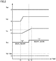
- FIG. 2 is an operation waveform diagram at the time of start-up of drive circuit 100a shown in FIG. 1 .
- FIG. 2 illustrates a waveform diagram when DC power (DC voltage Vd) is supplied from an external power supply to gate drive voltage generator 10a.
- gate drive voltage generator 10a In response to supply of DC voltage Vd from time ts, gate drive voltage generator 10a starts generation of gate drive voltage Vc. Gate drive voltage Vc is thus increased and gate drive voltage Vc is increased to a rated value at time tz.
- switch element 60 is maintained in the on state and switch element 50 is maintained in the off state.
- semiconductor switching element 200 can be maintained in the off state.
- false turn-on of semiconductor switching element 200 due to increase in gate voltage Vgt caused by unintended charging of a gate capacitance by a feedback capacitance of semiconductor switching element 200 with start-up of the main circuit at the time of start-up of the power supply can be prevented.
- gate resistor 30 generally has a resistance value approximately from several ohms ( ⁇ ) to several ten ohms ( ⁇ ) as described above, formation of such a current path may lead to occurrence of power loss equal to or higher than several ten watts (W) at gate resistor 30. There is concern that defective start-up of gate drive voltage generator 10a may occur due to this power loss.
- switch element 50 in the off state cuts off the current path including gate resistor 30 to short-circuited gate 203. Consequently, occurrence of power loss at gate resistor 30 and occurrence of defective start-up of gate drive voltage generator 10a can be prevented.
- switch element 50 is turned on and switch element 60 is turned off. Consequently, in semiconductor switching element 200, gate 203 is disconnected from source 202 and electrically connected to the output node of gate signal amplifier 20.
- gate voltage Vgt becomes controllable in accordance with the output from gate signal amplifier 20, and a state that semiconductor switching element 200 can be turned on and off in accordance with gate control signal Sgc, that is, a normal operating state of drive circuit 100a, is formed.
- a dead time as shown in FIG. 3 may also be introduced in operations by switch elements 50 and 60 at the time of output of electrical signal Sct (time tx).
- the dead time as shown in FIG. 3 can be provided by transmitting electrical signal Sct output from start-up sensor 70 to switch element 60 via a delay circuit (not shown) that provides a delay time corresponding to dead time Td and transmitting electrical signal Sct to switch element 50 not via the delay circuit.
- switch element 50 when switch element 50 is turned on after switch element 60 is turned off, both of switch elements 50 and 60 are turned off. Then, gate 203 of semiconductor switching element 200 is opened, and false turn-on of semiconductor switching element 200 may occur due to unintended charging of the gate capacitance described above.
- the drive circuit in the present first embodiment by complementarily turning on and off switch elements 50 and 60, a current path to the control electrode (gate 203) short-circuited for prevention of false turn-on can be cut off until start-up of the control power supply is sensed. Consequently, power loss at the gate resistor at the time of start-up of the power supply and occurrence of defective start-up of the gate drive voltage generator as well as occurrence of false turn-on of the semiconductor switching element can be prevented.
- a highly reliable drive circuit can thus be configured.
- Start-up sensor 70 can sense start-up of gate drive voltage generator 10a with a simplified configuration in accordance with comparison between gate drive voltage Vc and the criterion voltage.
- gate drive voltage generator 10a corresponds to one embodiment of the "drive voltage generator” and gate drive voltage Vc corresponds to the "drive voltage.”
- Gate signal amplifier 20 corresponds to the “signal amplifier”
- gate resistor 30 corresponds to the "resistive element”
- switch element 50 corresponds to the "first switch element”
- switch element 60 corresponds to the "second switch element.”
- FIG. 4 is a block diagram illustrating a configuration of a drive circuit according to a second embodiment.
- a drive circuit 100b according to the second embodiment is different from drive circuit 100a according to the first embodiment in including a gate drive voltage generator 10b instead of gate drive voltage generator 10a ( FIG. 1 ).
- Gate drive voltage generator 10b further generates a gate drive voltage Vn for negative biasing for turning off semiconductor switching element 200, in addition to gate drive voltage Vc for positive biasing for turning on semiconductor switching element 200.
- gate drive voltage generator 10b can be configured with two DC/DC converters for positive voltage generation and negative voltage generation.
- Gate drive voltage generator 10b outputs gate drive voltage Vc to power supply line PL whereas it outputs gate drive voltage Vn to power supply line NL.
- gate drive voltage generator 10b is further connected to a reference potential line that supplies a reference voltage (for example, GND), separately from power supply lines PL and NL.
- Gate drive voltage Vc is higher than the reference voltage (GND) and gate drive voltage Vn is lower than the reference voltage (GND) (that is, a negative voltage).
- Source output terminal 40b is connected to the reference potential line (for example, GL) and source 202 of semiconductor switching element 200.
- Start-up sensor 70 senses start-up of gate drive voltage generator 10b by receiving as input, a voltage of power supply line NL, that is, gate drive voltage Vn (negative voltage). When start-up sensor 70 senses start-up of gate drive voltage generator 10b, it outputs electrical signal Sct as in the first embodiment. Since drive circuit 100b according to the second embodiment is otherwise similar in configuration to drive circuit 100a according to the first embodiment, detailed description will not be repeated.
- FIG. 5 is an operation waveform diagram at the time of start-up of drive circuit 100b shown in FIG. 4 .
- FIG. 5 also illustrates a waveform diagram when DC power (DC voltage Vd) is supplied from an external power supply to gate drive voltage generator 10b.
- gate drive voltage generator 10b In response to supply of DC voltage Vd from time ts, gate drive voltage generator 10b starts generation of gate drive voltages Vc (positive voltage) and Vn (negative voltage). Gate drive voltage Vc thus increases and gate drive voltage Vn lowers. At time tz, gate drive voltage Vc increases to a rated value and gate drive voltage Vn lowers to a rated value.
- start-up sensor 70 senses start-up of gate drive voltage generator 10b.
- start-up sensor 70 senses start-up of gate drive voltage generator 10a or 10b.
- the dead time as in FIG. 3 can also be introduced into the operations by switch elements 50 and 60 at time ty.
- start-up of gate drive voltage generator 10b for switching drive circuit 100b to a normal operation state is determined based on gate drive voltage Vn on the negative bias side for turning off semiconductor switching element 200. Consequently, even when a rate of rise at the time of start-up of the power supply is different between the positive bias side and the negative bias side, false turn-on of semiconductor switching element 200 can reliably be prevented.
- gate drive voltage generator 10b corresponds to one embodiment of the "drive voltage generator”
- gate drive voltage Vc on the positive bias side corresponds to the "first drive voltage”
- gate drive voltage Vc on the negative bias side corresponds to the "second drive voltage.”
- a power conversion device to which the drive circuits described in the first and second embodiments are applied will be described in a third embodiment.
- FIG. 6 is a block diagram illustrating an exemplary configuration of a power conversion device according to the third embodiment.
- a power conversion device 300 controls power flow between an AC system and a DC system by interconnecting the AC system and the DC system to each other.
- Power conversion device 300 includes a three-phase transformer 305, a plurality of converter cells 310, and a reactor 320.
- the plurality of converter cells 310 are connected to form six phase arms between DC power lines 301 and 302 of the DC system.
- a primary side of three-phase transformer 305 is connected to a not-shown AC system.
- a secondary side of three-phase transformer 305 is connected to nodes Nu, Nv, and Nw.
- a plurality of converter cells 310 and reactor 320 that form a U-phase upper arm are connected in series between node Nu and DC power line 301.
- a plurality of converter cells 310 and reactor 320 that form a U-phase lower arm are connected in series between node Nu and DC power line 302.
- a plurality of converter cells 310 and reactors 320 are connected in series between node Nv and DC power lines 301 and 302 so as to form a V-phase upper arm and a V-phase lower arm.
- a plurality of converter cells 310 and reactors 320 are connected in series between node Nw and DC power lines 301 and 302 so as to form a W-phase upper arm and a W-phase lower arm.
- Power conversion device 300 thus configured with the plurality of converter cells 310 connected in series is generally called a modular multilevel converter (MMC) and it is applied to applications requiring output of a high voltage.
- MMC modular multilevel converter
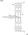
- FIG. 7 is a block diagram illustrating an exemplary configuration of each converter cell 310 of power conversion device 300.
- converter cell 310 includes semiconductor switching elements 200p and 200n connected in series, diodes 205p and 205n, an energy accumulation element 210, drive circuits lOOp and 100n, and a control power supply 220.
- Diodes 205p and 205n are connected in anti-parallel to semiconductor switching elements 200p and 200n, respectively.
- An arm 311 is configured with semiconductor switching element 200p and diode 205p and an arm 312 is configured with semiconductor switching element 200n and diode 205n.
- a MOSFET is illustrated as semiconductor switching elements 200p and 200n in an exemplary configuration in FIG. 7 , a semiconductor switching element of another type such as an IGBT can also be applied.
- Energy accumulation element 210 Arms 311 and 312 connected in series are connected in parallel to energy accumulation element 210. Output terminals To1 and To2 of converter cell 310 are connected in parallel to arm 312.
- a capacitor is employed as energy accumulation element 210.
- energy accumulation element 210 can be configured with an electrolytic capacitor or a film capacitor.
- Control power supply 220 is connected in parallel to energy accumulation element 210 and supplies electric power to drive circuits lOOp and 100n and other control circuits.
- a scheme for directly supplying electric power for control from a main circuit of converter cell 310 as in control power supply 220 is called self-supply or main circuit power supply.
- a known technique such as a configuration including a current limit resistor as an input or a configuration including a voltage division capacitor as an input can arbitrarily be applied as a specific configuration of control power supply 220.
- Drive circuit lOOp controls turn-on and turn-off of semiconductor switching element 200p in accordance with a gate control signal Sgcp and drive circuit 100n controls turn-on and turn-off of semiconductor switching element 200n in accordance with a gate control signal Sgcn.
- Each of drive circuits lOOp and 100n can be configured with drive circuit 100a according to the first embodiment or drive circuit 100b according to the second embodiment.
- Gate drive voltage generators 10a and 10b in respective Figs. 1 and 4 generate gate drive voltage Vc (or Vc and Vn) with a DC voltage supplied from control power supply 220, with control power supply 220 being adopted as the external power supply.
- Each of gate control signals Sgcp and Sgcn corresponds to gate control signal Sgc input to gate signal amplifier 20 in Figs. 1 and 4 .
- the main circuit includes at least one semiconductor switching element 200 and energy accumulation element 210.
- turn-on and turn-off of the semiconductor switching element can be controlled by using the drive circuit according to the first or second embodiment. Therefore, false turn-on of the semiconductor switching element can reliably be prevented and the semiconductor switching element can operate in a stable manner without occurrence of power loss or defective start-up of the drive circuit at the time of start-up.
- FIG. 7 illustrates an exemplary configuration in which a chopper circuit is provided as a main circuit configuration including converter cells 310
- any configuration of converter cell 310 is applicable, for example, by adopting a full bridge circuit for the main circuit.
- the configuration of the power conversion device described in the third embodiment is merely by way of example, and the drive circuit according to the first or second embodiment can be applied to drive the gate of the semiconductor switching element that makes up the main circuit, without the configuration of the main circuit of the power conversion device being particularly restricted.
- the first to third embodiments can also be applied to a control electrode of a current-driven semiconductor switching element (for example, a base of a bipolar transistor).
- a current-driven semiconductor switching element for example, a base of a bipolar transistor.
- the effect described in the first to third embodiments can be obtained also in this case by short-circuiting a negative electrode and the control electrode of the semiconductor switching element (of the current driven type) by means of switch element 60 until a voltage for driving the control electrode (corresponding to the gate drive voltage) rises, cutting off a current path to the control electrode by means of switch element 50, and interchanging on and off of switch elements 50 and 60 after rise of the voltage.
Landscapes
- Engineering & Computer Science (AREA)
- Power Engineering (AREA)
- Power Conversion In General (AREA)
- Inverter Devices (AREA)
Abstract
Description
- The present invention relates to a drive circuit and a power conversion device, and more particularly to a drive circuit that drives a semiconductor switching element and a power conversion device including the drive circuit.
- In a power conversion device, in order to control turn-on and turn-off of a semiconductor switching element provided in a main circuit, a drive circuit that drives a control electrode of the semiconductor switching element (which is also called a "gate drive circuit") is employed. In the power conversion device, a control power supply that supplies electric power to the drive circuit and a circuit that constructs another control system is provided. For the control power supply, a scheme for supplying electric power from a main circuit of the power conversion device has generally been adopted.
- For example, in a self-supply gate circuit described in Japanese Patent Laying-Open No.
10-285909 - PTL 1: Japanese Patent Laying-Open No.
10-285909 - In the gate circuit in
PTL 1, however, during the period for which the control power supply has not yet been established, the switch short-circuits a gate and an emitter of the semiconductor switching element configured with an insulated gate bipolar transistor (IGBT). Therefore, an output of a drive amplifier that supplies a gate current is kept connected to the emitter terminal of the semiconductor switching element with a gate resistor being interposed. - At this time, when supply of electric power to the gate circuit starts to start start-up of a power supply system of the gate circuit and a gate voltage starts to rise, a current flows through the gate resistor in accordance with the voltage applied to an output node of the drive amplifier, which results in power loss. Though a gate resistance value is determined to adjust a condition for driving the semiconductor switching element, it may also be as small as approximately several ohms (Ω). In such a case, power loss caused at the gate resistor during the period for which the control power supply has not yet been established may be expected to attain to several ten watts (W) or more. There is concern that such large power loss at the gate resistor is a cause for defective start-up of the power supply system of the gate circuit.
- The present invention was made to solve such a problem, and an object of the present invention is to prevent occurrence of power loss and false turn-on of a semiconductor switching element at the time of start-up of a power supply in a drive circuit that drives a control electrode of the semiconductor switching element.
- According to one aspect of the present invention, a drive circuit that drives a control electrode of a semiconductor switching element includes a drive voltage generator, a signal amplifier, a resistive element, first and second switch elements, and a start-up sensor. The drive voltage generator generates a drive voltage to be used for driving the control electrode from a voltage supplied from a power supply outside the drive circuit. The signal amplifier amplifies a control signal for control of turn-on and turn-off of the semiconductor switching element and outputs the amplified control signal. The resistive element is connected between an output terminal connected to the control electrode and an output node of the signal amplifier. The first switch element is connected in series to the resistive element between the output node and the output terminal. The second switch element short-circuits the output terminal when it is turned on. The start-up sensor outputs an electrical signal when it senses start-up of the drive voltage generator. The first switch element is configured with a normally-off switch that is turned on while the electrical signal is output. The second switch element is configured with a normally-on switch that is turned off while the electrical signal is output.
- According to the present invention, in the drive circuit that drives the control electrode of the semiconductor switching element, a current path to the control electrode that is short-circuited for prevention of false turn-on can be cut off until start-up of the control power supply is sensed. Therefore, occurrence of power loss and false turn-on of the semiconductor switching element can be prevented.
-
- FIG. 1
- is a block diagram showing a configuration of a drive circuit according to a first embodiment.
- FIG. 2
- is an operation waveform diagram at the time of start-up of the drive circuit shown in
FIG. 1 . - FIG. 3
- is an operation waveform diagram for illustrating a dead time between switches shown in
FIG. 1 . - FIG. 4
- is a block diagram illustrating a configuration of a drive circuit according to a second embodiment.
- FIG. 5
- is an operation waveform diagram at the time of start-up of the drive circuit shown in
FIG. 4 . - FIG. 6
- is a block diagram illustrating an exemplary configuration of a power conversion device according to a third embodiment.
- FIG. 7
- is a block diagram illustrating an exemplary configuration of a converter cell shown in
FIG. 6 . - An embodiment of the present invention will be described below in detail with reference to the drawings. The same or corresponding elements in the drawings below have the same reference characters allotted and description thereof will not be repeated in principle.
-
FIG. 1 is a block diagram illustrating a configuration of a drive circuit according to a first embodiment. - Referring to
FIG. 1 , adrive circuit 100a turns on and off asemiconductor switching element 200 in accordance with a control signal Sgc generated by a not-shown control circuit. -
Semiconductor switching element 200 includes apositive electrode 201, anegative electrode 202, and acontrol electrode 203, and it is controlled to one of an on state in which a current path is formed betweenpositive electrode 201 andnegative electrode 202 and an off state in which the current path is cut off, in accordance with a voltage or a current ofcontrol electrode 203. - In the present embodiment, an example in which
semiconductor switching element 200 is configured with a metal oxide semiconductor field effect transistor (MOSFET) which is a voltage-driven element will be described. In the MOSFET,positive electrode 201 serves as a drain,negative electrode 202 serves as a source, andcontrol electrode 203 serves as a gate.Positive electrode 201,negative electrode 202, andcontrol electrode 203 are also referred to below asdrain 201,source 202, andgate 203, respectively. Whensemiconductor switching element 200 is configured with an insulated gate bipolar transistor (IGBT),positive electrode 201 serves as a collector,negative electrode 202 serves as an emitter, andcontrol electrode 203 serves as a gate. - Control signal Sgc is also referred to as a gate control signal Sgc.
Drive circuit 100a outputs a voltage and a current that drivegate 203 to turn on and offsemiconductor switching element 200 in accordance with gate control signal Sgc. As is known,semiconductor switching element 200 is turned on when a gate voltage Vgt which is a voltage ofgate 203 with respect tosource 202 is higher than a threshold voltage (Vth). When gate voltage Vgt is lower than the threshold voltage (Vth),semiconductor switching element 200 is turned off. -
Drive circuit 100a according to the first embodiment includes a gatedrive voltage generator 10a, agate signal amplifier 20, agate resistor 30, agate output terminal 40a, asource output terminal 40b,switch elements up sensor 70. - Gate
drive voltage generator 10a is connected to a low-voltage side power supply line NL and a high-voltage side power supply line PL, and generates a gate drive voltage Vc from electric power supplied from a power supplyoutside drive circuit 100a (which is referred to as an "external power supply" below). Gatedrive voltage generator 10a outputs gate drive voltage Vc to high-voltage side power supply line PL. In the first embodiment, low-voltage side power supply line NL corresponds to a reference potential line for supplying a reference voltage (GND here). The reference voltage corresponds to a voltage ofsource 202. - For example, when the external power supply supplies AC power, gate
drive voltage generator 10a can be configured with an AC/DC converter. A known technique such as a half-wave rectifier circuit or a full-wave rectifier circuit including a diode or a pulse width modulation (PWM) rectifier circuit including a semiconductor switching element can be applied to the AC/DC converter. - When the external power supply supplies DC power, gate
drive voltage generator 10a can be configured with a DC/DC converter. A known technique such as a shunt regulator, a series regulator, or a switching regulator including a semiconductor switching element can be applied to the DC/DC converter. -
Gate signal amplifier 20 amplifies gate control signal Sgc to a voltage and a current sufficient for drivinggate 203 and outputs the amplified gate control signal to an output node No.Gate signal amplifier 20 can be configured, for example, with a push-pull type amplifier circuit. Alternatively, when gate control signal Sgc received from the outside is an optical signal,gate signal amplifier 20 is configured to have a light reception element disposed in its input stage and to perform a function to photoelectrically convert the received optical signal (gate control signal Sgc). -
Gate output terminal 40a is connected togate 203 ofsemiconductor switching element 200.Source output terminal 40b is connected to the reference potential line (low-voltage side power supply line NL here) andsource 202 ofsemiconductor switching element 200.Gate resistor 30 and normally-off switch element 50 are connected in series to each other between output node No ofgate signal amplifier 20 andgate output terminal 40a. - A resistance value of
gate resistor 30 is determined in consideration of a switching characteristic ofsemiconductor switching element 200 to be driven bydrive circuit 100a. In general, a resistance value approximately from several ohms (Ω) to several ten ohms (Ω) is adopted. Though a configuration in whichsingle gate resistor 30 is arranged is illustrated for simplification of description in the present embodiment,gate resistor 30 may be configured such that a gate resistance value is switched between a value at the time of turn-on and a value at the time of turn-off. For example, the gate resistance value can be switched by combining two resistive elements different in resistance value and at least one switching element. -
Switch element 50 can be configured with a normally-off semiconductor switch or a mechanical switch.Switch element 50 is turned on while an electrical signal Sct is output from start-upsensor 70, whereas it is turned off while electrical signal Sct is not output. - Normally-on
switch element 60 is connected betweengate output terminal 40a andsource output terminal 40b.Switch element 60 can be configured with a normally-on semiconductor switch or a mechanical switch.Switch element 60 is turned off while electrical signal Sct is output from start-upsensor 70, whereas it is turned on while electrical signal Sct is not output. Whileswitch element 60 is on,gate 203 andsource 202 ofsemiconductor switching element 200 are equal in potential (GND) andgate 203 is short-circuited. Thus, during an on period ofswitch element 60, false turn-on can be prevented by reliably maintainingsemiconductor switching element 200 in the off state. - Start-
up sensor 70 receives as an input, a voltage of power supply line PL, that is, gate drive voltage Vc generated by gatedrive voltage generator 10a. Start-up sensor 70 is configured, for example, with a comparator, and it compares gate drive voltage Vc with a predetermined criterion voltage Vt. When gate drive voltage Vc exceeds criterion voltage Vt, start-upsensor 70 senses start-up of gatedrive voltage generator 10b (in other words, start-up of a control power supply) and outputs electrical signal Sct. While gate drive voltage Vc is lower than criterion voltage Vt, electrical signal Sct is not output. - An operation of
drive circuit 100a according to the first embodiment at the time of start-up of the power supply will now be described with reference toFIG. 2 . -
FIG. 2 is an operation waveform diagram at the time of start-up ofdrive circuit 100a shown inFIG. 1 .FIG. 2 illustrates a waveform diagram when DC power (DC voltage Vd) is supplied from an external power supply to gatedrive voltage generator 10a. - Referring to
FIG. 2 , when external supply of power is started at time ts, DC voltage Vd rises. Before time ts at which supply of power is started, gate drive voltage Vc has not been generated (Vc = 0) and electrical signal Sct has not been generated either (Sct = "0"). - In response to supply of DC voltage Vd from time ts, gate
drive voltage generator 10a starts generation of gate drive voltage Vc. Gate drive voltage Vc is thus increased and gate drive voltage Vc is increased to a rated value at time tz. - When gate drive voltage Vc exceeds criterion voltage Vt (Vt > 0) at time tx (Vc > Vt), start-up
sensor 70 senses start-up of gate drive voltage Vc and outputs electrical signal Sct (Sct = "1"). During a period from time ts to time tx, electrical signal Sct is not output (Sct = "0") either, similarly to a period before time ts. - Therefore, throughout a period before start of external supply of power (before time ts) and a period from start of supply of power until sensing of start-up of gate
drive voltage generator 10a (from time ts to time tx),switch element 60 is maintained in the on state and switchelement 50 is maintained in the off state. By thus short-circuiting gate 203 andsource 202 ofsemiconductor switching element 200,semiconductor switching element 200 can be maintained in the off state. In particular, false turn-on ofsemiconductor switching element 200 due to increase in gate voltage Vgt caused by unintended charging of a gate capacitance by a feedback capacitance ofsemiconductor switching element 200 with start-up of the main circuit at the time of start-up of the power supply can be prevented. - Furthermore, occurrence of power loss due to opening of the output of
gate signal amplifier 20 in response to turn-off ofswitch element 50 and a flow of a current throughgate resistor 30 with start-up of gatedrive voltage generator 10a can be prevented. As described inPTL 1, when gate drive voltage Vc is started up, a current path from the output node ofgate signal amplifier 20 viagate resistor 30 andswitch element 60 may be formed. Sincegate resistor 30 generally has a resistance value approximately from several ohms (Ω) to several ten ohms (Ω) as described above, formation of such a current path may lead to occurrence of power loss equal to or higher than several ten watts (W) atgate resistor 30. There is concern that defective start-up of gatedrive voltage generator 10a may occur due to this power loss. - In contrast, in the drive circuit according to the present first embodiment, during a period until start-up of the gate drive voltage generator is confirmed,
switch element 50 in the off state cuts off the current path includinggate resistor 30 to short-circuitedgate 203. Consequently, occurrence of power loss atgate resistor 30 and occurrence of defective start-up of gatedrive voltage generator 10a can be prevented. - Furthermore, after start-up of gate
drive voltage generator 10a (after time tx),switch element 50 is turned on andswitch element 60 is turned off. Consequently, insemiconductor switching element 200,gate 203 is disconnected fromsource 202 and electrically connected to the output node ofgate signal amplifier 20. - Thus, gate voltage Vgt becomes controllable in accordance with the output from
gate signal amplifier 20, and a state thatsemiconductor switching element 200 can be turned on and off in accordance with gate control signal Sgc, that is, a normal operating state ofdrive circuit 100a, is formed. During a period for which gate control signal Sgc = "0" is output, a voltage (GND) of power supply line NL is output fromgate signal amplifier 20. Thus, throughout a period before time tx and a period after time tx, gate voltage Vgt does not exceed threshold voltage Vth in response to gate control signal Sgc = "0" andsemiconductor switching element 200 is maintained in the off state without being falsely turned on. - A dead time as shown in
FIG. 3 may also be introduced in operations byswitch elements - Referring to
FIG. 3 , after a state that electrical signal Sct is not output (Sct = "0") andswitch element 60 is on andswitch element 50 is off, electrical signal Sct is output (Sct = "1") and on and off ofswitch elements switch element 50,switch element 60 makes transition from on to off. - For example, the dead time as shown in
FIG. 3 can be provided by transmitting electrical signal Sct output from start-upsensor 70 to switchelement 60 via a delay circuit (not shown) that provides a delay time corresponding to dead time Td and transmitting electrical signal Sct to switchelement 50 not via the delay circuit. - Contrary to
FIG. 3 , whenswitch element 50 is turned on afterswitch element 60 is turned off, both ofswitch elements gate 203 ofsemiconductor switching element 200 is opened, and false turn-on ofsemiconductor switching element 200 may occur due to unintended charging of the gate capacitance described above. - In contrast, as shown in
FIG. 3 , by providing a dead time such thatswitch element 60 is turned off after turn-on ofswitch element 50, false turn-on ofsemiconductor switching element 200 can reliably be prevented, regardless of output fromgate signal amplifier 20. - According to the drive circuit in the present first embodiment, by complementarily turning on and off
switch elements - Start-
up sensor 70 can sense start-up of gatedrive voltage generator 10a with a simplified configuration in accordance with comparison between gate drive voltage Vc and the criterion voltage. - Furthermore, by introducing the dead time described with reference to
FIG. 3 into operations byswitch elements gate 203 is open can be prevented from being produced. Therefore, false turn-on of the semiconductor switching element to be driven by the drive circuit can reliably be prevented. - In the first embodiment, gate
drive voltage generator 10a corresponds to one embodiment of the "drive voltage generator" and gate drive voltage Vc corresponds to the "drive voltage."Gate signal amplifier 20 corresponds to the "signal amplifier,"gate resistor 30 corresponds to the "resistive element,"switch element 50 corresponds to the "first switch element," andswitch element 60 corresponds to the "second switch element." -
FIG. 4 is a block diagram illustrating a configuration of a drive circuit according to a second embodiment. - Referring to
FIG. 4 , adrive circuit 100b according to the second embodiment is different fromdrive circuit 100a according to the first embodiment in including a gatedrive voltage generator 10b instead of gatedrive voltage generator 10a (FIG. 1 ). - Gate
drive voltage generator 10b further generates a gate drive voltage Vn for negative biasing for turning offsemiconductor switching element 200, in addition to gate drive voltage Vc for positive biasing for turning onsemiconductor switching element 200. For example, gatedrive voltage generator 10b can be configured with two DC/DC converters for positive voltage generation and negative voltage generation. Gatedrive voltage generator 10b outputs gate drive voltage Vc to power supply line PL whereas it outputs gate drive voltage Vn to power supply line NL. - In the second embodiment, gate
drive voltage generator 10b is further connected to a reference potential line that supplies a reference voltage (for example, GND), separately from power supply lines PL and NL. Gate drive voltage Vc is higher than the reference voltage (GND) and gate drive voltage Vn is lower than the reference voltage (GND) (that is, a negative voltage).Source output terminal 40b is connected to the reference potential line (for example, GL) andsource 202 ofsemiconductor switching element 200. - Start-
up sensor 70 senses start-up of gatedrive voltage generator 10b by receiving as input, a voltage of power supply line NL, that is, gate drive voltage Vn (negative voltage). When start-upsensor 70 senses start-up of gatedrive voltage generator 10b, it outputs electrical signal Sct as in the first embodiment. Sincedrive circuit 100b according to the second embodiment is otherwise similar in configuration to drivecircuit 100a according to the first embodiment, detailed description will not be repeated. -
FIG. 5 is an operation waveform diagram at the time of start-up ofdrive circuit 100b shown inFIG. 4 .FIG. 5 also illustrates a waveform diagram when DC power (DC voltage Vd) is supplied from an external power supply to gatedrive voltage generator 10b. - Referring to
FIG. 5 , when external supply of power is started at time ts, DC voltage Vd rises. Before time ts at which supply of power is started, gate drive voltages Vc and Vn have not been generated (Vc = 0 and Vn = 0) and electrical signal Sct has not been generated either (Sct = "0"). - In response to supply of DC voltage Vd from time ts, gate
drive voltage generator 10b starts generation of gate drive voltages Vc (positive voltage) and Vn (negative voltage). Gate drive voltage Vc thus increases and gate drive voltage Vn lowers. At time tz, gate drive voltage Vc increases to a rated value and gate drive voltage Vn lowers to a rated value. - When gate drive voltage Vn becomes lower than a criterion voltage Vt# (Vt# < 0) at time ty (Vn < Vt#), start-up
sensor 70 senses start-up of gatedrive voltage generator 10b. Throughout the first and second embodiments, when an absolute value of gate drive voltage Vc or Vn exceeds an absolute value of a criterion voltage (positive or negative) set in advance in accordance with a polarity of the gate drive voltage (positive/negative), start-upsensor 70 senses start-up of gatedrive voltage generator - When start-up
sensor 70 senses start-up of gatedrive voltage generator 10b, it outputs electrical signal Sct (Sct = "1"). During a period from time ts to time ty, electrical signal Sct is not output either (Sct = "0") similarly to a period before time ts. Therefore, at the time of start-up of the power supply, switchelements drive voltage generator 10b also in the second embodiment as in the first embodiment. - Consequently, before time ty, gate voltage Vgt is controlled to Vgt = 0 owing to short-circuiting between
gate 203 andsource 202 by normally-onswitch element 50. Since gate control signal Sgc = "0" is output,gate signal amplifier 20 outputs gate drive voltage Vn of power supply line NL. Therefore, after time ty, a condition of Vgt = Vn (negative voltage) is satisfied. - Thus, also in
drive circuit 100b according to the second embodiment, throughout a period before time ty and a period after time ty, gate voltage Vgt does not exceed threshold voltage Vth in response to gate control signal Sgc = "0" andsemiconductor switching element 200 is maintained in the off state without being falsely turned on. The dead time as inFIG. 3 can also be introduced into the operations byswitch elements - In particular, in
drive circuit 100b according to the second embodiment, start-up of gatedrive voltage generator 10b for switchingdrive circuit 100b to a normal operation state is determined based on gate drive voltage Vn on the negative bias side for turning offsemiconductor switching element 200. Consequently, even when a rate of rise at the time of start-up of the power supply is different between the positive bias side and the negative bias side, false turn-on ofsemiconductor switching element 200 can reliably be prevented. - In the second embodiment, gate
drive voltage generator 10b corresponds to one embodiment of the "drive voltage generator," gate drive voltage Vc on the positive bias side corresponds to the "first drive voltage," and gate drive voltage Vc on the negative bias side corresponds to the "second drive voltage." - A power conversion device to which the drive circuits described in the first and second embodiments are applied will be described in a third embodiment.
-
FIG. 6 is a block diagram illustrating an exemplary configuration of a power conversion device according to the third embodiment. - Referring to
FIG. 6 , apower conversion device 300 according to the third embodiment controls power flow between an AC system and a DC system by interconnecting the AC system and the DC system to each other. -
Power conversion device 300 includes a three-phase transformer 305, a plurality ofconverter cells 310, and areactor 320. The plurality ofconverter cells 310 are connected to form six phase arms betweenDC power lines - A primary side of three-
phase transformer 305 is connected to a not-shown AC system. A secondary side of three-phase transformer 305 is connected to nodes Nu, Nv, and Nw. A plurality ofconverter cells 310 andreactor 320 that form a U-phase upper arm are connected in series between node Nu andDC power line 301. A plurality ofconverter cells 310 andreactor 320 that form a U-phase lower arm are connected in series between node Nu andDC power line 302. - Similarly, a plurality of
converter cells 310 andreactors 320 are connected in series between node Nv andDC power lines converter cells 310 andreactors 320 are connected in series between node Nw andDC power lines -
Power conversion device 300 thus configured with the plurality ofconverter cells 310 connected in series is generally called a modular multilevel converter (MMC) and it is applied to applications requiring output of a high voltage. -
FIG. 7 is a block diagram illustrating an exemplary configuration of eachconverter cell 310 ofpower conversion device 300. - Referring to
FIG. 7 ,converter cell 310 includessemiconductor switching elements diodes energy accumulation element 210, drive circuits lOOp and 100n, and acontrol power supply 220.Diodes semiconductor switching elements - An
arm 311 is configured withsemiconductor switching element 200p anddiode 205p and anarm 312 is configured withsemiconductor switching element 200n anddiode 205n. Though a MOSFET is illustrated assemiconductor switching elements FIG. 7 , a semiconductor switching element of another type such as an IGBT can also be applied. -
Arms energy accumulation element 210. Output terminals To1 and To2 ofconverter cell 310 are connected in parallel toarm 312. In the example inFIG. 6 , a capacitor is employed asenergy accumulation element 210. For example,energy accumulation element 210 can be configured with an electrolytic capacitor or a film capacitor. -
Control power supply 220 is connected in parallel toenergy accumulation element 210 and supplies electric power to drive circuits lOOp and 100n and other control circuits. A scheme for directly supplying electric power for control from a main circuit ofconverter cell 310 as incontrol power supply 220 is called self-supply or main circuit power supply. A known technique such as a configuration including a current limit resistor as an input or a configuration including a voltage division capacitor as an input can arbitrarily be applied as a specific configuration ofcontrol power supply 220. - Drive circuit lOOp controls turn-on and turn-off of
semiconductor switching element 200p in accordance with a gate control signal Sgcp and drive circuit 100n controls turn-on and turn-off ofsemiconductor switching element 200n in accordance with a gate control signal Sgcn. Each of drive circuits lOOp and 100n can be configured withdrive circuit 100a according to the first embodiment or drivecircuit 100b according to the second embodiment. - Gate
drive voltage generators Figs. 1 and4 generate gate drive voltage Vc (or Vc and Vn) with a DC voltage supplied fromcontrol power supply 220, withcontrol power supply 220 being adopted as the external power supply. Each of gate control signals Sgcp and Sgcn corresponds to gate control signal Sgc input togate signal amplifier 20 inFigs. 1 and4 . - In the third embodiment, a part in
Figs. 6 and7 except for drive circuits lOOp and 100n makes up the main circuit for power conversion. In other words, the main circuit includes at least onesemiconductor switching element 200 andenergy accumulation element 210. - In the power conversion device according to the third embodiment, turn-on and turn-off of the semiconductor switching element can be controlled by using the drive circuit according to the first or second embodiment. Therefore, false turn-on of the semiconductor switching element can reliably be prevented and the semiconductor switching element can operate in a stable manner without occurrence of power loss or defective start-up of the drive circuit at the time of start-up.
- Though
FIG. 7 illustrates an exemplary configuration in which a chopper circuit is provided as a main circuit configuration includingconverter cells 310, any configuration ofconverter cell 310 is applicable, for example, by adopting a full bridge circuit for the main circuit. Furthermore, the configuration of the power conversion device described in the third embodiment is merely by way of example, and the drive circuit according to the first or second embodiment can be applied to drive the gate of the semiconductor switching element that makes up the main circuit, without the configuration of the main circuit of the power conversion device being particularly restricted. - Though a voltage-driven MOSFET or IGBT is described by way of example as the semiconductor switching element to be driven by the drive circuit in the first to third embodiments, the first to third embodiments can also be applied to a control electrode of a current-driven semiconductor switching element (for example, a base of a bipolar transistor). The effect described in the first to third embodiments can be obtained also in this case by short-circuiting a negative electrode and the control electrode of the semiconductor switching element (of the current driven type) by means of
switch element 60 until a voltage for driving the control electrode (corresponding to the gate drive voltage) rises, cutting off a current path to the control electrode by means ofswitch element 50, and interchanging on and off ofswitch elements - It should be understood that the embodiments disclosed herein are illustrative and non-restrictive in every respect. The scope of the present invention is defined by the terms of the claims rather than the description above and is intended to include any modifications within the scope and meaning equivalent to the terms of the claims.
-
- 10a, 10b g
- ate drive voltage generator (gate drive voltage generation circuit)
- 20
- gate signal amplifier (gate signal amplification circuit)
- 30
- gate resistor
- 40a
- gate output terminal
- 40b
- source output terminal
- 50, 60
- switch element
- 70
- start-up sensor (start-up sensing circuit)
- 100a, 100b, 100n, 100p
- drive circuit
- 200, 200n, 200p
- semiconductor switching element
- 201
- drain (positive electrode)
- 202
- source (negative electrode)
- 203
- gate (control electrode)
- 205n, 205p
- diode
- 210
- energy accumulation element
- 220
- control power supply
- 300
- power conversion device
- 301, 302
- DC power line
- 305
- three-phase transformer
- 310
- converter cell
- 311, 312
- arm
- 320
- reactor
- NL, PL
- power supply line
- No
- output node
- Nu, Nv, Nw
- node
- Sct
- electrical signal
- Sgc, Sgcn, Sgcp
- gate control signal
- Td
- dead time
- Vc, Vn
- gate drive voltage
- Vd DC
- voltage
- Vgt
- gate voltage
- Vt, Vt#
- criterion voltage (gate drive voltage)
- Vth
- threshold voltage (semiconductor switching element)
Claims (8)
- A drive circuit that drives a control electrode of a semiconductor switching element comprising:a drive voltage generator to generate a drive voltage to be used for driving the control electrode from a voltage supplied from a power supply outside the drive circuit;a signal amplifier to amplify a control signal for control of turn-on and turn-off of the semiconductor switching element and outputs the amplified control signal;a resistive element connected between an output terminal connected to the control electrode and an output node of the signal amplifier;a first switch element connected in series to the resistive element between the output node and the output terminal;a second switch element to short-circuit the output terminal when the second switch element is turned on; anda start-up sensor that outputs an electrical signal when the start-up sensor senses start-up of the drive voltage generator,the first switch element being configured with a normally-off switch that is turned on while the electrical signal is output,the second switch element being configured with a normally-on switch that is turned off while the electrical signal is output.
- The drive circuit according to claim 1, wherein
the start-up sensor outputs the electrical signal when an absolute value of the drive voltage is larger than an absolute value of a predetermined criterion voltage and does not output the electrical signal when the absolute value of the drive voltage is smaller than the absolute value of the criterion voltage. - The drive circuit according to claim 1, wherein
the drive voltage generator generates a first drive voltage for turning on the semiconductor switching element and a second drive voltage for turning off the semiconductor switching element, and
the start-up sensor outputs the electrical signal when an absolute value of the second drive voltage is larger than an absolute value of a predetermined criterion voltage and does not output the electrical signal when the absolute value of the second drive voltage is smaller than the absolute value of the criterion voltage. - The drive circuit according to any one of claims 1 to 3, wherein
a dead time is provided such that the second switch element makes transition from on to off after the first switch element makes transition from off to on when the electrical signal is output. - The drive circuit according to any one of claims 1 to 4, wherein
the first switch element is configured with a normally-off semiconductor switch. - The drive circuit according to any one of claims 1 to 4, wherein
the second switch element is configured with a normally-on semiconductor switch. - A power conversion device comprising:at least one semiconductor switching element that makes up a main circuit; andthe drive circuit according to any one of claims 1 to 6 that drives the control electrode of the semiconductor switching element.
- The power conversion device according to claim 7, wherein
the main circuit includes an energy accumulation element, and
the power conversion device further comprises a control power supply that supplies a voltage to the drive voltage generator of the drive circuit by using energy accumulated in the energy accumulation element.
Applications Claiming Priority (2)
| Application Number | Priority Date | Filing Date | Title |
|---|---|---|---|
| JP2018134164 | 2018-07-17 | ||
| PCT/JP2019/027950 WO2020017506A1 (en) | 2018-07-17 | 2019-07-16 | Drive circuit and electric power conversion apparatus |
Publications (3)
| Publication Number | Publication Date |
|---|---|
| EP3826156A1 true EP3826156A1 (en) | 2021-05-26 |
| EP3826156A4 EP3826156A4 (en) | 2021-08-25 |
| EP3826156B1 EP3826156B1 (en) | 2026-01-28 |
Family
ID=69164143
Family Applications (1)
| Application Number | Title | Priority Date | Filing Date |
|---|---|---|---|
| EP19837566.9A Active EP3826156B1 (en) | 2018-07-17 | 2019-07-16 | Drive circuit and electric power conversion apparatus |
Country Status (4)
| Country | Link |
|---|---|
| US (1) | US11569727B2 (en) |
| EP (1) | EP3826156B1 (en) |
| JP (1) | JP6639763B1 (en) |
| WO (1) | WO2020017506A1 (en) |
Cited By (1)
| Publication number | Priority date | Publication date | Assignee | Title |
|---|---|---|---|---|
| WO2024200527A1 (en) * | 2023-03-31 | 2024-10-03 | Hitachi Energy Ltd | A method for starting up a plurality of series connected cells of a converter |
Families Citing this family (6)
| Publication number | Priority date | Publication date | Assignee | Title |
|---|---|---|---|---|
| JP7294084B2 (en) * | 2019-11-25 | 2023-06-20 | 株式会社デンソー | Short circuit detection device |
| JP7296331B2 (en) * | 2020-03-18 | 2023-06-22 | 株式会社 日立パワーデバイス | GATE DRIVE DEVICE AND GATE DRIVE METHOD, POWER SEMICONDUCTOR MODULE, AND POWER CONVERTER |
| JP7349069B2 (en) * | 2020-09-16 | 2023-09-22 | 株式会社オートネットワーク技術研究所 | drive device |
| CN113794469B (en) * | 2021-09-03 | 2023-09-22 | 中国科学院电工研究所 | Frequency multiplication gate driving circuit and frequency multiplication control method thereof |
| EP4199338A1 (en) * | 2021-12-15 | 2023-06-21 | General Electric Technology GmbH | Improvements in or relating to chain-link modules for voltage source converters |
| JP2025140670A (en) * | 2024-03-14 | 2025-09-29 | 株式会社日立製作所 | Power converter and inverter device |
Family Cites Families (19)
| Publication number | Priority date | Publication date | Assignee | Title |
|---|---|---|---|---|
| JPH10285909A (en) * | 1997-04-11 | 1998-10-23 | Toshiba Fa Syst Eng Kk | Power supply self-contained gate circuit |
| JP4347249B2 (en) * | 2005-03-31 | 2009-10-21 | 富士通マイクロエレクトロニクス株式会社 | DC-DC converter, control circuit for DC-DC converter, and control method for DC-DC converter |
| JP2012100437A (en) * | 2010-11-02 | 2012-05-24 | Denso Corp | Electronic equipment |
| JP5282782B2 (en) * | 2010-12-14 | 2013-09-04 | 株式会社デンソー | Switching element drive circuit |
| JP2012199763A (en) * | 2011-03-22 | 2012-10-18 | Sanken Electric Co Ltd | Gate drive circuit |
| JP5344056B2 (en) * | 2011-03-28 | 2013-11-20 | 株式会社デンソー | Switching element drive circuit |
| JP5840975B2 (en) * | 2012-02-22 | 2016-01-06 | 三菱電機株式会社 | Gate drive circuit |
| JPWO2014128942A1 (en) * | 2013-02-25 | 2017-02-02 | 株式会社日立製作所 | Semiconductor device driving apparatus |
| US9106134B2 (en) * | 2013-06-21 | 2015-08-11 | O2Micro, Inc. | Power transfer devices |
| US9184655B2 (en) * | 2014-03-17 | 2015-11-10 | Semiconductor Components Industries, Llc | Method and semiconductor device for a dedicated startup sequence in a resonant converter |
| DE102014214260B4 (en) * | 2014-04-24 | 2023-03-30 | Fraunhofer-Gesellschaft zur Förderung der angewandten Forschung e.V. | Device for switching a semiconductor-based switch and sensor for detecting a rate of change of current at a semiconductor-based switch |
| CN106104993B (en) * | 2014-05-30 | 2019-05-10 | 三菱电机株式会社 | Driving circuits for power semiconductor elements |
| EP3219010B1 (en) * | 2014-11-11 | 2020-07-08 | Maschinenfabrik Reinhausen GmbH | Resistor emulation and gate boost |
| JP6045765B1 (en) * | 2015-05-20 | 2016-12-14 | 三菱電機株式会社 | Power conversion device and vehicle drive system using the same |
| US9929652B1 (en) * | 2015-12-08 | 2018-03-27 | Navitas Semiconductor, Inc. | GaN FET with integrated driver and slew rate control |
| US9998110B2 (en) * | 2016-11-04 | 2018-06-12 | Infineon Technologies Austria Ag | System and method for variable impedance gate driver |
| JP2018191370A (en) * | 2017-04-28 | 2018-11-29 | 株式会社デンソー | Power supply |
| JP6992498B2 (en) * | 2017-12-26 | 2022-01-13 | 株式会社デンソー | Drive circuit of the switch to be driven |
| US10622994B2 (en) * | 2018-06-07 | 2020-04-14 | Vishay-Siliconix, LLC | Devices and methods for driving a semiconductor switching device |
-
2019
- 2019-07-16 EP EP19837566.9A patent/EP3826156B1/en active Active
- 2019-07-16 JP JP2019562009A patent/JP6639763B1/en active Active
- 2019-07-16 WO PCT/JP2019/027950 patent/WO2020017506A1/en not_active Ceased
- 2019-07-16 US US17/054,786 patent/US11569727B2/en active Active
Cited By (1)
| Publication number | Priority date | Publication date | Assignee | Title |
|---|---|---|---|---|
| WO2024200527A1 (en) * | 2023-03-31 | 2024-10-03 | Hitachi Energy Ltd | A method for starting up a plurality of series connected cells of a converter |
Also Published As
| Publication number | Publication date |
|---|---|
| JPWO2020017506A1 (en) | 2020-07-27 |
| JP6639763B1 (en) | 2020-02-05 |
| EP3826156B1 (en) | 2026-01-28 |
| EP3826156A4 (en) | 2021-08-25 |
| WO2020017506A1 (en) | 2020-01-23 |
| US11569727B2 (en) | 2023-01-31 |
| US20210234454A1 (en) | 2021-07-29 |
Similar Documents
| Publication | Publication Date | Title |
|---|---|---|
| EP3826156B1 (en) | Drive circuit and electric power conversion apparatus | |
| US11502685B2 (en) | Gate drive circuit and control circuit for switching circuit, and switching power supply | |
| US20190386483A1 (en) | Igbt short-circuit detection and protection circuit and igbt-based controllable rectifier circuit | |
| US6271712B1 (en) | Synchronous rectifier and method of operation | |
| EP3813239B1 (en) | Self-feeding circuit and power conversion device | |
| US11368101B2 (en) | Power conversion system | |
| EP3654517A1 (en) | Operating a modular multilevel converter | |
| JP2016005289A (en) | Power conversion device having deterioration diagnosis function | |
| US20210218345A1 (en) | Power conversion device | |
| US10056837B2 (en) | DC-DC converter and power source device | |
| US20250317138A1 (en) | Power switching device operable to reduce on-resistance and extend short circuit withstand time | |
| US7248093B2 (en) | Bipolar bootstrap top switch gate drive for half-bridge semiconductor power topologies | |
| US11404953B2 (en) | Drive circuit for power semiconductor element and power semiconductor module employing the same | |
| US11652398B2 (en) | Voltage source converters | |
| US7075271B2 (en) | Power controlling apparatus with power converting circuit | |
| US10931273B1 (en) | Circuit for controlling a switching device to deliver power to a load | |
| US10630195B2 (en) | Converter and power conversion device using same | |
| US12494781B2 (en) | Semiconductor relay device | |
| US20180091035A1 (en) | Control circuit | |
| EP3242390B1 (en) | Power control apparatus for sub-module of mmc converter | |
| US12494708B2 (en) | Circuitry and method for transitioning between modes of operation during an electrical fault | |
| US12272941B2 (en) | Overcurrent protection circuit and power converter | |
| US11611291B2 (en) | Power system and pulse width modulation method therefor | |
| US20240223102A1 (en) | Power inverter and method for controlling a power inverter | |
| EP4633019A1 (en) | Push-pull transformer, dc-dc converter, and uninterruptible power supply |
Legal Events
| Date | Code | Title | Description |
|---|---|---|---|
| STAA | Information on the status of an ep patent application or granted ep patent |
Free format text: STATUS: THE INTERNATIONAL PUBLICATION HAS BEEN MADE |
|
| PUAI | Public reference made under article 153(3) epc to a published international application that has entered the european phase |
Free format text: ORIGINAL CODE: 0009012 |
|
| STAA | Information on the status of an ep patent application or granted ep patent |
Free format text: STATUS: REQUEST FOR EXAMINATION WAS MADE |
|
| 17P | Request for examination filed |
Effective date: 20201217 |
|
| AK | Designated contracting states |
Kind code of ref document: A1 Designated state(s): AL AT BE BG CH CY CZ DE DK EE ES FI FR GB GR HR HU IE IS IT LI LT LU LV MC MK MT NL NO PL PT RO RS SE SI SK SM TR |
|
| A4 | Supplementary search report drawn up and despatched |
Effective date: 20210727 |
|
| RIC1 | Information provided on ipc code assigned before grant |
Ipc: H02M 1/08 20060101AFI20210721BHEP Ipc: H02M 7/48 20070101ALI20210721BHEP Ipc: H03K 17/22 20060101ALI20210721BHEP Ipc: H03K 17/0812 20060101ALI20210721BHEP Ipc: H02M 1/36 20070101ALI20210721BHEP |
|
| DAV | Request for validation of the european patent (deleted) | ||
| DAX | Request for extension of the european patent (deleted) | ||
| STAA | Information on the status of an ep patent application or granted ep patent |
Free format text: STATUS: EXAMINATION IS IN PROGRESS |
|
| 17Q | First examination report despatched |
Effective date: 20230511 |
|
| GRAP | Despatch of communication of intention to grant a patent |
Free format text: ORIGINAL CODE: EPIDOSNIGR1 |
|
| STAA | Information on the status of an ep patent application or granted ep patent |
Free format text: STATUS: GRANT OF PATENT IS INTENDED |
|
| INTG | Intention to grant announced |
Effective date: 20250922 |
|
| GRAS | Grant fee paid |
Free format text: ORIGINAL CODE: EPIDOSNIGR3 |
|
| GRAA | (expected) grant |
Free format text: ORIGINAL CODE: 0009210 |
|
| STAA | Information on the status of an ep patent application or granted ep patent |
Free format text: STATUS: THE PATENT HAS BEEN GRANTED |
|
| AK | Designated contracting states |
Kind code of ref document: B1 Designated state(s): AL AT BE BG CH CY CZ DE DK EE ES FI FR GB GR HR HU IE IS IT LI LT LU LV MC MK MT NL NO PL PT RO RS SE SI SK SM TR |
|
| REG | Reference to a national code |
Ref country code: CH Ref legal event code: F10 Free format text: ST27 STATUS EVENT CODE: U-0-0-F10-F00 (AS PROVIDED BY THE NATIONAL OFFICE) Effective date: 20260128 Ref country code: GB Ref legal event code: FG4D |
|
| REG | Reference to a national code |
Ref country code: DE Ref legal event code: R096 Ref document number: 602019080853 Country of ref document: DE |
|
| REG | Reference to a national code |
Ref country code: IE Ref legal event code: FG4D |