EP3825827A1 - Touch display device and display panel - Google Patents
Touch display device and display panel Download PDFInfo
- Publication number
- EP3825827A1 EP3825827A1 EP20182111.3A EP20182111A EP3825827A1 EP 3825827 A1 EP3825827 A1 EP 3825827A1 EP 20182111 A EP20182111 A EP 20182111A EP 3825827 A1 EP3825827 A1 EP 3825827A1
- Authority
- EP
- European Patent Office
- Prior art keywords
- touch
- area
- touch electrode
- critical dimension
- electrode metal
- Prior art date
- Legal status (The legal status is an assumption and is not a legal conclusion. Google has not performed a legal analysis and makes no representation as to the accuracy of the status listed.)
- Granted
Links
Images







Classifications
-
- G—PHYSICS
- G06—COMPUTING OR CALCULATING; COUNTING
- G06F—ELECTRIC DIGITAL DATA PROCESSING
- G06F3/00—Input arrangements for transferring data to be processed into a form capable of being handled by the computer; Output arrangements for transferring data from processing unit to output unit, e.g. interface arrangements
- G06F3/01—Input arrangements or combined input and output arrangements for interaction between user and computer
- G06F3/03—Arrangements for converting the position or the displacement of a member into a coded form
- G06F3/041—Digitisers, e.g. for touch screens or touch pads, characterised by the transducing means
- G06F3/044—Digitisers, e.g. for touch screens or touch pads, characterised by the transducing means by capacitive means
- G06F3/0447—Position sensing using the local deformation of sensor cells
-
- G—PHYSICS
- G06—COMPUTING OR CALCULATING; COUNTING
- G06F—ELECTRIC DIGITAL DATA PROCESSING
- G06F3/00—Input arrangements for transferring data to be processed into a form capable of being handled by the computer; Output arrangements for transferring data from processing unit to output unit, e.g. interface arrangements
- G06F3/01—Input arrangements or combined input and output arrangements for interaction between user and computer
- G06F3/03—Arrangements for converting the position or the displacement of a member into a coded form
- G06F3/041—Digitisers, e.g. for touch screens or touch pads, characterised by the transducing means
- G06F3/0416—Control or interface arrangements specially adapted for digitisers
- G06F3/0418—Control or interface arrangements specially adapted for digitisers for error correction or compensation, e.g. based on parallax, calibration or alignment
- G06F3/04186—Touch location disambiguation
-
- G—PHYSICS
- G06—COMPUTING OR CALCULATING; COUNTING
- G06F—ELECTRIC DIGITAL DATA PROCESSING
- G06F3/00—Input arrangements for transferring data to be processed into a form capable of being handled by the computer; Output arrangements for transferring data from processing unit to output unit, e.g. interface arrangements
- G06F3/01—Input arrangements or combined input and output arrangements for interaction between user and computer
- G06F3/03—Arrangements for converting the position or the displacement of a member into a coded form
- G06F3/041—Digitisers, e.g. for touch screens or touch pads, characterised by the transducing means
- G06F3/0416—Control or interface arrangements specially adapted for digitisers
-
- G—PHYSICS
- G06—COMPUTING OR CALCULATING; COUNTING
- G06F—ELECTRIC DIGITAL DATA PROCESSING
- G06F3/00—Input arrangements for transferring data to be processed into a form capable of being handled by the computer; Output arrangements for transferring data from processing unit to output unit, e.g. interface arrangements
- G06F3/01—Input arrangements or combined input and output arrangements for interaction between user and computer
- G06F3/03—Arrangements for converting the position or the displacement of a member into a coded form
- G06F3/041—Digitisers, e.g. for touch screens or touch pads, characterised by the transducing means
- G06F3/0412—Digitisers structurally integrated in a display
-
- G—PHYSICS
- G06—COMPUTING OR CALCULATING; COUNTING
- G06F—ELECTRIC DIGITAL DATA PROCESSING
- G06F3/00—Input arrangements for transferring data to be processed into a form capable of being handled by the computer; Output arrangements for transferring data from processing unit to output unit, e.g. interface arrangements
- G06F3/01—Input arrangements or combined input and output arrangements for interaction between user and computer
- G06F3/03—Arrangements for converting the position or the displacement of a member into a coded form
- G06F3/041—Digitisers, e.g. for touch screens or touch pads, characterised by the transducing means
- G06F3/0414—Digitisers, e.g. for touch screens or touch pads, characterised by the transducing means using force sensing means to determine a position
- G06F3/04142—Digitisers, e.g. for touch screens or touch pads, characterised by the transducing means using force sensing means to determine a position the force sensing means being located peripherally, e.g. disposed at the corners or at the side of a touch sensing plate
-
- G—PHYSICS
- G06—COMPUTING OR CALCULATING; COUNTING
- G06F—ELECTRIC DIGITAL DATA PROCESSING
- G06F3/00—Input arrangements for transferring data to be processed into a form capable of being handled by the computer; Output arrangements for transferring data from processing unit to output unit, e.g. interface arrangements
- G06F3/01—Input arrangements or combined input and output arrangements for interaction between user and computer
- G06F3/03—Arrangements for converting the position or the displacement of a member into a coded form
- G06F3/041—Digitisers, e.g. for touch screens or touch pads, characterised by the transducing means
- G06F3/0414—Digitisers, e.g. for touch screens or touch pads, characterised by the transducing means using force sensing means to determine a position
- G06F3/04144—Digitisers, e.g. for touch screens or touch pads, characterised by the transducing means using force sensing means to determine a position using an array of force sensing means
-
- G—PHYSICS
- G06—COMPUTING OR CALCULATING; COUNTING
- G06F—ELECTRIC DIGITAL DATA PROCESSING
- G06F3/00—Input arrangements for transferring data to be processed into a form capable of being handled by the computer; Output arrangements for transferring data from processing unit to output unit, e.g. interface arrangements
- G06F3/01—Input arrangements or combined input and output arrangements for interaction between user and computer
- G06F3/03—Arrangements for converting the position or the displacement of a member into a coded form
- G06F3/041—Digitisers, e.g. for touch screens or touch pads, characterised by the transducing means
- G06F3/0416—Control or interface arrangements specially adapted for digitisers
- G06F3/04164—Connections between sensors and controllers, e.g. routing lines between electrodes and connection pads
-
- G—PHYSICS
- G06—COMPUTING OR CALCULATING; COUNTING
- G06F—ELECTRIC DIGITAL DATA PROCESSING
- G06F3/00—Input arrangements for transferring data to be processed into a form capable of being handled by the computer; Output arrangements for transferring data from processing unit to output unit, e.g. interface arrangements
- G06F3/01—Input arrangements or combined input and output arrangements for interaction between user and computer
- G06F3/03—Arrangements for converting the position or the displacement of a member into a coded form
- G06F3/041—Digitisers, e.g. for touch screens or touch pads, characterised by the transducing means
- G06F3/044—Digitisers, e.g. for touch screens or touch pads, characterised by the transducing means by capacitive means
- G06F3/0443—Digitisers, e.g. for touch screens or touch pads, characterised by the transducing means by capacitive means using a single layer of sensing electrodes
-
- G—PHYSICS
- G06—COMPUTING OR CALCULATING; COUNTING
- G06F—ELECTRIC DIGITAL DATA PROCESSING
- G06F3/00—Input arrangements for transferring data to be processed into a form capable of being handled by the computer; Output arrangements for transferring data from processing unit to output unit, e.g. interface arrangements
- G06F3/01—Input arrangements or combined input and output arrangements for interaction between user and computer
- G06F3/03—Arrangements for converting the position or the displacement of a member into a coded form
- G06F3/041—Digitisers, e.g. for touch screens or touch pads, characterised by the transducing means
- G06F3/044—Digitisers, e.g. for touch screens or touch pads, characterised by the transducing means by capacitive means
- G06F3/0446—Digitisers, e.g. for touch screens or touch pads, characterised by the transducing means by capacitive means using a grid-like structure of electrodes in at least two directions, e.g. using row and column electrodes
-
- G—PHYSICS
- G06—COMPUTING OR CALCULATING; COUNTING
- G06F—ELECTRIC DIGITAL DATA PROCESSING
- G06F3/00—Input arrangements for transferring data to be processed into a form capable of being handled by the computer; Output arrangements for transferring data from processing unit to output unit, e.g. interface arrangements
- G06F3/01—Input arrangements or combined input and output arrangements for interaction between user and computer
- G06F3/03—Arrangements for converting the position or the displacement of a member into a coded form
- G06F3/041—Digitisers, e.g. for touch screens or touch pads, characterised by the transducing means
- G06F3/044—Digitisers, e.g. for touch screens or touch pads, characterised by the transducing means by capacitive means
- G06F3/0448—Details of the electrode shape, e.g. for enhancing the detection of touches, for generating specific electric field shapes, for enhancing display quality
-
- G—PHYSICS
- G06—COMPUTING OR CALCULATING; COUNTING
- G06F—ELECTRIC DIGITAL DATA PROCESSING
- G06F3/00—Input arrangements for transferring data to be processed into a form capable of being handled by the computer; Output arrangements for transferring data from processing unit to output unit, e.g. interface arrangements
- G06F3/01—Input arrangements or combined input and output arrangements for interaction between user and computer
- G06F3/03—Arrangements for converting the position or the displacement of a member into a coded form
- G06F3/041—Digitisers, e.g. for touch screens or touch pads, characterised by the transducing means
- G06F3/047—Digitisers, e.g. for touch screens or touch pads, characterised by the transducing means using sets of wires, e.g. crossed wires
-
- G—PHYSICS
- G06—COMPUTING OR CALCULATING; COUNTING
- G06F—ELECTRIC DIGITAL DATA PROCESSING
- G06F2203/00—Indexing scheme relating to G06F3/00 - G06F3/048
- G06F2203/041—Indexing scheme relating to G06F3/041 - G06F3/045
- G06F2203/04103—Manufacturing, i.e. details related to manufacturing processes specially suited for touch sensitive devices
-
- G—PHYSICS
- G06—COMPUTING OR CALCULATING; COUNTING
- G06F—ELECTRIC DIGITAL DATA PROCESSING
- G06F2203/00—Indexing scheme relating to G06F3/00 - G06F3/048
- G06F2203/041—Indexing scheme relating to G06F3/041 - G06F3/045
- G06F2203/04111—Cross over in capacitive digitiser, i.e. details of structures for connecting electrodes of the sensing pattern where the connections cross each other, e.g. bridge structures comprising an insulating layer, or vias through substrate
-
- G—PHYSICS
- G06—COMPUTING OR CALCULATING; COUNTING
- G06F—ELECTRIC DIGITAL DATA PROCESSING
- G06F2203/00—Indexing scheme relating to G06F3/00 - G06F3/048
- G06F2203/041—Indexing scheme relating to G06F3/041 - G06F3/045
- G06F2203/04112—Electrode mesh in capacitive digitiser: electrode for touch sensing is formed of a mesh of very fine, normally metallic, interconnected lines that are almost invisible to see. This provides a quite large but transparent electrode surface, without need for ITO or similar transparent conductive material
-
- H—ELECTRICITY
- H10—SEMICONDUCTOR DEVICES; ELECTRIC SOLID-STATE DEVICES NOT OTHERWISE PROVIDED FOR
- H10K—ORGANIC ELECTRIC SOLID-STATE DEVICES
- H10K59/00—Integrated devices, or assemblies of multiple devices, comprising at least one organic light-emitting element covered by group H10K50/00
- H10K59/40—OLEDs integrated with touch screens
Definitions
- aspects of the present disclosure relate to a touch display device, and more particularly, to a touch display device and a display panel capable of improved touch sensitivity.
- LCD liquid crystal display
- PDP plasma display panel
- OLED organic light emitting diode
- a touch display device with a touch-based input structure that allows the user to easily, intuitively and conveniently input information or commands by escaping from a conventional input method such as a button, a keyboard, and a mouse.
- Such a touch display device should grasp the presence or absence of a user's touch and accurately detect touch coordinates in order to provide a touch-based input structure.
- capacitance-based touch sensing method is widely used for detecting presence or absence of touch and touch coordinates based on a change in capacitance formed on a plurality of touch electrodes on a display panel.
- the edge area of the display panel is recently used as a region capable of displaying and touching in view of design.
- the inventors have realized that since a step between a touch electrode metal and a lower electrode layer decreases due to the curvature of the display panel in the edge area of the touch display device, there is a problem that decreases the touch sensitivity due to an undesirable parasitic capacitance.
- the inventors proposed to provide a touch display device and a display panel capable of obtaining improved touch sensitivity by compensation for the critical dimension of touch electrode metals formed in the edge area of the display panel.
- the inventors of the present disclosure provide a touch display device and a display panel capable of effective touch sensing by variously modifying the compensation for the critical dimension of touch electrode metals formed in edge area of the display panel.
- a touch display device includes a display panel comprised of an inner area forming a first step between first touch electrode metals with first critical dimension and lower electrode layer and an edge area having at least one of CD compensation area, which is located outside of the inner area, forming a second step between second touch electrode metals with second critical dimension larger than the first critical dimension and the lower electrode layer, and a touch circuit for sensing touch presence or touch location by using a touch sensing signal received from the touch electrode metals.
- the first step is maintained at a constant value.
- the lower electrode layer is a cathode electrode of a light emitting element.
- the second critical dimension has a value larger than the first critical dimension by a constant gap.
- the second step has a smaller size than the first step and is maintained at a constant value.
- the touch display device further includes a step decline area in which the step between the touch electrode metal and the lower electrode layer decreases adjacent to the CD compensation area.
- a step decline ratio of the step decline area is the same or different when the step decline area is formed as a plurality of areas.
- the critical dimension of the touch electrode metal formed in the CD compensation area increases as the distance from the inner area increases when the CD compensation area is formed as a plurality of areas.
- the critical dimension of the touch electrode metal formed in the CD compensation area increases at a constant ratio as the distance from the inner area increases.
- a display panel includes an inner area forming a first step between first touch electrode metals with first critical dimension and lower electrode layer, and an edge area having at least one of CD compensation area, which is located outside of the inner area, forming a second step between second touch electrode metals with second critical dimension larger than the first critical dimension and the lower electrode layer.
- FIG. 1 is a diagram schematically illustrating a touch display device according to one or more aspects of the present disclosure.
- a touch display device 100 may provide an image display function for displaying an image and a touch sensing function for sensing a user's touch.
- the touch display device 100 may include a display panel 110 in which data lines and gate lines are disposed for displaying an image, and a display driving circuit for driving the display panel 110.
- the display driving circuit functionally may include a data driving circuit for driving the data lines, a gate driving circuit for driving the gate lines, and a timing controller for controlling the data driving circuit and the gate driving circuit.
- the display driving circuit may be implemented with one or more integrated circuits.
- the touch display device 100 may include a touch screen panel in which a plurality of touch electrode TE are disposed for touch sensing, and a touch circuit 130 for driving of the touch screen panel and sensing touch.
- the touch screen panel of the touch display device 100 may be an external type that is manufactured separately from the display panel 110 and bonded to the display panel 110, or may be an embedded type that is manufactured together with the display panel 110 and located inside the display panel 110. Hereinafter, it will be described on the assumption that the touch screen panel is embedded in the display panel 110.
- the touch circuit 130 supplies a touch driving signal to the display panel 110 to drive the display panel 110, receives a touch sensing signal from the display panel 110, and detects touch presence and touch coordinates based on it.
- the touch circuit 130 may be implemented by including a touch driving circuit that supplies touch driving signals and receives touch sensing signals, and a touch controller that detects touch presence and touch coordinates.
- the touch circuit 130 may be implemented as one or more components (e.g., an integrated circuit), or may be implemented separately from the display driving circuit.
- touch circuit 130 may be implemented by being integrated with a display driving circuit or an internal circuit thereof.
- touch driving circuit of the touch circuit 130 may be implemented as an integrated circuit together with the data driving circuit of the display driving circuit.
- the touch display device 100 may detect touch presence and touch coordinates based on capacitance formed on the touch electrode TE.
- the touch display device 100 may detect a touch in a mutual-capacitance method or in a self-capacitance method as capacitance-based touch sensing method.
- a plurality of touch electrode TE may be composed of driving electrodes receiving touch driving signals through touch driving line Tx, and sensing electrodes transmitting touch sensing signals through touch sensing line Rx by forming capacitance with the driving electrodes.
- the touch driving line Tx and the touch sensing line Rx may be referred to as a touch line.
- the touch sensing based on the mutual-capacitance method detects the touch presence and the touch coordinates based on the change of the mutual-capacitance generated between the driving electrodes and the sensing electrodes according to the pointer presence such as a finger or a pen (including a digital pen or a smart pen).
- each touch electrode TE serves as both a driving electrode and a sensing electrode. That is, a touch driving signal is applied to a touch electrode TE, and a touch sensing signal is transmitted from the touch electrode TE to which the touch driving signal is applied. Therefore, in the touch sensing based on the self-capacitance method, there is no distinction between the driving electrode and the sensing electrode.
- the touch display device 100 may detect a touch by the mutual-capacitance method, or may detect a touch by the self-capacitance method.
- the touch circuit 130 sequentially outputs touch driving signals to the plurality of touch electrode TE through the touch driving line Tx in the touch sensing period.
- the touch driving line Tx transmitting the touch driving signals may be disposed in a direction parallel to the data lines disposed on the display panel 110, and the touch sensing line Rx transmitting the touch sensing signals may be disposed in a direction parallel to the gate lines disposed on the display panel 110.
- the touch driving line Tx extends in the long axis direction of the display panel 110
- the touch sensing line Rx extends in the short axis direction of the display panel 110.
- the arrangement of the touch driving line Tx and the touch sensing line Rx may be changed according to the shape or structure of the touch display device 100.
- a touch driving signal may be applied and touch sensing may be performed while a scan signal is applied to the gate line disposed on the display panel 110.
- FIG. 2 is a diagram illustrating areas in which touch electrodes are disposed in a display panel according to one or more aspects of the present disclosure.
- an area in which the touch electrode TE is disposed in the display panel 110 may be divided into a first area 112 and a second area 114.
- the first area 112 may also be referred to as an inner area 112 as it is in a central region and the second area 114 is in a peripheral region.
- the second area 114 may be located adjacent to the first area 112 and may have sub-areas within the second area 114.
- the second area 114 may be referred to as an edge area 114 as it is adjacently located at both sides of the first area 112.
- the inner area 112 is a region of the central portion surrounded by the left and right edge areas 114, and may be a region formed in a flat planar structure. Also, a plurality of touch electrode TE with a constant step (e.g., a dimension such as height) from the lower electrode layer of the display panel 110 may be formed in the inner area 112.
- a constant step e.g., a dimension such as height
- the capacitance value according to the location in the inner area 112 may be constant.
- the edge area 114 is a region extending to a vertical direction in the left or right side of the inner area 112, and may be formed in a flat planar structure according to a structure of the display panel 110. However, the edge area 114 is recently formed as a round structure with some curvature in a latest touch display device 100 with a touch function made of a streamlined structure.
- the edge area 114 may be located on the left or right side of the inner area 112, but may be located on the upper or lower side of the inner area 112 according to the type of the display panel 110.
- the capacitance value due to touch sensing is decreased so that the touch sensitivity is reduced compared to the inner area 112.
- corner area of the upper or lower edge area 114 may also be formed in a round shape, and may be included in the edge area 114.
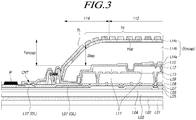
- FIG. 3 is a diagram illustrating a cross-section of a display panel in a touch display device.
- a polyimide (PI) layer L02 is located on a substrate or back plate L01.
- a buffer layer L03 may be located on the polyimide layer L02, and an interlayer insulating film L04 may be located on the buffer layer L03.
- a gate layer L05 may be present on the interlayer insulating film L04, and gate electrodes or the like may be provided on necessary positions of the gate layer L05.
- a gate insulating film L06 may be present on the gate layer L05.
- a source/drain layer L07 may be present on the gate insulating film L06.
- Signal lines such as data line DL and gate line GL, and source/drain electrodes of a plurality of transistors may be provided on the source/drain layer L07.
- a passivation layer L08 may be present on the source/drain layer L07.
- a planarization layer L09 may be located on the passivation layer L08, and a first electrode layer L10 may be present on the planarization layer L09, in the emission positions corresponding to the subpixels.
- a bank layer L11 is located on the first electrode layer L10, and an organic light-emitting layer L12 is located on the bank layer L11.
- a second electrode layer L13 commonly provided in all subpixel areas may be present on the organic light-emitting layer L12.
- An encapsulation layer L14 may be present on the second electrode layer L13 to prevent infiltration of moisture, air, or the like.
- a dam DAM may be present on a peripheral portion of the display panel 110.
- the encapsulation layer L14 may be a single layer or a two or more multi layers.
- the encapsulation layer L14 may be a composite layer comprised of one or more organic material layers and one or more inorganic material layers.
- the encapsulation layer L14 is illustrated as being a multilayer comprised of a first encapsulation layer L14a, a second encapsulation layer L14b, and a third encapsulation layer L14c.
- Each of the first encapsulation layer L14a, the second encapsulation layer L14b, and the third encapsulation layer L14c may be comprised of an organic material layer and an inorganic material layer.
- the touch electrode TE and the touch line TL are provided on the encapsulation layer L14.
- the touch electrode TE may be formed in a plate structure without an opening region, or may be formed in a mesh structure.
- the touch electrode TE of a mesh structure is formed as a touch electrode metal TEM patterned in a mesh shape, so that a plurality of opening regions may be formed.
- the touch electrode TE have other shapes and arrangements.
- the touch line TL electrically connected to the corresponding touch electrode TE on the encapsulation layer L14 extends to region without the touch electrode TE so as not to overlap with the touch electrode TE.
- the touch line TL bypasses a region in which the dam DAM is located, and extends to a region outside of the dam DAM, e.g., a portion adjacent to an integrated pad IP.
- the touch line TL may be connected to the data line DL on the source/drain layer L07 via contact hole CNT.
- the data line DL is electrically connected to the integrated pad IP in the region outside of the dam DAM
- the touch line TL and the touch electrode TE may be located on the same layer or different layers while being located on the encapsulation layer L14.
- the encapsulation layer L14 may have a selected thickness or a predetermined thickness Tencap in the inner area 112 and may have an influence on a time delay and touch sensitivity during the touch driving process and the touch sensing process.
- the thickness Tencap of the encapsulation layer L14 must be designed in consideration of the time delay and the touch sensitivity due to the touch driving.
- the display panel 110 may have a touch-on-encapsulation (TOE) structure in which touch electrode metal TEM and the touch line TL are located on the encapsulation layer L14.
- TOE touch-on-encapsulation
- the step between the touch electrode TE formed on the encapsulation layer L14 and the second electrode layer L13 corresponding to the cathode of a light-emitting element decrease in the direction toward a rounded edge area 114.
- Such a decrease in the step between the touch electrode TE and the lower second electrode layer L13 may cause capacitance values in the edge area 114 to be lower than those in the planar inner area 112, so that touch sensitivity may be decreased.
- FIG. 4 is a cross-sectional view schematically illustrating a step between touch electrode metals and a lower electrode layer in an inner area and an edge area of a touch display device
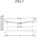
- FIG. 5 is a diagram illustrating a change in capacitance due to the steps between touch electrode metals and a lower electrode layer in an inner area and an edge area of a touch display device.
- the inner area 112 is formed in a flat structure, so that the step between the lower electrode layer corresponding to the cathode electrode and the touch electrode metal TEM is almost constant.
- the step between the lower electrode layer and the touch electrode metal TEM in the edge area 114 rapidly decreases as moving away from the inner area 112.
- the parasitic capacitance Cp formed between the lower electrode layer and the touch electrode metal TEM is rapidly increased by the step Step between the lower electrode layer and the touch electrode metal TEM.
- the parasitic capacitance Cp formed between the lower electrode layer and the touch electrode metal TEM increases as the step Step between the lower electrode layer and the touch electrode metal TEM decreases. If the increased parasitic capacitance Cp in edge area 114 is out of the allowable maximum range Max Spec for touch sensing, an operation of touch sensing may not be properly performed in the edge area 114.
- the inventors of the present disclosure provide a critical dimension (CD) compensation area capable of compensating for a change in capacitance due to a decrease in a step between the touch electrode metal TEM and the lower electrode layer in the edge area 114 of the touch display device 100, so that it is possible to obtain improved touch sensitivity.
- CD critical dimension
- FIG. 6 is a diagram schematically illustrating a display panel according to aspects of the present disclosure.
- an area in which a touch electrode metal TEM is disposed in the display panel 110 may be divided into an inner area 112 and an edge area 114.
- the inner area 112 is an area of the central portion surrounded by the left and right edge area 114, and is an area formed by a flat planar structure.
- a critical dimension (CD) of the touch electrode metal TEM formed in the inner area 112 corresponding to the line width of the touch electrode metal TEM may be formed to have a constant reference critical dimension Ref.
- the edge area 114 is an area formed in a round shape extending in the left or right, upper or lower direction of the inner area 112, and is an area where the step Step of the encapsulation layer Encap formed between the touch electrode metal TEM and the lower electrode layer is decreased in an outer direction away from the inner area 112.
- some region in the edge area 114 is formed as a CD compensation area Area2 and a critical dimension CD2 of the touch electrode metal TEM located in the CD compensation area Area2 is formed larger than a critical dimension CD1 of the touch electrode metal TEM located in the inner area 112.
- the edge area 114 may be divided into a step decline area Area1 and a CD compensation area Area2.
- the step decline area Area1 is an area formed at a position adjacent to the inner area 112 among the edge area 114, and is an area where the step Step between the touch electrode metal TEM and the lower electrode layer is decreased by the round shape of the edge area 114.
- the CD compensation area Area2 is an area having a constant width from the point where the step decline area Area1 ends, and the critical dimension CD2 of the touch electrode metal TEM formed in the CD compensation area Area2 is formed to be larger than the critical dimension CD1 of the touch electrode metal TEM formed in the inner area 112 by a constant gap Gap.
- the CD compensation area Area2 may be an area where the step Step2 between the touch electrode metal TEM and the lower electrode layer has a constant value.
- the critical dimension CD2 of the touch electrode metal TEM formed in the CD compensation area Area2 is larger than the critical dimension CD1 of the touch electrode metal TEM formed in the inner area 112, it is possible to diminish an increase of parasitic capacitance Cp formed between the touch electrode metal TEM and the lower electrode layer in the edge area 114.
- the critical dimension CD of the touch electrode metal TEM formed in the step decline area Area1 may be same value as the critical dimension CD1 of the touch electrode metal TEM formed in the inner area 112. In this case, it can be considered that the step decline area Area1 is included in the inner area 112.
- the critical dimension CD of the touch electrode metal TEM formed in the step decline area Area1 may be same value as the critical dimension CD2 of the touch electrode metal TEM formed in the CD compensation area Area2.
- the critical dimension CD of the touch electrode metal TEM formed in the step decline area Area1 is the same value as the critical dimension CD2 of the touch electrode metal TEM formed in the CD compensation area Area2, it can be considered that the step decline area Area1 is included in the CD compensation area Area2.
- Such CD compensation area Area2 may be formed in the edge area 114 located on the left or right side of the display panel 110, or formed in the upper or lower edge area 114 depending on the type of the display panel 110.
- FIG. 7 is a cross-sectional view schematically illustrating critical dimensions of touch electrode metals according to steps between touch electrode metals and a lower electrode layer in an inner area and an edge area of a display panel according to one or more aspects of the present disclosure.
- the inner area 112 in the display panel 110 may have a constant step Step1 which is a thickness of an encapsulation layer Encap formed between the touch electrode metal TEM and the lower electrode layer.
- an area adjacent to the inner area 112 in the edge area 114 corresponds to the step decline area Area1 where the step between the touch electrode metal TEM and a lower electrode layer decreases at a constant ratio.
- the width of the step decline area Area1 may vary depending on the size or structure of the display panel 110.
- the critical dimension CD2 of the touch electrode metal TEM in the CD compensation area Area2 is formed to be larger than the critical dimension CD1 of the touch electrode metal TEM formed in the inner area 112 in order to prevent an increase of parasitic capacitance Cp caused by a decrease of the step Step2 between the touch electrode metal TEM and the lower electrode layer.
- the step Step2 between the touch electrode metal TEM and the lower electrode layer may be a smaller value than the step Step1 of the inner area 112.
- the step Step2 in the CD compensation area Area2 may vary according to the width of the step decline area Area1 and the step decline ratio in the step decline area Area1.
- the CD compensation area Area2 may be formed as one area or may be formed as a plurality of areas in the edge area 114.
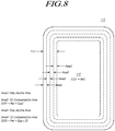
- FIG. 8 is a diagram illustrating a case, in which CD compensation area is formed as a plurality of areas in a display panel according to one or more aspects of the present disclosure
- FIG. 9 is a cross-sectional view schematically illustrating steps between touch electrode metals and a lower electrode layer when CD compensation area is formed as a plurality of areas in a display panel according to one or more aspects of the present disclosure.
- areas in which the touch electrode metal TEM is disposed in the display panel 110 may be divided into an inner area 112 and an edge area 114.
- the inner area 112 is an area of the central portion surrounded by the left and right edge area 114, and is formed by a flat planar structure.
- a critical dimension CD1 of the touch electrode metal TEM formed in the inner area 112 may have a constant reference critical dimension Ref.
- the edge area 114 is an area extending in the left or right, upper or lower direction of the inner area 112 and is formed in a round shape.
- the step Step between the touch electrode metal TEM and the lower electrode layer decreases toward the outer direction away from the inner area 112.
- the edge area 114 may be divided into a plurality of step decline areas Area1, Area3 and a plurality of CD compensation areas Area2, Area4.
- the step decline area Area1 is an area in which the step between the touch electrode metal TEM and the lower electrode layer is uniformly reduced by the round shape of the edge area 114 within the edge area 114.
- the CD compensation areas Area2, Area4 are areas having a constant width from the end point of the step decline areas Area1, Area3.
- the steps Step2, Step3 between the touch electrode metal TEM and the lower electrode layer are respectively maintained at each constant value, but the critical dimensions CD2, CD3 of the touch electrode metal TEM increases step by step as the distance from the inner area 112 increases.
- the CD compensation areas Area2, Area4 may be alternately formed adjacent to the step decline areas Area1, Area3 respectively.
- the first CD compensation area Area2 is formed in a position adjacent to the first step decline area Area1, and its step Step2 between the touch electrode metal TEM and the lower electrode layer is smaller than the step Step 2 between the touch electrode metal TEM and the lower electrode layer in the inner area 112.
- a second step decline area Area3 is formed from the end point of the first CD compensation area Area2 in which the critical dimension CD2 of the touch electrode metal TEM is constant.
- the step between the touch electrode metal TEM and the lower electrode layer decreases again.
- the step decline ratio of the second step decline area Area3 may be the same as or different from the step decline ratio of the first step decline area Area1.
- the second CD compensation area Area4 may be formed with a constant width from the end point of the second step decline area Area3.
- the critical dimension CD3 of the touch electrode metal TEM may be formed with larger size than the critical dimension CD2 of the touch electrode metal TEM in the first CD compensation area Area2.
- a gap Gap between the critical dimension CD3 of the touch electrode metal TEM formed in the second CD compensation area Area4 and the critical dimension CD2 of the touch electrode metal TEM formed in the first CD compensation area Area2 may be the same as or different from a gap between the critical dimension CD2 of the touch electrode metal TEM formed in the first CD compensation area Area2 and the critical dimension CD1 of the touch electrode metal TEM formed in the inner area 112.
- the critical dimension CD of the touch electrode metal TEM formed in the CD compensation area Are2, Area4 may increase at a constant ratio or at a different ratio as the distance from the inner area 112.
- the increase in the parasitic capacitance Cp formed by the step Step1 between the touch electrode metal TEM and the lower electrode layer in the edge area 114 may be diminished step by step, so that it is possible to effectively prevent the decrease in touch sensitivity due to the parasitic capacitance Cp.
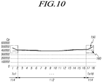
- FIG. 10 is a diagram illustrating a change in capacitance according to steps between touch electrode metals and a lower electrode layer in an inner area and an edge area of a touch display device according to one or more aspects of the present disclosure.
- forming a CD compensation area in the edge area 114 of the touch display device 100 according to one or more aspects of the present disclosure, it can be seen that the parasitic capacitance Cp formed between the touch electrode metal TEM and the lower electrode layer is reduced in the edge area 114.
- the CD compensation area may be applied to all the edge areas 114 including the corner area as well as the left or right, upper or lower side of the display panel 110.
- FIG. 11 is a diagram illustrating a change in capacitance according to steps between touch electrode metals and a lower electrode layer in eight edge areas of a touch display device according to one or more aspects of the present disclosure.
- the CD compensation area in the touch display device 100 may be formed in all edge areas 114 including the left or right, upper or lower side, and corner areas of the display panel 110.
- a touch display device that includes a display panel including an inner area and an edge area adjacent to the inner area.
- the edge area has at least one critical dimension (CD) compensation area.
- CD critical dimension
- the display panel includes a touch electrode metal.
- the touch electrode metal has a first touch electrode metal with a first critical dimension and a second touch electrode metal with a second critical dimension larger than the first critical dimension.
- the first touch electrode metal is indicative of a first part of the touch electrode metal and the second touch electrode metal is indicative of a second part of the touch electrode metal.
- the first part and the second part are adjacent to each other.
- the display panel includes a lower electrode layer.
- the display panel includes a first step between the first touch electrode metal and the lower electrode layer in the inner area.
- the display panel includes a second step between the second touch electrode metal and the lower electrode layer in the edge area.
- the display panel includes a touch circuit operatively connected to the display panel for sensing at least one of touch presence or touch location by using a touch sensing signal received from the first and second touch electrode metals.
- the first step is maintained at a constant value in at least some areas of the inner area.
- the lower electrode layer is a cathode electrode of a light emitting element.
- the second critical dimension has a value larger than the first critical dimension by a constant gap.
- the second step has a smaller size than the first step and the second step is maintained at a constant value in at least some areas of the edge area.
- the touch display device further includes a first step decline area between the first part and the second part of the touch electrode metal.
- the first step decline area has a height of a step between the touch electrode metal and the lower electrode layer decreasing from the first part to the second part.
- the step decline area is adjacent to a first CD compensation area of the at least one critical dimension (CD) compensation area.
- the touch electrode metal includes a third touch electrode metal indicative of a third part of the touch electrode metal.
- the third part is adjacent to the second part.
- the touch display device further includes a second step decline area between the second part and the third part of the touch electrode metal.
- the second step decline area has a height of a step between the touch electrode metal and the lower electrode layer decreasing from the second part to the third part.
- the second step decline area is adjacent to a second CD compensation area of the at least one critical dimension (CD) compensation area.
- a first step decline ratio of the first step decline area is substantially the same as a second step decline ratio of the second step decline area.
- a first step decline ratio of the first step decline area different from a second step decline ratio of the second step decline area.
- the critical dimension of the first and second touch electrode metals formed in the CD compensation area increases as the distance from the inner area increases when the CD compensation area is formed as a plurality of areas.
- the critical dimension of the first and second touch electrode metals formed in the CD compensation area increases at a constant ratio as the distance from the inner area increases.
- a display panel that includes an inner area having a first step between a first touch electrode metal with a first critical dimension and a lower electrode layer, and an edge area having at least one of CD compensation area, which is located outside of the inner area.
- the edge area has a second step between a second touch electrode metal with a second critical dimension larger than the first critical dimension and the lower electrode layer.
- the first step is maintained at a constant value.
- the lower electrode layer is a cathode electrode of a light emitting element.
- the second critical dimension has a value larger than the first critical dimension by a constant gap.
- the second step has a smaller size than the first step and is maintained at a constant value.
- the display panel further includes a step decline area in which the first step between the first touch electrode metal and the lower electrode layer decreases adjacent to the CD compensation area and in which the second step between the second touch electrode metal and the lower electrode layer decreases adjacent to the CD compensation area.
- a step decline ratio of the step decline area is the same or different when the step decline area is formed as a plurality of areas.
- the critical dimension of at least one of the first and second touch electrode metals formed in the CD compensation area increases as the distance from the inner area increases when the CD compensation area is formed as a plurality of areas.
- the critical dimension of at least one of the first and second touch electrode metals formed in the CD compensation area increases at a constant ratio as the distance from the inner area increases.
Landscapes
- Engineering & Computer Science (AREA)
- General Engineering & Computer Science (AREA)
- Theoretical Computer Science (AREA)
- Human Computer Interaction (AREA)
- Physics & Mathematics (AREA)
- General Physics & Mathematics (AREA)
- Quality & Reliability (AREA)
- Computer Networks & Wireless Communication (AREA)
- Position Input By Displaying (AREA)
- Electroluminescent Light Sources (AREA)
- Devices For Indicating Variable Information By Combining Individual Elements (AREA)
Abstract
Description
- This application claims priority from Korean Patent Application No.
10-2019-0149792, filed on November 20, 2019 - Aspects of the present disclosure relate to a touch display device, and more particularly, to a touch display device and a display panel capable of improved touch sensitivity.
- Along with the development of the information society, demands for display devices that display images are growing. In this regard, various types of display devices, such as liquid crystal display (LCD) devices, plasma display panel (PDP) display devices, and organic light emitting diode (OLED) display devices, have recently become popular.
- Among these display devices, there is a touch display device with a touch-based input structure that allows the user to easily, intuitively and conveniently input information or commands by escaping from a conventional input method such as a button, a keyboard, and a mouse.
- Such a touch display device should grasp the presence or absence of a user's touch and accurately detect touch coordinates in order to provide a touch-based input structure.
- To this end, among various touch sensing methods, capacitance-based touch sensing method is widely used for detecting presence or absence of touch and touch coordinates based on a change in capacitance formed on a plurality of touch electrodes on a display panel.
- Moreover, the edge area of the display panel is recently used as a region capable of displaying and touching in view of design.
- The inventors have realized that since a step between a touch electrode metal and a lower electrode layer decreases due to the curvature of the display panel in the edge area of the touch display device, there is a problem that decreases the touch sensitivity due to an undesirable parasitic capacitance.
- Based on the inventors work in fully locating and appreciating these issues, , the inventors proposed to provide a touch display device and a display panel capable of obtaining improved touch sensitivity by compensation for the critical dimension of touch electrode metals formed in the edge area of the display panel.
- In addition, the inventors of the present disclosure provide a touch display device and a display panel capable of effective touch sensing by variously modifying the compensation for the critical dimension of touch electrode metals formed in edge area of the display panel.
- The problems to be solved according to the aspects of the present disclosure, which will be described below, are not limited to the problems mentioned above, and other problems that are not mentioned will be clearly understood by those skilled in the art from the below description.
- A touch display device according to one or more aspects of the present disclosure includes a display panel comprised of an inner area forming a first step between first touch electrode metals with first critical dimension and lower electrode layer and an edge area having at least one of CD compensation area, which is located outside of the inner area, forming a second step between second touch electrode metals with second critical dimension larger than the first critical dimension and the lower electrode layer, and a touch circuit for sensing touch presence or touch location by using a touch sensing signal received from the touch electrode metals.
- In the touch display device according to one or more aspects of the present disclosure, the first step is maintained at a constant value.
- In the touch display device according to one or more aspects of the present disclosure, the lower electrode layer is a cathode electrode of a light emitting element.
- In the touch display device according to one or more aspects of the present disclosure, the second critical dimension has a value larger than the first critical dimension by a constant gap.
- In the touch display device according to one or more aspects of the present disclosure, the second step has a smaller size than the first step and is maintained at a constant value.
- The touch display device according to one or more aspects of the present disclosure further includes a step decline area in which the step between the touch electrode metal and the lower electrode layer decreases adjacent to the CD compensation area.
- In the touch display device according to one or more aspects of the present disclosure, a step decline ratio of the step decline area is the same or different when the step decline area is formed as a plurality of areas.
- In the touch display device according to one or more aspects of the present disclosure, the critical dimension of the touch electrode metal formed in the CD compensation area increases as the distance from the inner area increases when the CD compensation area is formed as a plurality of areas.
- In the touch display device according to one or more aspects of the present disclosure, the critical dimension of the touch electrode metal formed in the CD compensation area increases at a constant ratio as the distance from the inner area increases.
- A display panel according to one or more aspects of the present disclosure includes an inner area forming a first step between first touch electrode metals with first critical dimension and lower electrode layer, and an edge area having at least one of CD compensation area, which is located outside of the inner area, forming a second step between second touch electrode metals with second critical dimension larger than the first critical dimension and the lower electrode layer.
- According to aspects of the present disclosure, it is possible to obtain improved touch sensitivity by CD compensation for the edge area of the display panel.
- Further, according to aspects of the present disclosure, there is an effect capable of effectively sensing the touch by variously modifying the CD compensation for the edge area of the display panel.
- Advantages of the aspects of the present disclosure are not limited to the above advantages. The aspects of the present disclosure can achieve advantages which have not been mentioned above and will be apparently understood from the following description by those skilled in the art.
- The above and other objects, features, and advantages of the present disclosure will be more clearly understood from the following detailed description, taken in conjunction with the accompanying drawings, in which:
-
FIG. 1 is a diagram schematically illustrating a touch display device according to one or more aspects of the present disclosure; -
FIG. 2 is a diagram illustrating areas in which touch electrodes are disposed in a display panel according to one or more aspects of the present disclosure; -
FIG. 3 is a diagram illustrating a cross-section of a display panel in a touch display device; -
FIG. 4 is a cross-sectional view schematically illustrating a step between touch electrode metals and a lower electrode layer in an inner area and an edge area of a touch display device; -
FIG. 5 is a diagram illustrating a change in capacitance due to the steps between touch electrode metals and a lower electrode layer in an inner area and an edge area of a touch display device; -
FIG. 6 is a diagram schematically illustrating a display panel according to aspects of the present disclosure; -
FIG. 7 is a cross-sectional view schematically illustrating critical dimensions of touch electrode metals according to steps between touch electrode metals and a lower electrode layer in an inner area and an edge area of a display panel according to one or more aspects of the present disclosure; -
FIG. 8 is a diagram illustrating a case, in which CD compensation area is formed as a plurality of areas in a display panel according to one or more aspects of the present disclosure; -
FIG. 9 is a cross-sectional view schematically illustrating steps between touch electrode metals and a lower electrode layer when CD compensation area is formed as a plurality of areas in a display panel according to one or more aspects of the present disclosure; -
FIG. 10 is a diagram illustrating a change in capacitance according to steps between touch electrode metals and a lower electrode layer in an inner area and an edge area of a touch display device according to one or more aspects of the present disclosure; and -
FIG. 11 is a diagram illustrating a change in capacitance according to steps between touch electrode metals and a lower electrode layer in eight edge areas of a touch display device according to one or more aspects of the present disclosure. - Advantages and features of the present disclosure and methods for achieving the advantages or features will be apparent from aspects described below in detail with reference to the accompanying drawings. However, the disclosure is not limited to the aspects but can be modified in various forms. The aspects are provided merely for completing the disclosure of the disclosure and are provided for completely informing those skilled in the art of the scope of the disclosure. The scope of the disclosure is defined by only the appended claims.
- Shapes, sizes, ratios, angles, number of pieces, and the like illustrated in the drawings, which are provided for the purpose of explaining the aspects of the disclosure, are exemplary and thus the disclosure is not limited to the illustrated details. In the following description, like elements are referenced by like reference numerals. When it is determined that detailed description of the relevant known functions or configurations involved in the disclosure makes the gist of the disclosure obscure, the detailed description thereof will not be made. When "include," "have", "be constituted", and the like are mentioned in the specification, another element may be added unless "only" is used. A singular expression of an element includes two or more elements unless differently mentioned.
- In constructing elements in aspects of the disclosure, an error range is included even when explicit description is not made.
- For example, when positional relationships between two parts are described using 'on,' 'over,' 'under,' 'beside,' and the like, one or more other parts may be disposed between the two parts unless 'just' or 'direct' is used.
- In describing temporal relationships, for example, when the temporal order is described using 'after,' 'subsequent,' 'next,' and 'before,' a case which is not continuous may be included unless 'just' or 'direct' is used.
- In describing signal transmission relationships, for example, when 'a signal is transmitted from node A to node B,' a case in which the signal is transmitted from node A to node B via another node may be included unless 'just' or 'direct' is used.
- It will be understood that, although the terms "first," "second," and the like may be used herein to describe various elements, these elements should not be limited by these terms. These terms are only used to distinguish one element from another. For example, a first element could be termed a second element, and, similarly, a second element could be termed a first element, without departing from the scope of the present disclosure.
- Features of aspects of the disclosure can be coupled or combined with each other or separated from each other partially or on the whole and can be technically interlinked and driven in various forms. The aspects may be put into practice independently or in combination.
- Hereinafter, various aspects of the present disclosure will be described in detail with reference to the accompanying drawings.
-
FIG. 1 is a diagram schematically illustrating a touch display device according to one or more aspects of the present disclosure. - Referring to
FIG. 1 , atouch display device 100 according to one or more aspects of the present disclosure may provide an image display function for displaying an image and a touch sensing function for sensing a user's touch. - The
touch display device 100 may include adisplay panel 110 in which data lines and gate lines are disposed for displaying an image, and a display driving circuit for driving thedisplay panel 110. - The display driving circuit functionally may include a data driving circuit for driving the data lines, a gate driving circuit for driving the gate lines, and a timing controller for controlling the data driving circuit and the gate driving circuit. The display driving circuit may be implemented with one or more integrated circuits.
- The
touch display device 100 may include a touch screen panel in which a plurality of touch electrode TE are disposed for touch sensing, and atouch circuit 130 for driving of the touch screen panel and sensing touch. - The touch screen panel of the
touch display device 100 may be an external type that is manufactured separately from thedisplay panel 110 and bonded to thedisplay panel 110, or may be an embedded type that is manufactured together with thedisplay panel 110 and located inside thedisplay panel 110. Hereinafter, it will be described on the assumption that the touch screen panel is embedded in thedisplay panel 110. - The
touch circuit 130 supplies a touch driving signal to thedisplay panel 110 to drive thedisplay panel 110, receives a touch sensing signal from thedisplay panel 110, and detects touch presence and touch coordinates based on it. - The
touch circuit 130 may be implemented by including a touch driving circuit that supplies touch driving signals and receives touch sensing signals, and a touch controller that detects touch presence and touch coordinates. - The
touch circuit 130 may be implemented as one or more components (e.g., an integrated circuit), or may be implemented separately from the display driving circuit. - In addition, all or part of the
touch circuit 130 may be implemented by being integrated with a display driving circuit or an internal circuit thereof. For example, the touch driving circuit of thetouch circuit 130 may be implemented as an integrated circuit together with the data driving circuit of the display driving circuit. - Meanwhile, the
touch display device 100 may detect touch presence and touch coordinates based on capacitance formed on the touch electrode TE. - The
touch display device 100 may detect a touch in a mutual-capacitance method or in a self-capacitance method as capacitance-based touch sensing method. - In a case of a touch sensing based on mutual-capacitance method, a plurality of touch electrode TE may be composed of driving electrodes receiving touch driving signals through touch driving line Tx, and sensing electrodes transmitting touch sensing signals through touch sensing line Rx by forming capacitance with the driving electrodes. The touch driving line Tx and the touch sensing line Rx may be referred to as a touch line.
- The touch sensing based on the mutual-capacitance method detects the touch presence and the touch coordinates based on the change of the mutual-capacitance generated between the driving electrodes and the sensing electrodes according to the pointer presence such as a finger or a pen (including a digital pen or a smart pen).
- In a case of the touch sensing based on the self-capacitance method, each touch electrode TE serves as both a driving electrode and a sensing electrode. That is, a touch driving signal is applied to a touch electrode TE, and a touch sensing signal is transmitted from the touch electrode TE to which the touch driving signal is applied. Therefore, in the touch sensing based on the self-capacitance method, there is no distinction between the driving electrode and the sensing electrode.
- As described above, the
touch display device 100 may detect a touch by the mutual-capacitance method, or may detect a touch by the self-capacitance method. - The
touch circuit 130 sequentially outputs touch driving signals to the plurality of touch electrode TE through the touch driving line Tx in the touch sensing period. - When a user touches the
display panel 110 while touch driving signal is applied to the touch electrode TE, capacitance of the touch electrode TE is changed. - The touch driving line Tx transmitting the touch driving signals may be disposed in a direction parallel to the data lines disposed on the
display panel 110, and the touch sensing line Rx transmitting the touch sensing signals may be disposed in a direction parallel to the gate lines disposed on thedisplay panel 110. - In general, the touch driving line Tx extends in the long axis direction of the
display panel 110, and the touch sensing line Rx extends in the short axis direction of thedisplay panel 110. However, the arrangement of the touch driving line Tx and the touch sensing line Rx may be changed according to the shape or structure of thetouch display device 100. - In a case that the
display panel 110 simultaneously performs display driving and touch sensing, a touch driving signal may be applied and touch sensing may be performed while a scan signal is applied to the gate line disposed on thedisplay panel 110. -
FIG. 2 is a diagram illustrating areas in which touch electrodes are disposed in a display panel according to one or more aspects of the present disclosure. - Referring to
FIG. 2 , an area in which the touch electrode TE is disposed in thedisplay panel 110 according to one or more aspects of the present disclosure may be divided into afirst area 112 and asecond area 114. In some aspects, thefirst area 112 may also be referred to as aninner area 112 as it is in a central region and thesecond area 114 is in a peripheral region. In some aspects, thesecond area 114 may be located adjacent to thefirst area 112 and may have sub-areas within thesecond area 114. For example, thesecond area 114 may be referred to as anedge area 114 as it is adjacently located at both sides of thefirst area 112. - The
inner area 112 is a region of the central portion surrounded by the left andright edge areas 114, and may be a region formed in a flat planar structure. Also, a plurality of touch electrode TE with a constant step (e.g., a dimension such as height) from the lower electrode layer of thedisplay panel 110 may be formed in theinner area 112. - Therefore, since the step between the touch electrode TE and the lower electrode layer is constant in the
inner area 112, the capacitance value according to the location in theinner area 112 may be constant. - The
edge area 114 is a region extending to a vertical direction in the left or right side of theinner area 112, and may be formed in a flat planar structure according to a structure of thedisplay panel 110. However, theedge area 114 is recently formed as a round structure with some curvature in a latesttouch display device 100 with a touch function made of a streamlined structure. - Meanwhile, the
edge area 114 may be located on the left or right side of theinner area 112, but may be located on the upper or lower side of theinner area 112 according to the type of thedisplay panel 110. - In this way, since the step between the touch electrode TE or the touch line and the lower electrode layer gradually decreases as it goes outward from the
inner area 112 when theedge area 114 is formed in a round structure, the capacitance value due to touch sensing is decreased so that the touch sensitivity is reduced compared to theinner area 112. - At this time, corner area of the upper or
lower edge area 114 may also be formed in a round shape, and may be included in theedge area 114. -
FIG. 3 is a diagram illustrating a cross-section of a display panel in a touch display device. - Referring to
FIG. 3 , in thedisplay panel 110 of thetouch display device 100, a polyimide (PI) layer L02 is located on a substrate or back plate L01. - A buffer layer L03 may be located on the polyimide layer L02, and an interlayer insulating film L04 may be located on the buffer layer L03.
- A gate layer L05 may be present on the interlayer insulating film L04, and gate electrodes or the like may be provided on necessary positions of the gate layer L05.
- A gate insulating film L06 may be present on the gate layer L05.
- A source/drain layer L07 may be present on the gate insulating film L06.
- Signal lines such as data line DL and gate line GL, and source/drain electrodes of a plurality of transistors may be provided on the source/drain layer L07.
- A passivation layer L08 may be present on the source/drain layer L07.
- A planarization layer L09 may be located on the passivation layer L08, and a first electrode layer L10 may be present on the planarization layer L09, in the emission positions corresponding to the subpixels.
- A bank layer L11 is located on the first electrode layer L10, and an organic light-emitting layer L12 is located on the bank layer L11.
- A second electrode layer L13 commonly provided in all subpixel areas may be present on the organic light-emitting layer L12.
- An encapsulation layer L14 may be present on the second electrode layer L13 to prevent infiltration of moisture, air, or the like.
- A dam DAM may be present on a peripheral portion of the
display panel 110. - The encapsulation layer L14 may be a single layer or a two or more multi layers.
- In addition, the encapsulation layer L14 may be a composite layer comprised of one or more organic material layers and one or more inorganic material layers.
- Here, the encapsulation layer L14 is illustrated as being a multilayer comprised of a first encapsulation layer L14a, a second encapsulation layer L14b, and a third encapsulation layer L14c.
- Each of the first encapsulation layer L14a, the second encapsulation layer L14b, and the third encapsulation layer L14c may be comprised of an organic material layer and an inorganic material layer.
- The touch electrode TE and the touch line TL are provided on the encapsulation layer L14.
- In some aspects, the touch electrode TE may be formed in a plate structure without an opening region, or may be formed in a mesh structure. The touch electrode TE of a mesh structure is formed as a touch electrode metal TEM patterned in a mesh shape, so that a plurality of opening regions may be formed. In other aspects, the touch electrode TE have other shapes and arrangements.
- The touch line TL electrically connected to the corresponding touch electrode TE on the encapsulation layer L14 extends to region without the touch electrode TE so as not to overlap with the touch electrode TE.
- The touch line TL bypasses a region in which the dam DAM is located, and extends to a region outside of the dam DAM, e.g., a portion adjacent to an integrated pad IP.
- In addition, in the area outside of the dam DAM, the touch line TL may be connected to the data line DL on the source/drain layer L07 via contact hole CNT.
- The data line DL is electrically connected to the integrated pad IP in the region outside of the dam DAM
- The touch line TL and the touch electrode TE may be located on the same layer or different layers while being located on the encapsulation layer L14.
- The encapsulation layer L14 may have a selected thickness or a predetermined thickness Tencap in the
inner area 112 and may have an influence on a time delay and touch sensitivity during the touch driving process and the touch sensing process. - Accordingly, the thickness Tencap of the encapsulation layer L14 must be designed in consideration of the time delay and the touch sensitivity due to the touch driving.
- As described above, the
display panel 110 according to aspects may have a touch-on-encapsulation (TOE) structure in which touch electrode metal TEM and the touch line TL are located on the encapsulation layer L14. - In addition, in this structure of the
display panel 110, the step between the touch electrode TE formed on the encapsulation layer L14 and the second electrode layer L13 corresponding to the cathode of a light-emitting element decrease in the direction toward arounded edge area 114. - Such a decrease in the step between the touch electrode TE and the lower second electrode layer L13 may cause capacitance values in the
edge area 114 to be lower than those in the planarinner area 112, so that touch sensitivity may be decreased. -
FIG. 4 is a cross-sectional view schematically illustrating a step between touch electrode metals and a lower electrode layer in an inner area and an edge area of a touch display device, andFIG. 5 is a diagram illustrating a change in capacitance due to the steps between touch electrode metals and a lower electrode layer in an inner area and an edge area of a touch display device. - Referring to
FIG. 4 andFIG. 5 , in thetouch display device 100 in which the corner area is formed in a round shape, theinner area 112 is formed in a flat structure, so that the step between the lower electrode layer corresponding to the cathode electrode and the touch electrode metal TEM is almost constant. However, the step between the lower electrode layer and the touch electrode metal TEM in theedge area 114 rapidly decreases as moving away from theinner area 112. - Accordingly, the parasitic capacitance Cp formed between the lower electrode layer and the touch electrode metal TEM is rapidly increased by the step Step between the lower electrode layer and the touch electrode metal TEM.
- At this time, the parasitic capacitance Cp formed between the lower electrode layer and the touch electrode metal TEM increases as the step Step between the lower electrode layer and the touch electrode metal TEM decreases. If the increased parasitic capacitance Cp in
edge area 114 is out of the allowable maximum range Max Spec for touch sensing, an operation of touch sensing may not be properly performed in theedge area 114. - Therefore, it is beneficial for structure to compensate for the increase in parasitic capacitance Cp by reducing the step Step between the touch electrode metal TEM and the lower electrode layer in the
edge area 114 of thetouch display device 100. - The inventors of the present disclosure provide a critical dimension (CD) compensation area capable of compensating for a change in capacitance due to a decrease in a step between the touch electrode metal TEM and the lower electrode layer in the
edge area 114 of thetouch display device 100, so that it is possible to obtain improved touch sensitivity. -
FIG. 6 is a diagram schematically illustrating a display panel according to aspects of the present disclosure. - Referring to
FIG. 6 , an area in which a touch electrode metal TEM is disposed in thedisplay panel 110 according to one or more aspects of the present disclosure may be divided into aninner area 112 and anedge area 114. - The
inner area 112 is an area of the central portion surrounded by the left andright edge area 114, and is an area formed by a flat planar structure. - Since the thickness of the encapsulation layer Encap formed between the touch electrode metal TEM and the lower electrode layer is substantially constant in the
inner area 112, a critical dimension (CD) of the touch electrode metal TEM formed in theinner area 112 corresponding to the line width of the touch electrode metal TEM may be formed to have a constant reference critical dimension Ref. - Meanwhile, the
edge area 114 is an area formed in a round shape extending in the left or right, upper or lower direction of theinner area 112, and is an area where the step Step of the encapsulation layer Encap formed between the touch electrode metal TEM and the lower electrode layer is decreased in an outer direction away from theinner area 112. - At this time, when the step Step between the touch electrode metal TEM and the lower electrode layer is decreased, as described above, the parasitic capacitance Cp is increased, so that the touch sensitivity may be lowered.
- Accordingly, some region in the
edge area 114 is formed as a CD compensation area Area2 and a critical dimension CD2 of the touch electrode metal TEM located in the CD compensation area Area2 is formed larger than a critical dimension CD1 of the touch electrode metal TEM located in theinner area 112. As a result, it is possible to prevent an increase in parasitic capacitance Cp and improve the touch sensitivity. - For example, the
edge area 114 may be divided into a step decline area Area1 and a CD compensation area Area2. - The step decline area Area1 is an area formed at a position adjacent to the
inner area 112 among theedge area 114, and is an area where the step Step between the touch electrode metal TEM and the lower electrode layer is decreased by the round shape of theedge area 114. - On the other hand, the CD compensation area Area2 is an area having a constant width from the point where the step decline area Area1 ends, and the critical dimension CD2 of the touch electrode metal TEM formed in the CD compensation area Area2 is formed to be larger than the critical dimension CD1 of the touch electrode metal TEM formed in the
inner area 112 by a constant gap Gap. - In this case, the CD compensation area Area2 may be an area where the step Step2 between the touch electrode metal TEM and the lower electrode layer has a constant value.
- Since the critical dimension CD2 of the touch electrode metal TEM formed in the CD compensation area Area2 is larger than the critical dimension CD1 of the touch electrode metal TEM formed in the
inner area 112, it is possible to diminish an increase of parasitic capacitance Cp formed between the touch electrode metal TEM and the lower electrode layer in theedge area 114. - At this time, since the step decline area Area1 is located adjacent to the
inner area 112, the critical dimension CD of the touch electrode metal TEM formed in the step decline area Area1 may be same value as the critical dimension CD1 of the touch electrode metal TEM formed in theinner area 112. In this case, it can be considered that the step decline area Area1 is included in theinner area 112. - On the other hand, since the step decline area Area1 is also adjacent to the CD compensation area Area2, the critical dimension CD of the touch electrode metal TEM formed in the step decline area Area1 may be same value as the critical dimension CD2 of the touch electrode metal TEM formed in the CD compensation area Area2.
- When the critical dimension CD of the touch electrode metal TEM formed in the step decline area Area1 is the same value as the critical dimension CD2 of the touch electrode metal TEM formed in the CD compensation area Area2, it can be considered that the step decline area Area1 is included in the CD compensation area Area2.
- Such CD compensation area Area2 may be formed in the
edge area 114 located on the left or right side of thedisplay panel 110, or formed in the upper orlower edge area 114 depending on the type of thedisplay panel 110. -
FIG. 7 is a cross-sectional view schematically illustrating critical dimensions of touch electrode metals according to steps between touch electrode metals and a lower electrode layer in an inner area and an edge area of a display panel according to one or more aspects of the present disclosure. - Referring to
FIG. 7 , theinner area 112 in thedisplay panel 110 according to one or more aspects of the present disclosure may have a constant step Step1 which is a thickness of an encapsulation layer Encap formed between the touch electrode metal TEM and the lower electrode layer. - Since the
edge area 114 has a curvature of a round shape, an area adjacent to theinner area 112 in theedge area 114 corresponds to the step decline area Area1 where the step between the touch electrode metal TEM and a lower electrode layer decreases at a constant ratio. - The width of the step decline area Area1 may vary depending on the size or structure of the
display panel 110. - A CD compensation area Area2, in which the step Step2 between the touch electrode metal TEM and the lower electrode layer is constant, is formed from the point where the step decline area Area1 having a constant width ends.
- The critical dimension CD2 of the touch electrode metal TEM in the CD compensation area Area2 is formed to be larger than the critical dimension CD1 of the touch electrode metal TEM formed in the
inner area 112 in order to prevent an increase of parasitic capacitance Cp caused by a decrease of the step Step2 between the touch electrode metal TEM and the lower electrode layer. - In the CD compensation area Area2, the step Step2 between the touch electrode metal TEM and the lower electrode layer may be a smaller value than the step Step1 of the
inner area 112. - The step Step2 in the CD compensation area Area2 may vary according to the width of the step decline area Area1 and the step decline ratio in the step decline area Area1.
- When the CD compensation area Are2 is formed inside the
edge area 114, an increase in parasitic capacitance Cp occurring in theedge area 114 having a round shape may be suppressed. - The CD compensation area Area2 may be formed as one area or may be formed as a plurality of areas in the
edge area 114. -
FIG. 8 is a diagram illustrating a case, in which CD compensation area is formed as a plurality of areas in a display panel according to one or more aspects of the present disclosure, andFIG. 9 is a cross-sectional view schematically illustrating steps between touch electrode metals and a lower electrode layer when CD compensation area is formed as a plurality of areas in a display panel according to one or more aspects of the present disclosure. - Referring to
FIG. 8 andFIG. 9 , areas in which the touch electrode metal TEM is disposed in thedisplay panel 110 according to one or more aspects of the present disclosure may be divided into aninner area 112 and anedge area 114. - The
inner area 112 is an area of the central portion surrounded by the left andright edge area 114, and is formed by a flat planar structure. A critical dimension CD1 of the touch electrode metal TEM formed in theinner area 112 may have a constant reference critical dimension Ref. - Meanwhile, the
edge area 114 is an area extending in the left or right, upper or lower direction of theinner area 112 and is formed in a round shape. In theedge area 114, the step Step between the touch electrode metal TEM and the lower electrode layer decreases toward the outer direction away from theinner area 112. - In this case, by forming a plurality of CD compensation areas in the
edge area 114, it is possible to prevent an increase in parasitic capacitance Cp and improve the touch sensitivity. - For example, the
edge area 114 may be divided into a plurality of step decline areas Area1, Area3 and a plurality of CD compensation areas Area2, Area4. - In this case, the step decline area Area1 is an area in which the step between the touch electrode metal TEM and the lower electrode layer is uniformly reduced by the round shape of the
edge area 114 within theedge area 114. - On the other hand, the CD compensation areas Area2, Area4 are areas having a constant width from the end point of the step decline areas Area1, Area3. In the CD compensation areas Area2, Area4, the steps Step2, Step3 between the touch electrode metal TEM and the lower electrode layer are respectively maintained at each constant value, but the critical dimensions CD2, CD3 of the touch electrode metal TEM increases step by step as the distance from the
inner area 112 increases. - At this time, the CD compensation areas Area2, Area4 may be alternately formed adjacent to the step decline areas Area1, Area3 respectively.
- For example, the first CD compensation area Area2 is formed in a position adjacent to the first step decline area Area1, and its step Step2 between the touch electrode metal TEM and the lower electrode layer is smaller than the
step Step 2 between the touch electrode metal TEM and the lower electrode layer in theinner area 112. - A second step decline area Area3 is formed from the end point of the first CD compensation area Area2 in which the critical dimension CD2 of the touch electrode metal TEM is constant. In the second step decline area Area3, the step between the touch electrode metal TEM and the lower electrode layer decreases again.
- The step decline ratio of the second step decline area Area3 may be the same as or different from the step decline ratio of the first step decline area Area1.
- The second CD compensation area Area4 may be formed with a constant width from the end point of the second step decline area Area3. In the second CD compensation area Area4, the critical dimension CD3 of the touch electrode metal TEM may be formed with larger size than the critical dimension CD2 of the touch electrode metal TEM in the first CD compensation area Area2.
- A gap Gap between the critical dimension CD3 of the touch electrode metal TEM formed in the second CD compensation area Area4 and the critical dimension CD2 of the touch electrode metal TEM formed in the first CD compensation area Area2 may be the same as or different from a gap between the critical dimension CD2 of the touch electrode metal TEM formed in the first CD compensation area Area2 and the critical dimension CD1 of the touch electrode metal TEM formed in the
inner area 112. - That is, the critical dimension CD of the touch electrode metal TEM formed in the CD compensation area Are2, Area4 may increase at a constant ratio or at a different ratio as the distance from the
inner area 112. - As described above, when the plurality of CD compensation areas Area2, Area4 are formed inside the
edge area 114, the increase in the parasitic capacitance Cp formed by the step Step1 between the touch electrode metal TEM and the lower electrode layer in theedge area 114 may be diminished step by step, so that it is possible to effectively prevent the decrease in touch sensitivity due to the parasitic capacitance Cp. -
FIG. 10 is a diagram illustrating a change in capacitance according to steps between touch electrode metals and a lower electrode layer in an inner area and an edge area of a touch display device according to one or more aspects of the present disclosure. - Referring to
FIG. 10 , forming a CD compensation area in theedge area 114 of thetouch display device 100 according to one or more aspects of the present disclosure, it can be seen that the parasitic capacitance Cp formed between the touch electrode metal TEM and the lower electrode layer is reduced in theedge area 114. - Comparing a critical dimension of the touch electrode metal TEM remains the same without forming the
CD compensation area 150, it is possible to suppress the increase in the parasitic capacitance Cp in theedge area 114 and improve the touch sensitivity in theedge area 114. - The CD compensation area may be applied to all the
edge areas 114 including the corner area as well as the left or right, upper or lower side of thedisplay panel 110. -
FIG. 11 is a diagram illustrating a change in capacitance according to steps between touch electrode metals and a lower electrode layer in eight edge areas of a touch display device according to one or more aspects of the present disclosure. - Referring to
FIG. 11 , the CD compensation area in thetouch display device 100 according to one or more aspects of the present disclosure may be formed in alledge areas 114 including the left or right, upper or lower side, and corner areas of thedisplay panel 110. - In this way, in a
case 160 forming the CD compensation area in theedge area 114, the parasitic capacitance Cp formed between the touch electrode metal TEM and the lower electrode layer in theedge area 114 is reduced. Therefore, comparing acase 150 where the critical dimension CD of the touch electrode metal TEM is formed identically without forming the CD compensation area, increase in the parasitic capacitance Cp in theedge area 114 may be suppressed. - Further aspects of the present disclosure provides a touch display device that includes a display panel including an inner area and an edge area adjacent to the inner area. The edge area has at least one critical dimension (CD) compensation area.
- The display panel includes a touch electrode metal. The touch electrode metal has a first touch electrode metal with a first critical dimension and a second touch electrode metal with a second critical dimension larger than the first critical dimension. The first touch electrode metal is indicative of a first part of the touch electrode metal and the second touch electrode metal is indicative of a second part of the touch electrode metal. The first part and the second part are adjacent to each other.
- The display panel includes a lower electrode layer.
- The display panel includes a first step between the first touch electrode metal and the lower electrode layer in the inner area.
- The display panel includes a second step between the second touch electrode metal and the lower electrode layer in the edge area.
- The display panel includes a touch circuit operatively connected to the display panel for sensing at least one of touch presence or touch location by using a touch sensing signal received from the first and second touch electrode metals.
- In some aspects, the first step is maintained at a constant value in at least some areas of the inner area.
- In some aspects, the lower electrode layer is a cathode electrode of a light emitting element.
- In some aspects, the second critical dimension has a value larger than the first critical dimension by a constant gap.
- In some aspects, the second step has a smaller size than the first step and the second step is maintained at a constant value in at least some areas of the edge area.
- In some aspects, the touch display device further includes a first step decline area between the first part and the second part of the touch electrode metal. The first step decline area has a height of a step between the touch electrode metal and the lower electrode layer decreasing from the first part to the second part. The step decline area is adjacent to a first CD compensation area of the at least one critical dimension (CD) compensation area.
- In some aspects, the touch electrode metal includes a third touch electrode metal indicative of a third part of the touch electrode metal. The third part is adjacent to the second part.
- In some aspects, the touch display device further includes a second step decline area between the second part and the third part of the touch electrode metal. The second step decline area has a height of a step between the touch electrode metal and the lower electrode layer decreasing from the second part to the third part. The second step decline area is adjacent to a second CD compensation area of the at least one critical dimension (CD) compensation area.
- In some aspects, a first step decline ratio of the first step decline area is substantially the same as a second step decline ratio of the second step decline area.
- In some aspects, a first step decline ratio of the first step decline area different from a second step decline ratio of the second step decline area.
- In some aspects, the critical dimension of the first and second touch electrode metals formed in the CD compensation area increases as the distance from the inner area increases when the CD compensation area is formed as a plurality of areas.
- In some aspects, the critical dimension of the first and second touch electrode metals formed in the CD compensation area increases at a constant ratio as the distance from the inner area increases.
- Additional aspects of the present disclosure provides a display panel that includes an inner area having a first step between a first touch electrode metal with a first critical dimension and a lower electrode layer, and an edge area having at least one of CD compensation area, which is located outside of the inner area. The edge area has a second step between a second touch electrode metal with a second critical dimension larger than the first critical dimension and the lower electrode layer.
- In some aspects, the first step is maintained at a constant value.
- In some aspects, the lower electrode layer is a cathode electrode of a light emitting element.
- In some aspects, the second critical dimension has a value larger than the first critical dimension by a constant gap.
- In some aspects, the second step has a smaller size than the first step and is maintained at a constant value.
- In some aspects, the display panel further includes a step decline area in which the first step between the first touch electrode metal and the lower electrode layer decreases adjacent to the CD compensation area and in which the second step between the second touch electrode metal and the lower electrode layer decreases adjacent to the CD compensation area.
- In some aspects, a step decline ratio of the step decline area is the same or different when the step decline area is formed as a plurality of areas.
- In some aspects, the critical dimension of at least one of the first and second touch electrode metals formed in the CD compensation area increases as the distance from the inner area increases when the CD compensation area is formed as a plurality of areas.
- In some aspects, the critical dimension of at least one of the first and second touch electrode metals formed in the CD compensation area increases at a constant ratio as the distance from the inner area increases.
- Further aspects are set out in the clauses below:
-
Clause 1. A touch display device, comprising:
a display panel including an inner area and an edge area adjacent to the inner area, the edge area having at least one critical dimension (CD) compensation area, the display panel including: a touch electrode metal, the touch electrode metal having a first touch electrode metal with a first critical dimension and a second touch electrode metal with a second critical dimension larger than the first critical dimension, the first touch electrode metal indicative of a first part of the touch electrode metal and the second touch electrode metal indicative of a second part of the touch electrode metal, the first part and the second part being adjacent to each other; a lower electrode layer; a first step between the first touch electrode metal and the lower electrode layer in the inner area; a second step between the second touch electrode metal and the lower electrode layer in the edge area; and a touch circuit operatively connected to the display panel for sensing at least one of touch presence or touch location by using a touch sensing signal received from the first and second touch electrode metals. -
Clause 2. The touch display device according toclause 1, wherein the first step is maintained at a constant value in at least some areas of the inner area. -
Clause 3. The touch display device according toclause 1 orclause 2, wherein the lower electrode layer is a cathode electrode of a light emitting element. -
Clause 4. The touch display device according to any one of the preceding clauses, wherein the second critical dimension has a value larger than the first critical dimension by a constant gap. -
Clause 5. The touch display device according to any one of the preceding clauses, wherein the second step has a smaller size than the first step and the second step is maintained at a constant value in at least some areas of the edge area. -
Clause 6. The touch display device according to any one of the preceding clauses, further comprising: a first step decline area between the first part and the second part of the touch electrode metal, the first step decline area having a height of a step between the touch electrode metal and the lower electrode layer decreasing from the first part to the second part, the step decline area being adjacent to a first CD compensation area of the at least one critical dimension (CD) compensation area. -
Clause 7. The touch display device according toclause 6, wherein the touch electrode metal includes a third touch electrode metal indicative of a third part of the touch electrode metal, the third part is adjacent to the second part, the touch display device further comprising: a second step decline area between the second part and the third part of the touch electrode metal, the second step decline area having a height of a step between the touch electrode metal and the lower electrode layer decreasing from the second part to the third part, the second step decline area being adjacent to a second CD compensation area of the at least one critical dimension (CD) compensation area. -
Clause 8. The touch display device according toclause 7, wherein a first step decline ratio of the first step decline area is substantially the same as a second step decline ratio of the second step decline area. -
Clause 9. The touch display device according toclause 7 or clause8 , wherein a first step decline ratio of the first step decline area different from a second step decline ratio of the second step decline area. -
Clause 10. The touch display device according any one of the preceding clauses, wherein the critical dimension of the first and second touch electrode metals formed in the CD compensation area increases as the distance from the inner area increases when the CD compensation area is formed as a plurality of areas. -
Clause 11. The touch display device according toclause 10, wherein the critical dimension of the first and second touch electrode metals formed in the CD compensation area increases at a constant ratio as the distance from the inner area increases. -
Clause 12. A display panel, comprising: an inner area having a first step between a first touch electrode metal with a first critical dimension and a lower electrode layer; and an edge area having at least one of CD compensation area, which is located outside of the inner area, and having a second step between a second touch electrode metal with a second critical dimension larger than the first critical dimension and the lower electrode layer. -
Clause 13. The display panel according toclause 12, wherein the first step is maintained at a constant value. -
Clause 14. The display panel according toclause 12 orclause 13, wherein the lower electrode layer is a cathode electrode of a light emitting element. -
Clause 15. The display panel according to any one of clauses 12-14, wherein the second critical dimension has a value larger than the first critical dimension by a constant gap. -
Clause 16. The display panel according to any one of clauses 12-15, wherein the second step has a smaller size than the first step and is maintained at a constant value. -
Clause 17. The display panel according to any one of clauses 12-16, further comprising: a step decline area in which the first step between the first touch electrode metal and the lower electrode layer decreases adjacent to the CD compensation area and in which the second step between the second touch electrode metal and the lower electrode layer decreases adjacent to the CD compensation area. -
Clause 18. The display panel according toclause 17, wherein a step decline ratio of the step decline area is the same or different when the step decline area is formed as a plurality of areas. -
Clause 19. The display panel according to any one of clauses 12-18, wherein the critical dimension of at least one of the first and second touch electrode metals formed in the CD compensation area increases as the distance from the inner area increases when the CD compensation area is formed as a plurality of areas. - Clause 20. The display panel according to
clause 19, wherein the critical dimension of at least one of the first and second touch electrode metals formed in the CD compensation area increases at a constant ratio as the distance from the inner area increases. - Clause 1a. A display panel, comprising: an inner area having a first step between a first touch electrode metal with a first critical dimension and a lower electrode layer; and an edge area having at least one of CD compensation area, which is located outside of the inner area, and having a second step between a second touch electrode metal with a second critical dimension larger than the first critical dimension and the lower electrode layer.
- Clause 2a. The display panel according to clause 1a, wherein the first step is maintained at a constant value; or optionally wherein the lower electrode layer is a cathode electrode of a light emitting element; or optionally wherein the second critical dimension has a value larger than the first critical dimension by a constant gap; or optionally wherein the second step has a smaller size than the first step and is maintained at a constant value.
- Clause 3a. The display panel according to any one of the preceding clauses 1a-2a, further comprising: a step decline area in which the first step between the first touch electrode metal and the lower electrode layer decreases adjacent to the CD compensation area and in which the second step between the second touch electrode metal and the lower electrode layer decreases adjacent to the CD compensation area.
- Clause 4a. The display panel according to any one of the preceding clauses 1a-3a, wherein a step decline ratio of the step decline area is the same or different when the step decline area is formed as a plurality of areas.
- Clause 5a. The display panel according to any one of the preceding clauses 1a-4a, wherein the critical dimension of at least one of the first and second touch electrode metals formed in the CD compensation area increases as the distance from the inner area increases when the CD compensation area is formed as a plurality of areas.
- Clause 6a. The display panel according to clauses 1a-5a, wherein the critical dimension of at least one of the first and second touch electrode metals formed in the CD compensation area increases at a constant ratio as the distance from the inner area increases.
- Clause 7a. The touch display device as claimed in clause 1a, wherein the display panel includes an inner area and an edge area adjacent to the inner area: the first touch electrode metal indicative of a first part of the touch electrode metal and the second touch electrode metal indicative of a second part of the touch electrode metal, the first part and the second part being adjacent to each other; a touch circuit operatively connected to the display panel for sensing at least one of touch presence or touch location by using a touch sensing signal received from the first and second touch electrode metals.
- Clause 8a. The touch display device according to clause 7a, wherein the first step is maintained at a constant value in at least some areas of the inner area.
- Clause 9a. The touch display device according to clause 7a or clause 8a, wherein the lower electrode layer is a cathode electrode of a light emitting element.
- Clause 10a The touch display device according to any one of clause 7a-9a, wherein the second critical dimension has a value larger than the first critical dimension by a constant gap.
- Clause 11a. The touch display device according to any one of clauses 7a-10a, wherein the second step has a smaller size than the first step and the second step is maintained at a constant value in at least some areas of the edge area.
- Clause 12a. The touch display device according to any one of clauses 7a-11a, further comprising: a first step decline area between the first part and the second part of the touch electrode metal, the first step decline area having a height of a step between the touch electrode metal and the lower electrode layer decreasing from the first part to the second part, the step decline area being adjacent to a first CD compensation area of the at least one critical dimension (CD) compensation area.
- Clause 13a. The touch display device according to clause 12a, wherein the touch electrode metal includes a third touch electrode metal indicative of a third part of the touch electrode metal, the third part is adjacent to the second part, the touch display device further comprising: a second step decline area between the second part and the third part of the touch electrode metal, the second step decline area having a height of a step between the touch electrode metal and the lower electrode layer decreasing from the second part to the third part, the second step decline area being adjacent to a second CD compensation area of the at least one critical dimension (CD) compensation area.
- Clause 14a. The touch display device according to any one of claims 7a-13a, wherein a first step decline ratio of the first step decline area is substantially the same as a second step decline ratio of the second step decline area; or optionally wherein a first step decline ratio of the first step decline area different from a second step decline ratio of the second step decline area.
- Clause 15a. The touch display device according to any one of clauses 7a-14a, wherein the critical dimension of the first and second touch electrode metals formed in the CD compensation area increases as the distance from the inner area increases when the CD compensation area is formed as a plurality of areas; and optionally wherein the critical dimension of the first and second touch electrode metals formed in the CD compensation area increases at a constant ratio as the distance from the inner area increases.
- The above description merely exemplifies the technical idea of the present disclosure, and various modifications and changes such as combination, separation, substitution, and alteration of configurations can be made by those skilled in the art without departing from the essential features of the disclosure. Accordingly, the aspects of the present disclosure are not to restrict the technical idea of the disclosure but to explain the technical idea of the present disclosure. The technical idea of the present disclosure is not limited to the aspects. The scope of the present disclosure is defined by the appended claims, and all the technical ideas within a range equivalent thereto should be construed as belonging to the scope of the present disclosure.
- The various aspects described above can be combined to provide further aspects. These and other changes can be made to the aspects in light of the above-detailed description. In general, in the following claims, the terms used should not be construed to limit the claims to the specific aspects disclosed in the specification and the claims, but should be construed to include all possible aspects along with the full scope of equivalents to which such claims are entitled. Accordingly, the claims are not limited by the disclosure.
Claims (15)
- A display panel, comprising:an inner area having a first step between a first touch electrode metal with a first critical dimension and a lower electrode layer; andan edge area having at least one of CD compensation area, which is located outside of the inner area, and having a second step between a second touch electrode metal with a second critical dimension larger than the first critical dimension and the lower electrode layer.
- The display panel according to claim 1, wherein the first step is maintained at a constant value; or optionally wherein the lower electrode layer is a cathode electrode of a light emitting element; or optionally wherein the second critical dimension has a value larger than the first critical dimension by a constant gap; or optionally wherein the second step has a smaller size than the first step and is maintained at a constant value.
- The display panel according to any one of the preceding claims , further comprising:
a step decline area in which the first step between the first touch electrode metal and the lower electrode layer decreases adjacent to the CD compensation area and in which the second step between the second touch electrode metal and the lower electrode layer decreases adjacent to the CD compensation area. - The display panel according to any one of the preceding claims, wherein a step decline ratio of the step decline area is the same or different when the step decline area is formed as a plurality of areas.
- The display panel according to any one of the preceding claims, wherein the critical dimension of at least one of the first and second touch electrode metals formed in the CD compensation area increases as the distance from the inner area increases when the CD compensation area is formed as a plurality of areas.
- The display panel according to claim 5, wherein the critical dimension of at least one of the first and second touch electrode metals formed in the CD compensation area increases at a constant ratio as the distance from the inner area increases.
- The touch display device as claimed in claim 1, whereinthe display panel includes an inner area and an edge area adjacent to the inner area:
the first touch electrode metal indicative of a first part of the touch electrode metal and the second touch electrode metal indicative of a second part of the touch electrode metal, the first part and the second part being adjacent to each other;a touch circuit operatively connected to the display panel for sensing at least one of touch presence or touch location by using a touch sensing signal received from the first and second touch electrode metals. - The touch display device according to claim 7, wherein the first step is maintained at a constant value in at least some areas of the inner area.
- The touch display device according to claim 7 or claim 8, wherein the lower electrode layer is a cathode electrode of a light emitting element.
- The touch display device according to any one of claims 7-9, wherein the second critical dimension has a value larger than the first critical dimension by a constant gap.
- The touch display device according to any one of claims 7-10, wherein the second step has a smaller size than the first step and the second step is maintained at a constant value in at least some areas of the edge area.
- The touch display device according to any one of claims 7-11, further comprising:
a first step decline area between the first part and the second part of the touch electrode metal, the first step decline area having a height of a step between the touch electrode metal and the lower electrode layer decreasing from the first part to the second part, the step decline area being adjacent to a first CD compensation area of the at least one critical dimension (CD) compensation area. - The touch display device according to claim 12, wherein the touch electrode metal includes a third touch electrode metal indicative of a third part of the touch electrode metal, the third part is adjacent to the second part, the touch display device further comprising:
a second step decline area between the second part and the third part of the touch electrode metal, the second step decline area having a height of a step between the touch electrode metal and the lower electrode layer decreasing from the second part to the third part, the second step decline area being adjacent to a second CD compensation area of the at least one critical dimension (CD) compensation area. - The touch display device according to any one of claims 7-13, wherein a first step decline ratio of the first step decline area is substantially the same as a second step decline ratio of the second step decline area; or optionally wherein a first step decline ratio of the first step decline area different from a second step decline ratio of the second step decline area.
- The touch display device according to any one of claims 7-14, wherein the critical dimension of the first and second touch electrode metals formed in the CD compensation area increases as the distance from the inner area increases when the CD compensation area is formed as a plurality of areas; and optionally wherein the critical dimension of the first and second touch electrode metals formed in the CD compensation area increases at a constant ratio as the distance from the inner area increases.
Applications Claiming Priority (1)
| Application Number | Priority Date | Filing Date | Title |
|---|---|---|---|
| KR1020190149792A KR102770000B1 (en) | 2019-11-20 | 2019-11-20 | Touch display device and display panel |
Publications (2)
| Publication Number | Publication Date |
|---|---|
| EP3825827A1 true EP3825827A1 (en) | 2021-05-26 |
| EP3825827B1 EP3825827B1 (en) | 2024-04-17 |
Family
ID=71143607
Family Applications (1)
| Application Number | Title | Priority Date | Filing Date |
|---|---|---|---|
| EP20182111.3A Active EP3825827B1 (en) | 2019-11-20 | 2020-06-24 | Touch display device and display panel |
Country Status (5)
| Country | Link |
|---|---|
| US (1) | US11789578B2 (en) |
| EP (1) | EP3825827B1 (en) |
| KR (1) | KR102770000B1 (en) |
| CN (1) | CN112825017B (en) |
| TW (1) | TWI741680B (en) |
Families Citing this family (4)
| Publication number | Priority date | Publication date | Assignee | Title |
|---|---|---|---|---|
| KR20230020053A (en) * | 2021-08-02 | 2023-02-10 | 삼성디스플레이 주식회사 | Display device |
| CN114237421B (en) * | 2021-12-14 | 2023-12-01 | 武汉华星光电半导体显示技术有限公司 | Touch panels and touch devices |
| KR20240135530A (en) | 2023-03-03 | 2024-09-11 | 삼성디스플레이 주식회사 | Display device and inspection method thereof |
| US12585366B2 (en) * | 2023-07-20 | 2026-03-24 | Samsung Display Co., Ltd. | Display device |
Citations (3)
| Publication number | Priority date | Publication date | Assignee | Title |
|---|---|---|---|---|
| US20130015865A1 (en) * | 2011-07-13 | 2013-01-17 | Hiroshi Izumi | Capacitance-type detecting device |
| US20190121474A1 (en) * | 2017-10-23 | 2019-04-25 | Lg Display Co., Ltd. | Touch display device and panel |
| CN106816457B (en) * | 2016-12-28 | 2019-08-02 | 上海天马微电子有限公司 | Touch display panel, manufacturing method thereof and touch display device |
Family Cites Families (10)
| Publication number | Priority date | Publication date | Assignee | Title |
|---|---|---|---|---|
| JP5968275B2 (en) | 2012-08-07 | 2016-08-10 | 株式会社ジャパンディスプレイ | Display device with touch sensor and electronic device |
| TWI550481B (en) * | 2013-04-02 | 2016-09-21 | 晨星半導體股份有限公司 | Self-capacitive touch panel |
| JP6705900B2 (en) | 2016-08-18 | 2020-06-03 | 富士フイルム株式会社 | Touch panel |
| KR101974086B1 (en) | 2016-09-30 | 2019-05-02 | 삼성디스플레이 주식회사 | Display module |
| CN107122077B (en) | 2017-05-02 | 2020-06-02 | 上海天马微电子有限公司 | Touch display device |
| KR102424289B1 (en) * | 2017-06-01 | 2022-07-25 | 엘지디스플레이 주식회사 | Touch display device and panel |
| KR102349337B1 (en) * | 2017-07-31 | 2022-01-10 | 삼성디스플레이 주식회사 | Display device |
| CN108011003A (en) * | 2017-10-17 | 2018-05-08 | 南昌凯迅光电有限公司 | A kind of photolithographic structures production method of LED chip |
| KR102546769B1 (en) * | 2018-06-08 | 2023-06-22 | 삼성디스플레이 주식회사 | Touch sensor and display device |
| CN116466841A (en) | 2019-05-28 | 2023-07-21 | 武汉天马微电子有限公司 | Display panel and display device |
-
2019
- 2019-11-20 KR KR1020190149792A patent/KR102770000B1/en active Active
-
2020
- 2020-06-23 US US16/909,868 patent/US11789578B2/en active Active
- 2020-06-24 EP EP20182111.3A patent/EP3825827B1/en active Active
- 2020-07-15 TW TW109123910A patent/TWI741680B/en active
- 2020-09-03 CN CN202010915974.8A patent/CN112825017B/en active Active
Patent Citations (3)
| Publication number | Priority date | Publication date | Assignee | Title |
|---|---|---|---|---|
| US20130015865A1 (en) * | 2011-07-13 | 2013-01-17 | Hiroshi Izumi | Capacitance-type detecting device |
| CN106816457B (en) * | 2016-12-28 | 2019-08-02 | 上海天马微电子有限公司 | Touch display panel, manufacturing method thereof and touch display device |
| US20190121474A1 (en) * | 2017-10-23 | 2019-04-25 | Lg Display Co., Ltd. | Touch display device and panel |
Also Published As
| Publication number | Publication date |
|---|---|
| US20210149527A1 (en) | 2021-05-20 |
| US11789578B2 (en) | 2023-10-17 |
| CN112825017A (en) | 2021-05-21 |
| TW202121140A (en) | 2021-06-01 |
| CN112825017B (en) | 2025-07-01 |
| TWI741680B (en) | 2021-10-01 |
| KR102770000B1 (en) | 2025-02-20 |
| KR20210061808A (en) | 2021-05-28 |
| EP3825827B1 (en) | 2024-04-17 |
Similar Documents
| Publication | Publication Date | Title |
|---|---|---|
| JP6767522B2 (en) | Organic light emission display panel with built-in touch screen and organic light emission display device | |
| EP3825827B1 (en) | Touch display device and display panel | |
| KR102561120B1 (en) | Organic light emitting display panel and organic light emitting display device with a built-in touch screen | |
| US20170108971A1 (en) | Oled substrate, display device, wearable device, driving method and compensation circuit | |
| KR102424289B1 (en) | Touch display device and panel | |
| GB2565874A (en) | Display device with integrated touch screen | |
| TW201903577A (en) | Touch display device | |
| KR20250056172A (en) | Touch circuit, touch display device and driving method of that | |
| KR20180131815A (en) | Touch display device and panel | |
| US20150022470A1 (en) | High-accuracy oled touch display panel structure of narrow border | |
| US12547269B2 (en) | Touch display device | |
| KR102782879B1 (en) | Touch display device and display panel | |
| EP4206877B1 (en) | Transparent touch display device | |
| US20240361862A1 (en) | Touch Display Device | |
| KR102639939B1 (en) | Touch circuit, touch display device and driving method of that | |
| US11656710B2 (en) | Touch display device | |
| US12610718B2 (en) | Display device with integrated touch screen | |
| US12086368B2 (en) | Touch display device | |
| US12455645B2 (en) | Touch display device | |
| EP4167059A1 (en) | Touch display device |
Legal Events
| Date | Code | Title | Description |
|---|---|---|---|
| PUAI | Public reference made under article 153(3) epc to a published international application that has entered the european phase |
Free format text: ORIGINAL CODE: 0009012 |
|
| STAA | Information on the status of an ep patent application or granted ep patent |
Free format text: STATUS: THE APPLICATION HAS BEEN PUBLISHED |
|
| AK | Designated contracting states |
Kind code of ref document: A1 Designated state(s): AL AT BE BG CH CY CZ DE DK EE ES FI FR GB GR HR HU IE IS IT LI LT LU LV MC MK MT NL NO PL PT RO RS SE SI SK SM TR |
|
| STAA | Information on the status of an ep patent application or granted ep patent |
Free format text: STATUS: REQUEST FOR EXAMINATION WAS MADE |
|
| 17P | Request for examination filed |
Effective date: 20210621 |
|
| RBV | Designated contracting states (corrected) |
Designated state(s): AL AT BE BG CH CY CZ DE DK EE ES FI FR GB GR HR HU IE IS IT LI LT LU LV MC MK MT NL NO PL PT RO RS SE SI SK SM TR |
|
| STAA | Information on the status of an ep patent application or granted ep patent |
Free format text: STATUS: EXAMINATION IS IN PROGRESS |
|
| 17Q | First examination report despatched |
Effective date: 20220208 |
|
| GRAP | Despatch of communication of intention to grant a patent |
Free format text: ORIGINAL CODE: EPIDOSNIGR1 |
|
| STAA | Information on the status of an ep patent application or granted ep patent |
Free format text: STATUS: GRANT OF PATENT IS INTENDED |
|
| RIC1 | Information provided on ipc code assigned before grant |
Ipc: H10K 59/40 20230101ALN20231017BHEP Ipc: G06F 3/044 20060101ALI20231017BHEP Ipc: G06F 3/041 20060101AFI20231017BHEP |
|
| INTG | Intention to grant announced |
Effective date: 20231115 |
|
| GRAS | Grant fee paid |
Free format text: ORIGINAL CODE: EPIDOSNIGR3 |
|
| GRAA | (expected) grant |
Free format text: ORIGINAL CODE: 0009210 |
|
| STAA | Information on the status of an ep patent application or granted ep patent |
Free format text: STATUS: THE PATENT HAS BEEN GRANTED |
|
| AK | Designated contracting states |
Kind code of ref document: B1 Designated state(s): AL AT BE BG CH CY CZ DE DK EE ES FI FR GB GR HR HU IE IS IT LI LT LU LV MC MK MT NL NO PL PT RO RS SE SI SK SM TR |
|
| REG | Reference to a national code |
Ref country code: GB Ref legal event code: FG4D |
|
| REG | Reference to a national code |
Ref country code: CH Ref legal event code: EP |
|
| REG | Reference to a national code |
Ref country code: IE Ref legal event code: FG4D Ref country code: DE Ref legal event code: R096 Ref document number: 602020029028 Country of ref document: DE |
|
| REG | Reference to a national code |
Ref country code: LT Ref legal event code: MG9D |
|
| REG | Reference to a national code |
Ref country code: NL Ref legal event code: MP Effective date: 20240417 |
|
| REG | Reference to a national code |
Ref country code: AT Ref legal event code: MK05 Ref document number: 1677876 Country of ref document: AT Kind code of ref document: T Effective date: 20240417 |
|
| PG25 | Lapsed in a contracting state [announced via postgrant information from national office to epo] |
Ref country code: NL Free format text: LAPSE BECAUSE OF FAILURE TO SUBMIT A TRANSLATION OF THE DESCRIPTION OR TO PAY THE FEE WITHIN THE PRESCRIBED TIME-LIMIT Effective date: 20240417 |
|
| PG25 | Lapsed in a contracting state [announced via postgrant information from national office to epo] |
Ref country code: NL Free format text: LAPSE BECAUSE OF FAILURE TO SUBMIT A TRANSLATION OF THE DESCRIPTION OR TO PAY THE FEE WITHIN THE PRESCRIBED TIME-LIMIT Effective date: 20240417 |
|
| PG25 | Lapsed in a contracting state [announced via postgrant information from national office to epo] |
Ref country code: IS Free format text: LAPSE BECAUSE OF FAILURE TO SUBMIT A TRANSLATION OF THE DESCRIPTION OR TO PAY THE FEE WITHIN THE PRESCRIBED TIME-LIMIT Effective date: 20240817 |
|
| PG25 | Lapsed in a contracting state [announced via postgrant information from national office to epo] |
Ref country code: BG Free format text: LAPSE BECAUSE OF FAILURE TO SUBMIT A TRANSLATION OF THE DESCRIPTION OR TO PAY THE FEE WITHIN THE PRESCRIBED TIME-LIMIT Effective date: 20240417 |
|
| PG25 | Lapsed in a contracting state [announced via postgrant information from national office to epo] |
Ref country code: HR Free format text: LAPSE BECAUSE OF FAILURE TO SUBMIT A TRANSLATION OF THE DESCRIPTION OR TO PAY THE FEE WITHIN THE PRESCRIBED TIME-LIMIT Effective date: 20240417 Ref country code: FI Free format text: LAPSE BECAUSE OF FAILURE TO SUBMIT A TRANSLATION OF THE DESCRIPTION OR TO PAY THE FEE WITHIN THE PRESCRIBED TIME-LIMIT Effective date: 20240417 |
|
| PG25 | Lapsed in a contracting state [announced via postgrant information from national office to epo] |
Ref country code: GR Free format text: LAPSE BECAUSE OF FAILURE TO SUBMIT A TRANSLATION OF THE DESCRIPTION OR TO PAY THE FEE WITHIN THE PRESCRIBED TIME-LIMIT Effective date: 20240718 |
|
| PG25 | Lapsed in a contracting state [announced via postgrant information from national office to epo] |
Ref country code: PT Free format text: LAPSE BECAUSE OF FAILURE TO SUBMIT A TRANSLATION OF THE DESCRIPTION OR TO PAY THE FEE WITHIN THE PRESCRIBED TIME-LIMIT Effective date: 20240819 |
|
| PG25 | Lapsed in a contracting state [announced via postgrant information from national office to epo] |
Ref country code: ES Free format text: LAPSE BECAUSE OF FAILURE TO SUBMIT A TRANSLATION OF THE DESCRIPTION OR TO PAY THE FEE WITHIN THE PRESCRIBED TIME-LIMIT Effective date: 20240417 |
|
| PG25 | Lapsed in a contracting state [announced via postgrant information from national office to epo] |
Ref country code: AT Free format text: LAPSE BECAUSE OF FAILURE TO SUBMIT A TRANSLATION OF THE DESCRIPTION OR TO PAY THE FEE WITHIN THE PRESCRIBED TIME-LIMIT Effective date: 20240417 |
|
| PG25 | Lapsed in a contracting state [announced via postgrant information from national office to epo] |
Ref country code: PL Free format text: LAPSE BECAUSE OF FAILURE TO SUBMIT A TRANSLATION OF THE DESCRIPTION OR TO PAY THE FEE WITHIN THE PRESCRIBED TIME-LIMIT Effective date: 20240417 |
|
| PG25 | Lapsed in a contracting state [announced via postgrant information from national office to epo] |
Ref country code: LV Free format text: LAPSE BECAUSE OF FAILURE TO SUBMIT A TRANSLATION OF THE DESCRIPTION OR TO PAY THE FEE WITHIN THE PRESCRIBED TIME-LIMIT Effective date: 20240417 |
|
| PG25 | Lapsed in a contracting state [announced via postgrant information from national office to epo] |
Ref country code: PT Free format text: LAPSE BECAUSE OF FAILURE TO SUBMIT A TRANSLATION OF THE DESCRIPTION OR TO PAY THE FEE WITHIN THE PRESCRIBED TIME-LIMIT Effective date: 20240819 Ref country code: PL Free format text: LAPSE BECAUSE OF FAILURE TO SUBMIT A TRANSLATION OF THE DESCRIPTION OR TO PAY THE FEE WITHIN THE PRESCRIBED TIME-LIMIT Effective date: 20240417 Ref country code: NO Free format text: LAPSE BECAUSE OF FAILURE TO SUBMIT A TRANSLATION OF THE DESCRIPTION OR TO PAY THE FEE WITHIN THE PRESCRIBED TIME-LIMIT Effective date: 20240717 Ref country code: LV Free format text: LAPSE BECAUSE OF FAILURE TO SUBMIT A TRANSLATION OF THE DESCRIPTION OR TO PAY THE FEE WITHIN THE PRESCRIBED TIME-LIMIT Effective date: 20240417 Ref country code: IS Free format text: LAPSE BECAUSE OF FAILURE TO SUBMIT A TRANSLATION OF THE DESCRIPTION OR TO PAY THE FEE WITHIN THE PRESCRIBED TIME-LIMIT Effective date: 20240817 Ref country code: HR Free format text: LAPSE BECAUSE OF FAILURE TO SUBMIT A TRANSLATION OF THE DESCRIPTION OR TO PAY THE FEE WITHIN THE PRESCRIBED TIME-LIMIT Effective date: 20240417 Ref country code: GR Free format text: LAPSE BECAUSE OF FAILURE TO SUBMIT A TRANSLATION OF THE DESCRIPTION OR TO PAY THE FEE WITHIN THE PRESCRIBED TIME-LIMIT Effective date: 20240718 Ref country code: FI Free format text: LAPSE BECAUSE OF FAILURE TO SUBMIT A TRANSLATION OF THE DESCRIPTION OR TO PAY THE FEE WITHIN THE PRESCRIBED TIME-LIMIT Effective date: 20240417 Ref country code: ES Free format text: LAPSE BECAUSE OF FAILURE TO SUBMIT A TRANSLATION OF THE DESCRIPTION OR TO PAY THE FEE WITHIN THE PRESCRIBED TIME-LIMIT Effective date: 20240417 Ref country code: BG Free format text: LAPSE BECAUSE OF FAILURE TO SUBMIT A TRANSLATION OF THE DESCRIPTION OR TO PAY THE FEE WITHIN THE PRESCRIBED TIME-LIMIT Effective date: 20240417 Ref country code: AT Free format text: LAPSE BECAUSE OF FAILURE TO SUBMIT A TRANSLATION OF THE DESCRIPTION OR TO PAY THE FEE WITHIN THE PRESCRIBED TIME-LIMIT Effective date: 20240417 Ref country code: RS Free format text: LAPSE BECAUSE OF FAILURE TO SUBMIT A TRANSLATION OF THE DESCRIPTION OR TO PAY THE FEE WITHIN THE PRESCRIBED TIME-LIMIT Effective date: 20240717 |
|
| PG25 | Lapsed in a contracting state [announced via postgrant information from national office to epo] |
Ref country code: DK Free format text: LAPSE BECAUSE OF FAILURE TO SUBMIT A TRANSLATION OF THE DESCRIPTION OR TO PAY THE FEE WITHIN THE PRESCRIBED TIME-LIMIT Effective date: 20240417 |
|
| REG | Reference to a national code |
Ref country code: DE Ref legal event code: R097 Ref document number: 602020029028 Country of ref document: DE |
|
| PG25 | Lapsed in a contracting state [announced via postgrant information from national office to epo] |
Ref country code: EE Free format text: LAPSE BECAUSE OF FAILURE TO SUBMIT A TRANSLATION OF THE DESCRIPTION OR TO PAY THE FEE WITHIN THE PRESCRIBED TIME-LIMIT Effective date: 20240417 |
|
| PG25 | Lapsed in a contracting state [announced via postgrant information from national office to epo] |
Ref country code: CZ Free format text: LAPSE BECAUSE OF FAILURE TO SUBMIT A TRANSLATION OF THE DESCRIPTION OR TO PAY THE FEE WITHIN THE PRESCRIBED TIME-LIMIT Effective date: 20240417 |
|
| PG25 | Lapsed in a contracting state [announced via postgrant information from national office to epo] |
Ref country code: RO Free format text: LAPSE BECAUSE OF FAILURE TO SUBMIT A TRANSLATION OF THE DESCRIPTION OR TO PAY THE FEE WITHIN THE PRESCRIBED TIME-LIMIT Effective date: 20240417 Ref country code: SK Free format text: LAPSE BECAUSE OF FAILURE TO SUBMIT A TRANSLATION OF THE DESCRIPTION OR TO PAY THE FEE WITHIN THE PRESCRIBED TIME-LIMIT Effective date: 20240417 |
|
| PG25 | Lapsed in a contracting state [announced via postgrant information from national office to epo] |
Ref country code: SM Free format text: LAPSE BECAUSE OF FAILURE TO SUBMIT A TRANSLATION OF THE DESCRIPTION OR TO PAY THE FEE WITHIN THE PRESCRIBED TIME-LIMIT Effective date: 20240417 |
|
| PG25 | Lapsed in a contracting state [announced via postgrant information from national office to epo] |
Ref country code: SM Free format text: LAPSE BECAUSE OF FAILURE TO SUBMIT A TRANSLATION OF THE DESCRIPTION OR TO PAY THE FEE WITHIN THE PRESCRIBED TIME-LIMIT Effective date: 20240417 Ref country code: SK Free format text: LAPSE BECAUSE OF FAILURE TO SUBMIT A TRANSLATION OF THE DESCRIPTION OR TO PAY THE FEE WITHIN THE PRESCRIBED TIME-LIMIT Effective date: 20240417 Ref country code: RO Free format text: LAPSE BECAUSE OF FAILURE TO SUBMIT A TRANSLATION OF THE DESCRIPTION OR TO PAY THE FEE WITHIN THE PRESCRIBED TIME-LIMIT Effective date: 20240417 Ref country code: EE Free format text: LAPSE BECAUSE OF FAILURE TO SUBMIT A TRANSLATION OF THE DESCRIPTION OR TO PAY THE FEE WITHIN THE PRESCRIBED TIME-LIMIT Effective date: 20240417 Ref country code: DK Free format text: LAPSE BECAUSE OF FAILURE TO SUBMIT A TRANSLATION OF THE DESCRIPTION OR TO PAY THE FEE WITHIN THE PRESCRIBED TIME-LIMIT Effective date: 20240417 Ref country code: CZ Free format text: LAPSE BECAUSE OF FAILURE TO SUBMIT A TRANSLATION OF THE DESCRIPTION OR TO PAY THE FEE WITHIN THE PRESCRIBED TIME-LIMIT Effective date: 20240417 Ref country code: MC Free format text: LAPSE BECAUSE OF FAILURE TO SUBMIT A TRANSLATION OF THE DESCRIPTION OR TO PAY THE FEE WITHIN THE PRESCRIBED TIME-LIMIT Effective date: 20240417 |
|
| REG | Reference to a national code |
Ref country code: CH Ref legal event code: PL |
|
| PG25 | Lapsed in a contracting state [announced via postgrant information from national office to epo] |
Ref country code: IT Free format text: LAPSE BECAUSE OF FAILURE TO SUBMIT A TRANSLATION OF THE DESCRIPTION OR TO PAY THE FEE WITHIN THE PRESCRIBED TIME-LIMIT Effective date: 20240417 |
|
| PG25 | Lapsed in a contracting state [announced via postgrant information from national office to epo] |
Ref country code: LU Free format text: LAPSE BECAUSE OF NON-PAYMENT OF DUE FEES Effective date: 20240624 |
|
| PLBE | No opposition filed within time limit |
Free format text: ORIGINAL CODE: 0009261 |
|
| STAA | Information on the status of an ep patent application or granted ep patent |
Free format text: STATUS: NO OPPOSITION FILED WITHIN TIME LIMIT |
|
| 26N | No opposition filed |
Effective date: 20250120 |
|
| PG25 | Lapsed in a contracting state [announced via postgrant information from national office to epo] |
Ref country code: IE Free format text: LAPSE BECAUSE OF NON-PAYMENT OF DUE FEES Effective date: 20240624 |
|
| PG25 | Lapsed in a contracting state [announced via postgrant information from national office to epo] |
Ref country code: SI Free format text: LAPSE BECAUSE OF FAILURE TO SUBMIT A TRANSLATION OF THE DESCRIPTION OR TO PAY THE FEE WITHIN THE PRESCRIBED TIME-LIMIT Effective date: 20240417 Ref country code: BE Free format text: LAPSE BECAUSE OF NON-PAYMENT OF DUE FEES Effective date: 20240630 Ref country code: CH Free format text: LAPSE BECAUSE OF NON-PAYMENT OF DUE FEES Effective date: 20240630 |
|
| REG | Reference to a national code |
Ref country code: BE Ref legal event code: MM Effective date: 20240630 |
|
| PGFP | Annual fee paid to national office [announced via postgrant information from national office to epo] |
Ref country code: DE Payment date: 20250422 Year of fee payment: 6 |
|
| PGFP | Annual fee paid to national office [announced via postgrant information from national office to epo] |
Ref country code: GB Payment date: 20250422 Year of fee payment: 6 |
|
| PGFP | Annual fee paid to national office [announced via postgrant information from national office to epo] |
Ref country code: FR Payment date: 20250422 Year of fee payment: 6 |
|
| PG25 | Lapsed in a contracting state [announced via postgrant information from national office to epo] |
Ref country code: SE Free format text: LAPSE BECAUSE OF FAILURE TO SUBMIT A TRANSLATION OF THE DESCRIPTION OR TO PAY THE FEE WITHIN THE PRESCRIBED TIME-LIMIT Effective date: 20240417 |
|
| PG25 | Lapsed in a contracting state [announced via postgrant information from national office to epo] |
Ref country code: CY Free format text: LAPSE BECAUSE OF FAILURE TO SUBMIT A TRANSLATION OF THE DESCRIPTION OR TO PAY THE FEE WITHIN THE PRESCRIBED TIME-LIMIT; INVALID AB INITIO Effective date: 20200624 |
|
| PG25 | Lapsed in a contracting state [announced via postgrant information from national office to epo] |
Ref country code: HU Free format text: LAPSE BECAUSE OF FAILURE TO SUBMIT A TRANSLATION OF THE DESCRIPTION OR TO PAY THE FEE WITHIN THE PRESCRIBED TIME-LIMIT; INVALID AB INITIO Effective date: 20200624 |