EP3825044A1 - Diamond joined body, and method for manufacturing diamond joined body - Google Patents
Diamond joined body, and method for manufacturing diamond joined body Download PDFInfo
- Publication number
- EP3825044A1 EP3825044A1 EP19823487.4A EP19823487A EP3825044A1 EP 3825044 A1 EP3825044 A1 EP 3825044A1 EP 19823487 A EP19823487 A EP 19823487A EP 3825044 A1 EP3825044 A1 EP 3825044A1
- Authority
- EP
- European Patent Office
- Prior art keywords
- hard substrate
- diamond
- grains
- joined body
- less
- Prior art date
- Legal status (The legal status is an assumption and is not a legal conclusion. Google has not performed a legal analysis and makes no representation as to the accuracy of the status listed.)
- Pending
Links
Images

Classifications
-
- B—PERFORMING OPERATIONS; TRANSPORTING
- B32—LAYERED PRODUCTS
- B32B—LAYERED PRODUCTS, i.e. PRODUCTS BUILT-UP OF STRATA OF FLAT OR NON-FLAT, e.g. CELLULAR OR HONEYCOMB, FORM
- B32B9/00—Layered products comprising a layer of a particular substance not covered by groups B32B11/00 - B32B29/00
- B32B9/04—Layered products comprising a layer of a particular substance not covered by groups B32B11/00 - B32B29/00 comprising such particular substance as the main or only constituent of a layer, which is next to another layer of the same or of a different material
- B32B9/048—Layered products comprising a layer of a particular substance not covered by groups B32B11/00 - B32B29/00 comprising such particular substance as the main or only constituent of a layer, which is next to another layer of the same or of a different material made of particles
-
- B—PERFORMING OPERATIONS; TRANSPORTING
- B23—MACHINE TOOLS; METAL-WORKING NOT OTHERWISE PROVIDED FOR
- B23B—TURNING; BORING
- B23B27/00—Tools for turning or boring machines; Tools of a similar kind in general; Accessories therefor
- B23B27/14—Cutting tools of which the bits or tips or cutting inserts are of special material
-
- B—PERFORMING OPERATIONS; TRANSPORTING
- B22—CASTING; POWDER METALLURGY
- B22F—WORKING METALLIC POWDER; MANUFACTURE OF ARTICLES FROM METALLIC POWDER; MAKING METALLIC POWDER; APPARATUS OR DEVICES SPECIALLY ADAPTED FOR METALLIC POWDER
- B22F3/00—Manufacture of workpieces or articles from metallic powder characterised by the manner of compacting or sintering; Apparatus specially adapted therefor ; Presses and furnaces
- B22F3/12—Both compacting and sintering
-
- B—PERFORMING OPERATIONS; TRANSPORTING
- B22—CASTING; POWDER METALLURGY
- B22F—WORKING METALLIC POWDER; MANUFACTURE OF ARTICLES FROM METALLIC POWDER; MAKING METALLIC POWDER; APPARATUS OR DEVICES SPECIALLY ADAPTED FOR METALLIC POWDER
- B22F7/00—Manufacture of composite layers, workpieces, or articles, comprising metallic powder, by sintering the powder, with or without compacting wherein at least one part is obtained by sintering or compression
- B22F7/008—Manufacture of composite layers, workpieces, or articles, comprising metallic powder, by sintering the powder, with or without compacting wherein at least one part is obtained by sintering or compression characterised by the composition
-
- B—PERFORMING OPERATIONS; TRANSPORTING
- B22—CASTING; POWDER METALLURGY
- B22F—WORKING METALLIC POWDER; MANUFACTURE OF ARTICLES FROM METALLIC POWDER; MAKING METALLIC POWDER; APPARATUS OR DEVICES SPECIALLY ADAPTED FOR METALLIC POWDER
- B22F7/00—Manufacture of composite layers, workpieces, or articles, comprising metallic powder, by sintering the powder, with or without compacting wherein at least one part is obtained by sintering or compression
- B22F7/06—Manufacture of composite layers, workpieces, or articles, comprising metallic powder, by sintering the powder, with or without compacting wherein at least one part is obtained by sintering or compression of composite workpieces or articles from parts, e.g. to form tipped tools
-
- B—PERFORMING OPERATIONS; TRANSPORTING
- B23—MACHINE TOOLS; METAL-WORKING NOT OTHERWISE PROVIDED FOR
- B23B—TURNING; BORING
- B23B27/00—Tools for turning or boring machines; Tools of a similar kind in general; Accessories therefor
- B23B27/14—Cutting tools of which the bits or tips or cutting inserts are of special material
- B23B27/18—Cutting tools of which the bits or tips or cutting inserts are of special material with cutting bits or tips or cutting inserts rigidly mounted, e.g. by brazing
- B23B27/20—Cutting tools of which the bits or tips or cutting inserts are of special material with cutting bits or tips or cutting inserts rigidly mounted, e.g. by brazing with diamond bits or cutting inserts
-
- B—PERFORMING OPERATIONS; TRANSPORTING
- B23—MACHINE TOOLS; METAL-WORKING NOT OTHERWISE PROVIDED FOR
- B23B—TURNING; BORING
- B23B51/00—Tools for drilling machines
-
- B—PERFORMING OPERATIONS; TRANSPORTING
- B23—MACHINE TOOLS; METAL-WORKING NOT OTHERWISE PROVIDED FOR
- B23C—MILLING
- B23C5/00—Milling-cutters
- B23C5/16—Milling-cutters characterised by physical features other than shape
-
- B—PERFORMING OPERATIONS; TRANSPORTING
- B32—LAYERED PRODUCTS
- B32B—LAYERED PRODUCTS, i.e. PRODUCTS BUILT-UP OF STRATA OF FLAT OR NON-FLAT, e.g. CELLULAR OR HONEYCOMB, FORM
- B32B5/00—Layered products characterised by the non- homogeneity or physical structure, i.e. comprising a fibrous, filamentary, particulate or foam layer; Layered products characterised by having a layer differing constitutionally or physically in different parts
- B32B5/16—Layered products characterised by the non- homogeneity or physical structure, i.e. comprising a fibrous, filamentary, particulate or foam layer; Layered products characterised by having a layer differing constitutionally or physically in different parts characterised by features of a layer formed of particles, e.g. chips, powder or granules
-
- B—PERFORMING OPERATIONS; TRANSPORTING
- B32—LAYERED PRODUCTS
- B32B—LAYERED PRODUCTS, i.e. PRODUCTS BUILT-UP OF STRATA OF FLAT OR NON-FLAT, e.g. CELLULAR OR HONEYCOMB, FORM
- B32B9/00—Layered products comprising a layer of a particular substance not covered by groups B32B11/00 - B32B29/00
-
- C—CHEMISTRY; METALLURGY
- C22—METALLURGY; FERROUS OR NON-FERROUS ALLOYS; TREATMENT OF ALLOYS OR NON-FERROUS METALS
- C22C—ALLOYS
- C22C26/00—Alloys containing diamond or cubic or wurtzitic boron nitride, fullerenes or carbon nanotubes
-
- C—CHEMISTRY; METALLURGY
- C22—METALLURGY; FERROUS OR NON-FERROUS ALLOYS; TREATMENT OF ALLOYS OR NON-FERROUS METALS
- C22C—ALLOYS
- C22C29/00—Alloys based on carbides, oxides, nitrides, borides, or silicides, e.g. cermets, or other metal compounds, e.g. oxynitrides, sulfides
- C22C29/02—Alloys based on carbides, oxides, nitrides, borides, or silicides, e.g. cermets, or other metal compounds, e.g. oxynitrides, sulfides based on carbides or carbonitrides
- C22C29/06—Alloys based on carbides, oxides, nitrides, borides, or silicides, e.g. cermets, or other metal compounds, e.g. oxynitrides, sulfides based on carbides or carbonitrides based on carbides, but not containing other metal compounds
- C22C29/08—Alloys based on carbides, oxides, nitrides, borides, or silicides, e.g. cermets, or other metal compounds, e.g. oxynitrides, sulfides based on carbides or carbonitrides based on carbides, but not containing other metal compounds based on tungsten carbide
-
- B—PERFORMING OPERATIONS; TRANSPORTING
- B22—CASTING; POWDER METALLURGY
- B22F—WORKING METALLIC POWDER; MANUFACTURE OF ARTICLES FROM METALLIC POWDER; MAKING METALLIC POWDER; APPARATUS OR DEVICES SPECIALLY ADAPTED FOR METALLIC POWDER
- B22F5/00—Manufacture of workpieces or articles from metallic powder characterised by the special shape of the product
- B22F2005/001—Cutting tools, earth boring or grinding tool other than table ware
-
- B—PERFORMING OPERATIONS; TRANSPORTING
- B22—CASTING; POWDER METALLURGY
- B22F—WORKING METALLIC POWDER; MANUFACTURE OF ARTICLES FROM METALLIC POWDER; MAKING METALLIC POWDER; APPARATUS OR DEVICES SPECIALLY ADAPTED FOR METALLIC POWDER
- B22F2302/00—Metal Compound, non-Metallic compound or non-metal composition of the powder or its coating
- B22F2302/40—Carbon, graphite
- B22F2302/406—Diamond
-
- B—PERFORMING OPERATIONS; TRANSPORTING
- B22—CASTING; POWDER METALLURGY
- B22F—WORKING METALLIC POWDER; MANUFACTURE OF ARTICLES FROM METALLIC POWDER; MAKING METALLIC POWDER; APPARATUS OR DEVICES SPECIALLY ADAPTED FOR METALLIC POWDER
- B22F3/00—Manufacture of workpieces or articles from metallic powder characterised by the manner of compacting or sintering; Apparatus specially adapted therefor ; Presses and furnaces
- B22F3/12—Both compacting and sintering
- B22F3/14—Both compacting and sintering simultaneously
-
- B—PERFORMING OPERATIONS; TRANSPORTING
- B22—CASTING; POWDER METALLURGY
- B22F—WORKING METALLIC POWDER; MANUFACTURE OF ARTICLES FROM METALLIC POWDER; MAKING METALLIC POWDER; APPARATUS OR DEVICES SPECIALLY ADAPTED FOR METALLIC POWDER
- B22F7/00—Manufacture of composite layers, workpieces, or articles, comprising metallic powder, by sintering the powder, with or without compacting wherein at least one part is obtained by sintering or compression
- B22F7/06—Manufacture of composite layers, workpieces, or articles, comprising metallic powder, by sintering the powder, with or without compacting wherein at least one part is obtained by sintering or compression of composite workpieces or articles from parts, e.g. to form tipped tools
- B22F7/062—Manufacture of composite layers, workpieces, or articles, comprising metallic powder, by sintering the powder, with or without compacting wherein at least one part is obtained by sintering or compression of composite workpieces or articles from parts, e.g. to form tipped tools involving the connection or repairing of preformed parts
-
- B—PERFORMING OPERATIONS; TRANSPORTING
- B22—CASTING; POWDER METALLURGY
- B22F—WORKING METALLIC POWDER; MANUFACTURE OF ARTICLES FROM METALLIC POWDER; MAKING METALLIC POWDER; APPARATUS OR DEVICES SPECIALLY ADAPTED FOR METALLIC POWDER
- B22F7/00—Manufacture of composite layers, workpieces, or articles, comprising metallic powder, by sintering the powder, with or without compacting wherein at least one part is obtained by sintering or compression
- B22F7/06—Manufacture of composite layers, workpieces, or articles, comprising metallic powder, by sintering the powder, with or without compacting wherein at least one part is obtained by sintering or compression of composite workpieces or articles from parts, e.g. to form tipped tools
- B22F7/08—Manufacture of composite layers, workpieces, or articles, comprising metallic powder, by sintering the powder, with or without compacting wherein at least one part is obtained by sintering or compression of composite workpieces or articles from parts, e.g. to form tipped tools with one or more parts not made from powder
-
- B—PERFORMING OPERATIONS; TRANSPORTING
- B23—MACHINE TOOLS; METAL-WORKING NOT OTHERWISE PROVIDED FOR
- B23B—TURNING; BORING
- B23B2226/00—Materials of tools or workpieces not comprising a metal
- B23B2226/31—Diamond
- B23B2226/315—Diamond polycrystalline [PCD]
-
- B—PERFORMING OPERATIONS; TRANSPORTING
- B32—LAYERED PRODUCTS
- B32B—LAYERED PRODUCTS, i.e. PRODUCTS BUILT-UP OF STRATA OF FLAT OR NON-FLAT, e.g. CELLULAR OR HONEYCOMB, FORM
- B32B2250/00—Layers arrangement
- B32B2250/02—2 layers
-
- B—PERFORMING OPERATIONS; TRANSPORTING
- B32—LAYERED PRODUCTS
- B32B—LAYERED PRODUCTS, i.e. PRODUCTS BUILT-UP OF STRATA OF FLAT OR NON-FLAT, e.g. CELLULAR OR HONEYCOMB, FORM
- B32B2264/00—Composition or properties of particles which form a particulate layer or are present as additives
- B32B2264/10—Inorganic particles
- B32B2264/107—Ceramic
- B32B2264/108—Carbon, e.g. graphite particles
-
- B—PERFORMING OPERATIONS; TRANSPORTING
- B32—LAYERED PRODUCTS
- B32B—LAYERED PRODUCTS, i.e. PRODUCTS BUILT-UP OF STRATA OF FLAT OR NON-FLAT, e.g. CELLULAR OR HONEYCOMB, FORM
- B32B2307/00—Properties of the layers or laminate
- B32B2307/50—Properties of the layers or laminate having particular mechanical properties
- B32B2307/536—Hardness
-
- B—PERFORMING OPERATIONS; TRANSPORTING
- B32—LAYERED PRODUCTS
- B32B—LAYERED PRODUCTS, i.e. PRODUCTS BUILT-UP OF STRATA OF FLAT OR NON-FLAT, e.g. CELLULAR OR HONEYCOMB, FORM
- B32B2307/00—Properties of the layers or laminate
- B32B2307/50—Properties of the layers or laminate having particular mechanical properties
- B32B2307/54—Yield strength; Tensile strength
-
- B—PERFORMING OPERATIONS; TRANSPORTING
- B32—LAYERED PRODUCTS
- B32B—LAYERED PRODUCTS, i.e. PRODUCTS BUILT-UP OF STRATA OF FLAT OR NON-FLAT, e.g. CELLULAR OR HONEYCOMB, FORM
- B32B2307/00—Properties of the layers or laminate
- B32B2307/50—Properties of the layers or laminate having particular mechanical properties
- B32B2307/542—Shear strength
-
- B—PERFORMING OPERATIONS; TRANSPORTING
- B32—LAYERED PRODUCTS
- B32B—LAYERED PRODUCTS, i.e. PRODUCTS BUILT-UP OF STRATA OF FLAT OR NON-FLAT, e.g. CELLULAR OR HONEYCOMB, FORM
- B32B2307/00—Properties of the layers or laminate
- B32B2307/50—Properties of the layers or laminate having particular mechanical properties
- B32B2307/558—Impact strength, toughness
-
- B—PERFORMING OPERATIONS; TRANSPORTING
- B32—LAYERED PRODUCTS
- B32B—LAYERED PRODUCTS, i.e. PRODUCTS BUILT-UP OF STRATA OF FLAT OR NON-FLAT, e.g. CELLULAR OR HONEYCOMB, FORM
- B32B2307/00—Properties of the layers or laminate
- B32B2307/70—Other properties
- B32B2307/704—Crystalline
-
- B—PERFORMING OPERATIONS; TRANSPORTING
- B32—LAYERED PRODUCTS
- B32B—LAYERED PRODUCTS, i.e. PRODUCTS BUILT-UP OF STRATA OF FLAT OR NON-FLAT, e.g. CELLULAR OR HONEYCOMB, FORM
- B32B2307/00—Properties of the layers or laminate
- B32B2307/70—Other properties
- B32B2307/732—Dimensional properties
Definitions
- the present disclosure relates to a diamond joined body and a method for manufacturing the diamond joined body.
- the present application claims the priority to Japanese Patent Application No. 2018-116201 filed on June 19, 2018 , the entire contents of which are incorporated herein by reference.
- Diamond has an extremely high hardness, and sintered polycrystalline diamond bodies manufactured from diamond grains as a raw material are used in a variety of tools such as cutting tools, wear-resistant tools, etc.
- the sintered polycrystalline diamond body is generally used by joining a joined body obtained by joining the sintered polycrystalline diamond body to a hard substrate (hereinafter also denoted as a “diamond joined body") to a base metal serving as the base body of the tool.
- Japanese Patent Laying-Open No. 2010-208942 discloses a method for manufacturing a diamond joined body, wherein a mixed powder, which is a mixture of a diamond powder and a binder powder, is positioned on a hard substrate and then sintered under high temperature and high pressure.
- a diamond joined body produced in accordance with a conventional manufacturing method has had such a tendency that carbon diffuses from diamond to the hard substrate side during sintering and is precipitated in the hard substrate. Since a region including the precipitated carbon and the neighborhood thereof has a low strength, the region tends to become the origin of a crack. Therefore, there is a demand for a technique of suppressing the precipitation of carbon in the hard substrate in the diamond joined body.
- PTL 2 discloses a polycrystalline superhard structure including: a substrate including a cemented carbide material that contains WC (tungsten carbide), Co (cobalt) and Re (rhenium) and does not substantially contain free carbon; and polycrystalline diamond bonded to the substrate. Although PTL 2 defines that the substrate does not substantially contain free carbon, Re is very expensive, and thus, it has been difficult to put the polycrystalline superhard structure to practical use.
- WC tungsten carbide
- Co cobalt
- Re rhenium
- the present disclosure has been made to solve the above-described problem and an object of the present disclosure is to provide a diamond joined body in which precipitation of carbon in a hard substrate is suppressed, and a method for manufacturing the diamond joined body.
- a tool including the diamond joined body can have an improved chipping resistance to a breakage originating from the hard substrate during use of the tool, and a long tool life.
- the method for manufacturing the diamond joined body of the present disclosure there can be obtained a diamond joined body in which precipitation of carbon to the hard substrate side is suppressed.
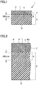
- Fig. 1 is a schematic cross-sectional view of the diamond joined body of the present disclosure.
- Fig. 2 is a schematic cross-sectional view of a region near an interface between a hard substrate and a polycrystalline diamond layer of the diamond joined body of the present disclosure.
- a diamond joined body 1 includes a hard substrate 3 and a polycrystalline diamond layer 2 arranged on hard substrate 3.
- An area ratio of carbon grains in a region (hereinafter, also denoted as "region A") of hard substrate 3 is less than 0.03%, the region being a region enclosed by an interface P between hard substrate 3 and polycrystalline diamond layer 2 and an imaginary line x in a cross section parallel to a normal direction of interface P, imaginary line x being parallel to interface P on the hard substrate side and having a distance of 500 ⁇ m from interface P.
- a tool including the diamond joined body can have an improved chipping resistance and a long tool life. Although the reason for this is not exactly known, the present inventors make the following inference.
- the carbon grains present in the hard substrate are precipitated carbon grains including at least one of grains composed of, for example, amorphous carbon, graphite or diamond.
- a region including the precipitated carbon grains and the neighborhood thereof has a low strength, and thus, the region tends to become the origin of a crack.
- a tool produced using the diamond joined body in which the precipitated carbon grains are present is inferior in chipping resistance to a breakage originating from the hard substrate during use of the tool, and thus, the tool tends to have a short tool life.
- an area ratio of the precipitated carbon grains in region A in the hard substrate is less than 0.03%. That is, an amount of the precipitated carbon grains in the hard substrate is sufficiently small, and thus, the occurrence of a crack is suppressed.
- the above-described area ratio of the precipitated carbon grains in the hard substrate is calculated in accordance with the following procedure of (a) to (d).
- diamond joined body 1 is cut in a direction vertical to a surface of diamond joined body 1, i.e., a surface of polycrystalline diamond layer 2, to thereby obtain an exposed cross section.
- the exposed cross section is mirror-polished using diamond slurry having an average grain size of 3 ⁇ m.
- hard substrate 3 is produced such that a surface of hard substrate 3 is as smooth as possible, and polycrystalline diamond layer 2 is formed on hard substrate 3 such that a thickness of polycrystalline diamond layer 2 is uniform. Therefore, even when the surface of hard substrate 3 (interface with polycrystalline diamond layer 2) is somewhat uneven, the surface of polycrystalline diamond layer 2 becomes substantially parallel to interface P, and thus, there is no influence on the accuracy of measurement of the area ratio of the carbon grains described below.
- a plane that is parallel to a reference plane PS which is a plane having an average height of an actual interface P', and passes through a tip of a recessed portion of actual interface P' recessed most toward the hard substrate side is defined as interface P.
- "area of hard substrate 3 protruding from reference plane PS to the polycrystalline diamond layer 2 side” is identical to "area of polycrystalline diamond layer 2 protruding from reference plane PS to the hard substrate 3 side”.
- interface P is parallel to a main surface T on the surface side of polycrystalline diamond layer 2 and a main surface Q on the surface side of hard substrate 3.
- a normal line of interface P is identical to a normal line of main surface T on the surface side of polycrystalline diamond layer 2 and a normal line of main surface Q on the surface side of hard substrate 3.
- an image of each measurement field of view is captured under the following conditions.
- optical microscope "AXIO Vert.A1" (product name) manufactured by Carl Zeiss AG lens: "EC Epiplan 100x/0.85 HD M27” (product name) manufactured by Carl Zeiss AG conditions for capturing images: time: 700 ms, intensity: 80%, gamma: 0.45
- image processing software Win Roof ver.7.4.5 process procedure:
- An area ratio of pixels derived from a bright field of view (pixels derived from the carbon grains) to an area of the measurement field of view (hard substrate), i.e., the area ratio of the carbon grains in the measurement field of view is calculated from the images obtained in (c) above.
- an area ratio of carbon grains in a region of the hard substrate is less than 0.03%, the region being a region enclosed by an interface between the polycrystalline diamond layer and the hard substrate and an imaginary line x in a cross section parallel to a normal direction of a main surface of the hard substrate, the imaginary line x being parallel to the interface and having a distance of 500 ⁇ m from the interface” means that the area ratios of the carbon grains in the five measurement fields of view are all less than 0.03%.
- the area ratio of the carbon grains is preferably not more than 0.02%, and more preferably not more than 0.01%.
- the smaller area ratio of the carbon grains is more preferable, and thus, a lower limit value is 0%. Therefore, the area ratio of the carbon grains can also be defined as not less than 0% and less than 0.03%.
- WC-based cemented carbide including tungsten carbide (hereinafter, also denoted as "WC") as a base material can be used as hard substrate 3.
- Such hard substrate 3 can have a high hardness and a high strength.
- a thickness (vertical direction in Fig. 1 ) of hard substrate 3 is not particularly limited, and can be, for example, not less than 1 mm and not more than 30 mm.
- Hard substrate 3 preferably includes tungsten carbide grains (hereinafter, also denoted as "WC grains") having a volume average grain size of not less than 0.1 ⁇ m and not more than 3 ⁇ m.
- WC grains tungsten carbide grains
- a fracture toughness of the WC-based cemented carbide tends to become lower as the grain size of the WC grains forming the WC-based cemented carbide becomes smaller (e.g., volume average grain size of not less than 0.1 ⁇ m and not more than 3 ⁇ m).
- WC-based cemented carbide including the WC grains having a grain size of not more than 3 ⁇ m has not been conventionally selected as a material of the hard substrate.
- a transverse-rupture-strength (TRS) of the WC-based cemented carbide becomes higher as the grain size of the WC grains forming the WC-based cemented carbide becomes smaller. Therefore, if there is no origin of the occurrence of a crack (fracture origin), the WC-based cemented carbide including the WC grains having a small grain size has properties of high transverse-rupture-strength and being hard-to-break.
- the area ratio of the carbon grains that may become the origin of a crack is less than 0.03% and the amount of the carbon grains is sufficiently small, and thus, the origin of the occurrence of a crack is also sufficiently reduced.
- the volume average grain size of the WC grains is not less than 0.1 ⁇ m and not more than 3 ⁇ m in the hard substrate, the transverse-rupture-strength of the hard substrate is high, and the origin of the occurrence of a crack is also sufficiently reduced. Therefore, a tool including the hard substrate is less likely to become cracked and can have a longer tool life.
- the WC grains can take in a larger amount of carbon precipitated from the polycrystalline diamond layer to the hard substrate side during sintering.
- the precipitated carbon taken into the WC grains is present between the WC grains or in a binder phase as tungsten carbide or carbide of another element (such as V or Co) included in the hard substrate, and is not present in the form of the carbon grains.
- volume average grain size of the WC grains refers to a median size (d50) in a volume-based grain size distribution (volume distribution), and refers to an average grain size targeted at all WC grains included in the hard substrate.
- volume average grain size may also be denoted simply as “grain size”.
- a grain size of each grain for calculating the grain size (volume average grain size) of the WC grains can be measured in accordance with the following method.
- the hard substrate is cut using the wire electric discharge processing machine, to thereby obtain a cut surface.
- the cut surface is mirror-polished, to thereby obtain a polished surface.
- a measurement field of view of 100 ⁇ m ⁇ 100 ⁇ m is arbitrarily set to include a region distant by 600 ⁇ m toward the hard substrate side from interface P between the hard substrate and the polycrystalline diamond layer.
- a reflected electron image of the measurement field of view is observed at 5000x magnification, using an electron microscope ("SU6600" manufactured by HITACHI).
- a diameter of a circle circumscribing the WC grains i.e., circumscribed circle equivalent diameter
- the diameter is defined as the grain size of the WC grains.
- a content of the WC grains in the hard substrate is preferably not less than 70 mass% and less than 100 mass%, more preferably not less than 70 mass% and not more than 90 mass%, and further preferably not less than 81 mass% and not more than 88 mass%.
- the content (mass%) of the WC grains in the hard substrate is calculated in accordance with the following method.
- the hard substrate is cut using the wire electric discharge processing machine, to thereby obtain a cut surface.
- the cut surface is mirror-polished using diamond slurry having an average grain size of 3 ⁇ m, to thereby produce a sample for observation.
- a measurement field of view of 100 ⁇ m ⁇ 100 ⁇ m is arbitrarily set on the polished surface of the sample for observation, and the measurement field of view is subjected to energy dispersive X-ray spectroscopy ("X-Max" manufactured by Oxford Instruments) to measure the content (mass%) of the WC grains.
- X-Max energy dispersive X-ray spectroscopy
- hard substrate 3 includes preferably not less than 0.01 mass% and not more than 2.0 mass%, more preferably not less than 0.05 mass% and not more than 1 mass%, and further preferably not less than 0.1 mass% and not more than 0.5 mass%, in total of at least one type of element selected from the group consisting of Ta (tantalum), Cr (chromium) and V (vanadium).
- Hard substrate 3 is produced by sintering the WC grains as a raw material (hereinafter, also denoted as "raw material WC grains"), together with iron-based metal.
- raw material WC grains a raw material
- iron-based metal iron-based metal
- Ta, Cr and V in the hard substrate bond with carbon that has moved from the polycrystalline diamond layer, to thereby generate carbide such as TaC (tantalum carbide), Cr 3 C 2 (chromium carbide) or CV (vanadium carbide). Therefore, when at least one of Ta, Cr and V is present in the hard substrate, precipitation of carbon is suppressed.
- carbide such as TaC (tantalum carbide), Cr 3 C 2 (chromium carbide) or CV (vanadium carbide). Therefore, when at least one of Ta, Cr and V is present in the hard substrate, precipitation of carbon is suppressed.
- hard substrate 3 includes preferably not less than 11 mass% and not more than 20 mass%, more preferably not less than 11 mass% and not more than 17 mass%, and further preferably not less than 11 mass% and not more than 15 mass%, of Co (cobalt).
- a content of Co in the hard substrate is not less than 11 mass%, a thermal expansion coefficient of the cemented carbide forming the hard substrate tends to increase, and thus, a difference in thermal expansion coefficient between the hard substrate and the polycrystalline diamond layer tends to increase.
- the hard substrate and the polycrystalline diamond layer are sintered and joined in a state where a raw material powder of the polycrystalline diamond layer is arranged on the hard substrate. Therefore, when the difference in thermal expansion coefficient between the hard substrate and the polycrystalline diamond layer is large, a large residual stress occurs in the hard substrate and the polycrystalline diamond layer subjected to sintering.
- a tensile stress occurs in the direction parallel to the interface
- a compressive stress occurs in the direction parallel to the interface. Due to this, a crack originating from the hard substrate side of the interface is likely to occur, and a crack may occur after ultra-high-pressure sintering and/or a breakage originating from the hard substrate side of the interface may occur during use as a tool. Therefore, not less than 11 mass% has not been conventionally selected as the content of Co in the hard substrate.
- the present inventors have newly found that, when the amount of the carbon grains is sufficiently reduced in the hard substrate near the interface between the hard substrate and the polycrystalline diamond layer, the hard substrate has an excellent fracture toughness value, even if the content of Co in the hard substrate is not less than 11 mass%. Although the reason for this is not exactly known, it is estimated that the amount of the carbon grains that becomes the origin of a crack is sufficiently reduced near the interface, and thus, the hard substrate used in the present embodiment has high resistance to a crack and the occurrence of a crack caused by an increase in residual stress with an increase in Co can be suppressed. A tool including the hard substrate is less likely to become cracked and can have a longer tool life.
- hard substrate 3 may include Fe (iron) and Ni (nickel). It is preferable that hard substrate 3 does not include Re. Since Re is expensive, hard substrate 3 that does not include Re has a cost advantage.
- a content (mass%) of each of Ta, Cr, V, and Co in the hard substrate is calculated in accordance with the following method.
- the hard substrate is cut using the wire electric discharge processing machine, to thereby obtain a cut surface.
- the cut surface is mirror-polished using diamond slurry having an average grain size of 3 ⁇ m, to thereby produce a sample for observation.
- a measurement field of view of 100 ⁇ m ⁇ 100 ⁇ m is arbitrarily set on the polished surface of the sample for observation, and the measurement field of view is subjected to energy dispersive X-ray spectroscopy ("X-Max" manufactured by Oxford Instruments) to measure a mass ratio of each element.
- X-Max energy dispersive X-ray spectroscopy
- a so-called polycrystalline diamond sintered body obtained by sintering diamond grains through the use of a sintering aid can be used as polycrystalline diamond layer 2.
- Polycrystalline diamond layer 2 can include unavoidable impurities, in addition to the diamond grains and the sintering aid.
- a content of the diamond grains in polycrystalline diamond layer 2 is preferably not less than 70 volume% and not more than 98 volume%, and more preferably not less than 80 volume% and not more than 98 volume%.
- the content of the diamond grains is less than 70 volume%, the hardness of polycrystalline diamond layer 2 may be insufficient.
- the content of the diamond grains is more than 98 volume%, a content of the sintering aid decreases relatively, which makes bonding between the diamond grains weak or makes a degree of bonding nonuniform.
- the content of the sintering aid in polycrystalline diamond layer 2 is preferably more than 2 volume% and less than 30 volume%.
- the content of the sintering aid is low, which makes bonding between the diamond grains weak or makes a degree of bonding nonuniform.
- the content of the sintering aid is not less than 30 volume%, the hardness of polycrystalline diamond layer 2 may be insufficient.
- the content of the diamond grains in polycrystalline diamond layer 2 is calculated in accordance with the following method.
- the polycrystalline diamond layer is cut using the wire electric discharge processing machine, to thereby obtain a cut surface.
- the cut surface is mirror-polished, to thereby obtain a polished surface.
- a measurement field of view of 100 ⁇ m ⁇ 100 ⁇ m is arbitrarily set to include a region distant by 200 ⁇ m toward the polycrystalline diamond layer side from interface P between the hard substrate and the polycrystalline diamond layer.
- a reflected electron image of the measurement field of view is observed at 5000x magnification, using the electron microscope.
- a diamond phase composed of the diamond grains is observed as a black region, and a binder phase composed of the sintering aid is observed as a gray region or a white region.
- the diamond phase region and the binder phase region are binarized by image processing, to thereby measure an occupancy area of the diamond phase region.
- the occupancy area is substituted into the following equation (1), to thereby calculate a volume content of the diamond grains.
- volume content of diamond phase occupancy area of diamond phase region ⁇ area of polycrystalline diamond layer 2 in field-of-view image ⁇ 100
- the thickness (vertical direction in Fig. 1 ) of polycrystalline diamond layer 2 is not particularly limited, and can be, for example, not less than 0.1 mm and not more than 5 mm.
- the diamond grains preferably have a volume average grain size of not less than 0.1 ⁇ m and not more than 50 ⁇ m.
- the volume average grain size of the diamond grains is more than 50 ⁇ m, a defect caused by cleavage of the diamond grains themselves is likely to occur.
- chipping is likely to occur in polycrystalline diamond layer 2.
- the grains having a volume average grain size of less than 0.1 ⁇ m are difficult to manufacture and handling thereof is also complicated.
- the volume average grain size of the diamond grains is more preferably not less than 0.1 ⁇ m and not more than 30 ⁇ m, and further preferably not less than 0.1 ⁇ m and not more than 5 ⁇ m.
- volume average grain size of the diamond grains refers to a median size (d50) in a volume-based grain size distribution (volume distribution), and refers to an average grain size targeted at all diamond grains included in the polycrystalline diamond layer.
- a grain size of each grain for calculating the grain size (volume average grain size) of the diamond grains can be measured in accordance with the following method.
- a cross section of polycrystalline diamond layer 2 is mirror-polished, to thereby obtain a polished surface.
- a measurement field of view of 100 ⁇ m ⁇ 100 ⁇ m is arbitrarily set to include a region distant by 200 ⁇ m toward the polycrystalline diamond layer side from interface P between the hard substrate and the polycrystalline diamond layer.
- a reflected electron image of the measurement field of view is observed at 5000x magnification, using the electron microscope.
- a diameter of a circle circumscribing the grains forming the diamond phase i.e., circumscribed circle equivalent diameter
- the diameter is defined as the grain size of the diamond grains.
- the diamond grains may be present individually, or may be present in a state where adjacent grains are bonded, i.e., in a state where neck growth is formed. However, in order to obtain polycrystalline diamond layer 2 having a higher strength, it is preferable that 90 volume% or more of the diamond grains forming the diamond phase are present in a state where neck growth is formed. Whether the diamond grains are present individually or in a state where neck growth is formed, and a volume% thereof can be controlled depending on a type and an amount of addition of the sintering aid described below.
- the sintering aid can include known sintering aids used as sintering aids of diamond grains.
- examples can include iron group metal such as cobalt (Co), iron (Fe) and nickel (Ni), titanium (Ti), zirconium (Zr), hafnium (Hf), vanadium (V), niobium (Nb), tantalum (Ta), chromium (Cr), molybdenum (Mo), tungsten (W), and manganese (Mn).
- Co is suitably used as the sintering aid of the diamond grains, because of its high rate of dissolution precipitation reaction of the diamond grains that drives neck growth formation of the diamond grains.
- a content of Co in polycrystalline diamond layer 2 is preferably not less than 2 volume% and not more than 30 volume%.
- the content of Co in polycrystalline diamond layer 2 is less than 2 volume%, bonding between the diamond grains tends to be weak or a degree of bonding tends to be nonuniform.
- the content of Co in polycrystalline diamond layer 2 is more than 30 volume%, the wear resistance and the strength such as chipping resistance and impact resistance of polycrystalline diamond layer 2 decrease.
- the sintering aid includes one or more of the above-described elements other than Co
- contents of the elements other than Co in a binder in polycrystalline diamond layer 2 are preferably not less than 0.1 volume% and not more than 80 volume%.
- the content of Co in polycrystalline diamond layer 2 can be calculated in accordance with the following method.
- the polycrystalline diamond layer is cut using the wire electric discharge processing machine, to thereby obtain a cut surface.
- the cut surface is mirror-polished, to thereby obtain a polished surface.
- a measurement field of view of 100 ⁇ m ⁇ 100 ⁇ m is arbitrarily set to include a region distant by 200 ⁇ m toward the polycrystalline diamond layer side from interface P between the hard substrate and the polycrystalline diamond layer.
- a reflected electron image of the measurement field of view is observed at 5000x magnification, using the electron microscope.
- the diamond phase composed of the diamond grains is observed as a black region, and the binder phase composed of the sintering aid is observed as a gray region or a white region.
- the diamond phase region and the binder phase region are binarized by image processing, to thereby measure an occupancy area of the binder phase region.
- the occupancy area is substituted into the following equation (2), to thereby calculate a volume content of Co.
- volume content of Co occupancy area of binder phase region ⁇ area of polycrystalline diamond phase in field-of-view image ⁇ 100
- the content (mass%) of each of Co and the other elements can be calculated by ICP analysis.
- Polycrystalline diamond layer 2 may include a cobalt-rich layer having a prescribed thickness from the interface side with hard substrate 3 and showing a high content (volume%) of cobalt.
- polycrystalline diamond layer 2 includes the cobalt-rich layer, the residual stress caused by the difference in thermal expansion coefficient between polycrystalline diamond layer 2 and hard substrate 3 can be reduced.
- the diamond joined body according to the present embodiment can be used in, for example, a cutting tool such as a drill, an end mill, an indexable cutting insert for milling, an indexable cutting insert for turning, a metal saw, a gear cutting tool, a reamer, or a tap, a wear-resistant tool such as a dresser, a stylus, a nozzle, or a dice, a grinding tool such as a grindstone, a wire saw, a blade, or a bit, and a tool such as a tool for friction stir welding.
- a tool produced using the diamond joined body can have an improved chipping resistance and a long tool life.
- the method for manufacturing the diamond joined body according to the present embodiment is a method for manufacturing the diamond joined body according to the first embodiment, the method including: preparing a hard substrate including tungsten carbide grains having a volume average grain size of not less than 0.1 ⁇ m and not more than 3 ⁇ m (hereinafter, also denoted as “hard substrate preparation step”); producing a compact by arranging a polycrystalline diamond layer raw material powder on the hard substrate (hereinafter, also denoted as “compact production step”); and sintering the compact under pressure and temperature conditions in which diamond is stable, to thereby obtain a diamond joined body (hereinafter, also denoted as "sintering step”).
- a hard substrate including tungsten carbide grains having a volume average grain size of not less than 0.1 ⁇ m and not more than 3 ⁇ m is prepared.
- a compact is produced by arranging a polycrystalline diamond layer raw material powder on the hard substrate.
- the polycrystalline diamond layer raw material powder can be obtained by mixing diamond grains and a sintering aid using a ball mill or the like.
- a grain size of the diamond grains in the polycrystalline diamond layer raw material powder can be calculated based on a grain size distribution measured in accordance with a laser diffraction method.
- the details of the sintering aid used in this step is similar to the sintering aid described in detail in the first embodiment, and thus, description thereof will not be repeated.
- Examples of a method for arranging the polycrystalline diamond layer raw material powder on the hard substrate include a method for arranging a preliminarily sintered hard substrate in a mold made of a high heat-resistant material such as tantalum, and arranging a polycrystalline diamond layer raw material powder on the hard substrate in a layered manner with a prescribed thickness. A compact can thus be obtained.
- one layer is molded using the mixed powder obtained by mixing the diamond grains and the sintering aid using the ball mill or the like.
- the diamond grains and the sintering aid may be molded in different layers.
- a sintered body having a degree of neck growth that is uniform all over the sintered body is obtained.
- the sintering aid and the diamond grains are molded in two different layers, a sintered body having a layer including the diamond grains at high density is obtained.
- Such a sintered body is excellent in strength and wear resistance.
- the obtained compact is sintered under pressure and temperature conditions in which diamond is stable.
- the pressure and temperature conditions in which diamond is stable refers to the conditions that the pressure is not less than 5.0 GPa and not more than 8.0 GPa and the temperature is not less than 1300°C and not more than 1900°C.
- the sintering time is not particularly limited, and is changed as appropriate depending on the size, thickness and the like of the compact. However, by sintering the compact for at least 5 minutes or longer, a sufficiently sintered diamond joined body can be obtained.
- a hard substrate including 88 mass% of WC grains having a volume average grain size of 0.3 ⁇ m was prepared.
- the hard substrate includes 0.4 mass% in total of Ta, Cr and V.
- a hard substrate including 92.2 mass% of WC grains having a volume average grain size of 5 ⁇ m was prepared.
- the hard substrate does not include Ta, Cr and V.
- Diamond grains having a volume average grain size of 5 ⁇ m and Co grains were mixed to prepare a polycrystalline diamond layer raw material powder.
- a content of the diamond grains in the polycrystalline diamond layer raw material powder was 96 mass%, and a content of the Co grains was 4 mass%.
- the hard substrate of each sample and the polycrystalline diamond layer raw material powder were arranged in this order in a mold made of tantalum, to thereby obtain a compact.
- a Co content (mass%) in the hard substrate was measured by analysis using energy dispersive X-ray spectroscopy. A specific measurement method is described in the first embodiment, and thus, description thereof will not be repeated. The results are shown in the column of "Co content (mass%)" in Table 1.
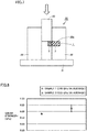
- a diamond joined body test piece having a prescribed size was cut from the diamond joined body of each sample. Then, using a shear tester 20 shown in Fig. 7 , a shear strength of the diamond joined body test piece was measured. Specifically, for each diamond joined body test piece, shear tester 20 was fixed such that hard substrate 3 was located in a holding portion 22a and polycrystalline diamond layer 2 was reliably exposed from holding portion 22a. For each test piece, care was taken so that the equivalent region was located in holding portion 22a. Then, a head 23 was pressed against each test piece to apply a load, and a load at which each test piece was broken was defined as a shear strength of each diamond joined body. The shear test was performed four times on each sample. The higher shear strength indicates that a crack is less likely to occur and the chipping resistance is more excellent. The results are shown in Fig. 8 .
- Sample 1 the area ratio of the precipitated carbon is 0%, and Sample 1 corresponds to Example.
- Sample 2 the area ratio of the precipitated carbon is 0.49%, and Sample 2 corresponds to Comparative Example. It was confirmed that Sample 1 was higher in shear strength and more excellent in chipping resistance than Sample 2.
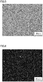
- FIG. 3 An optical micrograph of a measurement field of view of a cross section of the diamond joined body of Sample 1 (Example) is shown in Fig. 3 . As shown in Fig. 3 , the precipitated carbon was not seen in the region of the hard substrate in Sample 1.
- Fig. 4 is a binarized image of the optical micrograph shown in Fig. 3 . In Fig. 4 as well, the precipitated carbon was not seen.
- the diamond joined body test piece of Sample 1 subjected to the shear test was observed. Only the hard substrate had a crack, and the polycrystalline diamond layer did not have a crack. Therefore, it was confirmed that the diamond joined body of Sample 1 had an improved chipping resistance to a breakage originating from the hard substrate during use of the tool.
- FIG. 5 An optical micrograph of a measurement field of view of a cross section of the diamond joined body of Sample 2 (Comparative Example) is shown in Fig. 5 .
- the precipitated carbon was seen in the region of the hard substrate in Sample 2.
- Fig. 6 is a binarized image of the optical micrograph shown in Fig. 5 .
- the precipitated carbon was seen.
Landscapes
- Engineering & Computer Science (AREA)
- Mechanical Engineering (AREA)
- Chemical & Material Sciences (AREA)
- Materials Engineering (AREA)
- Manufacturing & Machinery (AREA)
- Organic Chemistry (AREA)
- Metallurgy (AREA)
- Composite Materials (AREA)
- Ceramic Engineering (AREA)
- Life Sciences & Earth Sciences (AREA)
- Wood Science & Technology (AREA)
- Cutting Tools, Boring Holders, And Turrets (AREA)
- Carbon And Carbon Compounds (AREA)
- Crystals, And After-Treatments Of Crystals (AREA)
- Laminated Bodies (AREA)
Abstract
Description
- The present disclosure relates to a diamond joined body and a method for manufacturing the diamond joined body. The present application claims the priority to Japanese Patent Application No.
2018-116201 filed on June 19, 2018 - Diamond has an extremely high hardness, and sintered polycrystalline diamond bodies manufactured from diamond grains as a raw material are used in a variety of tools such as cutting tools, wear-resistant tools, etc.
- When a sintered polycrystalline diamond body is used in a tool, the sintered polycrystalline diamond body is generally used by joining a joined body obtained by joining the sintered polycrystalline diamond body to a hard substrate (hereinafter also denoted as a "diamond joined body") to a base metal serving as the base body of the tool.
- Japanese Patent Laying-Open No.
2010-208942 -
- PTL 1: Japanese Patent Laying-Open No.
2010-208942 - PTL 2: Japanese National Patent Publication No.
2016-513177 -
- [1] A diamond joined body of the present disclosure is a diamond joined body including a hard substrate and a polycrystalline diamond layer arranged on the hard substrate, wherein
an area ratio of carbon grains in a region of the hard substrate is less than 0.03%, the region being a region enclosed by an interface between the hard substrate and the polycrystalline diamond layer and an imaginary line x in a cross section parallel to a normal direction of the interface, the imaginary line x being parallel to the interface on the hard substrate side and having a distance of 500 µm from the interface. - [2] A method for manufacturing the diamond joined body of the present disclosure is a method for manufacturing the diamond joined body as recited in [1] above, the method comprising:
- preparing a hard substrate including tungsten carbide grains having a volume average grain size of not less than 0.1 µm and not more than 3 µm;
- producing a compact by arranging a polycrystalline diamond layer raw material powder on the hard substrate; and
- sintering the compact under pressure and temperature conditions in which diamond is stable, to thereby obtain a diamond joined body.
-
-
Fig. 1 is a schematic cross-sectional view of a diamond joined body of the present disclosure. -
Fig. 2 is a schematic cross-sectional view of a region near an interface between a hard substrate and a polycrystalline diamond layer of the diamond joined body of the present disclosure. -
Fig. 3 is an optical micrograph of a measurement field of view of a diamond joined body of Sample 1 (Example). -
Fig. 4 is a binarized image of the optical micrograph shown inFig. 3 . -
Fig. 5 is an optical micrograph of a measurement field of view of a diamond joined body of Sample 2 (Comparative Example). -
Fig. 6 is a binarized image of the optical micrograph shown inFig. 5 . -
Fig. 7 is a schematic cross-sectional view of a shear tester used in a shear test. -
Fig. 8 is a graph showing results of the shear test. - A diamond joined body produced in accordance with a conventional manufacturing method has had such a tendency that carbon diffuses from diamond to the hard substrate side during sintering and is precipitated in the hard substrate. Since a region including the precipitated carbon and the neighborhood thereof has a low strength, the region tends to become the origin of a crack. Therefore, there is a demand for a technique of suppressing the precipitation of carbon in the hard substrate in the diamond joined body.
- Japanese National Patent Publication No.
2016-513177 PTL 2 defines that the substrate does not substantially contain free carbon, Re is very expensive, and thus, it has been difficult to put the polycrystalline superhard structure to practical use. - The present disclosure has been made to solve the above-described problem and an object of the present disclosure is to provide a diamond joined body in which precipitation of carbon in a hard substrate is suppressed, and a method for manufacturing the diamond joined body.
- In the diamond joined body of the present disclosure, precipitation of carbon in the hard substrate is suppressed. Therefore, a tool including the diamond joined body can have an improved chipping resistance to a breakage originating from the hard substrate during use of the tool, and a long tool life.
- According to the method for manufacturing the diamond joined body of the present disclosure, there can be obtained a diamond joined body in which precipitation of carbon to the hard substrate side is suppressed.
- First, embodiments of the present disclosure are listed below.
- (1) A diamond joined body of the present disclosure is a diamond joined body including a hard substrate and a polycrystalline diamond layer arranged on the hard substrate, wherein
an area ratio of carbon grains in a region of the hard substrate is less than 0.03%, the region being a region enclosed by an interface between the hard substrate and the polycrystalline diamond layer and an imaginary line x in a cross section parallel to a normal direction of the interface, the imaginary line x being parallel to the interface on the hard substrate side and having a distance of 500 µm from the interface.
In the diamond joined body, precipitation of carbon in the hard substrate is suppressed. Therefore, a tool including the diamond joined body can have an improved chipping resistance to a breakage originating from the hard substrate during use of the tool, and a long tool life. - (2) Preferably, the hard substrate includes tungsten carbide grains having a volume average grain size of not less than 0.1 µm and not more than 3 µm. Thus, precipitation of carbon in the hard substrate is further suppressed.
- (3) Preferably, the hard substrate includes not less than 70 mass% of the tungsten carbide grains and includes less than 100 mass% of the tungsten carbide grains. Thus, precipitation of carbon in the hard substrate is further suppressed.
- (4) Preferably, the hard substrate includes not less than 0.01 mass% and not more than 2.0 mass% in total of at least one type of element selected from the group consisting of Ta, Cr and V. Thus, grain growth of tungsten grains forming the hard substrate can be suppressed. Therefore, a grain size of a raw material tungsten grains is likely to be maintained as a grain size of the tungsten grains in the hard substrate.
- (5) Preferably, the hard substrate includes not less than 11 mass% and not more than 15 mass% of Co. Thus, a fracture toughness value of the hard substrate is improved, and a tool including the hard substrate is less likely to become cracked and can have a longer tool life.
- (6) A method for manufacturing the diamond joined body of the present disclosure is a method for manufacturing the diamond joined body as recited in any one of (1) to (5) above, the method comprising:
- preparing a hard substrate including tungsten carbide grains having a volume average grain size of not less than 0.1 µm and not more than 3 µm;
- producing a compact by arranging a polycrystalline diamond layer raw material powder on the hard substrate; and
- sintering the compact under pressure and temperature conditions in which diamond is stable, to thereby obtain a diamond joined body.
- According to the manufacturing method, there can be obtained a diamond joined body in which precipitation of carbon in the hard substrate is suppressed.
- Specific examples of the diamond joined body of the present disclosure and the method for manufacturing the same will be described below with reference to the figures. The present disclosure is not limited to these examples, and is defined by the terms of the claims and is intended to include any modifications within the scope and meaning equivalent to the terms of the claims.
- The diamond joined body of the present disclosure will be described with reference to
Figs. 1 and 2. Fig. 1 is a schematic cross-sectional view of the diamond joined body of the present disclosure.Fig. 2 is a schematic cross-sectional view of a region near an interface between a hard substrate and a polycrystalline diamond layer of the diamond joined body of the present disclosure. - As shown in
Fig. 1 , a diamond joinedbody 1 includes ahard substrate 3 and apolycrystalline diamond layer 2 arranged onhard substrate 3. - An area ratio of carbon grains in a region (hereinafter, also denoted as "region A") of
hard substrate 3 is less than 0.03%, the region being a region enclosed by an interface P betweenhard substrate 3 andpolycrystalline diamond layer 2 and an imaginary line x in a cross section parallel to a normal direction of interface P, imaginary line x being parallel to interface P on the hard substrate side and having a distance of 500 µm from interface P. A tool including the diamond joined body can have an improved chipping resistance and a long tool life. Although the reason for this is not exactly known, the present inventors make the following inference. - The carbon grains present in the hard substrate are precipitated carbon grains including at least one of grains composed of, for example, amorphous carbon, graphite or diamond. When the precipitated carbon grains are present in the hard substrate, a region including the precipitated carbon grains and the neighborhood thereof has a low strength, and thus, the region tends to become the origin of a crack. A tool produced using the diamond joined body in which the precipitated carbon grains are present is inferior in chipping resistance to a breakage originating from the hard substrate during use of the tool, and thus, the tool tends to have a short tool life.
- In diamond joined
body 1 according to the present embodiment, an area ratio of the precipitated carbon grains in region A in the hard substrate is less than 0.03%. That is, an amount of the precipitated carbon grains in the hard substrate is sufficiently small, and thus, the occurrence of a crack is suppressed. - The above-described area ratio of the precipitated carbon grains in the hard substrate is calculated in accordance with the following procedure of (a) to (d).
- Using a wire electric discharge processing machine, diamond joined
body 1 is cut in a direction vertical to a surface of diamond joinedbody 1, i.e., a surface ofpolycrystalline diamond layer 2, to thereby obtain an exposed cross section. The exposed cross section is mirror-polished using diamond slurry having an average grain size of 3 µm. In the present embodiment,hard substrate 3 is produced such that a surface ofhard substrate 3 is as smooth as possible, andpolycrystalline diamond layer 2 is formed onhard substrate 3 such that a thickness ofpolycrystalline diamond layer 2 is uniform. Therefore, even when the surface of hard substrate 3 (interface with polycrystalline diamond layer 2) is somewhat uneven, the surface ofpolycrystalline diamond layer 2 becomes substantially parallel to interface P, and thus, there is no influence on the accuracy of measurement of the area ratio of the carbon grains described below. - In the cross section of diamond joined
body 1, five measurement fields of view each having a rectangular shape with a width (direction parallel to interface P) of 120 µm × a height (direction vertical to interface P) of 100 µm are selected randomly in region A enclosed by interface P and imaginary line x, imaginary line x being parallel to interface P on thehard substrate 3 side and having a distance of 500 µm from above-described interface P. - As measured by the applicant, it has been confirmed that, for measurement in the same sample, while a location where a measurement field of view is selected is changed and calculation is performed for a plurality of times, measurement results of the area ratio of the carbon grains described below are obtained without substantial variations.
- As shown in
Fig. 2 , a plane that is parallel to a reference plane PS, which is a plane having an average height of an actual interface P', and passes through a tip of a recessed portion of actual interface P' recessed most toward the hard substrate side is defined as interface P. In the above-described cross section, "area ofhard substrate 3 protruding from reference plane PS to thepolycrystalline diamond layer 2 side" is identical to "area ofpolycrystalline diamond layer 2 protruding from reference plane PS to thehard substrate 3 side". - In
Figs. 1 and 2 , interface P is parallel to a main surface T on the surface side ofpolycrystalline diamond layer 2 and a main surface Q on the surface side ofhard substrate 3. In this case, a normal line of interface P is identical to a normal line of main surface T on the surface side ofpolycrystalline diamond layer 2 and a normal line of main surface Q on the surface side ofhard substrate 3. - Using the following devices, an image of each measurement field of view is captured under the following conditions.
- optical microscope: "AXIO Vert.A1" (product name) manufactured by Carl Zeiss AG
lens: "EC Epiplan 100x/0.85 HD M27" (product name) manufactured by Carl Zeiss AG
conditions for capturing images: time: 700 ms, intensity: 80%, gamma: 0.45 - Using the following image processing software, binarization processing is performed on the images captured in (b) above in accordance with the following procedure.
image processing software: Win Roof ver.7.4.5
process procedure: - 1. correction of histogram average brightness (correction reference value: 128)
- 2. background subtraction (object size: 30 µm)
- 3. binarization with single threshold value (threshold value: 100)
- 4. brightness reversal (only a region of the carbon grains is extracted)
- An area ratio of pixels derived from a bright field of view (pixels derived from the carbon grains) to an area of the measurement field of view (hard substrate), i.e., the area ratio of the carbon grains in the measurement field of view is calculated from the images obtained in (c) above.
- In the present embodiment, "an area ratio of carbon grains in a region of the hard substrate is less than 0.03%, the region being a region enclosed by an interface between the polycrystalline diamond layer and the hard substrate and an imaginary line x in a cross section parallel to a normal direction of a main surface of the hard substrate, the imaginary line x being parallel to the interface and having a distance of 500 µm from the interface" means that the area ratios of the carbon grains in the five measurement fields of view are all less than 0.03%.
- The area ratio of the carbon grains is preferably not more than 0.02%, and more preferably not more than 0.01%. The smaller area ratio of the carbon grains is more preferable, and thus, a lower limit value is 0%. Therefore, the area ratio of the carbon grains can also be defined as not less than 0% and less than 0.03%.
- So-called WC-based cemented carbide including tungsten carbide (hereinafter, also denoted as "WC") as a base material can be used as
hard substrate 3. Suchhard substrate 3 can have a high hardness and a high strength. In diamond joinedbody 1, a thickness (vertical direction inFig. 1 ) ofhard substrate 3 is not particularly limited, and can be, for example, not less than 1 mm and not more than 30 mm. -
Hard substrate 3 preferably includes tungsten carbide grains (hereinafter, also denoted as "WC grains") having a volume average grain size of not less than 0.1 µm and not more than 3 µm. Generally, a fracture toughness of the WC-based cemented carbide tends to become lower as the grain size of the WC grains forming the WC-based cemented carbide becomes smaller (e.g., volume average grain size of not less than 0.1 µm and not more than 3 µm). When such WC-based cemented carbide is used as a tool material, a crack is likely to occur in the tool. Therefore, the WC-based cemented carbide including the WC grains having a grain size of not more than 3 µm has not been conventionally selected as a material of the hard substrate. - In contrast, a transverse-rupture-strength (TRS) of the WC-based cemented carbide becomes higher as the grain size of the WC grains forming the WC-based cemented carbide becomes smaller. Therefore, if there is no origin of the occurrence of a crack (fracture origin), the WC-based cemented carbide including the WC grains having a small grain size has properties of high transverse-rupture-strength and being hard-to-break.
- In the hard substrate used in the present embodiment, the area ratio of the carbon grains that may become the origin of a crack is less than 0.03% and the amount of the carbon grains is sufficiently small, and thus, the origin of the occurrence of a crack is also sufficiently reduced. When the volume average grain size of the WC grains is not less than 0.1 µm and not more than 3 µm in the hard substrate, the transverse-rupture-strength of the hard substrate is high, and the origin of the occurrence of a crack is also sufficiently reduced. Therefore, a tool including the hard substrate is less likely to become cracked and can have a longer tool life.
- Furthermore, as the grain size of the WC grains becomes smaller, the WC grains can take in a larger amount of carbon precipitated from the polycrystalline diamond layer to the hard substrate side during sintering. The precipitated carbon taken into the WC grains is present between the WC grains or in a binder phase as tungsten carbide or carbide of another element (such as V or Co) included in the hard substrate, and is not present in the form of the carbon grains.
- In the present specification, "volume average grain size of the WC grains" refers to a median size (d50) in a volume-based grain size distribution (volume distribution), and refers to an average grain size targeted at all WC grains included in the hard substrate. In the present specification, "volume average grain size" may also be denoted simply as "grain size".
- A grain size of each grain for calculating the grain size (volume average grain size) of the WC grains can be measured in accordance with the following method. First, the hard substrate is cut using the wire electric discharge processing machine, to thereby obtain a cut surface. The cut surface is mirror-polished, to thereby obtain a polished surface. In the polished surface, a measurement field of view of 100 µm×100 µm is arbitrarily set to include a region distant by 600 µm toward the hard substrate side from interface P between the hard substrate and the polycrystalline diamond layer. A reflected electron image of the measurement field of view is observed at 5000x magnification, using an electron microscope ("SU6600" manufactured by HITACHI). Next, in the reflected electron image, a diameter of a circle circumscribing the WC grains (i.e., circumscribed circle equivalent diameter) is measured and the diameter is defined as the grain size of the WC grains.
- As measured by the applicant, it has been confirmed that, for measurement in the same sample, while a location where a measurement field of view is selected is changed and calculation is performed for a plurality of times, measurement results of the grain size of the WC grains are obtained without substantial variations, and thus, there is no arbitrariness even when a measurement field of view is set as desired.
- A content of the WC grains in the hard substrate is preferably not less than 70 mass% and less than 100 mass%, more preferably not less than 70 mass% and not more than 90 mass%, and further preferably not less than 81 mass% and not more than 88 mass%.
- The content (mass%) of the WC grains in the hard substrate is calculated in accordance with the following method. The hard substrate is cut using the wire electric discharge processing machine, to thereby obtain a cut surface. The cut surface is mirror-polished using diamond slurry having an average grain size of 3 µm, to thereby produce a sample for observation. A measurement field of view of 100 µm×100 µm is arbitrarily set on the polished surface of the sample for observation, and the measurement field of view is subjected to energy dispersive X-ray spectroscopy ("X-Max" manufactured by Oxford Instruments) to measure the content (mass%) of the WC grains.
- As measured by the applicant, it has been confirmed that, for measurement in the same sample, while a location where a measurement field of view is selected is changed and calculation is performed for a plurality of times, measurement results of the content of the WC grains in the hard substrate are obtained without substantial variations, and thus, there is no arbitrariness even when a measurement field of view is set as desired.
- In addition to the WC grains,
hard substrate 3 includes preferably not less than 0.01 mass% and not more than 2.0 mass%, more preferably not less than 0.05 mass% and not more than 1 mass%, and further preferably not less than 0.1 mass% and not more than 0.5 mass%, in total of at least one type of element selected from the group consisting of Ta (tantalum), Cr (chromium) and V (vanadium). -
Hard substrate 3 is produced by sintering the WC grains as a raw material (hereinafter, also denoted as "raw material WC grains"), together with iron-based metal. When at least one of Ta, Cr and V is present at the time of sintering of the raw material WC grains, grain growth of the raw material WC grains is suppressed. Therefore, in the obtained hard substrate, coarsening of the WC grains is suppressed and the grain size of the raw material WC grains is likely to be maintained. - Furthermore, Ta, Cr and V in the hard substrate bond with carbon that has moved from the polycrystalline diamond layer, to thereby generate carbide such as TaC (tantalum carbide), Cr3C2 (chromium carbide) or CV (vanadium carbide). Therefore, when at least one of Ta, Cr and V is present in the hard substrate, precipitation of carbon is suppressed.
- In addition to WC,
hard substrate 3 includes preferably not less than 11 mass% and not more than 20 mass%, more preferably not less than 11 mass% and not more than 17 mass%, and further preferably not less than 11 mass% and not more than 15 mass%, of Co (cobalt). - Generally, when a content of Co in the hard substrate is not less than 11 mass%, a thermal expansion coefficient of the cemented carbide forming the hard substrate tends to increase, and thus, a difference in thermal expansion coefficient between the hard substrate and the polycrystalline diamond layer tends to increase. The hard substrate and the polycrystalline diamond layer are sintered and joined in a state where a raw material powder of the polycrystalline diamond layer is arranged on the hard substrate. Therefore, when the difference in thermal expansion coefficient between the hard substrate and the polycrystalline diamond layer is large, a large residual stress occurs in the hard substrate and the polycrystalline diamond layer subjected to sintering.
- Specifically, on the hard substrate side of the interface between the hard substrate and the polycrystalline diamond layer, a tensile stress occurs in the direction parallel to the interface, and on the polycrystalline diamond layer side of the interface, a compressive stress occurs in the direction parallel to the interface. Due to this, a crack originating from the hard substrate side of the interface is likely to occur, and a crack may occur after ultra-high-pressure sintering and/or a breakage originating from the hard substrate side of the interface may occur during use as a tool. Therefore, not less than 11 mass% has not been conventionally selected as the content of Co in the hard substrate.
- The present inventors have newly found that, when the amount of the carbon grains is sufficiently reduced in the hard substrate near the interface between the hard substrate and the polycrystalline diamond layer, the hard substrate has an excellent fracture toughness value, even if the content of Co in the hard substrate is not less than 11 mass%. Although the reason for this is not exactly known, it is estimated that the amount of the carbon grains that becomes the origin of a crack is sufficiently reduced near the interface, and thus, the hard substrate used in the present embodiment has high resistance to a crack and the occurrence of a crack caused by an increase in residual stress with an increase in Co can be suppressed. A tool including the hard substrate is less likely to become cracked and can have a longer tool life.
- In addition to Co,
hard substrate 3 may include Fe (iron) and Ni (nickel). It is preferable thathard substrate 3 does not include Re. Since Re is expensive,hard substrate 3 that does not include Re has a cost advantage. - A content (mass%) of each of Ta, Cr, V, and Co in the hard substrate is calculated in accordance with the following method. The hard substrate is cut using the wire electric discharge processing machine, to thereby obtain a cut surface. The cut surface is mirror-polished using diamond slurry having an average grain size of 3 µm, to thereby produce a sample for observation. A measurement field of view of 100 µm×100 µm is arbitrarily set on the polished surface of the sample for observation, and the measurement field of view is subjected to energy dispersive X-ray spectroscopy ("X-Max" manufactured by Oxford Instruments) to measure a mass ratio of each element.
- As measured by the applicant, it has been confirmed that, for measurement in the same sample, while a location where a measurement field of view is selected is changed and calculation is performed for a plurality of times, measurement results of the content of each of Ta, Cr, V, and Co in the hard substrate are obtained without substantial variations, and thus, there is no arbitrariness even when a measurement field of view is set as desired.
- A so-called polycrystalline diamond sintered body obtained by sintering diamond grains through the use of a sintering aid can be used as
polycrystalline diamond layer 2.Polycrystalline diamond layer 2 can include unavoidable impurities, in addition to the diamond grains and the sintering aid. - A content of the diamond grains in
polycrystalline diamond layer 2 is preferably not less than 70 volume% and not more than 98 volume%, and more preferably not less than 80 volume% and not more than 98 volume%. When the content of the diamond grains is less than 70 volume%, the hardness ofpolycrystalline diamond layer 2 may be insufficient. When the content of the diamond grains is more than 98 volume%, a content of the sintering aid decreases relatively, which makes bonding between the diamond grains weak or makes a degree of bonding nonuniform. - The content of the sintering aid in
polycrystalline diamond layer 2 is preferably more than 2 volume% and less than 30 volume%. When the content of the sintering aid is not more than 2 volume%, the content of the sintering aid is low, which makes bonding between the diamond grains weak or makes a degree of bonding nonuniform. In contrast, when the content of the sintering aid is not less than 30 volume%, the hardness ofpolycrystalline diamond layer 2 may be insufficient. - In the present specification, the content of the diamond grains in
polycrystalline diamond layer 2 is calculated in accordance with the following method. The polycrystalline diamond layer is cut using the wire electric discharge processing machine, to thereby obtain a cut surface. The cut surface is mirror-polished, to thereby obtain a polished surface. In the polished surface, a measurement field of view of 100 µm×100 µm is arbitrarily set to include a region distant by 200 µm toward the polycrystalline diamond layer side from interface P between the hard substrate and the polycrystalline diamond layer. A reflected electron image of the measurement field of view is observed at 5000x magnification, using the electron microscope. At this time, a diamond phase composed of the diamond grains is observed as a black region, and a binder phase composed of the sintering aid is observed as a gray region or a white region. Next, in the observed field-of-view image, the diamond phase region and the binder phase region are binarized by image processing, to thereby measure an occupancy area of the diamond phase region. Then, the occupancy area is substituted into the following equation (1), to thereby calculate a volume content of the diamond grains.
- As measured by the applicant, it has been confirmed that, for measurement in the same sample, while a location where a measurement field of view is selected is changed and calculation is performed for a plurality of times, measurement results of the content of the diamond grains in the polycrystalline diamond layer are obtained without substantial variations, and thus, there is no arbitrariness even when a measurement field of view is set as desired.
- The thickness (vertical direction in
Fig. 1 ) ofpolycrystalline diamond layer 2 is not particularly limited, and can be, for example, not less than 0.1 mm and not more than 5 mm. - The diamond grains preferably have a volume average grain size of not less than 0.1 µm and not more than 50 µm. When the volume average grain size of the diamond grains is more than 50 µm, a defect caused by cleavage of the diamond grains themselves is likely to occur. When a defect caused by cleavage occurs in the diamond phase, chipping is likely to occur in
polycrystalline diamond layer 2. In addition, the grains having a volume average grain size of less than 0.1 µm are difficult to manufacture and handling thereof is also complicated. The volume average grain size of the diamond grains is more preferably not less than 0.1 µm and not more than 30 µm, and further preferably not less than 0.1 µm and not more than 5 µm. - In the present specification, "volume average grain size of the diamond grains" refers to a median size (d50) in a volume-based grain size distribution (volume distribution), and refers to an average grain size targeted at all diamond grains included in the polycrystalline diamond layer.
- A grain size of each grain for calculating the grain size (volume average grain size) of the diamond grains can be measured in accordance with the following method. First, a cross section of
polycrystalline diamond layer 2 is mirror-polished, to thereby obtain a polished surface. In the polished surface, a measurement field of view of 100 µm×100 µm is arbitrarily set to include a region distant by 200 µm toward the polycrystalline diamond layer side from interface P between the hard substrate and the polycrystalline diamond layer. A reflected electron image of the measurement field of view is observed at 5000x magnification, using the electron microscope. Next, in the reflected electron image, a diameter of a circle circumscribing the grains forming the diamond phase (i.e., circumscribed circle equivalent diameter) is measured and the diameter is defined as the grain size of the diamond grains. - As measured by the applicant, it has been confirmed that, for measurement in the same sample, while a location where a measurement field of view is selected is changed and calculation is performed for a plurality of times, measurement results of the grain size of the diamond grains are obtained without substantial variations, and thus, there is no arbitrariness even when a measurement field of view is set as desired.
- In
polycrystalline diamond layer 2, the diamond grains may be present individually, or may be present in a state where adjacent grains are bonded, i.e., in a state where neck growth is formed. However, in order to obtainpolycrystalline diamond layer 2 having a higher strength, it is preferable that 90 volume% or more of the diamond grains forming the diamond phase are present in a state where neck growth is formed. Whether the diamond grains are present individually or in a state where neck growth is formed, and a volume% thereof can be controlled depending on a type and an amount of addition of the sintering aid described below. - Examples of the sintering aid can include known sintering aids used as sintering aids of diamond grains. Examples can include iron group metal such as cobalt (Co), iron (Fe) and nickel (Ni), titanium (Ti), zirconium (Zr), hafnium (Hf), vanadium (V), niobium (Nb), tantalum (Ta), chromium (Cr), molybdenum (Mo), tungsten (W), and manganese (Mn). Among these, Co is suitably used as the sintering aid of the diamond grains, because of its high rate of dissolution precipitation reaction of the diamond grains that drives neck growth formation of the diamond grains.
- A content of Co in
polycrystalline diamond layer 2 is preferably not less than 2 volume% and not more than 30 volume%. When the content of Co inpolycrystalline diamond layer 2 is less than 2 volume%, bonding between the diamond grains tends to be weak or a degree of bonding tends to be nonuniform. In contrast, when the content of Co inpolycrystalline diamond layer 2 is more than 30 volume%, the wear resistance and the strength such as chipping resistance and impact resistance ofpolycrystalline diamond layer 2 decrease. When the sintering aid includes one or more of the above-described elements other than Co, contents of the elements other than Co in a binder inpolycrystalline diamond layer 2 are preferably not less than 0.1 volume% and not more than 80 volume%. - When the sintering aid is composed of only Co, the content of Co in
polycrystalline diamond layer 2 can be calculated in accordance with the following method. The polycrystalline diamond layer is cut using the wire electric discharge processing machine, to thereby obtain a cut surface. The cut surface is mirror-polished, to thereby obtain a polished surface. In the polished surface, a measurement field of view of 100 µm×100 µm is arbitrarily set to include a region distant by 200 µm toward the polycrystalline diamond layer side from interface P between the hard substrate and the polycrystalline diamond layer. A reflected electron image of the measurement field of view is observed at 5000x magnification, using the electron microscope. At this time, the diamond phase composed of the diamond grains is observed as a black region, and the binder phase composed of the sintering aid is observed as a gray region or a white region. Next, in the observed field-of-view image, the diamond phase region and the binder phase region are binarized by image processing, to thereby measure an occupancy area of the binder phase region. Then, the occupancy area is substituted into the following equation (2), to thereby calculate a volume content of Co.
- As measured by the applicant, it has been confirmed that, for measurement in the same sample, while a location where a measurement field of view is selected is changed and calculation is performed for a plurality of times, measurement results of the content of Co in the polycrystalline diamond layer are obtained without substantial variations, and thus, there is no arbitrariness even when a measurement field of view is set as desired.
- When the sintering aid includes the other elements in addition to Co, the content (mass%) of each of Co and the other elements can be calculated by ICP analysis.
-
Polycrystalline diamond layer 2 may include a cobalt-rich layer having a prescribed thickness from the interface side withhard substrate 3 and showing a high content (volume%) of cobalt. Whenpolycrystalline diamond layer 2 includes the cobalt-rich layer, the residual stress caused by the difference in thermal expansion coefficient betweenpolycrystalline diamond layer 2 andhard substrate 3 can be reduced. - The diamond joined body according to the present embodiment can be used in, for example, a cutting tool such as a drill, an end mill, an indexable cutting insert for milling, an indexable cutting insert for turning, a metal saw, a gear cutting tool, a reamer, or a tap, a wear-resistant tool such as a dresser, a stylus, a nozzle, or a dice, a grinding tool such as a grindstone, a wire saw, a blade, or a bit, and a tool such as a tool for friction stir welding. A tool produced using the diamond joined body can have an improved chipping resistance and a long tool life.
- A method for manufacturing the diamond joined body of the present disclosure will be described. The method for manufacturing the diamond joined body according to the present embodiment is a method for manufacturing the diamond joined body according to the first embodiment, the method including: preparing a hard substrate including tungsten carbide grains having a volume average grain size of not less than 0.1 µm and not more than 3 µm (hereinafter, also denoted as "hard substrate preparation step"); producing a compact by arranging a polycrystalline diamond layer raw material powder on the hard substrate (hereinafter, also denoted as "compact production step"); and sintering the compact under pressure and temperature conditions in which diamond is stable, to thereby obtain a diamond joined body (hereinafter, also denoted as "sintering step").
- A hard substrate including tungsten carbide grains having a volume average grain size of not less than 0.1 µm and not more than 3 µm is prepared.
- A compact is produced by arranging a polycrystalline diamond layer raw material powder on the hard substrate.
- The polycrystalline diamond layer raw material powder can be obtained by mixing diamond grains and a sintering aid using a ball mill or the like.
- The details of the diamond grains used in this step is similar to the diamond grains described in detail in the first embodiment, and thus, description thereof will not be repeated. It is assumed that the shape, property, nature and performance of the diamond grains do not change before and after the sintering step in the present embodiment. A grain size of the diamond grains in the polycrystalline diamond layer raw material powder can be calculated based on a grain size distribution measured in accordance with a laser diffraction method.
- The details of the sintering aid used in this step is similar to the sintering aid described in detail in the first embodiment, and thus, description thereof will not be repeated.
- Examples of a method for arranging the polycrystalline diamond layer raw material powder on the hard substrate include a method for arranging a preliminarily sintered hard substrate in a mold made of a high heat-resistant material such as tantalum, and arranging a polycrystalline diamond layer raw material powder on the hard substrate in a layered manner with a prescribed thickness. A compact can thus be obtained.
- As described above, in the compact production step described in detail, one layer is molded using the mixed powder obtained by mixing the diamond grains and the sintering aid using the ball mill or the like. However, the diamond grains and the sintering aid may be molded in different layers. When one layer is molded using the mixed powder, a sintered body having a degree of neck growth that is uniform all over the sintered body is obtained. In contrast, when the sintering aid and the diamond grains are molded in two different layers, a sintered body having a layer including the diamond grains at high density is obtained. Such a sintered body is excellent in strength and wear resistance.
- Next, the obtained compact is sintered under pressure and temperature conditions in which diamond is stable. The pressure and temperature conditions in which diamond is stable refers to the conditions that the pressure is not less than 5.0 GPa and not more than 8.0 GPa and the temperature is not less than 1300°C and not more than 1900°C. The sintering time is not particularly limited, and is changed as appropriate depending on the size, thickness and the like of the compact. However, by sintering the compact for at least 5 minutes or longer, a sufficiently sintered diamond joined body can be obtained.
- The present embodiment will be described more specifically with reference to examples. However, the present embodiment is not limited to these examples.
- For
Sample 1, a hard substrate including 88 mass% of WC grains having a volume average grain size of 0.3 µm was prepared. The hard substrate includes 0.4 mass% in total of Ta, Cr and V. - For
Sample 2, a hard substrate including 92.2 mass% of WC grains having a volume average grain size of 5 µm was prepared. The hard substrate does not include Ta, Cr and V. - Diamond grains having a volume average grain size of 5 µm and Co grains were mixed to prepare a polycrystalline diamond layer raw material powder. A content of the diamond grains in the polycrystalline diamond layer raw material powder was 96 mass%, and a content of the Co grains was 4 mass%.
- The hard substrate of each sample and the polycrystalline diamond layer raw material powder were arranged in this order in a mold made of tantalum, to thereby obtain a compact.
- Next, the mold that accommodates the compact was left to stand in a sintering furnace, and a pressure in the furnace was raised to 5 GPa and a temperature in the furnace was raised to 1500°C. Thereafter, this state was maintained for 10 minutes or longer to sinter the compact. A diamond joined body was thus manufactured.
- As to the obtained diamond joined body, an area ratio of precipitated carbon grains in a region having a distance of 500 µm or shorter from an interface between the polycrystalline diamond layer in the hard substrate and the hard substrate was calculated. A specific calculation method is described in the first embodiment, and thus, description thereof will not be repeated. The results are shown in the column of "Area ratio of precipitated carbon" in Table 1.
- For each sample, a volume average grain size of the WC grains in the hard substrate was calculated. A specific calculation method is described in the first embodiment, and thus, description thereof will not be repeated. The results are shown in the column of "Volume average grain size of WC grains" in Table 1.
- A Co content (mass%) in the hard substrate was measured by analysis using energy dispersive X-ray spectroscopy. A specific measurement method is described in the first embodiment, and thus, description thereof will not be repeated. The results are shown in the column of "Co content (mass%)" in Table 1.
-
Table 1 Volume average grain size of WC grains (µm) Co content (mass%) Area ratio of precipitated carbon (%) Sample 1 (Example) 0.3 12.1 0 Sample 2 (Comparative Example) 5.0 7.8 0.49 - A diamond joined body test piece having a prescribed size was cut from the diamond joined body of each sample. Then, using a
shear tester 20 shown inFig. 7 , a shear strength of the diamond joined body test piece was measured. Specifically, for each diamond joined body test piece,shear tester 20 was fixed such thathard substrate 3 was located in a holdingportion 22a andpolycrystalline diamond layer 2 was reliably exposed from holdingportion 22a. For each test piece, care was taken so that the equivalent region was located in holdingportion 22a. Then, ahead 23 was pressed against each test piece to apply a load, and a load at which each test piece was broken was defined as a shear strength of each diamond joined body. The shear test was performed four times on each sample. The higher shear strength indicates that a crack is less likely to occur and the chipping resistance is more excellent. The results are shown inFig. 8 . - In
Sample 1, the area ratio of the precipitated carbon is 0%, andSample 1 corresponds to Example. InSample 2, the area ratio of the precipitated carbon is 0.49%, andSample 2 corresponds to Comparative Example. It was confirmed thatSample 1 was higher in shear strength and more excellent in chipping resistance thanSample 2. - An optical micrograph of a measurement field of view of a cross section of the diamond joined body of Sample 1 (Example) is shown in
Fig. 3 . As shown inFig. 3 , the precipitated carbon was not seen in the region of the hard substrate inSample 1.Fig. 4 is a binarized image of the optical micrograph shown inFig. 3 . InFig. 4 as well, the precipitated carbon was not seen. - The diamond joined body test piece of
Sample 1 subjected to the shear test was observed. Only the hard substrate had a crack, and the polycrystalline diamond layer did not have a crack. Therefore, it was confirmed that the diamond joined body ofSample 1 had an improved chipping resistance to a breakage originating from the hard substrate during use of the tool. - An optical micrograph of a measurement field of view of a cross section of the diamond joined body of Sample 2 (Comparative Example) is shown in
Fig. 5 . As shown inFig. 5 , the precipitated carbon was seen in the region of the hard substrate inSample 2.Fig. 6 is a binarized image of the optical micrograph shown inFig. 5 . InFig. 6 as well, the precipitated carbon was seen. - While the embodiments and the examples of the present invention have been described above, it is also originally intended to combine as appropriate and variously modify features in each embodiment and example described above.
- It should be understood that the embodiments and examples disclosed herein are illustrative and non-restrictive in every respect. The scope of the present invention is defined by the terms of the claims, rather than the embodiments and examples above, and is intended to include any modifications within the scope and meaning equivalent to the terms of the claims.
- 1 diamond joined body; 2 polycrystalline diamond layer; 3 hard substrate; 20 shear tester; 21 base; 22a holding portion; 23 head; x imaginary line; P interface; PS reference plane.
Claims (6)
- A diamond joined body comprising a hard substrate and a polycrystalline diamond layer arranged on the hard substrate, wherein
an area ratio of carbon grains in a region of the hard substrate is less than 0.03%, the region being a region enclosed by an interface between the hard substrate and the polycrystalline diamond layer and an imaginary line x in a cross section parallel to a normal direction of the interface, the imaginary line x being parallel to the interface on the hard substrate side and having a distance of 500 µm from the interface. - The diamond joined body according to claim 1, wherein
the hard substrate includes tungsten carbide grains having a volume average grain size of not less than 0.1 µm and not more than 3 µm. - The diamond joined body according to claim 2, wherein
the hard substrate includes not less than 70 mass% of the tungsten carbide grains and includes less than 100 mass% of the tungsten carbide grains. - The diamond joined body according to any one of claims 1 to 3, wherein
the hard substrate includes not less than 0.01 mass% and not more than 2.0 mass% in total of at least one type of element selected from the group consisting of Ta, Cr and V. - The diamond joined body according to any one of claims 1 to 4, wherein
the hard substrate includes not less than 11 mass% and not more than 20 mass% of Co. - A method for manufacturing the diamond joined body as recited in any one of claims 1 to 5, the method comprising:preparing a hard substrate including tungsten carbide grains having a volume average grain size of not less than 0.1 µm and not more than 3 µm;producing a compact by arranging a polycrystalline diamond layer raw material powder on the hard substrate; andsintering the compact under pressure and temperature conditions in which diamond is stable, to thereby obtain a diamond joined body.
Applications Claiming Priority (2)
| Application Number | Priority Date | Filing Date | Title |
|---|---|---|---|
| JP2018116201 | 2018-06-19 | ||
| PCT/JP2019/013210 WO2019244429A1 (en) | 2018-06-19 | 2019-03-27 | Diamond joined body, and method for manufacturing diamond joined body |
Publications (2)
| Publication Number | Publication Date |
|---|---|
| EP3825044A1 true EP3825044A1 (en) | 2021-05-26 |
| EP3825044A4 EP3825044A4 (en) | 2022-03-16 |
Family
ID=68982992
Family Applications (1)
| Application Number | Title | Priority Date | Filing Date |
|---|---|---|---|
| EP19823487.4A Pending EP3825044A4 (en) | 2018-06-19 | 2019-03-27 | JOINTED DIAMOND BODY AND METHOD OF MAKING SUCH JOINED DIAMOND BODY |
Country Status (7)
| Country | Link |
|---|---|
| US (1) | US12128482B2 (en) |
| EP (1) | EP3825044A4 (en) |
| JP (1) | JP7120524B2 (en) |
| KR (1) | KR102638420B1 (en) |
| CN (1) | CN112292223B (en) |
| TW (1) | TWI799578B (en) |
| WO (1) | WO2019244429A1 (en) |
Families Citing this family (2)
| Publication number | Priority date | Publication date | Assignee | Title |
|---|---|---|---|---|
| GB201919480D0 (en) * | 2019-12-31 | 2020-02-12 | Element Six Uk Ltd | Polycrystalline diamond constructions & methods of making same |
| GB201919479D0 (en) * | 2019-12-31 | 2020-02-12 | Element Six Uk Ltd | Polycrystalline diamond constructions & methods of making same |
Family Cites Families (24)
| Publication number | Priority date | Publication date | Assignee | Title |
|---|---|---|---|---|
| JPS57175776A (en) * | 1981-04-23 | 1982-10-28 | Sumitomo Electric Industries | Sintered body for excavating tool |
| JPS61109628A (en) * | 1984-10-29 | 1986-05-28 | Toshiba Tungaloy Co Ltd | Diamond coated tool |
| JPS62142704A (en) * | 1985-12-18 | 1987-06-26 | Sumitomo Electric Ind Ltd | Drill for printed circuit board |
| JP2010208942A (en) | 2004-02-25 | 2010-09-24 | Sumitomo Electric Hardmetal Corp | High strength-high wear resistant diamond sintered body and method of producing the same |
| WO2006104004A1 (en) | 2005-03-28 | 2006-10-05 | Kyocera Corporation | Super hard alloy and cutting tool |
| GB0819257D0 (en) * | 2008-10-21 | 2008-11-26 | Element Six Holding Gmbh | Insert for an attack tool |
| US8911867B2 (en) * | 2009-06-18 | 2014-12-16 | Oerlikon Metaplas Gmbh | Protective coating, a coated member having a protective coating as well as method for producing a protective coating |
| US20110061944A1 (en) * | 2009-09-11 | 2011-03-17 | Danny Eugene Scott | Polycrystalline diamond composite compact |
| US8505654B2 (en) * | 2009-10-09 | 2013-08-13 | Element Six Limited | Polycrystalline diamond |
| GB201213596D0 (en) * | 2012-07-31 | 2012-09-12 | Element Six Abrasives Sa | Superhard constructions & method of making same |
| GB2507569A (en) * | 2012-11-05 | 2014-05-07 | Element Six Abrasives Sa | A polycrystalline superhard body comprising polycrystalline diamond (PCD) |
| GB201302345D0 (en) * | 2013-02-11 | 2013-03-27 | Element Six Gmbh | Cemented carbide material and method of making same |
| WO2015072250A1 (en) * | 2013-11-15 | 2015-05-21 | 住友電工ハードメタル株式会社 | Diamond bonded body, tool provided with same, and method for producing diamond bonded body |
| GB201409701D0 (en) * | 2014-05-31 | 2014-07-16 | Element Six Abrasives Sa | A method of making a thermally stable polycrystalline super hard construction |
| US20170297172A1 (en) * | 2014-09-26 | 2017-10-19 | Diamond Innovations, Inc. | Substrates for polycrystalline diamond cutters with unique properties |
| EP3198045A1 (en) * | 2014-09-26 | 2017-08-02 | Diamond Innovations, Inc. | Cutters comprising polycrystalline diamond attached to a hard metal carbide substrate |
| US20170266784A1 (en) * | 2014-09-26 | 2017-09-21 | Diamond Innovations, Inc. | Substrates for polycrystalline diamond cutters with unique properties |
| JP6399349B2 (en) * | 2014-10-31 | 2018-10-03 | 三菱マテリアル株式会社 | Diamond coated cemented carbide cutting tool |
| JP6533286B2 (en) * | 2015-04-27 | 2019-06-19 | 京セラ株式会社 | Cover member |
| JP6498074B2 (en) * | 2015-08-17 | 2019-04-10 | オーエスジー株式会社 | Cemented carbide |
| JP2017064840A (en) * | 2015-09-29 | 2017-04-06 | 三菱マテリアル株式会社 | Diamond-coated cutting tool made of cemented carbide |
| CN105945292B (en) | 2016-07-04 | 2019-04-02 | 株洲肯特硬质合金有限公司 | A kind of diamond compact and preparation method thereof |
| JP2018116201A (en) | 2017-01-19 | 2018-07-26 | 輝一 山本 | Method for producing contact lens and molding apparatus |
| JP2018158400A (en) * | 2017-03-22 | 2018-10-11 | 三菱マテリアル株式会社 | Diamond-coated cemented carbide alloy cutting tool |
-
2019
- 2019-03-27 JP JP2020525275A patent/JP7120524B2/en active Active
- 2019-03-27 EP EP19823487.4A patent/EP3825044A4/en active Pending
- 2019-03-27 WO PCT/JP2019/013210 patent/WO2019244429A1/en not_active Ceased
- 2019-03-27 CN CN201980040883.XA patent/CN112292223B/en active Active
- 2019-03-27 KR KR1020207033497A patent/KR102638420B1/en active Active
- 2019-03-27 US US16/972,162 patent/US12128482B2/en active Active
- 2019-05-10 TW TW108116192A patent/TWI799578B/en active
Also Published As
| Publication number | Publication date |
|---|---|
| US20210237164A1 (en) | 2021-08-05 |
| EP3825044A4 (en) | 2022-03-16 |
| KR102638420B1 (en) | 2024-02-19 |
| CN112292223A (en) | 2021-01-29 |
| JPWO2019244429A1 (en) | 2021-07-08 |
| US12128482B2 (en) | 2024-10-29 |
| TWI799578B (en) | 2023-04-21 |
| TW202000448A (en) | 2020-01-01 |
| JP7120524B2 (en) | 2022-08-17 |
| KR20210019413A (en) | 2021-02-22 |
| CN112292223B (en) | 2023-09-15 |
| WO2019244429A1 (en) | 2019-12-26 |
Similar Documents
| Publication | Publication Date | Title |
|---|---|---|
| CN105916615B (en) | Diamond bonded body, tool comprising the diamond bonded body, and method for manufacturing the diamond bonded body | |
| JP6953674B2 (en) | Cemented Carbide and Cutting Tools | |
| US8490721B2 (en) | Polycrystalline diamond | |
| CN106457415B (en) | Composite component and cutting element | |
| CN102712544A (en) | Polycrystalline diamond | |
| WO2019116614A1 (en) | Cemented carbide and cutting tool | |
| EP3369717B1 (en) | Composite polycrystal and method for manufacturing same | |
| CN116096931A (en) | Cemented carbide and cutting tool comprising the same as substrate | |
| US20250034682A1 (en) | Cemented carbide | |
| US12128482B2 (en) | Diamond joined body and method for manufacturing diamond joined body | |
| EP3138827B1 (en) | Composite sintered body | |
| JP2012126605A (en) | Diamond sintered compact | |
| CN112513407B (en) | Polycrystalline diamond cutter elements and earth-boring tools | |
| EP4249618B1 (en) | Cemented carbide and mold for ultra-high pressure generating device using the same | |
| CN115397589A (en) | Surface-coated cutting tool | |
| CN102463358B (en) | Hard coating layer plays the excellent resistance to surface-coated cutting tool collapsing cutter | |
| CN102465257B (en) | Hard coating layer plays the excellent resistance to surface-coated cutting tool collapsing cutter | |
| KR20100014804A (en) | Cermet | |
| TW202436639A (en) | Cemented carbide and tool containing the same | |
| JP6819017B2 (en) | TiCN-based cermet cutting tool |
Legal Events
| Date | Code | Title | Description |
|---|---|---|---|
| STAA | Information on the status of an ep patent application or granted ep patent |
Free format text: STATUS: THE INTERNATIONAL PUBLICATION HAS BEEN MADE |
|
| PUAI | Public reference made under article 153(3) epc to a published international application that has entered the european phase |
Free format text: ORIGINAL CODE: 0009012 |
|
| STAA | Information on the status of an ep patent application or granted ep patent |
Free format text: STATUS: REQUEST FOR EXAMINATION WAS MADE |
|
| 17P | Request for examination filed |
Effective date: 20201130 |
|
| AK | Designated contracting states |
Kind code of ref document: A1 Designated state(s): AL AT BE BG CH CY CZ DE DK EE ES FI FR GB GR HR HU IE IS IT LI LT LU LV MC MK MT NL NO PL PT RO RS SE SI SK SM TR |
|
| DAV | Request for validation of the european patent (deleted) | ||
| DAX | Request for extension of the european patent (deleted) | ||
| REG | Reference to a national code |
Ref country code: DE Ref legal event code: R079 Free format text: PREVIOUS MAIN CLASS: B23B0027140000 Ipc: B32B0005160000 |
|
| A4 | Supplementary search report drawn up and despatched |
Effective date: 20220211 |
|
| RIC1 | Information provided on ipc code assigned before grant |
Ipc: B22F 5/00 20060101ALN20220207BHEP Ipc: B22F 7/08 20060101ALN20220207BHEP Ipc: B22F 7/06 20060101ALN20220207BHEP Ipc: B22F 3/14 20060101ALN20220207BHEP Ipc: C22C 26/00 20060101ALI20220207BHEP Ipc: C22C 29/08 20060101ALI20220207BHEP Ipc: B32B 9/04 20060101ALI20220207BHEP Ipc: B32B 5/16 20060101AFI20220207BHEP |
|
| RIN1 | Information on inventor provided before grant (corrected) |
Inventor name: YURUGI, SHINICHIRO Inventor name: YAMAGUCHI, TADASHI Inventor name: LI, JINNING Inventor name: IWASAKI, HIROTSUGU |
|
| STAA | Information on the status of an ep patent application or granted ep patent |
Free format text: STATUS: EXAMINATION IS IN PROGRESS |
|
| 17Q | First examination report despatched |
Effective date: 20231221 |