EP3823423A1 - System for transferring heat from printed circuit boards with light emitting diodes - Google Patents
System for transferring heat from printed circuit boards with light emitting diodes Download PDFInfo
- Publication number
- EP3823423A1 EP3823423A1 EP20207889.5A EP20207889A EP3823423A1 EP 3823423 A1 EP3823423 A1 EP 3823423A1 EP 20207889 A EP20207889 A EP 20207889A EP 3823423 A1 EP3823423 A1 EP 3823423A1
- Authority
- EP
- European Patent Office
- Prior art keywords
- pcb
- metal
- metal strip
- led
- metal pad
- Prior art date
- Legal status (The legal status is an assumption and is not a legal conclusion. Google has not performed a legal analysis and makes no representation as to the accuracy of the status listed.)
- Pending
Links
Images
Classifications
-
- H—ELECTRICITY
- H05—ELECTRIC TECHNIQUES NOT OTHERWISE PROVIDED FOR
- H05K—PRINTED CIRCUITS; CASINGS OR CONSTRUCTIONAL DETAILS OF ELECTRIC APPARATUS; MANUFACTURE OF ASSEMBLAGES OF ELECTRICAL COMPONENTS
- H05K1/00—Printed circuits
- H05K1/02—Details
- H05K1/0201—Thermal arrangements, e.g. for cooling, heating or preventing overheating
- H05K1/0203—Cooling of mounted components
- H05K1/0209—External configuration of printed circuit board adapted for heat dissipation, e.g. lay-out of conductors, coatings
-
- H—ELECTRICITY
- H05—ELECTRIC TECHNIQUES NOT OTHERWISE PROVIDED FOR
- H05K—PRINTED CIRCUITS; CASINGS OR CONSTRUCTIONAL DETAILS OF ELECTRIC APPARATUS; MANUFACTURE OF ASSEMBLAGES OF ELECTRICAL COMPONENTS
- H05K1/00—Printed circuits
- H05K1/02—Details
- H05K1/0201—Thermal arrangements, e.g. for cooling, heating or preventing overheating
- H05K1/0203—Cooling of mounted components
-
- B—PERFORMING OPERATIONS; TRANSPORTING
- B64—AIRCRAFT; AVIATION; COSMONAUTICS
- B64D—EQUIPMENT FOR FITTING IN OR TO AIRCRAFT; FLIGHT SUITS; PARACHUTES; ARRANGEMENT OR MOUNTING OF POWER PLANTS OR PROPULSION TRANSMISSIONS IN AIRCRAFT
- B64D47/00—Equipment not otherwise provided for
- B64D47/02—Arrangements or adaptations of signal or lighting devices
-
- F—MECHANICAL ENGINEERING; LIGHTING; HEATING; WEAPONS; BLASTING
- F21—LIGHTING
- F21S—NON-PORTABLE LIGHTING DEVICES; SYSTEMS THEREOF; VEHICLE LIGHTING DEVICES SPECIALLY ADAPTED FOR VEHICLE EXTERIORS
- F21S43/00—Signalling devices specially adapted for vehicle exteriors, e.g. brake lamps, direction indicator lights or reversing lights
- F21S43/10—Signalling devices specially adapted for vehicle exteriors, e.g. brake lamps, direction indicator lights or reversing lights characterised by the light source
- F21S43/13—Signalling devices specially adapted for vehicle exteriors, e.g. brake lamps, direction indicator lights or reversing lights characterised by the light source characterised by the type of light source
- F21S43/14—Light emitting diodes [LED]
-
- F—MECHANICAL ENGINEERING; LIGHTING; HEATING; WEAPONS; BLASTING
- F21—LIGHTING
- F21S—NON-PORTABLE LIGHTING DEVICES; SYSTEMS THEREOF; VEHICLE LIGHTING DEVICES SPECIALLY ADAPTED FOR VEHICLE EXTERIORS
- F21S43/00—Signalling devices specially adapted for vehicle exteriors, e.g. brake lamps, direction indicator lights or reversing lights
- F21S43/10—Signalling devices specially adapted for vehicle exteriors, e.g. brake lamps, direction indicator lights or reversing lights characterised by the light source
- F21S43/19—Attachment of light sources or lamp holders
- F21S43/195—Details of lamp holders, terminals or connectors
-
- F—MECHANICAL ENGINEERING; LIGHTING; HEATING; WEAPONS; BLASTING
- F21—LIGHTING
- F21S—NON-PORTABLE LIGHTING DEVICES; SYSTEMS THEREOF; VEHICLE LIGHTING DEVICES SPECIALLY ADAPTED FOR VEHICLE EXTERIORS
- F21S45/00—Arrangements within vehicle lighting devices specially adapted for vehicle exteriors, for purposes other than emission or distribution of light
- F21S45/40—Cooling of lighting devices
- F21S45/47—Passive cooling, e.g. using fins, thermal conductive elements or openings
-
- F—MECHANICAL ENGINEERING; LIGHTING; HEATING; WEAPONS; BLASTING
- F21—LIGHTING
- F21V—FUNCTIONAL FEATURES OR DETAILS OF LIGHTING DEVICES OR SYSTEMS THEREOF; STRUCTURAL COMBINATIONS OF LIGHTING DEVICES WITH OTHER ARTICLES, NOT OTHERWISE PROVIDED FOR
- F21V23/00—Arrangement of electric circuit elements in or on lighting devices
- F21V23/003—Arrangement of electric circuit elements in or on lighting devices the elements being electronics drivers or controllers for operating the light source, e.g. for a LED array
-
- H—ELECTRICITY
- H05—ELECTRIC TECHNIQUES NOT OTHERWISE PROVIDED FOR
- H05K—PRINTED CIRCUITS; CASINGS OR CONSTRUCTIONAL DETAILS OF ELECTRIC APPARATUS; MANUFACTURE OF ASSEMBLAGES OF ELECTRICAL COMPONENTS
- H05K1/00—Printed circuits
- H05K1/02—Details
- H05K1/0201—Thermal arrangements, e.g. for cooling, heating or preventing overheating
- H05K1/0203—Cooling of mounted components
- H05K1/0204—Cooling of mounted components using means for thermal conduction connection in the thickness direction of the substrate
- H05K1/0206—Cooling of mounted components using means for thermal conduction connection in the thickness direction of the substrate by printed thermal vias
-
- H—ELECTRICITY
- H05—ELECTRIC TECHNIQUES NOT OTHERWISE PROVIDED FOR
- H05K—PRINTED CIRCUITS; CASINGS OR CONSTRUCTIONAL DETAILS OF ELECTRIC APPARATUS; MANUFACTURE OF ASSEMBLAGES OF ELECTRICAL COMPONENTS
- H05K1/00—Printed circuits
- H05K1/02—Details
- H05K1/11—Printed elements for providing electric connections to or between printed circuits
- H05K1/115—Via connections; Lands around holes or via connections
-
- H—ELECTRICITY
- H05—ELECTRIC TECHNIQUES NOT OTHERWISE PROVIDED FOR
- H05K—PRINTED CIRCUITS; CASINGS OR CONSTRUCTIONAL DETAILS OF ELECTRIC APPARATUS; MANUFACTURE OF ASSEMBLAGES OF ELECTRICAL COMPONENTS
- H05K1/00—Printed circuits
- H05K1/18—Printed circuits structurally associated with non-printed electric components
- H05K1/181—Printed circuits structurally associated with non-printed electric components associated with surface mounted components
-
- H—ELECTRICITY
- H05—ELECTRIC TECHNIQUES NOT OTHERWISE PROVIDED FOR
- H05K—PRINTED CIRCUITS; CASINGS OR CONSTRUCTIONAL DETAILS OF ELECTRIC APPARATUS; MANUFACTURE OF ASSEMBLAGES OF ELECTRICAL COMPONENTS
- H05K3/00—Apparatus or processes for manufacturing printed circuits
- H05K3/0058—Laminating printed circuit boards onto other substrates, e.g. metallic substrates
- H05K3/0061—Laminating printed circuit boards onto other substrates, e.g. metallic substrates onto a metallic substrate, e.g. a heat sink
-
- B—PERFORMING OPERATIONS; TRANSPORTING
- B64—AIRCRAFT; AVIATION; COSMONAUTICS
- B64D—EQUIPMENT FOR FITTING IN OR TO AIRCRAFT; FLIGHT SUITS; PARACHUTES; ARRANGEMENT OR MOUNTING OF POWER PLANTS OR PROPULSION TRANSMISSIONS IN AIRCRAFT
- B64D2203/00—Aircraft or airfield lights using LEDs
-
- F—MECHANICAL ENGINEERING; LIGHTING; HEATING; WEAPONS; BLASTING
- F21—LIGHTING
- F21W—INDEXING SCHEME ASSOCIATED WITH SUBCLASSES F21K, F21L, F21S and F21V, RELATING TO USES OR APPLICATIONS OF LIGHTING DEVICES OR SYSTEMS
- F21W2107/00—Use or application of lighting devices on or in particular types of vehicles
- F21W2107/30—Use or application of lighting devices on or in particular types of vehicles for aircraft
-
- F—MECHANICAL ENGINEERING; LIGHTING; HEATING; WEAPONS; BLASTING
- F21—LIGHTING
- F21Y—INDEXING SCHEME ASSOCIATED WITH SUBCLASSES F21K, F21L, F21S and F21V, RELATING TO THE FORM OR THE KIND OF THE LIGHT SOURCES OR OF THE COLOUR OF THE LIGHT EMITTED
- F21Y2115/00—Light-generating elements of semiconductor light sources
- F21Y2115/10—Light-emitting diodes [LED]
-
- H—ELECTRICITY
- H05—ELECTRIC TECHNIQUES NOT OTHERWISE PROVIDED FOR
- H05K—PRINTED CIRCUITS; CASINGS OR CONSTRUCTIONAL DETAILS OF ELECTRIC APPARATUS; MANUFACTURE OF ASSEMBLAGES OF ELECTRICAL COMPONENTS
- H05K1/00—Printed circuits
- H05K1/02—Details
- H05K1/0201—Thermal arrangements, e.g. for cooling, heating or preventing overheating
- H05K1/0203—Cooling of mounted components
- H05K1/0204—Cooling of mounted components using means for thermal conduction connection in the thickness direction of the substrate
-
- H—ELECTRICITY
- H05—ELECTRIC TECHNIQUES NOT OTHERWISE PROVIDED FOR
- H05K—PRINTED CIRCUITS; CASINGS OR CONSTRUCTIONAL DETAILS OF ELECTRIC APPARATUS; MANUFACTURE OF ASSEMBLAGES OF ELECTRICAL COMPONENTS
- H05K1/00—Printed circuits
- H05K1/02—Details
- H05K1/14—Structural association of two or more printed circuits
- H05K1/142—Arrangements of planar printed circuit boards in the same plane, e.g. auxiliary printed circuit insert mounted in a main printed circuit
-
- H—ELECTRICITY
- H05—ELECTRIC TECHNIQUES NOT OTHERWISE PROVIDED FOR
- H05K—PRINTED CIRCUITS; CASINGS OR CONSTRUCTIONAL DETAILS OF ELECTRIC APPARATUS; MANUFACTURE OF ASSEMBLAGES OF ELECTRICAL COMPONENTS
- H05K2201/00—Indexing scheme relating to printed circuits covered by H05K1/00
- H05K2201/06—Thermal details
- H05K2201/066—Heatsink mounted on the surface of the printed circuit board [PCB]
-
- H—ELECTRICITY
- H05—ELECTRIC TECHNIQUES NOT OTHERWISE PROVIDED FOR
- H05K—PRINTED CIRCUITS; CASINGS OR CONSTRUCTIONAL DETAILS OF ELECTRIC APPARATUS; MANUFACTURE OF ASSEMBLAGES OF ELECTRICAL COMPONENTS
- H05K2201/00—Indexing scheme relating to printed circuits covered by H05K1/00
- H05K2201/10—Details of components or other objects attached to or integrated in a printed circuit board
- H05K2201/10007—Types of components
- H05K2201/10106—Light emitting diode [LED]
-
- H—ELECTRICITY
- H05—ELECTRIC TECHNIQUES NOT OTHERWISE PROVIDED FOR
- H05K—PRINTED CIRCUITS; CASINGS OR CONSTRUCTIONAL DETAILS OF ELECTRIC APPARATUS; MANUFACTURE OF ASSEMBLAGES OF ELECTRICAL COMPONENTS
- H05K2201/00—Indexing scheme relating to printed circuits covered by H05K1/00
- H05K2201/10—Details of components or other objects attached to or integrated in a printed circuit board
- H05K2201/10227—Other objects, e.g. metallic pieces
- H05K2201/10393—Clamping a component by an element or a set of elements
-
- H—ELECTRICITY
- H05—ELECTRIC TECHNIQUES NOT OTHERWISE PROVIDED FOR
- H05K—PRINTED CIRCUITS; CASINGS OR CONSTRUCTIONAL DETAILS OF ELECTRIC APPARATUS; MANUFACTURE OF ASSEMBLAGES OF ELECTRICAL COMPONENTS
- H05K2201/00—Indexing scheme relating to printed circuits covered by H05K1/00
- H05K2201/10—Details of components or other objects attached to or integrated in a printed circuit board
- H05K2201/10227—Other objects, e.g. metallic pieces
- H05K2201/10409—Screws
-
- H—ELECTRICITY
- H05—ELECTRIC TECHNIQUES NOT OTHERWISE PROVIDED FOR
- H05K—PRINTED CIRCUITS; CASINGS OR CONSTRUCTIONAL DETAILS OF ELECTRIC APPARATUS; MANUFACTURE OF ASSEMBLAGES OF ELECTRICAL COMPONENTS
- H05K2201/00—Indexing scheme relating to printed circuits covered by H05K1/00
- H05K2201/10—Details of components or other objects attached to or integrated in a printed circuit board
- H05K2201/10431—Details of mounted components
- H05K2201/10507—Involving several components
- H05K2201/10545—Related components mounted on both sides of the PCB
-
- H—ELECTRICITY
- H05—ELECTRIC TECHNIQUES NOT OTHERWISE PROVIDED FOR
- H05K—PRINTED CIRCUITS; CASINGS OR CONSTRUCTIONAL DETAILS OF ELECTRIC APPARATUS; MANUFACTURE OF ASSEMBLAGES OF ELECTRICAL COMPONENTS
- H05K3/00—Apparatus or processes for manufacturing printed circuits
- H05K3/30—Assembling printed circuits with electric components, e.g. with resistors
- H05K3/32—Assembling printed circuits with electric components, e.g. with resistors electrically connecting electric components or wires to printed circuits
- H05K3/34—Assembling printed circuits with electric components, e.g. with resistors electrically connecting electric components or wires to printed circuits by soldering
- H05K3/341—Surface mounted components
- H05K3/3415—Surface mounted components on both sides of the substrate or combined with lead-in-hole components
-
- H—ELECTRICITY
- H10—SEMICONDUCTOR DEVICES; ELECTRIC SOLID-STATE DEVICES NOT OTHERWISE PROVIDED FOR
- H10H—INORGANIC LIGHT-EMITTING SEMICONDUCTOR DEVICES HAVING POTENTIAL BARRIERS
- H10H20/00—Individual inorganic light-emitting semiconductor devices having potential barriers, e.g. light-emitting diodes [LED]
- H10H20/80—Constructional details
- H10H20/85—Packages
- H10H20/858—Means for heat extraction or cooling
- H10H20/8583—Means for heat extraction or cooling not being in contact with the bodies
Definitions
- the present disclosure relates to systems for distributing heat from a printed circuit board having one or more light emitting diode.
- LEDs high power light emitting diodes
- PCBs printed circuit boards
- a conventional approach to distributing heat from printed circuit boards (PCBs) that include LEDs has been to directly connect the LEDs to a conventional heat sink.
- significant heat may remain on the PCB, especially if the LEDs are high power devices.
- difficulty arises if electrical components are coupled to a different surface of the PCB than the surface to which the LEDs are mounted.
- the system includes a PCB having a first side and a second side and configured to be coupled to an exterior portion of an aircraft.
- the system further includes a LED located on the first side of the PCB.
- the system further includes a first metal strip located on the second side of the PCB.
- the system further includes a heat sink configured to contact the first metal strip to dissipate heat from the PCB.
- Any of the foregoing embodiments may further include a metal pad located on the first side of the PCB; and a second metal strip located on the second side of the PCB and electrically connected to the metal pad located on the first side of the PCB.
- the second metal strip is electrically connected to the metal pad via metal-filled vias, and the second metal strip is electrically isolated from the first metal strip.
- the LED has a first terminal and a second terminal;
- the metal pad includes a first metal pad electrically connected to the first terminal of the LED and a second metal pad electrically connected to the second terminal of the LED;
- the second metal strip includes a first portion electrically connected to the first metal pad and a second portion electrically connected to the second metal pad.
- Any of the foregoing embodiments may further include a metal pad located on the first side of the PCB, electrically isolated from the LED, and electrically connected to the first metal strip.
- Any of the foregoing embodiments may further include an aperture extending through the PCB and the first metal strip and configured to receive a fastener to couple the PCB to the heat sink.
- the heat sink includes a corrugated heat sink separate from the PCB and having a first rib configured to contact and extend along the first metal strip to dissipate heat from the PCB.
- the heat sink includes a conductive surface mounted component configured to be mounted to the PCB.
- Any of the foregoing embodiments may further include electrical components coupled to the second side of the PCB.
- the system includes a PCB having a first side and a second side and configured to be coupled to an exterior portion of an aircraft.
- the system further includes a LED located on the first side of the PCB.
- the system further includes a first metal strip located on the second side of the PCB.
- the system further includes a corrugated heat sink separate from the PCB and having a first rib configured to contact and extend along the first metal strip to dissipate heat from the PCB.
- Any of the foregoing embodiments may further include a metal pad located on the first side of the PCB; and a second metal strip located on the second side of the PCB and electrically connected to the metal pad located on the first side of the PCB.
- the second metal strip is electrically connected to the metal pad via metal-filled vias, and the second metal strip is electrically isolated from the first metal strip.
- the LED has a first terminal and a second terminal;
- the metal pad includes a first metal pad electrically connected to the first terminal of the LED and a second metal pad electrically connected to the second terminal of the LED;
- the second metal strip includes a first portion electrically connected to the first metal pad and a second portion electrically connected to the second metal pad.
- Any of the foregoing embodiments may further include a metal pad located on the first side of the PCB, electrically isolated from the LED, and electrically connected to the first metal strip.
- Any of the foregoing embodiments may further include an aperture extending through the PCB and the first metal strip and configured to receive a fastener to couple the PCB to the corrugated heat sink.
- the system includes a PCB having a first side and a second side and configured to be coupled to an exterior portion of an aircraft.
- the system further includes a LED located on the first side of the PCB.
- the system further includes a first metal strip located on the second side of the PCB.
- the system further includes a conductive surface mounted component configured to be mounted to the second side of the PCB, to be in contact with the first metal strip, and to dissipate heat from the PCB.
- Any of the foregoing embodiments may further include a metal pad located on the first side of the PCB; and a second metal strip located on the second side of the PCB and electrically connected to the metal pad located on the first side of the PCB.
- the second metal strip is electrically connected to the metal pad via metal-filled vias, and the second metal strip is electrically isolated from the first metal strip.
- the LED has a first terminal and a second terminal;
- the metal pad includes a first metal pad electrically connected to the first terminal of the LED and a second metal pad electrically connected to the second terminal of the LED;
- the second metal strip includes a first portion electrically connected to the first metal pad and a second portion electrically connected to the second metal pad.
- Any of the foregoing embodiments may further include a metal pad located on the first side of the PCB, electrically isolated from the LED, and electrically connected to the first metal strip.
- any reference to singular includes plural embodiments, and any reference to more than one component or step may include a singular embodiment or step.
- any reference to attached, fixed, connected or the like may include permanent, removable, temporary, partial, full and/or any other possible attachment option.
- any reference to without contact (or similar phrases) may also include reduced contact or minimal contact. Surface shading lines may be used throughout the figures to denote different parts but not necessarily to denote the same or different materials.
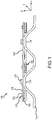
- FIG. 1 a system 100 for transferring heat from printed circuit boards (PCBs) is shown.
- An X-Y-Z axis is shown throughout the drawings to illustrate respective orientations of components.
- the system 100 may be included on an aircraft, such as in a passenger compartment.
- the system 100 includes multiple PCBs including a first PCB 102 and a second PCB 104.
- the PCB 102 includes a first side 106 and a second side 108.
- Various electrical and other components may be coupled to the PCB 102.
- the PCB 102 may include a light emitting diode (LED) 110 located on the first side 106, various electrical components 107 located on the first side 106, and various electrical components 112 located on the second side 108.
- the various electrical components may include any one or more of resistors, capacitors, inductors, microchips, controllers, or the like.
- the system 100 may further include a corrugated heat sink 114.
- the corrugated heat sink 114 may include a thermally conductive material, such as metal.
- the corrugated heat sink 114 may include a plurality of ribs including a first rib 116 and a second rib 118.
- the first rib 116 may contact the first PCB 102, and the second rib 118 may contact the second PCB 104.
- the ribs 116, 118 may extend along a portion or all of the PCBs 102, 104 along the Y direction.
- Heat (i.e., thermal energy) from the PCB 102 may be transferred to the corrugated heat sink 114 via the first rib 116, and may be distributed into the environment by the corrugated heat sink 114.
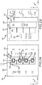
- FIG. 2A illustrates the first side 106 of the PCB 102 and FIG. 2B illustrates the second side 108 of the PCB 102.
- the first side 106 may include multiple LEDs coupled thereto.
- the multiple LEDs may include the LED 110, a second LED 226, a third LED 228, and a fourth LED 230.
- the PCB 102 may include any quantity of LEDs oriented in any fashion.
- the second side 108 of the PCB 102 may include a first metal strip 202.
- the first metal strip 202 may be elongated and may extend along the Y direction.
- the first rib 116 may contact the first metal strip 202 and may receive and distribute heat from the first metal strip 202.
- thermal paste, thermal tape, thermal pads, or other thermal materials may be located between the first rib 116 and the first metal strip 202 in order to facilitate the transfer of heat.
- the system 100 may still function as desired without such thermal materials.
- the first side 106 of the PCB 102 may include metal pads including a first metal pad 204 and a second metal pad 206.
- metal may refer to any conductive metallic or non-metallic conductive material.
- the LED 110 may include a first terminal 208 and a second terminal 210.
- the first terminal 208 or the second terminal 210 may be electrically connected to the anode of the LED 110 and the other of the first terminal 208 or the second terminal 210 may be electrically connected to the cathode of the LED 110.
- the first metal pad 204 may be electrically connected to the first terminal 208, and the second metal pad 206 may be electrically connected to the second terminal 210.
- the first metal pad 204 may be electrically isolated from the second metal pad 206.
- the first metal pad 204 and the second metal pad 206 may receive heat from the LED 110.
- the second side 108 of the PCB 102 may include second metal strips which may be split into a first portion 214 and a second portion 216.
- the first portion 214 and the second portion 216 may be electrically isolated from the first metal strip 202. Even with the electrical isolation, heat from the first portion 214 and the second portion 216 may be transferred to the first metal strip 202, from which it may be distributed to a heat sink (such as the heat sink 114).
- the first portion 214 may be electrically connected to the first metal pad 204.
- vias 218 may extend through the PCB 102 and may electrically connect the first portion 214 to the first metal pad 204.
- the vias 218 may be filled with a conductor, such as copper.
- the second portion 216 may be electrically connected to the second metal pad 206.
- vias 220 may extend through the PCB 102 and may electrically connect the second portion 216 to the second metal pad 206.
- the vias 220 may be filled with a conductor, such as copper.
- a portion of the heat may transfer through the PCB 102 and be received by the first metal strip 202.
- a portion of the heat may likewise transfer from the LED 110 to the first metal pad 204 and the second metal pad 206 by the proximity to the LED 110, and by the electrical connection between the pads 204, 206 and the terminals 208, 210.
- the heat received by the metal pads 204, 206 may be transferred to the first portion 214 and the second portion 216 by the vias 218, 220.
- the heat may then transfer from the first portion 214 and the second portion 216 to the first metal strip 202, where it may be received and distributed by a heat sink.
- An aperture 222 (e.g., a countersink) may be formed through the PCB 102.
- the aperture 222 may be formed in the center of the X-Y plane of the PCB.
- a fastener 224 may extend through the aperture 222 and may fasten the PCB 102 to the corrugated heat sink 114.
- the PCB 102 includes the LEDs 110, 226, 228, 230.
- multiple first metal pads 204 may be included on the PCB 102.
- one metal pad 204 may be used for each LED, one metal pad 204 may be used for two LEDs, one metal pad 204 may be used for the combination of all LEDs, or the like.
- multiple second metal pads 206 may be included on the PCB 102.
- one second metal pad 206 may be used for each LED, one second metal pad may be used for two LEDs, one second metal pad 206 may be used for the combination of all LEDs, or the like.
- the same may be true for the first portion 214 and the second portion 216 of the second metal strips 212. That is, the PCB 102 may include one or multiple first portions 214 and one or multiple second portions 216.
- the system 100 may be implemented in or on an exterior of an aircraft to provide exterior lighting to the aircraft.
- the PCB 102 may be installed on an exterior of a fuselage, wings, landing gear, blades, or the like of an aircraft.
- the PCB 102 is designed to be coupled to a portion of an aircraft such as an exterior portion (e.g., a portion in contact with the environment of the aircraft).
- the ability to place the electrical components 112 on the second side 208 of the PCB 102 allows for denser placement of components on the PCB 102. This desirably results in the entire system 100 being smaller than if components are only able to be placed on the first side 106.
- the corrugated heat sink 114 of FIG. 1 has a variable distance to the PCB 102 (e.g., the first rib 116 contacts the PCB 102 while the area between the first rib 116 and the second rib 118 fails to contact the PCB 102). This variable distance allows the placement of the electrical components 112 on the second side 108 (e.g., the electrical components 112 are located in an area with a greater distance between the corrugated heat sink 114 and the PCB 102).
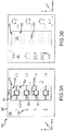
- the system 300 includes a PCB 302 having a first side 304 and a second side 306.
- a plurality of LEDs 324 including a first LED 301 are located on the first side 304.
- a plurality of electrical components 308 may be located on the first side 304, and a plurality of electrical components 310 may be located on the second side 306.
- a metal strip 312 may be positioned on the second side 306.
- a plurality of metal pads 314 including a first metal pad 316 may be positioned on the first side 304.
- the metal pads 314 may be electrically isolated from the LEDs 324 and may include any quantity of metal pads.
- the metal pads 314 may include a single metal pad that includes cutouts or openings for the LEDs 324.
- the metal pads 314 may include separate metal pads surrounding each of the LEDs 324.
- the metal pads 314 may include a single metal pad between each LED 324 and on the outer ends of the outer LEDs 324 (i.e., the first metal pad 316 on the outer end of the outer LED 301, and a second metal pad 318 between the LED 301 and an adjacent LED 303).
- the metal pads 314 may be shaped to partially or fully surround the LEDs 324 along the X-Y plane.
- the metal pads 314 may be electrically connected to the metal strip 312.
- a first plurality of vias 320 may electrically connect the first metal pad 316 to the metal strip 312, and a second plurality of vias 322 may electrically connect the second metal pad 318 to the metal strip 312.
- the vias 320, 322 may be filled with a conductor, such as copper.
- An aperture 326 may be formed through the PCB 302 and may be used in conjunction with a fastener to couple the PCB 302 to a heat sink (such as the corrugated heat sink 114 of FIG. 1 ).
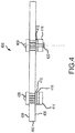
- the system 400 may be used in conjunction with the PCB 102 of FIGS. 2A and 2B , with the PCB 302 of FIGS. 3A and 3B , or with other PCBs.
- the system 400 may include a PCB 402 having a first side 404 and a second side 406.
- a first LED 408 and a second LED 409 may be located on the first side 404.
- a first metal strip 410 may be located on the second side 406 and designed to receive heat from the first LED 408, and a second metal strip 412 may also be located on the second side 406 and designed to receive heat from the second LED 409.
- the system 400 may include surface mounted heat sinks.
- a first conductive surface mounted heat sink 414 may be coupled to the second side 406 and in contact with the first metal strip 410
- a second conductive surface mounted heat sink 416 may be coupled to the second side 406 and in contact with the second metal strip 412.
- the conductive surface mounted heat sink 414, 416 may be coupled to the PCB 402 in any known manner.
- the first conductive surface mounted heat sink 414 may be coupled to the first metal strip 410 using a thermal adhesive (e.g., a two-part epoxy resin or cyanoacrylate).
- the second conductive surface mounted heat sink 416 may be coupled to the second metal strip 412 using a fastener 420.
- references to "various embodiments”, “one embodiment”, “an embodiment”, “an example embodiment”, etc. indicate that the embodiment described may include a particular feature, structure, or characteristic, but every embodiment may not necessarily include the particular feature, structure, or characteristic. Moreover, such phrases are not necessarily referring to the same embodiment. Further, when a particular feature, structure, or characteristic is described in connection with an embodiment, it is submitted that it is within the knowledge of one skilled in the art to affect such feature, structure, or characteristic in connection with other embodiments whether or not explicitly described. After reading the description, it will be apparent to one skilled in the relevant art(s) how to implement the disclosure in alternative embodiments.
Landscapes
- Engineering & Computer Science (AREA)
- Microelectronics & Electronic Packaging (AREA)
- General Engineering & Computer Science (AREA)
- Physics & Mathematics (AREA)
- Optics & Photonics (AREA)
- Aviation & Aerospace Engineering (AREA)
- Manufacturing & Machinery (AREA)
- Cooling Or The Like Of Semiconductors Or Solid State Devices (AREA)
- Led Device Packages (AREA)
- Arrangement Of Elements, Cooling, Sealing, Or The Like Of Lighting Devices (AREA)
Abstract
Description
- The present disclosure relates to systems for distributing heat from a printed circuit board having one or more light emitting diode.
- Prolonged exposure to heat may cause certain electrical components (e.g., high power light emitting diodes (LEDs)) to degrade over time. Also, LEDs may generate more heat than other electrical components. A conventional approach to distributing heat from printed circuit boards (PCBs) that include LEDs has been to directly connect the LEDs to a conventional heat sink. However, significant heat may remain on the PCB, especially if the LEDs are high power devices. Additionally, difficulty arises if electrical components are coupled to a different surface of the PCB than the surface to which the LEDs are mounted.
- Disclosed herein is a system for transferring heat from printed circuit boards (PCBs) with light emitting diodes (LEDs). The system includes a PCB having a first side and a second side and configured to be coupled to an exterior portion of an aircraft. The system further includes a LED located on the first side of the PCB. The system further includes a first metal strip located on the second side of the PCB. The system further includes a heat sink configured to contact the first metal strip to dissipate heat from the PCB.
- Any of the foregoing embodiments may further include a metal pad located on the first side of the PCB; and a second metal strip located on the second side of the PCB and electrically connected to the metal pad located on the first side of the PCB.
- In any of the foregoing embodiments, the second metal strip is electrically connected to the metal pad via metal-filled vias, and the second metal strip is electrically isolated from the first metal strip.
- In any of the foregoing embodiments, the LED has a first terminal and a second terminal; the metal pad includes a first metal pad electrically connected to the first terminal of the LED and a second metal pad electrically connected to the second terminal of the LED; and the second metal strip includes a first portion electrically connected to the first metal pad and a second portion electrically connected to the second metal pad.
- Any of the foregoing embodiments may further include a metal pad located on the first side of the PCB, electrically isolated from the LED, and electrically connected to the first metal strip.
- Any of the foregoing embodiments may further include an aperture extending through the PCB and the first metal strip and configured to receive a fastener to couple the PCB to the heat sink.
- In any of the foregoing embodiments, the heat sink includes a corrugated heat sink separate from the PCB and having a first rib configured to contact and extend along the first metal strip to dissipate heat from the PCB.
- In any of the foregoing embodiments, the heat sink includes a conductive surface mounted component configured to be mounted to the PCB.
- Any of the foregoing embodiments may further include electrical components coupled to the second side of the PCB.
- Also disclosed is a system for transferring heat from printed circuit boards (PCBs) with light emitting diodes (LEDs). The system includes a PCB having a first side and a second side and configured to be coupled to an exterior portion of an aircraft. The system further includes a LED located on the first side of the PCB. The system further includes a first metal strip located on the second side of the PCB. The system further includes a corrugated heat sink separate from the PCB and having a first rib configured to contact and extend along the first metal strip to dissipate heat from the PCB.
- Any of the foregoing embodiments may further include a metal pad located on the first side of the PCB; and a second metal strip located on the second side of the PCB and electrically connected to the metal pad located on the first side of the PCB.
- In any of the foregoing embodiments, the second metal strip is electrically connected to the metal pad via metal-filled vias, and the second metal strip is electrically isolated from the first metal strip.
- In any of the foregoing embodiments, the LED has a first terminal and a second terminal; the metal pad includes a first metal pad electrically connected to the first terminal of the LED and a second metal pad electrically connected to the second terminal of the LED; and the second metal strip includes a first portion electrically connected to the first metal pad and a second portion electrically connected to the second metal pad.
- Any of the foregoing embodiments may further include a metal pad located on the first side of the PCB, electrically isolated from the LED, and electrically connected to the first metal strip.
- Any of the foregoing embodiments may further include an aperture extending through the PCB and the first metal strip and configured to receive a fastener to couple the PCB to the corrugated heat sink.
- Also disclosed is a system for transferring heat from printed circuit boards (PCBs) with light emitting diodes (LEDs). The system includes a PCB having a first side and a second side and configured to be coupled to an exterior portion of an aircraft. The system further includes a LED located on the first side of the PCB. The system further includes a first metal strip located on the second side of the PCB. The system further includes a conductive surface mounted component configured to be mounted to the second side of the PCB, to be in contact with the first metal strip, and to dissipate heat from the PCB.
- Any of the foregoing embodiments may further include a metal pad located on the first side of the PCB; and a second metal strip located on the second side of the PCB and electrically connected to the metal pad located on the first side of the PCB.
- In any of the foregoing embodiments, the second metal strip is electrically connected to the metal pad via metal-filled vias, and the second metal strip is electrically isolated from the first metal strip.
- In any of the foregoing embodiments, the LED has a first terminal and a second terminal; the metal pad includes a first metal pad electrically connected to the first terminal of the LED and a second metal pad electrically connected to the second terminal of the LED; and the second metal strip includes a first portion electrically connected to the first metal pad and a second portion electrically connected to the second metal pad.
- Any of the foregoing embodiments may further include a metal pad located on the first side of the PCB, electrically isolated from the LED, and electrically connected to the first metal strip.
- The foregoing features and elements may be combined in various combinations without exclusivity, unless expressly indicated otherwise. These features and elements as well as the operation thereof will become more apparent in light of the following description and the accompanying drawings. It should be understood, however, the following description and drawings are intended to be exemplary in nature and non-limiting.
- The subject matter of the present disclosure is particularly pointed out and distinctly claimed in the concluding portion of the specification. A more complete understanding of the present disclosure, however, may best be obtained by referring to the detailed description and claims when considered in connection with the figures, wherein like numerals denote like elements.
-
FIG. 1 illustrates a system for distributing heat from a printed circuit board (PCB) having a light emitting diode (LED), the system utilizing a corrugated heat sink, in accordance with various embodiments; -
FIGS. 2A and 2B illustrate a first side and a second side, respectively, of a PCB of the system ofFIG. 1 , in accordance with various embodiments; -
FIGS. 3A and 3B illustrate a first side and a second side, respectively, of a PCB of a system for distributing heat from a PCB having a LED, in accordance with various embodiments; and -
FIG. 4 illustrates a system for distributing heat from a PCB having a LED, the system utilizing conductive surface mounted components as heat sinks, in accordance with various embodiments. - The detailed description of exemplary embodiments herein makes reference to the accompanying drawings, which show exemplary embodiments by way of illustration. While these exemplary embodiments are described in sufficient detail to enable those skilled in the art to practice the exemplary embodiments of the disclosure, it should be understood that other embodiments may be realized and that logical changes and adaptations in design and construction may be made in accordance with this disclosure and the teachings herein. Thus, the detailed description herein is presented for purposes of illustration only and not limitation. The steps recited in any of the method or process descriptions may be executed in any order and are not necessarily limited to the order presented.
- Furthermore, any reference to singular includes plural embodiments, and any reference to more than one component or step may include a singular embodiment or step. Also, any reference to attached, fixed, connected or the like may include permanent, removable, temporary, partial, full and/or any other possible attachment option. Additionally, any reference to without contact (or similar phrases) may also include reduced contact or minimal contact. Surface shading lines may be used throughout the figures to denote different parts but not necessarily to denote the same or different materials.
- Referring now to
FIG. 1 , asystem 100 for transferring heat from printed circuit boards (PCBs) is shown. An X-Y-Z axis is shown throughout the drawings to illustrate respective orientations of components. In various embodiments, thesystem 100 may be included on an aircraft, such as in a passenger compartment. - The
system 100 includes multiple PCBs including afirst PCB 102 and asecond PCB 104. ThePCB 102 includes afirst side 106 and asecond side 108. Various electrical and other components may be coupled to thePCB 102. In particular, thePCB 102 may include a light emitting diode (LED) 110 located on thefirst side 106, variouselectrical components 107 located on thefirst side 106, and variouselectrical components 112 located on thesecond side 108. The various electrical components may include any one or more of resistors, capacitors, inductors, microchips, controllers, or the like. - The
system 100 may further include acorrugated heat sink 114. Thecorrugated heat sink 114 may include a thermally conductive material, such as metal. Thecorrugated heat sink 114 may include a plurality of ribs including afirst rib 116 and asecond rib 118. Thefirst rib 116 may contact thefirst PCB 102, and thesecond rib 118 may contact thesecond PCB 104. Theribs PCBs PCB 102 may be transferred to thecorrugated heat sink 114 via thefirst rib 116, and may be distributed into the environment by thecorrugated heat sink 114. - Referring now to
FIGS. 2A and 2B , additional details of thesystem 100 are shown.FIG. 2A illustrates thefirst side 106 of thePCB 102 andFIG. 2B illustrates thesecond side 108 of thePCB 102. In particular, thefirst side 106 may include multiple LEDs coupled thereto. The multiple LEDs may include theLED 110, asecond LED 226, athird LED 228, and afourth LED 230. In various embodiments, thePCB 102 may include any quantity of LEDs oriented in any fashion. - The
second side 108 of thePCB 102 may include afirst metal strip 202. Thefirst metal strip 202 may be elongated and may extend along the Y direction. With brief reference toFIGS. 1 and2B , thefirst rib 116 may contact thefirst metal strip 202 and may receive and distribute heat from thefirst metal strip 202. In various embodiments, thermal paste, thermal tape, thermal pads, or other thermal materials may be located between thefirst rib 116 and thefirst metal strip 202 in order to facilitate the transfer of heat. However, thesystem 100 may still function as desired without such thermal materials. - Returning reference to
FIGS. 2A and 2B , thefirst side 106 of thePCB 102 may include metal pads including afirst metal pad 204 and asecond metal pad 206. Where used in this context, "metal" may refer to any conductive metallic or non-metallic conductive material. TheLED 110 may include afirst terminal 208 and asecond terminal 210. In various embodiments, thefirst terminal 208 or thesecond terminal 210 may be electrically connected to the anode of theLED 110 and the other of thefirst terminal 208 or thesecond terminal 210 may be electrically connected to the cathode of theLED 110. Thefirst metal pad 204 may be electrically connected to thefirst terminal 208, and thesecond metal pad 206 may be electrically connected to thesecond terminal 210. In that regard, thefirst metal pad 204 may be electrically isolated from thesecond metal pad 206. Thefirst metal pad 204 and thesecond metal pad 206 may receive heat from theLED 110. - The
second side 108 of thePCB 102 may include second metal strips which may be split into afirst portion 214 and asecond portion 216. Thefirst portion 214 and thesecond portion 216 may be electrically isolated from thefirst metal strip 202. Even with the electrical isolation, heat from thefirst portion 214 and thesecond portion 216 may be transferred to thefirst metal strip 202, from which it may be distributed to a heat sink (such as the heat sink 114). - The
first portion 214 may be electrically connected to thefirst metal pad 204. For example, vias 218 may extend through thePCB 102 and may electrically connect thefirst portion 214 to thefirst metal pad 204. In various embodiments, thevias 218 may be filled with a conductor, such as copper. Thesecond portion 216 may be electrically connected to thesecond metal pad 206. For example, vias 220 may extend through thePCB 102 and may electrically connect thesecond portion 216 to thesecond metal pad 206. In various embodiments, thevias 220 may be filled with a conductor, such as copper. - As heat is generated by the LED 110 (as well as the
electrical components 107, 112), a portion of the heat may transfer through thePCB 102 and be received by thefirst metal strip 202. A portion of the heat may likewise transfer from theLED 110 to thefirst metal pad 204 and thesecond metal pad 206 by the proximity to theLED 110, and by the electrical connection between thepads terminals metal pads first portion 214 and thesecond portion 216 by thevias first portion 214 and thesecond portion 216 to thefirst metal strip 202, where it may be received and distributed by a heat sink. - An aperture 222 (e.g., a countersink) may be formed through the
PCB 102. In various embodiments, theaperture 222 may be formed in the center of the X-Y plane of the PCB. With brief reference toFIGS. 1 ,2A, and 2B , afastener 224 may extend through theaperture 222 and may fasten thePCB 102 to thecorrugated heat sink 114. - As shown, the
PCB 102 includes theLEDs first metal pads 204 may be included on thePCB 102. In various embodiments, onemetal pad 204 may be used for each LED, onemetal pad 204 may be used for two LEDs, onemetal pad 204 may be used for the combination of all LEDs, or the like. Likewise, multiplesecond metal pads 206 may be included on thePCB 102. In various embodiments, onesecond metal pad 206 may be used for each LED, one second metal pad may be used for two LEDs, onesecond metal pad 206 may be used for the combination of all LEDs, or the like. The same may be true for thefirst portion 214 and thesecond portion 216 of the second metal strips 212. That is, thePCB 102 may include one or multiplefirst portions 214 and one or multiplesecond portions 216. - The
system 100 may be implemented in or on an exterior of an aircraft to provide exterior lighting to the aircraft. For example, thePCB 102 may be installed on an exterior of a fuselage, wings, landing gear, blades, or the like of an aircraft. In that regard, thePCB 102 is designed to be coupled to a portion of an aircraft such as an exterior portion (e.g., a portion in contact with the environment of the aircraft). - The ability to place the
electrical components 112 on thesecond side 208 of thePCB 102 allows for denser placement of components on thePCB 102. This desirably results in theentire system 100 being smaller than if components are only able to be placed on thefirst side 106. Thecorrugated heat sink 114 ofFIG. 1 has a variable distance to the PCB 102 (e.g., thefirst rib 116 contacts thePCB 102 while the area between thefirst rib 116 and thesecond rib 118 fails to contact the PCB 102). This variable distance allows the placement of theelectrical components 112 on the second side 108 (e.g., theelectrical components 112 are located in an area with a greater distance between thecorrugated heat sink 114 and the PCB 102). - Turning now to
FIGS. 3A and 3B , anothersystem 300 for transferring heat from PCBs with LEDs is shown. Thesystem 300 includes aPCB 302 having afirst side 304 and asecond side 306. A plurality ofLEDs 324 including afirst LED 301 are located on thefirst side 304. A plurality ofelectrical components 308 may be located on thefirst side 304, and a plurality ofelectrical components 310 may be located on thesecond side 306. - A
metal strip 312 may be positioned on thesecond side 306. A plurality ofmetal pads 314 including afirst metal pad 316 may be positioned on thefirst side 304. Themetal pads 314 may be electrically isolated from theLEDs 324 and may include any quantity of metal pads. For example, themetal pads 314 may include a single metal pad that includes cutouts or openings for theLEDs 324. As another example, themetal pads 314 may include separate metal pads surrounding each of theLEDs 324. As another example, themetal pads 314 may include a single metal pad between eachLED 324 and on the outer ends of the outer LEDs 324 (i.e., thefirst metal pad 316 on the outer end of theouter LED 301, and a second metal pad 318 between theLED 301 and an adjacent LED 303). Themetal pads 314 may be shaped to partially or fully surround theLEDs 324 along the X-Y plane. - The
metal pads 314 may be electrically connected to themetal strip 312. For example, a first plurality ofvias 320 may electrically connect thefirst metal pad 316 to themetal strip 312, and a second plurality ofvias 322 may electrically connect the second metal pad 318 to themetal strip 312. In various embodiments, thevias - An
aperture 326 may be formed through thePCB 302 and may be used in conjunction with a fastener to couple thePCB 302 to a heat sink (such as thecorrugated heat sink 114 ofFIG. 1 ). - Turning now to
FIG. 4 , anothersystem 400 for transferring heat from PCBs is shown. Thesystem 400 may be used in conjunction with thePCB 102 ofFIGS. 2A and 2B , with thePCB 302 ofFIGS. 3A and 3B , or with other PCBs. Thesystem 400 may include aPCB 402 having afirst side 404 and asecond side 406. Afirst LED 408 and asecond LED 409 may be located on thefirst side 404. Afirst metal strip 410 may be located on thesecond side 406 and designed to receive heat from thefirst LED 408, and asecond metal strip 412 may also be located on thesecond side 406 and designed to receive heat from thesecond LED 409. - Rather than using a corrugated heat sink, the
system 400 may include surface mounted heat sinks. In particular, a first conductive surface mountedheat sink 414 may be coupled to thesecond side 406 and in contact with thefirst metal strip 410, and a second conductive surface mounted heat sink 416 may be coupled to thesecond side 406 and in contact with thesecond metal strip 412. The conductive surface mountedheat sink 414, 416 may be coupled to thePCB 402 in any known manner. For example, the first conductive surface mountedheat sink 414 may be coupled to thefirst metal strip 410 using a thermal adhesive (e.g., a two-part epoxy resin or cyanoacrylate). As another example, the second conductive surface mounted heat sink 416 may be coupled to thesecond metal strip 412 using afastener 420. - Benefits and other advantages have been described herein with regard to specific embodiments. Furthermore, the connecting lines shown in the various figures contained herein are intended to represent exemplary functional relationships and/or physical couplings between the various elements. It should be noted that many alternative or additional functional relationships or physical connections may be present in a practical system. However, the benefits, advantages, and any elements that may cause any benefit or advantage to occur or become more pronounced are not to be construed as critical, required, or essential features or elements of the disclosure. The scope of the disclosure is accordingly to be limited by nothing other than the appended claims, in which reference to an element in the singular is not intended to mean "one and only one" unless explicitly so stated, but rather "one or more." Moreover, where a phrase similar to "at least one of A, B, or C" is used in the claims, it is intended that the phrase be interpreted to mean that A alone may be present in an embodiment, B alone may be present in an embodiment, C alone may be present in an embodiment, or that any combination of the elements A, B and C may be present in a single embodiment; for example, A and B, A and C, B and C, or A and B and C.
- Systems, methods and apparatus are provided herein. In the detailed description herein, references to "various embodiments", "one embodiment", "an embodiment", "an example embodiment", etc., indicate that the embodiment described may include a particular feature, structure, or characteristic, but every embodiment may not necessarily include the particular feature, structure, or characteristic. Moreover, such phrases are not necessarily referring to the same embodiment. Further, when a particular feature, structure, or characteristic is described in connection with an embodiment, it is submitted that it is within the knowledge of one skilled in the art to affect such feature, structure, or characteristic in connection with other embodiments whether or not explicitly described. After reading the description, it will be apparent to one skilled in the relevant art(s) how to implement the disclosure in alternative embodiments.
Claims (9)
- A system for transferring heat from printed circuit boards, PCBs, with light emitting diodes, LEDs, the system comprising:a PCB (102) having a first side (106) and a second side (108) and configured to be coupled to an exterior portion of an aircraft;a LED (110) located on the first side of the PCB;a first metal strip (202) located on the second side of the PCB; anda heat sink (114) configured to contact the first metal strip to dissipate heat from the PCB.
- The system of claim 1, further comprising:a metal pad (204, 206) located on the first side of the PCB; anda second metal strip located on the second side of the PCB and electrically connected to the metal pad located on the first side of the PCB.
- The system of claim 2, wherein the second metal strip is electrically connected to the metal pad via metal-filled vias, and the second metal strip is electrically isolated from the first metal strip.
- The system of claim 2 or 3, wherein:the LED has a first terminal (208) and a second terminal (210);the metal pad includes a first metal pad (204) electrically connected to the first terminal of the LED and a second metal pad (206) electrically connected to the second terminal of the LED; andthe second metal strip includes a first portion electrically connected to the first metal pad and a second portion electrically connected to the second metal pad.
- The system of any preceding claim, further comprising a metal pad located on the first side of the PCB, electrically isolated from the LED, and electrically connected to the first metal strip.
- The system of any preceding claim, further comprising an aperture extending through the PCB and the first metal strip and configured to receive a fastener to couple the PCB to the heat sink.
- The system any preceding claim, wherein the heat sink includes a corrugated heat sink (114) separate from the PCB and having a first rib (116) configured to contact and extend along the first metal strip to dissipate heat from the PCB.
- The system of any of claims 1 to 6, wherein the heat sink includes a conductive surface mounted component (414, 416) configured to be mounted to the PCB.
- The system of any preceding claim, further comprising electrical components coupled to the second side of the PCB.
Applications Claiming Priority (1)
| Application Number | Priority Date | Filing Date | Title |
|---|---|---|---|
| US16/685,813 US10986722B1 (en) | 2019-11-15 | 2019-11-15 | High performance heat sink for double sided printed circuit boards |
Publications (1)
| Publication Number | Publication Date |
|---|---|
| EP3823423A1 true EP3823423A1 (en) | 2021-05-19 |
Family
ID=73452131
Family Applications (1)
| Application Number | Title | Priority Date | Filing Date |
|---|---|---|---|
| EP20207889.5A Pending EP3823423A1 (en) | 2019-11-15 | 2020-11-16 | System for transferring heat from printed circuit boards with light emitting diodes |
Country Status (2)
| Country | Link |
|---|---|
| US (1) | US10986722B1 (en) |
| EP (1) | EP3823423A1 (en) |
Citations (7)
| Publication number | Priority date | Publication date | Assignee | Title |
|---|---|---|---|---|
| US20080099770A1 (en) * | 2006-10-31 | 2008-05-01 | Medendorp Nicholas W | Integrated heat spreaders for light emitting devices (LEDs) and related assemblies |
| US20080291631A1 (en) * | 2007-05-23 | 2008-11-27 | Leopold Hellinger | Illumination unit |
| WO2009028812A2 (en) * | 2007-08-28 | 2009-03-05 | Lg Innotek Co., Ltd | Light emitting device |
| EP2642532A1 (en) * | 2011-11-09 | 2013-09-25 | Dongguan Kingsun Optoelectronic Co., Ltd | Process for manufacturing heat sink structure for high-power led |
| US20130314920A1 (en) * | 2012-05-25 | 2013-11-28 | Myung Ho Park | Direct Heat Sink Technology for LEDs and Driving Circuits |
| US20160324031A1 (en) * | 2013-11-12 | 2016-11-03 | Jnc Corporation | Heat sink |
| US20180340682A1 (en) * | 2017-05-24 | 2018-11-29 | Osram Sylvania Inc. | Lighting device modules |
Family Cites Families (25)
| Publication number | Priority date | Publication date | Assignee | Title |
|---|---|---|---|---|
| GB0106547D0 (en) * | 2001-03-16 | 2001-05-02 | Aavid Thermalloy Ltd | Heat sinks |
| US7775685B2 (en) * | 2003-05-27 | 2010-08-17 | Cree, Inc. | Power surface mount light emitting die package |
| TWI333576B (en) * | 2005-08-17 | 2010-11-21 | Au Optronics Corp | Bottom lighting module |
| EP2018796A1 (en) * | 2006-05-08 | 2009-01-28 | Koninklijke Philips Electronics N.V. | Thermal surface mounting of multiple leds onto a heatsink |
| US20110278638A1 (en) * | 2008-03-25 | 2011-11-17 | Lin Charles W C | Semiconductor chip assembly with post/dielectric/post heat spreader |
| CN101645478A (en) * | 2008-08-08 | 2010-02-10 | 鸿富锦精密工业(深圳)有限公司 | Light emitting diode (LED) radiating structure |
| CN101650010A (en) * | 2008-08-14 | 2010-02-17 | 鸿富锦精密工业(深圳)有限公司 | LED light source module and light machine applied by same |
| WO2010110572A2 (en) * | 2009-03-24 | 2010-09-30 | Kim Kang | Light-emitting diode package |
| US8152337B2 (en) | 2009-05-01 | 2012-04-10 | Billboard Video, Inc. | Electronic display panel |
| WO2011111399A1 (en) * | 2010-03-11 | 2011-09-15 | パナソニック株式会社 | Light emitting module, light source device, liquid crystal display device, and method for manufacturing light emitting module |
| KR101735571B1 (en) * | 2010-08-20 | 2017-05-16 | 삼성전자주식회사 | Thermal dissipation material and light emitting diode package including a junction part made of the thermal dissipation material |
| US8354684B2 (en) * | 2011-01-09 | 2013-01-15 | Bridgelux, Inc. | Packaging photon building blocks having only top side connections in an interconnect structure |
| US8737073B2 (en) * | 2011-02-09 | 2014-05-27 | Tsmc Solid State Lighting Ltd. | Systems and methods providing thermal spreading for an LED module |
| US8632221B2 (en) * | 2011-11-01 | 2014-01-21 | Taiwan Semiconductor Manufacturing Company, Ltd. | LED module and method of bonding thereof |
| JP2015505172A (en) * | 2012-01-25 | 2015-02-16 | コーニンクレッカ フィリップス エヌ ヴェ | LED module, LED unit, and luminaire including LED module |
| US8783911B2 (en) * | 2012-02-17 | 2014-07-22 | Tsmc Solid State Lighting Ltd. | LED packaging structure having improved thermal dissipation and mechanical strength |
| US9195281B2 (en) | 2013-12-31 | 2015-11-24 | Ultravision Technologies, Llc | System and method for a modular multi-panel display |
| US20170263546A1 (en) * | 2014-03-07 | 2017-09-14 | Bridge Semiconductor Corporation | Wiring board with electrical isolator and base board incorporated therein and semiconductor assembly and manufacturing method thereof |
| US20150260390A1 (en) * | 2014-03-14 | 2015-09-17 | Eric Colin Bretschneider | Composite Heat Sink For Electrical Components |
| US20160064630A1 (en) * | 2014-08-26 | 2016-03-03 | Texas Instruments Incorporated | Flip chip led package |
| CN106605310B (en) * | 2014-09-01 | 2019-11-01 | 株式会社钟化 | LED lamp for car radiator |
| ES2883643T3 (en) * | 2015-10-01 | 2021-12-09 | Emergency Tech Inc | Lighting element for a vehicle |
| KR102365686B1 (en) | 2016-03-16 | 2022-02-21 | 삼성전자주식회사 | Light Emitting Diode(LED) Driving Apparatus and Lighting Device |
| JP6677816B2 (en) * | 2016-10-25 | 2020-04-08 | 京セラ株式会社 | Light emitting element mounting substrate, light emitting device and light emitting module |
| US10561045B2 (en) | 2018-03-19 | 2020-02-11 | Dolby Laboratories Licensing Corporation | Surface mount heatsink attachment |
-
2019
- 2019-11-15 US US16/685,813 patent/US10986722B1/en active Active
-
2020
- 2020-11-16 EP EP20207889.5A patent/EP3823423A1/en active Pending
Patent Citations (7)
| Publication number | Priority date | Publication date | Assignee | Title |
|---|---|---|---|---|
| US20080099770A1 (en) * | 2006-10-31 | 2008-05-01 | Medendorp Nicholas W | Integrated heat spreaders for light emitting devices (LEDs) and related assemblies |
| US20080291631A1 (en) * | 2007-05-23 | 2008-11-27 | Leopold Hellinger | Illumination unit |
| WO2009028812A2 (en) * | 2007-08-28 | 2009-03-05 | Lg Innotek Co., Ltd | Light emitting device |
| EP2642532A1 (en) * | 2011-11-09 | 2013-09-25 | Dongguan Kingsun Optoelectronic Co., Ltd | Process for manufacturing heat sink structure for high-power led |
| US20130314920A1 (en) * | 2012-05-25 | 2013-11-28 | Myung Ho Park | Direct Heat Sink Technology for LEDs and Driving Circuits |
| US20160324031A1 (en) * | 2013-11-12 | 2016-11-03 | Jnc Corporation | Heat sink |
| US20180340682A1 (en) * | 2017-05-24 | 2018-11-29 | Osram Sylvania Inc. | Lighting device modules |
Also Published As
| Publication number | Publication date |
|---|---|
| US10986722B1 (en) | 2021-04-20 |
Similar Documents
| Publication | Publication Date | Title |
|---|---|---|
| US10576912B2 (en) | Circuit assembly and electrical junction box | |
| CN110431664B (en) | Mounting LED elements on a flat carrier | |
| US7957156B2 (en) | Busbar circuit board assembly | |
| US8482929B2 (en) | Systems for circuit board heat transfer and method of assembling same | |
| US20070010086A1 (en) | Circuit board with a through hole wire and manufacturing method thereof | |
| EP3327767B1 (en) | Mount structure, method of manufacturing mount structure, and wireless device | |
| US20130170145A1 (en) | Thermal connector | |
| US9839128B2 (en) | Solder void reduction between electronic packages and printed circuit boards | |
| US20180370463A1 (en) | Circuit assembly and electrical junction box | |
| US7688591B2 (en) | Electronic-component-mounting board | |
| EP3345464B1 (en) | Method of making an led device | |
| US9693459B2 (en) | Circuit board assembly and method of manufacturing same | |
| US7265983B2 (en) | Power unit comprising a heat sink, and assembly method | |
| US10383209B2 (en) | Electronic assembly for lighting applications, lighting device and method for producing an electronic assembly | |
| US20150092373A1 (en) | Mounting solution for components on a very fine pitch array | |
| US10986722B1 (en) | High performance heat sink for double sided printed circuit boards | |
| US20170294428A1 (en) | Method of producing optoelectronic modules and an assembly having a module | |
| CN105493279B (en) | System for attaching devices to flexible substrates | |
| GB2480428A (en) | PCB with metal core having extended heatsink bosses for mounting LEDs | |
| CN213305838U (en) | High-thickness copper composite circuit board | |
| CN105848415B (en) | Circuit module with surface-mount pins on side, circuit board and system | |
| US9107296B2 (en) | Thermo/electrical conductor arrangement for multilayer printed circuit boards | |
| US9504157B2 (en) | Hybrid circuit assembly | |
| EP2200408A1 (en) | Circuit board device, in particular for an electric power consuming device in a motor vehicle | |
| US20250185169A1 (en) | Delivery of power to a chip through a daughter board using connective electrical components |
Legal Events
| Date | Code | Title | Description |
|---|---|---|---|
| PUAI | Public reference made under article 153(3) epc to a published international application that has entered the european phase |
Free format text: ORIGINAL CODE: 0009012 |
|
| STAA | Information on the status of an ep patent application or granted ep patent |
Free format text: STATUS: THE APPLICATION HAS BEEN PUBLISHED |
|
| AK | Designated contracting states |
Kind code of ref document: A1 Designated state(s): AL AT BE BG CH CY CZ DE DK EE ES FI FR GB GR HR HU IE IS IT LI LT LU LV MC MK MT NL NO PL PT RO RS SE SI SK SM TR |
|
| STAA | Information on the status of an ep patent application or granted ep patent |
Free format text: STATUS: REQUEST FOR EXAMINATION WAS MADE |
|
| 17P | Request for examination filed |
Effective date: 20211119 |
|
| RBV | Designated contracting states (corrected) |
Designated state(s): AL AT BE BG CH CY CZ DE DK EE ES FI FR GB GR HR HU IE IS IT LI LT LU LV MC MK MT NL NO PL PT RO RS SE SI SK SM TR |
|
| P01 | Opt-out of the competence of the unified patent court (upc) registered |
Effective date: 20230922 |
|
| STAA | Information on the status of an ep patent application or granted ep patent |
Free format text: STATUS: EXAMINATION IS IN PROGRESS |
|
| 17Q | First examination report despatched |
Effective date: 20250318 |