EP3823303B1 - Electronic device including heat dissipation structure - Google Patents
Electronic device including heat dissipation structure Download PDFInfo
- Publication number
- EP3823303B1 EP3823303B1 EP19848656.5A EP19848656A EP3823303B1 EP 3823303 B1 EP3823303 B1 EP 3823303B1 EP 19848656 A EP19848656 A EP 19848656A EP 3823303 B1 EP3823303 B1 EP 3823303B1
- Authority
- EP
- European Patent Office
- Prior art keywords
- heat
- electronic device
- heat transfer
- transfer member
- disposed
- Prior art date
- Legal status (The legal status is an assumption and is not a legal conclusion. Google has not performed a legal analysis and makes no representation as to the accuracy of the status listed.)
- Active
Links
Images



Classifications
-
- H—ELECTRICITY
- H05—ELECTRIC TECHNIQUES NOT OTHERWISE PROVIDED FOR
- H05K—PRINTED CIRCUITS; CASINGS OR CONSTRUCTIONAL DETAILS OF ELECTRIC APPARATUS; MANUFACTURE OF ASSEMBLAGES OF ELECTRICAL COMPONENTS
- H05K7/00—Constructional details common to different types of electric apparatus
- H05K7/20—Modifications to facilitate cooling, ventilating, or heating
- H05K7/2039—Modifications to facilitate cooling, ventilating, or heating characterised by the heat transfer by conduction from the heat generating element to a dissipating body
- H05K7/20436—Inner thermal coupling elements in heat dissipating housings, e.g. protrusions or depressions integrally formed in the housing
- H05K7/20445—Inner thermal coupling elements in heat dissipating housings, e.g. protrusions or depressions integrally formed in the housing the coupling element being an additional piece, e.g. thermal standoff
-
- H—ELECTRICITY
- H04—ELECTRIC COMMUNICATION TECHNIQUE
- H04R—LOUDSPEAKERS, MICROPHONES, GRAMOPHONE PICK-UPS OR LIKE ACOUSTIC ELECTROMECHANICAL TRANSDUCERS; ELECTRIC HEARING AIDS; PUBLIC ADDRESS SYSTEMS
- H04R1/00—Details of transducers, loudspeakers or microphones
- H04R1/02—Casings; Cabinets ; Supports therefor; Mountings therein
-
- H—ELECTRICITY
- H04—ELECTRIC COMMUNICATION TECHNIQUE
- H04R—LOUDSPEAKERS, MICROPHONES, GRAMOPHONE PICK-UPS OR LIKE ACOUSTIC ELECTROMECHANICAL TRANSDUCERS; ELECTRIC HEARING AIDS; PUBLIC ADDRESS SYSTEMS
- H04R1/00—Details of transducers, loudspeakers or microphones
- H04R1/02—Casings; Cabinets ; Supports therefor; Mountings therein
- H04R1/023—Screens for loudspeakers
-
- H—ELECTRICITY
- H04—ELECTRIC COMMUNICATION TECHNIQUE
- H04R—LOUDSPEAKERS, MICROPHONES, GRAMOPHONE PICK-UPS OR LIKE ACOUSTIC ELECTROMECHANICAL TRANSDUCERS; ELECTRIC HEARING AIDS; PUBLIC ADDRESS SYSTEMS
- H04R3/00—Circuits for transducers
-
- H—ELECTRICITY
- H04—ELECTRIC COMMUNICATION TECHNIQUE
- H04R—LOUDSPEAKERS, MICROPHONES, GRAMOPHONE PICK-UPS OR LIKE ACOUSTIC ELECTROMECHANICAL TRANSDUCERS; ELECTRIC HEARING AIDS; PUBLIC ADDRESS SYSTEMS
- H04R9/00—Transducers of moving-coil, moving-strip, or moving-wire type
- H04R9/02—Details
- H04R9/022—Cooling arrangements
-
- H—ELECTRICITY
- H04—ELECTRIC COMMUNICATION TECHNIQUE
- H04R—LOUDSPEAKERS, MICROPHONES, GRAMOPHONE PICK-UPS OR LIKE ACOUSTIC ELECTROMECHANICAL TRANSDUCERS; ELECTRIC HEARING AIDS; PUBLIC ADDRESS SYSTEMS
- H04R2201/00—Details of transducers, loudspeakers or microphones covered by H04R1/00 but not provided for in any of its subgroups
- H04R2201/02—Details casings, cabinets or mounting therein for transducers covered by H04R1/02 but not provided for in any of its subgroups
- H04R2201/028—Structural combinations of loudspeakers with built-in power amplifiers, e.g. in the same acoustic enclosure
Definitions
- Various embodiments of the disclosure relate to a heat dissipation structure of an electronic device.
- the conventional electronic device may have at least one heating element such as a printed circuit board included therein, with a structure in which heat generated from the printed circuit board stays in a closed space of an enclosure since a heat dissipation structure for dissipating the heat is not provided inside the enclosure.
- a heating element such as a printed circuit board included therein
- the conventional electronic device does not have additional heat dissipation structure for dissipating heat generated therein to the outside, which results in a problem in that heat dissipation efficiency deteriorates.
- Various embodiments of the disclosure has a heat dissipation duct and a heat dissipation structure for transferring heat generated therein to the outside of a housing, thereby providing an electronic device capable of efficiently dissipating internal heat to the outside.
- Various embodiments of the disclosure uses a low-pitch or high-pitch amplifying device to pump internal heat to the outside, thereby providing an electronic device capable of effectively dissipating the heat.
- the present invention is directed to an electronic device as defined in claim 1.
- heat generated from a heating element inside an electronic device can be efficiently dissipated to the outside of acoustic holes through a heat transfer path consisting of a heat dissipation structure and a heat dissipation duct.
- FIG. 1 is a perspective view illustrating an exterior of an electronic device according to various embodiments of the disclosure.
- an electronic device 1000 may include a desk-type speaker which can be mounted on a desk, as a speaker capable of radiating a high-pitch or low-pitch sound.
- the electronic device 1000 may be an Artificial Intelligence (AI) speaker having a built-in microphone device.
- AI Artificial Intelligence
- the electronic device 1000 may include a housing 100 which constitutes an exterior and protects internal electronic components.
- the housing 100 may include an upper housing 11 and a lower housing 12.
- the housing 100 may include a plurality of leg portions 13 for mounting the device on a desk.
- the upper housing 11 may have a plurality of acoustic holes 110 constructed on an outer face.
- each of the acoustic holes 110 may be constructed generally on the upper housing 11, and may be constructed equi-distantly.
- the acoustic holes 110 may be holes for transferring a sound radiated from a sound generating device (not shown) to the outside.
- FIG. 2 is an exploded perspective view illustrating an enclosure disposed inside an electronic device according to various embodiments of the disclosure.
- a housing (e.g., the housing 100 of FIG. 1 ) of an electronic device (e.g., the electronic device 1000 of FIG. 1 ) according to various embodiments includes an enclosure 20.
- the enclosure 20 may be an internal housing capable of accommodating and supporting electronic components, for example, a printed circuit board, a power supply unit, or the like.
- the enclosure 20 may be surrounded by upper and lower housings 11 and 12 so as to be protected and supported.
- FIG. 3 is an exploded perspective view illustrating an inner structure of an enclosure according to various embodiments of the disclosure.
- an enclosure (e.g., the enclosure 20 of FIG. 2 ) according to various embodiments may include an upper enclosure 210 and a lower enclosure 212.
- the upper enclosure 210 may be coupled to the lower enclosure 212 by using at least one fastening structure.
- the enclosure 20 according to various embodiments includes etarte a power supply unit 22, a heat dissipation structure 28, and at least one printed circuit board 21.
- the enclosure 20 has the heat dissipation structure 28 accommodated in the upper enclosure 210.
- the heat dissipation structure 28 is a structure for transferring heat generated from the heating element 21 inside the enclosure 20 to the outside of acoustic holes 110.
- the heating element 21 includes a printed circuit board, on which a plurality of electronic components are mounted, the power supply unit 22, or the like.
- the printed circuit board may include an electronic component for amplifying an audio signal.
- the heat dissipation structure 28 is a structure coupled to the at least one heating element 21 to provide a heat transfer path for dissipating heat generated from the heating element 21 to the outside of the housing, and includes at least one heat transfer member, a heat dissipation duct (e.g., a heat dissipation duct 33 of FIG. 5 ), a Thermal Interfacing Material (TIM) 27, or the like.
- a heat dissipation duct e.g., a heat dissipation duct 33 of FIG. 5
- TIM Thermal Interfacing Material
- the heat dissipation structure 28 is a structure which provides a heat transfer path for dissipating heat generated from a heating element to outside portion, and may be a structure capable of transferring heat generated from a high-temperature heating element to the outside (e.g., a relatively low-temperature portion).
- the heat dissipation structure 28 includes first and second heat transfer members 25 and 26.
- the first heat transfer member 25 may be a member coupled to the printed circuit board 21 dedicated for amplification so that heat generated from the printed circuit board 21 dedicated for amplification is transferred to another heat transfer element.
- the first heat transfer member 25 may include a material (e.g., aluminum) of which a thermal conductive is higher than a designated range.
- the second heat transfer member 26 may be a heat transfer element coupled to the first heat transfer member 25 by means of the TIM so that heat generated from the first heat transfer member 25 is transferred to a heat dissipation duct.
- the TIM may be disposed between the first and second heat transfer members 25 and 26, so that heat is effectively transferred between them.
- the TIM 27 may be a member which serves to eliminate a gap caused by tolerances of processing and assembling components.
- the TIM 27 may include a silicone polymer material.
- the TIM 27 may serve to prevent a disjoint state, which may occur between the components when the electronic device 1000 operates.
- FIG. 4 is a cross-sectional view illustrating an inner structure of an electronic device according to various embodiments of the disclosure.
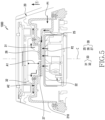
- FIG. 5 is a cross-sectional view illustrating a heat dissipation structure of an electronic device according to various embodiments of the disclosure.
- a heat dissipation structure 28 of an electronic device 1000 will be described with reference to FIG. 4 and FIG. 5 .
- an electronic device With respect to a power supply unit (e.g., the power supply unit 22 of FIG. 3 ) disposed coaxially with a central axis C, an electronic device according to various embodiments (e.g., the electronic device 1000 of FIG. 1 ) has a heat dissipation structure (e.g., the heat dissipation structure 28 of FIG. 3 ) disposed in a first direction of a power supply unit 22 and has a heat dissipation duct (e.g., the heat dissipation duct 33 of FIG. 5 ) located at an upper portion of the heat dissipation structure 28 to dissipation heat to the outside.
- a heat dissipation structure e.g., the heat dissipation structure 28 of FIG. 3
- a heat dissipation duct e.g., the heat dissipation duct 33 of FIG. 5
- the electronic device 1000 has at least one substrate (e.g., the printed circuit board 21 of FIG. 3 ) disposed in an outer circumferential direction of the power supply unit 22.
- a printed circuit board 21 mounted inside the enclosure 20 may include a printed circuit board for amplifying a sound, a printed circuit board related to an operation of the electronic device, a printed circuit board for operating the power supply unit, or the like.
- the printed circuit board dedicated for amplification may be disposed adjacent to the power supply unit 22, and may be disposed in an outer circumferential direction of the power supply unit 22.
- the printed circuit board 21 may be fastened to an enclosure 20 in a state of facing each other by means of a fastener.
- the printed circuit board 21 is a first heating element
- the power supply unit 22 is a second heating element.
- heat generated from the printed circuit board dedicated for amplification is the most severe, and thus the first heating element may be the printed circuit board 21 dedicated for amplification.
- Heat generated from the printed circuit board 21 dedicated for amplification may be relatively higher than heat generated from the power supply unit.
- the power supply unit 22 may also include a printed circuit board.
- At least one printed circuit board may include an audio signal amplifying circuit, an audio signal processing circuit, and a power supply circuit for supplying power.
- the circuit may be constructed as a separate printed circuit board.
- the audio signal amplifying circuit of the printed circuit board 21 may produce relatively higher heat than other circuits.
- the audio signal amplifying circuit or an area of the circuit may be a heating element.
- the power supply unit 22 may be disposed to overlap with the heat dissipation structure 28, and the printed circuit board 21 may be disposed not to overlap with the heat dissipation structure 28.
- the power supply unit 22 and the heat dissipation structure 28 overlap, and the printed circuit board 21 may not overlap with the heat dissipation structure 28.
- the heat dissipation structure 28 is disposed between a heat dissipation duct 33 and the power supply unit 22. Heat generated from the power supply unit 22 or printed circuit board 21 which is a heating element is transferred by means of the heat dissipation structure 28, and thereafter flows toward the outside of the plurality of acoustic holes 110 via the heat dissipation duct 33.
- the heat dissipation duct 33 provided by the heat dissipation structure 28 may be disposed in a direction of acoustic holes (e.g., the acoustic holes 110 of FIG. 1 ) at an upper side of the power supply unit 22 or printed circuit board 21.
- the heat dissipation structure 28 includes first and second heat transfer members 25 and 26 and a TIM 27.
- the heat dissipation structure may include the heat dissipation duct 33 which provides a heat transfer path.
- the heat dissipation duct 33 may include a heat collecting unit 31 having a first cross-sectional area A1 and a heat transfer duct 32 having a second cross-sectional area A2.
- the first cross-sectional area A1 may be larger than the second cross-sectional area A2.
- Heat collected in the heat collecting unit 31 having the first cross-sectional area A1 is accelerated while flowing to the heat transfer duct 32 having the second cross-sectional area A2 smaller than the first cross-sectional area A1, so that the heat can be dissipated to the outside of the acoustic holes 110 with a speed.
- a heating structure of the electronic device 1000 provides a first heat transfer path P1 in such a manner that heat generated from the printed circuit board 21 is dissipated to the outside of the acoustic holes 110 via the first heat transfer member 25, the TIM 27, the second heat transfer member 26, and the heat dissipation duct 33, and provides a second heat transfer path P2 in such a manner that heat generated from the power supply unit 22 is dissipated to the outside of the acoustic holes 110 via the first heat transfer member 25, the TIM 27, the second heat transfer member 26, and the heat dissipation duct 33.
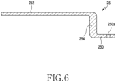
- FIG. 6 is a cross-sectional view illustrating a first heat transfer member according to various embodiments of the disclosure.
- the first heat transfer member may include a metal material, for example, a material (e.g., an aluminum material or a copper material) of which a heat transfer efficiency is higher than a designated range.
- the first heat transfer member 25 may include a plate shape which is bent at least once.
- the first heat transfer member 25 may have one portion 250 fastened to a printed circuit board (e.g., the printed circuit board 21 of FIG. 3 ) by means of a fastener, and may have the other end portion 252 coupled to a first TIM (e.g., the TIM 27 of FIG. 3 ).
- Heat generated from the printed circuit board 21 may be transferred to the TIM 27 by means of the first heat transfer member 25.
- the one end portion 250 and the other end portion 252 may be integrally coupled by means of a connection portion 254.
- the first heat transfer member 25 may be manufactured by being bent at least once.
- the one end portion 250 and the other end portion 252 may be disposed in a substantially horizontal state, and the connection portion 254 may be disposed in a substantially vertical state.
- the TIM 27 may be disposed in a state of being closely in contact with first and second heat transfer members (e.g., the first and second heat transfer members 25 and 26 of FIG. 3 ).
- a first face facing a first direction of the TIM 27 may be disposed in a state of being closely in contact with the second heat transfer member (e.g., the second heat transfer member 26 of FIG. 3 ), and a second face facing a second direction may be disposed in a state of being closely in contact with the first heat transfer member 25.
- the TIM 27 may serve for a function of transferring heat, which is transferred from the first heat transfer member 25, to the second heat transfer member 26, and may serve for a function of a connection member which couples the first and second heat transfer members 25 and 26.
- FIG. 7 is a cross-sectional view illustrating a second heat transfer member according to various embodiments of the disclosure.
- the second heat transfer member may be constructed of a metal material, for example, an aluminum material having good heat transfer efficiency.
- the second heat transfer member 26 may have a hat shape which is advantageous to collect the transferred heat and spread it to acoustic holes (e.g., the acoustic holes 110 of FIG. 1 ).
- the second heat transfer member 26 may serve for a function which collects heat transferred from a TIM (e.g., the TIM 27 of FIG. 3 ) to transfer it to a heat dissipation duct (e.g., the heat dissipation duct 33 of FIG. 5 ).
- a TIM e.g., the TIM 27 of FIG. 3
- a heat dissipation duct e.g., the heat dissipation duct 33 of FIG. 5
- it may be disposed coaxially with a power supply unit (e.g., the power supply unit 22 of FIG. 3 ) along a central axis C.
- the second heat transfer member 26 may include a first portion 260 which is closely in contact with the TIM 27, a second portion 262 which is fastened with an upper enclosure (e.g., the enclosure 20 of FIG. 3 ), and a third portion 264 which couples the first and second portions 260 and 262.
- the first and second portions 260 and 262 may be disposed in a substantially horizontal state, and the third portion 264 may be disposed in a substantially vertical state.
- the first to third portions 260, 262, and 264 may be integrally manufactured.
- the second heat transfer member 26 may have a protrusion 266 constructed in the first portion 260.
- the protrusion 266 may have a ring shape.
- the protrusion 266 according to various embodiments is not necessarily limited to being constructed in the first portion 260, and may be additionally constructed to maximize a surface area in contact with heat in the second portion 262 or the third portion 264.
- a plurality of fastening holes 262a for fastening with one portion of the upper enclosure 210 may be constructed in the second portion 262 of the second heat transfer member 26 according to various embodiments.
- an electronic device e.g., the electronic device 1000 of FIG. 1
- a housing e.g., the housing 100 of FIG. 1
- an enclosure e.g., the enclosure 20 of FIG. 2
- at least one heating element e.g., the printed circuit board 21 of FIG. 3
- a heat dissipation structure e.g., the heat dissipation structure 28 of FIG.
- the heat dissipation structure includes: at least one first heat transfer member (e.g., the first heat transfer member 25 of FIG. 5 ) coupled to the one heating element; and a second heat transfer member (e.g., the second heat transfer member 26 of FIG. 5 ) disposed at least partially on the first heat transfer member to transfer, to the heat dissipation duct, heat transferred from the first heat transfer member.
- first heat transfer member e.g., the first heat transfer member 25 of FIG. 5
- a second heat transfer member e.g., the second heat transfer member 26 of FIG. 5
- the heating element includes: a power supply unit (e.g., the power supply unit 22 of FIG. 3 ) disposed in the enclosure (e.g., the enclosure 20 of FIG. 2 ); and at least one substrate (e.g., the substrate 21 of FIG. 3 ) disposed adjacent to the power supply unit.
- a power supply unit e.g., the power supply unit 22 of FIG. 3
- the enclosure e.g., the enclosure 20 of FIG. 2
- at least one substrate e.g., the substrate 21 of FIG. 3
- At least one Thermal Interfacing Material (TIM) (e.g., the TIM 27 of FIG. 5 ) may be further disposed between the first and second heat transfer members (e.g., the first and second heat transfer members 25 and 26 of FIG. 5 ).
- TIM Thermal Interfacing Material
- the TIM (e.g., the TIM 27 of FIG. 5 ) may be closely in contact with each of the first and second heat transfer members (e.g., the first and second heat transfer members 25 and 26 of FIG. 5 ).
- the first heat transfer member (e.g., the first heat transfer member 25 of FIG. 5 ) may include: one end portion (e.g., the one end portion 250 of FIG. 6 ), which is disposed in a substantially horizontal state, in contact with the substrate; the other end portion (e.g., the other end portion 252 of FIG. 6 ), which is disposed in a substantially horizontal state, having a gap with respect to an upper face of the power supply unit (e.g., the power supply unit 22 of FIG. 3 ); and a connection portion (e.g., the connection portion 254 of FIG. 6 ), which is disposed in a substantially vertical state, constructed by being bent at each of the one end portion and the other end portion, and disposed to have a gap with respect to a side face of the power supply unit.
- one end portion e.g., the one end portion 250 of FIG. 6
- the other end portion e.g., the other end portion 252 of FIG. 6
- a connection portion e.g., the
- the other end portion (e.g., the other end portion 252 of FIG. 6 ) may be closely in contact with the TIM (e.g., the TIM 27 of FIG. 5 ).
- the second heat transfer member (e.g., the second heat transfer member 26 of FIG. 7 ) having a shape of collecting heat may include: a substantially horizontal first portion (e.g., the first portion 260 of FIG. 7 ) which is disposed closely in contact with the TIM (e.g., the TIM 27 of FIG. 5 ); a substantially horizontal second portion (e.g., the second portion 262 of FIG. 7 ) which is fastened with the enclosure; and a third portion (e.g., the third portion 264 of FIG. 7 ) which couples between the first and second portions.
- a substantially horizontal first portion e.g., the first portion 260 of FIG. 7
- the TIM 27 of FIG. 5 e.g., the TIM 27 of FIG. 5
- a substantially horizontal second portion e.g., the second portion 262 of FIG. 7
- a third portion e.g., the third portion 264 of FIG. 7
- heat transferred in the heat dissipation duct may be collected by the first and second portions (e.g., the first and second portions 260 and 262 of FIG. 7 ).
- the first portion (e.g., the first portion 260 of FIG. 7 ) may further include a ring-shaped protrusion (e.g., the protrusion 266 of FIG. 7 ).
- the protrusion e.g., the protrusion 266 of FIG. 7
- the heat dissipation duct e.g., the heat dissipation duct 33 of FIG. 5 .
- the heat dissipation duct may include: a heat collecting unit (e.g., the heat collecting unit 31 of FIG. 5 ) having a first cross-sectional area to collect heat transferred from the one or more heat transfer members (e.g., the first and second heat transfer members 25 and 26 of FIG. 5 ); and a heat transfer duct (e.g., the heat transfer duct 32 of FIG. 5 ) which dissipates heat of the heat collecting unit to the acoustic holes (e.g., the acoustic holes 110 of FIG. 1 ) and having a second cross-sectional area smaller than the first cross-sectional area.
- a heat collecting unit e.g., the heat collecting unit 31 of FIG. 5
- a heat transfer duct e.g., the heat transfer duct 32 of FIG. 5
- a second heat transfer path (e.g., the second heat transfer path P2 of FIG. 5 ) which dissipates heat generated from the power supply unit (e.g., the power supply unit 220 of FIG. 5 ) to the outside of the acoustic holes through the first heat transfer member (e.g., the first heat transfer member 25 of FIG. 5 ), the first TIM (e.g., the TIM 27 of FIG. 5 ), the second heat transfer member (e.g., the second heat transfer member 26 of FIG. 5 ), and the heat dissipation duct (e.g., the heat dissipation duct 33 of FIG. 5 )
- the first heat transfer member e.g., the first heat transfer member 25 of FIG. 5
- the first TIM e.g., the TIM 27 of FIG. 5
- the second heat transfer member e.g., the second heat transfer member 26 of FIG. 5
- the heat dissipation duct e.g., the heat dissi
- each of the first and second heat transfer members may include at least part of an aluminum material or a copper material.
- the TIM (e.g., the TIM 27 of FIG. 5 ) may include a silicon polymer material.
- the second heat transfer member (e.g., the second heat transfer member 26 of FIG. 5 ) may include a hat shape.
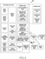
- FIG. 8 is a block diagram illustrating an electronic device 801 in a network environment 800 according to various embodiments.
- the electronic device 801 (e.g., the electronic device 1000 of FIG. 1 ) in the network environment 800 may communicate with an electronic device 802 via a first network 898 (e.g., short-range wireless communication), or an electronic device 804 or a server 808 via a second network 899 (e.g., long-range wireless communication).
- the electronic device 801 may communicate with the electronic device 804 via the server 808.
- the electronic device 801 may include a processor 820, a memory 830, an input device 850, a sound output device 855, a display device 860, an audio module 870, a sensor module 876, an interface 877, a haptic module 879, a camera module 880, a power management module 888, a battery 889, a communication module 890, a Subscriber Identification Module (SIM) 896, or an antenna module 897.
- SIM Subscriber Identification Module
- at least one (e.g., the display device 860 or the camera module 880) of the components may be omitted from the electronic device 801, or one or more other components may be added in the electronic device 801.
- some of the components may be implemented in an integrated manner, for example, as in a case of the sensor module 876 (e.g., a fingerprint sensor, an iris sensor, or an illuminance sensor) embedded in the display device 860 (e.g., a display).
- the sensor module 876 e.g., a fingerprint sensor, an iris sensor, or an illuminance sensor
- the display device 860 e.g., a display.
- the processor 820 may include a main processor 821 (e.g., a Central Processing Unit (CPU) or an Application Processor (AP)), and an auxiliary processor 823 (e.g., a Graphics Processing Unit (GPU), an Image Signal Processor (ISP), a sensor hub processor, or a Communication Processor (CP)) that is operable independently from, or in conjunction with, the main processor 821.
- auxiliary processor 823 may be adapted to consume less power than the main processor 821, or to be specific to a specified function.
- the auxiliary processor 823 may be implemented as separate from, or imbedded in the main processor 821.
- the auxiliary processor 823 may control at least some of functions or states related to at least one component (e.g., the display device 860, the sensor module 876, or the communication module 890) among the components of the electronic device 801, instead of the main processor 821 while the main processor 821 is in an inactive (e.g., sleep) state, or together with the main processor 821 while the main processor 821 is in an active state (e.g., executing an application).
- the auxiliary processor 823 e.g., an image signal processor or a communication processor
- the memory 830 may store various data, for example, software (e.g., the program 840) and input data or output data for a command related thereto, used by at least one component (e.g., the processor 820 or the sensor module 876) of the electronic device 801.
- the memory 830 may include the volatile memory 832 or the non-volatile memory 834.
- the program 840 may be stored in the memory 830 as software, and may include, for example, an Operating System (OS) 842, middleware 844, or an application 846.
- OS Operating System
- middleware 844 middleware
- application 846 application
- the input device 850 may be a device for receiving a command or data to be used by a component (e.g., the processor 820) of the electronic device 801 from the outside (e.g., a user) of the electronic device 801, and may include, for example, a microphone, a mouse, or a keyboard.
- a component e.g., the processor 820
- the input device 850 may include, for example, a microphone, a mouse, or a keyboard.
- the display device 860 may be a device for visually provide information to a user of the electronic device 801, and may include, for example, a display, a hologram device, or a projector and control circuitry to control a corresponding device. According to an embodiment, the display device 860 may include touch circuitry or a pressure sensor adapted to measure the intensity of force incurred by the touch.
- the audio module 870 may convert a sound into an electrical signal and vice versa. According to an embodiment, the audio module 870 may obtain the sound via the input device 850, or output the sound via the sound output device 855 or, for example, an external electronic device (e.g., an electronic device 802, for example, a speaker or a headphone)) wiredly or wirelessly coupled with the electronic device 801.
- an external electronic device e.g., an electronic device 802, for example, a speaker or a headphone
- the sensor module 876 may generate an electrical signal or data value corresponding to an internal operational state (e.g., power or temperature) of the electronic device 801 or an external environmental state.
- the sensor module 876 may include, for example, a gesture sensor, a gyro sensor, an atmospheric pressure sensor, a magnetic sensor, an acceleration sensor, a grip sensor, a proximity sensor, a color sensor, an Infrared (IR) sensor, a biometric sensor, a temperature sensor, a humidity sensor, or an illuminance sensor.
- IR Infrared
- the interface 877 may support a specified protocol to be coupled with the external electronic device (e.g., the electronic device 802) wiredly or wirelessly.
- the interface 877 may include, for example, a High Definition Multimedia Interface (HDMI), a Universal Serial Bus (USB) interface, a Secure Digital (SD) card interface, or an audio interface.
- HDMI High Definition Multimedia Interface
- USB Universal Serial Bus
- SD Secure Digital
- a connection terminal 878 may include a connector via which the electronic device 801 may be physically connected with the external electronic device (e.g., the electronic device 802), and may include, for example, a HDMI connector, a USB connector, an SD card connector, or an audio connector (e.g., a headphone connector),
- the haptic module 879 may convert an electrical signal into a mechanical stimulus (e.g., a vibration or a movement) or electrical stimulus which may be recognized by a user via tactile sensation or kinesthetic sensation.
- the haptic module 879 may include, for example, a motor, a piezoelectric element, or an electric stimulator.
- the camera module 880 may capture still images or moving images. According to an embodiment, the camera module 880 may include one or more lenses, image sensors, image signal processors, or flashes.
- the power management module 888 may be a module for managing power supplied to the electronic device 801, and may be implemented as at least part of, for example, a Power Management Integrated Circuit (PMIC).
- PMIC Power Management Integrated Circuit
- the battery 889 may be a device for supplying power to at least one component of the electronic device 801, and may include, for example, a primary cell which is not rechargeable, a secondary cell which is rechargeable, or a fuel cell.
- the communication module 890 may support establishing a wired communication channel or a wireless communication channel between the electronic device 801 and the external electronic device (e.g., the electronic device 802, the electronic device 804, or the server 808) and performing communication via the established communication channel.
- the communication module 890 may include one or more communication processors that are operable independently from the processor 820 (e.g., the Application Processor (AP)) and supports a wired communication or a wireless communication.
- AP Application Processor
- the communication module 890 may include a wireless communication module 892 (e.g., a cellular communication module, a short-range wireless communication module, or a Global Navigation Satellite System (GNSS) communication module) or a wired communication module 894 (e.g., a Local Area Network (LAN) communication module or a Power Line Communication (PLC) module).
- a wireless communication module 892 e.g., a cellular communication module, a short-range wireless communication module, or a Global Navigation Satellite System (GNSS) communication module
- GNSS Global Navigation Satellite System
- wired communication module 894 e.g., a Local Area Network (LAN) communication module or a Power Line Communication (PLC) module.
- LAN Local Area Network
- PLC Power Line Communication
- a corresponding one of these communication modules may communicate with the external electronic device via the first network 898 (e.g., a short-range communication network, such as Bluetooth TM , Wireless-Fidelity (Wi-Fi) direct, or Infrared Data Association (IrDA)) or the second network 899 (e.g., a long-range communication network, such as a cellular network, the Internet, or a computer network (e.g., LAN or Wide Area Network (WAN)).
- the first network 898 e.g., a short-range communication network, such as Bluetooth TM , Wireless-Fidelity (Wi-Fi) direct, or Infrared Data Association (IrDA)
- the second network 899 e.g., a long-range communication network, such as a cellular network, the Internet, or a computer network (e.g., LAN or Wide Area Network (WAN)
- These various types of the communication modules 890 may be implemented as a single chip, or may be implemented as chips separate
- the wireless communication module 892 may identify and authenticate the electronic device 801 in a communication network by using user information stored in the subscriber identification module 896.
- the antenna module 897 may include one or more antennas for transmitting or receiving a signal or power to or from the outside.
- the communication module 890 e.g., the wireless communication module 892
- At least some of the above-described components may be coupled mutually and communicate signals (e.g., commands or data) therebetween via an inter-peripheral communication scheme (e.g., a bus, General Purpose Input and Output (GPIO), Serial Peripheral Interface (SPI), or Mobile Industry Processor Interface (MIPI)).
- an inter-peripheral communication scheme e.g., a bus, General Purpose Input and Output (GPIO), Serial Peripheral Interface (SPI), or Mobile Industry Processor Interface (MIPI)).
- GPIO General Purpose Input and Output
- SPI Serial Peripheral Interface
- MIPI Mobile Industry Processor Interface
- commands or data may be transmitted or received between the electronic device 801 and the external electronic device 804 via the server 808 coupled with the second network 899.
- Each of the electronic devices 802 and 804 may be a device of a same type as, or a different type from, the electronic device 801.
- all or some of operations to be executed at the electronic device 801 may be executed at one or more of the external electronic devices.
- the electronic device 801 if the electronic device 801 should perform a function or a service automatically, or in response to a request, the electronic device 801, instead of, or in addition to, executing the function or the service, may request the one or more external electronic devices to perform at least part of the function or the service.
- the external electronic devices receiving the request may perform the requested function or an additional function, and transfer an outcome of the performing to the electronic device 801.
- the electronic device 801 may provide the requested function or service, with or without further processing of the outcome.
- a cloud computing for example, distributed computing, or client-server computing technology may be used.
- the electronic device may be one of various types of electronic devices.
- the electronic devices may include, for example, a portable communication device (e.g., a smart phone), a computer device, a portable multimedia device, a portable medical device, a camera, a wearable device, or a home appliance.
- a portable communication device e.g., a smart phone
- a computer device e.g., a laptop, a desktop, a smart phone
- portable multimedia device e.g., a portable multimedia device
- portable medical device e.g., a portable medical device
- camera e.g., a camera
- a wearable device e.g., a portable medical device
- Various embodiments of the disclosure may be implemented as software (e.g., the program 840) including instructions that are stored a storage medium (e.g., the internal memory 836 or the external memory 838) that is readable by a machine (e.g., a computer).
- the machine may include an electronic device (e.g., the electronic device 801) according to the disclosure embodiments, as a device which invokes the stored instructions from the medium and is operable according to the instruction invoked.
- the instruction When the instruction is executed by a processor (e.g., the processor 820), the processor may perform a function corresponding to the instruction by using other components directly or under the control of the processor.
- the instruction may include a code generated or executed by a complier or an interpreter.
- the machine-readable storage medium may be provided in the form of a non-transitory storage medium.
- non-transitory simply means that the storage medium is a tangible device, and does not include a signal, but this term does not differentiate between where data is semi-permanently stored in the storage medium and where the data is temporarily stored in the storage medium.
- a method may be included and provided in a computer program product.
- the computer program product may be traded as a product between a seller and a buyer.
- the computer program product may be distributed in the form of a machine-readable storage medium (e.g., compact disc read only memory (CD-ROM)), or be distributed (e.g., downloaded or uploaded) online via an application store (e.g., Play Store TM ), or between two user devices (e.g., smart phones) directly. If distributed online, at least part of the computer program product may be temporarily generated or at least temporarily stored in the machine-readable storage medium, such as memory of the manufacturer's server, a server of the application store, or a relay server.
- CD-ROM compact disc read only memory
- an application store e.g., Play Store TM
- two user devices e.g., smart phones
Landscapes
- Engineering & Computer Science (AREA)
- Physics & Mathematics (AREA)
- Acoustics & Sound (AREA)
- Signal Processing (AREA)
- Microelectronics & Electronic Packaging (AREA)
- Thermal Sciences (AREA)
- Cooling Or The Like Of Electrical Apparatus (AREA)
Description
- Various embodiments of the disclosure relate to a heat dissipation structure of an electronic device.
- The conventional electronic device may have at least one heating element such as a printed circuit board included therein, with a structure in which heat generated from the printed circuit board stays in a closed space of an enclosure since a heat dissipation structure for dissipating the heat is not provided inside the enclosure.
- Relevant prior art teaching may be found in the following documents :
KR 2003 0055812 JP 2005 136250 A - Accordingly, the conventional electronic device does not have additional heat dissipation structure for dissipating heat generated therein to the outside, which results in a problem in that heat dissipation efficiency deteriorates.
- Various embodiments of the disclosure has a heat dissipation duct and a heat dissipation structure for transferring heat generated therein to the outside of a housing, thereby providing an electronic device capable of efficiently dissipating internal heat to the outside.
- Various embodiments of the disclosure uses a low-pitch or high-pitch amplifying device to pump internal heat to the outside, thereby providing an electronic device capable of effectively dissipating the heat.
- The present invention is directed to an electronic device as defined in claim 1.
- According to various embodiments of the disclosure, heat generated from a heating element inside an electronic device can be efficiently dissipated to the outside of acoustic holes through a heat transfer path consisting of a heat dissipation structure and a heat dissipation duct.
-
-
FIG. 1 is a perspective view illustrating an exterior of an electronic device according to various embodiments of the disclosure; -
FIG. 2 is an exploded perspective view illustrating an enclosure disposed inside an electronic device according to various embodiments of the disclosure; -
FIG. 3 is an exploded perspective view illustrating an inner structure of an enclosure according to various embodiments of the disclosure; -
FIG. 4 is a cross-sectional view illustrating an inner structure of an electronic device according to various embodiments of the disclosure; -
FIG. 5 is a cross-sectional view illustrating a heat dissipation structure of an electronic device according to various embodiments of the disclosure; -
FIG. 6 is a cross-sectional view illustrating a first heat transfer member according to various embodiments of the disclosure; -
FIG. 7 is a cross-sectional view illustrating a second heat transfer member according to various embodiments of the disclosure; -
FIG. 8 is a block diagram illustrating an electronic device in a network environment according to various embodiments. -
FIG. 1 is a perspective view illustrating an exterior of an electronic device according to various embodiments of the disclosure. - Referring to
FIG. 1 , anelectronic device 1000 according to various embodiments may include a desk-type speaker which can be mounted on a desk, as a speaker capable of radiating a high-pitch or low-pitch sound. In addition, theelectronic device 1000 may be an Artificial Intelligence (AI) speaker having a built-in microphone device. - The
electronic device 1000 according to various embodiments may include ahousing 100 which constitutes an exterior and protects internal electronic components. Thehousing 100 may include anupper housing 11 and alower housing 12. Thehousing 100 may include a plurality ofleg portions 13 for mounting the device on a desk. - The
upper housing 11 according to various embodiments may have a plurality ofacoustic holes 110 constructed on an outer face. For example, each of theacoustic holes 110 may be constructed generally on theupper housing 11, and may be constructed equi-distantly. Theacoustic holes 110 may be holes for transferring a sound radiated from a sound generating device (not shown) to the outside. -
FIG. 2 is an exploded perspective view illustrating an enclosure disposed inside an electronic device according to various embodiments of the disclosure. - Referring to
FIG. 2 , a housing (e.g., thehousing 100 ofFIG. 1 ) of an electronic device (e.g., theelectronic device 1000 ofFIG. 1 ) according to various embodiments includes anenclosure 20. Theenclosure 20 according to various embodiments may be an internal housing capable of accommodating and supporting electronic components, for example, a printed circuit board, a power supply unit, or the like. Theenclosure 20 may be surrounded by upper andlower housings -
FIG. 3 is an exploded perspective view illustrating an inner structure of an enclosure according to various embodiments of the disclosure. - Referring to
FIG. 3 , an enclosure (e.g., theenclosure 20 ofFIG. 2 ) according to various embodiments may include anupper enclosure 210 and alower enclosure 212. Theupper enclosure 210 may be coupled to thelower enclosure 212 by using at least one fastening structure. Theenclosure 20 according to various embodiments includes etarte apower supply unit 22, aheat dissipation structure 28, and at least one printedcircuit board 21. - The
enclosure 20 according to various embodiments has theheat dissipation structure 28 accommodated in theupper enclosure 210. Theheat dissipation structure 28 according to various embodiments is a structure for transferring heat generated from theheating element 21 inside theenclosure 20 to the outside ofacoustic holes 110. For example, theheating element 21 includes a printed circuit board, on which a plurality of electronic components are mounted, thepower supply unit 22, or the like. The printed circuit board may include an electronic component for amplifying an audio signal. - The
heat dissipation structure 28 according to various embodiments is a structure coupled to the at least oneheating element 21 to provide a heat transfer path for dissipating heat generated from theheating element 21 to the outside of the housing, and includes at least one heat transfer member, a heat dissipation duct (e.g., aheat dissipation duct 33 ofFIG. 5 ), a Thermal Interfacing Material (TIM) 27, or the like. - The
heat dissipation structure 28 according to various embodiments is a structure which provides a heat transfer path for dissipating heat generated from a heating element to outside portion, and may be a structure capable of transferring heat generated from a high-temperature heating element to the outside (e.g., a relatively low-temperature portion). - The
heat dissipation structure 28 according to various embodiments includes first and secondheat transfer members heat transfer member 25 may be a member coupled to the printedcircuit board 21 dedicated for amplification so that heat generated from the printedcircuit board 21 dedicated for amplification is transferred to another heat transfer element. For example, the firstheat transfer member 25 may include a material (e.g., aluminum) of which a thermal conductive is higher than a designated range. - The second
heat transfer member 26 according to various embodiments may be a heat transfer element coupled to the firstheat transfer member 25 by means of the TIM so that heat generated from the firstheat transfer member 25 is transferred to a heat dissipation duct. For example, the TIM may be disposed between the first and secondheat transfer members electronic device 1000 operates. -
FIG. 4 is a cross-sectional view illustrating an inner structure of an electronic device according to various embodiments of the disclosure.FIG. 5 is a cross-sectional view illustrating a heat dissipation structure of an electronic device according to various embodiments of the disclosure. - A
heat dissipation structure 28 of anelectronic device 1000 according to various embodiments will be described with reference toFIG. 4 andFIG. 5 . - With respect to a power supply unit (e.g., the
power supply unit 22 ofFIG. 3 ) disposed coaxially with a central axis C, an electronic device according to various embodiments (e.g., theelectronic device 1000 ofFIG. 1 ) has a heat dissipation structure (e.g., theheat dissipation structure 28 ofFIG. 3 ) disposed in a first direction of apower supply unit 22 and has a heat dissipation duct (e.g., theheat dissipation duct 33 ofFIG. 5 ) located at an upper portion of theheat dissipation structure 28 to dissipation heat to the outside. - The
electronic device 1000 according to various embodiments has at least one substrate (e.g., the printedcircuit board 21 ofFIG. 3 ) disposed in an outer circumferential direction of thepower supply unit 22. For example, aprinted circuit board 21 mounted inside theenclosure 20 may include a printed circuit board for amplifying a sound, a printed circuit board related to an operation of the electronic device, a printed circuit board for operating the power supply unit, or the like. Among the plurality of printed circuit boards, the printed circuit board dedicated for amplification may be disposed adjacent to thepower supply unit 22, and may be disposed in an outer circumferential direction of thepower supply unit 22. The printedcircuit board 21 may be fastened to anenclosure 20 in a state of facing each other by means of a fastener. - The printed
circuit board 21 according to various embodiments is a first heating element, and thepower supply unit 22 is a second heating element. For example, among at least one or more printed circuit boards, heat generated from the printed circuit board dedicated for amplification is the most severe, and thus the first heating element may be the printedcircuit board 21 dedicated for amplification. Heat generated from theprinted circuit board 21 dedicated for amplification may be relatively higher than heat generated from the power supply unit. Thepower supply unit 22 may also include a printed circuit board. - According to various embodiments, at least one printed circuit board (e.g., a PCB) may include an audio signal amplifying circuit, an audio signal processing circuit, and a power supply circuit for supplying power. The circuit may be constructed as a separate printed circuit board.
- The audio signal amplifying circuit of the printed
circuit board 21 according to various embodiments may produce relatively higher heat than other circuits. The audio signal amplifying circuit or an area of the circuit may be a heating element. - In the
electronic device 1000 according to various embodiments, thepower supply unit 22 may be disposed to overlap with theheat dissipation structure 28, and the printedcircuit board 21 may be disposed not to overlap with theheat dissipation structure 28. When viewed from above theenclosure 20, thepower supply unit 22 and theheat dissipation structure 28 overlap, and the printedcircuit board 21 may not overlap with theheat dissipation structure 28. - The
heat dissipation structure 28 according to various embodiments is disposed between aheat dissipation duct 33 and thepower supply unit 22. Heat generated from thepower supply unit 22 or printedcircuit board 21 which is a heating element is transferred by means of theheat dissipation structure 28, and thereafter flows toward the outside of the plurality ofacoustic holes 110 via theheat dissipation duct 33. - Since the heat generated from the
power supply unit 22 or the printedcircuit board 21 rises upward, theheat dissipation duct 33 provided by theheat dissipation structure 28 according to an embodiment may be disposed in a direction of acoustic holes (e.g., theacoustic holes 110 ofFIG. 1 ) at an upper side of thepower supply unit 22 or printedcircuit board 21. - The
heat dissipation structure 28 according to various embodiments includes first and secondheat transfer members TIM 27. Alternatively, the heat dissipation structure may include theheat dissipation duct 33 which provides a heat transfer path. - The
heat dissipation duct 33 according to various embodiments may include aheat collecting unit 31 having a first cross-sectional area A1 and aheat transfer duct 32 having a second cross-sectional area A2. The first cross-sectional area A1 may be larger than the second cross-sectional area A2. Heat collected in theheat collecting unit 31 having the first cross-sectional area A1 is accelerated while flowing to theheat transfer duct 32 having the second cross-sectional area A2 smaller than the first cross-sectional area A1, so that the heat can be dissipated to the outside of theacoustic holes 110 with a speed. - A heating structure of the
electronic device 1000 according to various embodiments provides a first heat transfer path P1 in such a manner that heat generated from the printedcircuit board 21 is dissipated to the outside of theacoustic holes 110 via the firstheat transfer member 25, theTIM 27, the secondheat transfer member 26, and theheat dissipation duct 33, and provides a second heat transfer path P2 in such a manner that heat generated from thepower supply unit 22 is dissipated to the outside of theacoustic holes 110 via the firstheat transfer member 25, theTIM 27, the secondheat transfer member 26, and theheat dissipation duct 33. -
FIG. 6 is a cross-sectional view illustrating a first heat transfer member according to various embodiments of the disclosure. - Referring to
FIG. 6 , the first heat transfer member according to various embodiments (e.g., the firstheat transfer member 25 ofFIG. 3 ) may include a metal material, for example, a material (e.g., an aluminum material or a copper material) of which a heat transfer efficiency is higher than a designated range. The firstheat transfer member 25 may include a plate shape which is bent at least once. The firstheat transfer member 25 may have oneportion 250 fastened to a printed circuit board (e.g., the printedcircuit board 21 ofFIG. 3 ) by means of a fastener, and may have theother end portion 252 coupled to a first TIM (e.g., theTIM 27 ofFIG. 3 ). Heat generated from the printedcircuit board 21 may be transferred to theTIM 27 by means of the firstheat transfer member 25. The oneend portion 250 and theother end portion 252 may be integrally coupled by means of aconnection portion 254. The firstheat transfer member 25 may be manufactured by being bent at least once. The oneend portion 250 and theother end portion 252 may be disposed in a substantially horizontal state, and theconnection portion 254 may be disposed in a substantially vertical state. - The
TIM 27 according to various embodiments may be disposed in a state of being closely in contact with first and second heat transfer members (e.g., the first and secondheat transfer members FIG. 3 ). A first face facing a first direction of theTIM 27 may be disposed in a state of being closely in contact with the second heat transfer member (e.g., the secondheat transfer member 26 ofFIG. 3 ), and a second face facing a second direction may be disposed in a state of being closely in contact with the firstheat transfer member 25. TheTIM 27 may serve for a function of transferring heat, which is transferred from the firstheat transfer member 25, to the secondheat transfer member 26, and may serve for a function of a connection member which couples the first and secondheat transfer members -
FIG. 7 is a cross-sectional view illustrating a second heat transfer member according to various embodiments of the disclosure. - Referring to
FIG. 7 , the second heat transfer member according to various embodiments (e.g., the secondheat transfer member 26 ofFIG. 3 ) may be constructed of a metal material, for example, an aluminum material having good heat transfer efficiency. The secondheat transfer member 26 may have a hat shape which is advantageous to collect the transferred heat and spread it to acoustic holes (e.g., theacoustic holes 110 ofFIG. 1 ). - The second
heat transfer member 26 according to an embodiment may serve for a function which collects heat transferred from a TIM (e.g., theTIM 27 ofFIG. 3 ) to transfer it to a heat dissipation duct (e.g., theheat dissipation duct 33 ofFIG. 5 ). For example, it may be disposed coaxially with a power supply unit (e.g., thepower supply unit 22 ofFIG. 3 ) along a central axis C. - The second
heat transfer member 26 according to various embodiments may include afirst portion 260 which is closely in contact with theTIM 27, asecond portion 262 which is fastened with an upper enclosure (e.g., theenclosure 20 ofFIG. 3 ), and athird portion 264 which couples the first andsecond portions second portions third portion 264 may be disposed in a substantially vertical state. For example, the first tothird portions - The second
heat transfer member 26 according to various embodiments may have aprotrusion 266 constructed in thefirst portion 260. For example theprotrusion 266 may have a ring shape. - The
protrusion 266 according to various embodiments is not necessarily limited to being constructed in thefirst portion 260, and may be additionally constructed to maximize a surface area in contact with heat in thesecond portion 262 or thethird portion 264. A plurality offastening holes 262a for fastening with one portion of theupper enclosure 210 may be constructed in thesecond portion 262 of the secondheat transfer member 26 according to various embodiments. - According to various embodiments, an electronic device (e.g., the
electronic device 1000 ofFIG. 1 ) includes : a housing (e.g., thehousing 100 ofFIG. 1 ) including a plurality of acoustic holes (e.g., theacoustic holes 110 ofFIG. 1 ); an enclosure (e.g., theenclosure 20 ofFIG. 2 ) mounted in the housing; at least one heating element (e.g., the printedcircuit board 21 ofFIG. 3 ) disposed in the enclosure; a heat dissipation structure (e.g., theheat dissipation structure 28 ofFIG. 3 ) disposed on the heating element to transfer heat generated from the heating element; and a heat dissipation duct (e.g., theheat dissipation duct 33 ofFIG. 5 ) disposed at least partially on the heat dissipation structure to provide a path for transferring the heat transferred from the heat dissipation structure to the outside through the acoustic holes. The heat dissipation structure includes: at least one first heat transfer member (e.g., the firstheat transfer member 25 ofFIG. 5 ) coupled to the one heating element; and a second heat transfer member (e.g., the secondheat transfer member 26 ofFIG. 5 ) disposed at least partially on the first heat transfer member to transfer, to the heat dissipation duct, heat transferred from the first heat transfer member. - According to various embodiments, the heating element includes: a power supply unit (e.g., the
power supply unit 22 ofFIG. 3 ) disposed in the enclosure (e.g., theenclosure 20 ofFIG. 2 ); and at least one substrate (e.g., thesubstrate 21 ofFIG. 3 ) disposed adjacent to the power supply unit. - According to various embodiments, at least one Thermal Interfacing Material (TIM) (e.g., the
TIM 27 ofFIG. 5 ) may be further disposed between the first and second heat transfer members (e.g., the first and secondheat transfer members FIG. 5 ). - According to various embodiments, the TIM (e.g., the
TIM 27 ofFIG. 5 ) may be closely in contact with each of the first and second heat transfer members (e.g., the first and secondheat transfer members FIG. 5 ). - According to various embodiments, the first heat transfer member (e.g., the first
heat transfer member 25 ofFIG. 5 ) may include: one end portion (e.g., the oneend portion 250 ofFIG. 6 ), which is disposed in a substantially horizontal state, in contact with the substrate; the other end portion (e.g., theother end portion 252 ofFIG. 6 ), which is disposed in a substantially horizontal state, having a gap with respect to an upper face of the power supply unit (e.g., thepower supply unit 22 ofFIG. 3 ); and a connection portion (e.g., theconnection portion 254 ofFIG. 6 ), which is disposed in a substantially vertical state, constructed by being bent at each of the one end portion and the other end portion, and disposed to have a gap with respect to a side face of the power supply unit. - According to various embodiments, the other end portion (e.g., the
other end portion 252 ofFIG. 6 ) may be closely in contact with the TIM (e.g., theTIM 27 ofFIG. 5 ). - According to various embodiments, the second heat transfer member (e.g., the second
heat transfer member 26 ofFIG. 7 ) having a shape of collecting heat may include: a substantially horizontal first portion (e.g., thefirst portion 260 ofFIG. 7 ) which is disposed closely in contact with the TIM (e.g., theTIM 27 ofFIG. 5 ); a substantially horizontal second portion (e.g., thesecond portion 262 ofFIG. 7 ) which is fastened with the enclosure; and a third portion (e.g., thethird portion 264 ofFIG. 7 ) which couples between the first and second portions. - According to various embodiments, heat transferred in the heat dissipation duct (e.g., the
heat dissipation duct 33 ofFIG. 5 ) may be collected by the first and second portions (e.g., the first andsecond portions FIG. 7 ). - According to various embodiments, the first portion (e.g., the
first portion 260 ofFIG. 7 ) may further include a ring-shaped protrusion (e.g., theprotrusion 266 ofFIG. 7 ). - According to various embodiments, the protrusion (e.g., the
protrusion 266 ofFIG. 7 ) may protrude towards the heat dissipation duct (e.g., theheat dissipation duct 33 ofFIG. 5 ). - According to various embodiments, the heat dissipation duct (e.g., the
heat dissipation duct 33 ofFIG. 5 ) may include: a heat collecting unit (e.g., theheat collecting unit 31 ofFIG. 5 ) having a first cross-sectional area to collect heat transferred from the one or more heat transfer members (e.g., the first and secondheat transfer members FIG. 5 ); and a heat transfer duct (e.g., theheat transfer duct 32 ofFIG. 5 ) which dissipates heat of the heat collecting unit to the acoustic holes (e.g., theacoustic holes 110 ofFIG. 1 ) and having a second cross-sectional area smaller than the first cross-sectional area. - According to various embodiments, the electronic device includes a first heat transfer path (e.g., the first heat transfer path P1 of
FIG. 5 ) which dissipates heat generated from the substrate (e.g., thesubstrate 210 ofFIG. 3 ) to the outside of the acoustic holes (e.g., theacoustic holes 110 ofFIG. 1 ) through the first heat transfer member (e.g., the firstheat transfer member 25 ofFIG. 5 ), the TIM (e.g., theTIM 27 ofFIG. 5 ), the second heat transfer member (e.g., the secondheat transfer member 26 ofFIG. 5 ), and the heat dissipation duct (e.g., theheat dissipation duct 33 ofFIG. 5 ); and a second heat transfer path (e.g., the second heat transfer path P2 ofFIG. 5 ) which dissipates heat generated from the power supply unit (e.g., the power supply unit 220 ofFIG. 5 ) to the outside of the acoustic holes through the first heat transfer member (e.g., the firstheat transfer member 25 ofFIG. 5 ), the first TIM (e.g., theTIM 27 ofFIG. 5 ), the second heat transfer member (e.g., the secondheat transfer member 26 ofFIG. 5 ), and the heat dissipation duct (e.g., theheat dissipation duct 33 ofFIG. 5 ) - According to various embodiments, each of the first and second heat transfer members (e.g., the first and second
heat transfer members FIG. 5 ) may include at least part of an aluminum material or a copper material. - According to various embodiments, the TIM (e.g., the
TIM 27 ofFIG. 5 ) may include a silicon polymer material. - According to various embodiments, the second heat transfer member (e.g., the second
heat transfer member 26 ofFIG. 5 ) may include a hat shape. -
FIG. 8 is a block diagram illustrating anelectronic device 801 in anetwork environment 800 according to various embodiments. - Referring to
FIG. 8 , the electronic device 801 (e.g., theelectronic device 1000 ofFIG. 1 ) in thenetwork environment 800 may communicate with anelectronic device 802 via a first network 898 (e.g., short-range wireless communication), or anelectronic device 804 or aserver 808 via a second network 899 (e.g., long-range wireless communication). According to an embodiment, theelectronic device 801 may communicate with theelectronic device 804 via theserver 808. According to an embodiment, theelectronic device 801 may include aprocessor 820, amemory 830, aninput device 850, asound output device 855, adisplay device 860, anaudio module 870, asensor module 876, aninterface 877, ahaptic module 879, acamera module 880, apower management module 888, abattery 889, acommunication module 890, a Subscriber Identification Module (SIM) 896, or anantenna module 897. In some embodiments, at least one (e.g., thedisplay device 860 or the camera module 880) of the components may be omitted from theelectronic device 801, or one or more other components may be added in theelectronic device 801. In some embodiments, some of the components may be implemented in an integrated manner, for example, as in a case of the sensor module 876 (e.g., a fingerprint sensor, an iris sensor, or an illuminance sensor) embedded in the display device 860 (e.g., a display). - The
processor 820 may drive, for example, software (e.g., a program 840) to control at least one other component (e.g., a hardware or software component) of theelectronic device 801 coupled with theprocessor 820, and may perform various data processing or computation. Theprocessor 820 may load a command or data received from other components (e.g., thesensor module 876 or the communication module 890) in avolatile memory 832, process the command or the data stored in thevolatile memory 832, and store resulting data in anon-volatile memory 834. According to an embodiment, theprocessor 820 may include a main processor 821 (e.g., a Central Processing Unit (CPU) or an Application Processor (AP)), and an auxiliary processor 823 (e.g., a Graphics Processing Unit (GPU), an Image Signal Processor (ISP), a sensor hub processor, or a Communication Processor (CP)) that is operable independently from, or in conjunction with, themain processor 821. Additionally or alternatively, theauxiliary processor 823 may be adapted to consume less power than themain processor 821, or to be specific to a specified function. Herein, theauxiliary processor 823 may be implemented as separate from, or imbedded in themain processor 821. - In this case, the
auxiliary processor 823 may control at least some of functions or states related to at least one component (e.g., thedisplay device 860, thesensor module 876, or the communication module 890) among the components of theelectronic device 801, instead of themain processor 821 while themain processor 821 is in an inactive (e.g., sleep) state, or together with themain processor 821 while themain processor 821 is in an active state (e.g., executing an application). According to an embodiment, the auxiliary processor 823 (e.g., an image signal processor or a communication processor) may be implemented as part of another component (e.g., thecamera module 880 or the communication module 890) functionally related to theauxiliary processor 823. Thememory 830 may store various data, for example, software (e.g., the program 840) and input data or output data for a command related thereto, used by at least one component (e.g., theprocessor 820 or the sensor module 876) of theelectronic device 801. Thememory 830 may include thevolatile memory 832 or thenon-volatile memory 834. - The
program 840 may be stored in thememory 830 as software, and may include, for example, an Operating System (OS) 842,middleware 844, or anapplication 846. - The
input device 850 may be a device for receiving a command or data to be used by a component (e.g., the processor 820) of theelectronic device 801 from the outside (e.g., a user) of theelectronic device 801, and may include, for example, a microphone, a mouse, or a keyboard. - The
sound output device 855 may be a device for outputting sound signals to the outside of theelectronic device 801, and may include, for example, a speaker or a receiver. The speaker may be used for general purposes, such as playing multimedia or playing record, and the receiver may be used for incoming calls. According to an embodiment, the receiver may be implemented as separate from, or as part of the speaker. - The
display device 860 may be a device for visually provide information to a user of theelectronic device 801, and may include, for example, a display, a hologram device, or a projector and control circuitry to control a corresponding device. According to an embodiment, thedisplay device 860 may include touch circuitry or a pressure sensor adapted to measure the intensity of force incurred by the touch. - The
audio module 870 may convert a sound into an electrical signal and vice versa. According to an embodiment, theaudio module 870 may obtain the sound via theinput device 850, or output the sound via thesound output device 855 or, for example, an external electronic device (e.g., anelectronic device 802, for example, a speaker or a headphone)) wiredly or wirelessly coupled with theelectronic device 801. - The
sensor module 876 may generate an electrical signal or data value corresponding to an internal operational state (e.g., power or temperature) of theelectronic device 801 or an external environmental state. Thesensor module 876 may include, for example, a gesture sensor, a gyro sensor, an atmospheric pressure sensor, a magnetic sensor, an acceleration sensor, a grip sensor, a proximity sensor, a color sensor, an Infrared (IR) sensor, a biometric sensor, a temperature sensor, a humidity sensor, or an illuminance sensor. - The
interface 877 may support a specified protocol to be coupled with the external electronic device (e.g., the electronic device 802) wiredly or wirelessly. According to an embodiment, theinterface 877 may include, for example, a High Definition Multimedia Interface (HDMI), a Universal Serial Bus (USB) interface, a Secure Digital (SD) card interface, or an audio interface. - A
connection terminal 878 may include a connector via which theelectronic device 801 may be physically connected with the external electronic device (e.g., the electronic device 802), and may include, for example, a HDMI connector, a USB connector, an SD card connector, or an audio connector (e.g., a headphone connector), - The
haptic module 879 may convert an electrical signal into a mechanical stimulus (e.g., a vibration or a movement) or electrical stimulus which may be recognized by a user via tactile sensation or kinesthetic sensation. Thehaptic module 879 may include, for example, a motor, a piezoelectric element, or an electric stimulator. - The
camera module 880 may capture still images or moving images. According to an embodiment, thecamera module 880 may include one or more lenses, image sensors, image signal processors, or flashes. - The
power management module 888 may be a module for managing power supplied to theelectronic device 801, and may be implemented as at least part of, for example, a Power Management Integrated Circuit (PMIC). - The
battery 889 may be a device for supplying power to at least one component of theelectronic device 801, and may include, for example, a primary cell which is not rechargeable, a secondary cell which is rechargeable, or a fuel cell. - The
communication module 890 may support establishing a wired communication channel or a wireless communication channel between theelectronic device 801 and the external electronic device (e.g., theelectronic device 802, theelectronic device 804, or the server 808) and performing communication via the established communication channel. Thecommunication module 890 may include one or more communication processors that are operable independently from the processor 820 (e.g., the Application Processor (AP)) and supports a wired communication or a wireless communication. According to an embodiment, thecommunication module 890 may include a wireless communication module 892 (e.g., a cellular communication module, a short-range wireless communication module, or a Global Navigation Satellite System (GNSS) communication module) or a wired communication module 894 (e.g., a Local Area Network (LAN) communication module or a Power Line Communication (PLC) module). A corresponding one of these communication modules may communicate with the external electronic device via the first network 898 (e.g., a short-range communication network, such as Bluetooth™, Wireless-Fidelity (Wi-Fi) direct, or Infrared Data Association (IrDA)) or the second network 899 (e.g., a long-range communication network, such as a cellular network, the Internet, or a computer network (e.g., LAN or Wide Area Network (WAN)). These various types of thecommunication modules 890 may be implemented as a single chip, or may be implemented as chips separate from each other. - According to an embodiment, the wireless communication module 892 may identify and authenticate the
electronic device 801 in a communication network by using user information stored in thesubscriber identification module 896. - The
antenna module 897 may include one or more antennas for transmitting or receiving a signal or power to or from the outside. According to an embodiment, the communication module 890 (e.g., the wireless communication module 892) may transmit or receive a signal to or from the external electronic device via an antenna appropriate for a communication scheme. - At least some of the above-described components may be coupled mutually and communicate signals (e.g., commands or data) therebetween via an inter-peripheral communication scheme (e.g., a bus, General Purpose Input and Output (GPIO), Serial Peripheral Interface (SPI), or Mobile Industry Processor Interface (MIPI)).
- According to an embodiment, commands or data may be transmitted or received between the
electronic device 801 and the externalelectronic device 804 via theserver 808 coupled with thesecond network 899. Each of theelectronic devices electronic device 801. According to an embodiment, all or some of operations to be executed at theelectronic device 801 may be executed at one or more of the external electronic devices. According to an embodiment, if theelectronic device 801 should perform a function or a service automatically, or in response to a request, theelectronic device 801, instead of, or in addition to, executing the function or the service, may request the one or more external electronic devices to perform at least part of the function or the service. The external electronic devices receiving the request may perform the requested function or an additional function, and transfer an outcome of the performing to theelectronic device 801. Theelectronic device 801 may provide the requested function or service, with or without further processing of the outcome. To that end, a cloud computing, for example, distributed computing, or client-server computing technology may be used. - The electronic device according to various embodiments disclosed in the disclosure may be one of various types of electronic devices. The electronic devices may include, for example, a portable communication device (e.g., a smart phone), a computer device, a portable multimedia device, a portable medical device, a camera, a wearable device, or a home appliance. According to an embodiment of the disclosure, the electronic device is not limited to the aforementioned devices.
- Various embodiments of the disclosure may be implemented as software (e.g., the program 840) including instructions that are stored a storage medium (e.g., the
internal memory 836 or the external memory 838) that is readable by a machine (e.g., a computer). The machine may include an electronic device (e.g., the electronic device 801) according to the disclosure embodiments, as a device which invokes the stored instructions from the medium and is operable according to the instruction invoked. When the instruction is executed by a processor (e.g., the processor 820), the processor may perform a function corresponding to the instruction by using other components directly or under the control of the processor. The instruction may include a code generated or executed by a complier or an interpreter. The machine-readable storage medium may be provided in the form of a non-transitory storage medium. Herein, the term "non-transitory" simply means that the storage medium is a tangible device, and does not include a signal, but this term does not differentiate between where data is semi-permanently stored in the storage medium and where the data is temporarily stored in the storage medium. - According to an embodiment, a method according to various embodiments of the disclosure may be included and provided in a computer program product. The computer program product may be traded as a product between a seller and a buyer. The computer program product may be distributed in the form of a machine-readable storage medium (e.g., compact disc read only memory (CD-ROM)), or be distributed (e.g., downloaded or uploaded) online via an application store (e.g., Play Store™), or between two user devices (e.g., smart phones) directly. If distributed online, at least part of the computer program product may be temporarily generated or at least temporarily stored in the machine-readable storage medium, such as memory of the manufacturer's server, a server of the application store, or a relay server.
Claims (13)
- An electronic device (1000) comprising:a housing (200) including a plurality of acoustic holes (110);an enclosure (20) mounted in the housing (200); two heating elements disposed in the enclosure (20), comprisinga power supply unit (22) disposed in the enclosure, coaxially with a central axis (C) of the device; andat least one substrate (21) disposed adjacent to the power supply unit (22) in an outer circumferential direction of the power supply unit (22);a heat dissipation structure (28) disposed on the heating elements to transfer heat generated from the heating elements; anda heat dissipation duct (33) disposed at least partially on the heat dissipation structure (28) to provide a path for transferring the heat transferred from the heat dissipation structure (28) to the outside through the acoustic holes (110),wherein the heat dissipation structure (28) comprises:at least one first heat transfer member (25) coupled to the substrate (21); anda second heat transfer member (26) disposed at least partially on the first heat transfer member (25) to transfer, to the heat dissipation duct (33), heat transferred from the first heat transfer member (25).
- The electronic device (1000) of claim 1, wherein at least one Thermal Interfacing Material TIM, (27) is further disposed between the first and second heat transfer members (25, 26).
- The electronic device (1000) of claim 2, wherein the TIM (27) is closely in contact with each of the first and second heat transfer members (25, 26).
- The electronic device (1000) of claim 1, wherein the first heat transfer member (25) comprises:one end portion (250), which is disposed in a substantially horizontal state, in contact with the substrate;the other end portion (252), which is disposed in a substantially horizontal state having a gap with respect to an upper face of the power supply unit (22); anda connection portion (254), which is disposed in a substantially vertical state, constructed by being bent at each of the one end portion (250) and the other end portion (252), and disposed to have a gap with respect to a side face of the power supply unit (22).
- The electronic device (1000) of claim 2 or 3 and 4, wherein the other end portion (252) is closely in contact with the TIM (27).
- The electronic device of any of the previous claims, wherein the second heat transfer member has a hat shape which is advantageous to collect the transferred heat and spread it to the acoustic holes.
- The electronic device (1000) of claim 2 and 6, wherein the second heat transfer member (26) having a hat shape which is advantageous to collect the transferred heat and spread it to the acoustic holes comprises:a substantially horizontal first portion (260) which is disposed closely in contact with the TIM (27);a substantially horizontal second portion (262) which is fastened with the enclosure; anda third portion (264) which couples between the first and second portions (260, 262).
- The electronic device (1000) of claim 7, wherein the first portion (260) further comprises a ring-shaped protrusion (266).
- The electronic device (1000) of claim 8, wherein the protrusion (266) protrudes towards the heat dissipation duct (33).
- The electronic device (1000) of claim 1, wherein the heat dissipation duct (33) comprises;a heat collecting unit (31) having a first cross-sectional area to collect heat transferred from the one or more heat transfer members; anda heat transfer duct (32) which dissipates heat of the heat collecting unit (31) to the acoustic holes (110) and having a second cross-sectional area smaller than the first cross-sectional area.
- The electronic device (1000) of claim 2, further comprising:a first heat transfer path (P1) which dissipates heat generated from the substrate (21) to the outside of the acoustic holes (110) through the first heat transfer member (25), the TIM (27), the second heat transfer member (26), and the heat dissipation duct (33); anda second heat transfer path (P2) which dissipates heat generated from the power supply unit (22) to the outside of the acoustic holes (110) through the first heat transfer member (25), the TIM (27), the second heat transfer member (26), and the heat dissipation duct (33).
- The electronic device (1000) of claim 1, wherein each of the first and second heat transfer members (25, 26) includes at least part of an aluminum material or a copper material.
- The electronic device (1000) of claim 2, wherein the TIM (27) includes a silicon polymer material.
Applications Claiming Priority (2)
| Application Number | Priority Date | Filing Date | Title |
|---|---|---|---|
| KR1020180091204A KR102613661B1 (en) | 2018-08-06 | 2018-08-06 | Electronic device with heat radiating structure |
| PCT/KR2019/007566 WO2020032385A1 (en) | 2018-08-06 | 2019-06-24 | Electronic device including heat dissipation structure |
Publications (3)
| Publication Number | Publication Date |
|---|---|
| EP3823303A1 EP3823303A1 (en) | 2021-05-19 |
| EP3823303A4 EP3823303A4 (en) | 2021-09-29 |
| EP3823303B1 true EP3823303B1 (en) | 2023-09-06 |
Family
ID=69415266
Family Applications (1)
| Application Number | Title | Priority Date | Filing Date |
|---|---|---|---|
| EP19848656.5A Active EP3823303B1 (en) | 2018-08-06 | 2019-06-24 | Electronic device including heat dissipation structure |
Country Status (4)
| Country | Link |
|---|---|
| US (1) | US11388841B2 (en) |
| EP (1) | EP3823303B1 (en) |
| KR (1) | KR102613661B1 (en) |
| WO (1) | WO2020032385A1 (en) |
Family Cites Families (12)
| Publication number | Priority date | Publication date | Assignee | Title |
|---|---|---|---|---|
| US4914551A (en) * | 1988-07-13 | 1990-04-03 | International Business Machines Corporation | Electronic package with heat spreader member |
| KR20030055812A (en) * | 2001-12-27 | 2003-07-04 | 에스텍 주식회사 | Heat-emitting structure of speaker system for attaching amp |
| JP4501409B2 (en) * | 2003-10-31 | 2010-07-14 | ソニー株式会社 | Heat dissipation device and electronic device |
| US7262369B1 (en) * | 2006-03-09 | 2007-08-28 | Laird Technologies, Inc. | Combined board level EMI shielding and thermal management |
| KR20120027737A (en) * | 2010-09-13 | 2012-03-22 | 현대모비스 주식회사 | Heat sink for external amplifier |
| KR20130099688A (en) | 2012-02-29 | 2013-09-06 | 주식회사 팬택 | Mobile communication device and heat exhausting method therein |
| US9282656B2 (en) | 2012-06-08 | 2016-03-08 | Apple Inc. | Gaskets for thermal ducting around heat pipes |
| CN103686550B (en) | 2013-11-18 | 2017-09-29 | 歌尔股份有限公司 | Loudspeaker module |
| CN104902358B (en) | 2015-06-08 | 2019-01-18 | 歌尔股份有限公司 | A kind of loudspeaker mould group |
| US10721837B2 (en) * | 2016-11-18 | 2020-07-21 | Lg Electronics Inc. | Mobile terminal |
| CN106792335B (en) * | 2017-01-05 | 2019-09-06 | 联想(北京)有限公司 | A kind of electronic equipment |
| US10306356B2 (en) * | 2017-03-31 | 2019-05-28 | Bose Corporation | Acoustic deflector as heat sink |
-
2018
- 2018-08-06 KR KR1020180091204A patent/KR102613661B1/en active Active
-
2019
- 2019-06-24 WO PCT/KR2019/007566 patent/WO2020032385A1/en not_active Ceased
- 2019-06-24 US US17/266,355 patent/US11388841B2/en active Active
- 2019-06-24 EP EP19848656.5A patent/EP3823303B1/en active Active
Also Published As
| Publication number | Publication date |
|---|---|
| EP3823303A1 (en) | 2021-05-19 |
| US11388841B2 (en) | 2022-07-12 |
| EP3823303A4 (en) | 2021-09-29 |
| WO2020032385A1 (en) | 2020-02-13 |
| KR102613661B1 (en) | 2023-12-14 |
| US20210321540A1 (en) | 2021-10-14 |
| KR20200016024A (en) | 2020-02-14 |
Similar Documents
| Publication | Publication Date | Title |
|---|---|---|
| CN112639668B (en) | Auxiliary control electronic device of mobile terminal | |
| US11294429B2 (en) | Flexible display device including heat dissipation structure | |
| US12016158B2 (en) | Heat radiating structure and electronic device including same | |
| US11357142B2 (en) | Electronic device including a shielding sheet and a heat radiation member | |
| US11901610B2 (en) | Electronic apparatus including antenna module | |
| US12057619B2 (en) | Electronic device having side key comprising antenna | |
| CN111614805B (en) | Electronic device | |
| KR102721373B1 (en) | Electronic device having a thermal spreading structure | |
| US11079796B2 (en) | Electronic device including flexible printed circuit board adjacent to antenna | |
| US10879506B2 (en) | Battery mounting structure and electronic device having the same | |
| US10681439B2 (en) | Electronic device including heat radiating structure | |
| US20240031727A1 (en) | Headset including in-ear microphone | |
| KR102693704B1 (en) | Portable electronic device and method for expanding space in main body of the same | |
| KR102773459B1 (en) | Electronic device including antenna | |
| US11388841B2 (en) | Electronic device including heat dissipation structure | |
| US11700324B2 (en) | Electronic device having connection path between buck converters | |
| US12051851B2 (en) | Electronic device including antenna including coupling-feeding structure | |
| US11438690B2 (en) | Vibration generating element assembly and electronic device including the same | |
| US20250194062A1 (en) | Electronic device comprising structure for dissipating heat to outside |
Legal Events
| Date | Code | Title | Description |
|---|---|---|---|
| STAA | Information on the status of an ep patent application or granted ep patent |
Free format text: STATUS: THE INTERNATIONAL PUBLICATION HAS BEEN MADE |
|
| PUAI | Public reference made under article 153(3) epc to a published international application that has entered the european phase |
Free format text: ORIGINAL CODE: 0009012 |
|
| STAA | Information on the status of an ep patent application or granted ep patent |
Free format text: STATUS: REQUEST FOR EXAMINATION WAS MADE |
|
| 17P | Request for examination filed |
Effective date: 20210210 |
|
| AK | Designated contracting states |
Kind code of ref document: A1 Designated state(s): AL AT BE BG CH CY CZ DE DK EE ES FI FR GB GR HR HU IE IS IT LI LT LU LV MC MK MT NL NO PL PT RO RS SE SI SK SM TR |
|
| A4 | Supplementary search report drawn up and despatched |
Effective date: 20210826 |
|
| RIC1 | Information provided on ipc code assigned before grant |
Ipc: H05K 7/20 20060101ALI20210820BHEP Ipc: H04R 9/02 20060101AFI20210820BHEP |
|
| DAV | Request for validation of the european patent (deleted) | ||
| DAX | Request for extension of the european patent (deleted) | ||
| GRAP | Despatch of communication of intention to grant a patent |
Free format text: ORIGINAL CODE: EPIDOSNIGR1 |
|
| STAA | Information on the status of an ep patent application or granted ep patent |
Free format text: STATUS: GRANT OF PATENT IS INTENDED |
|
| INTG | Intention to grant announced |
Effective date: 20230327 |
|
| GRAS | Grant fee paid |
Free format text: ORIGINAL CODE: EPIDOSNIGR3 |
|
| GRAA | (expected) grant |
Free format text: ORIGINAL CODE: 0009210 |
|
| STAA | Information on the status of an ep patent application or granted ep patent |
Free format text: STATUS: THE PATENT HAS BEEN GRANTED |
|
| AK | Designated contracting states |
Kind code of ref document: B1 Designated state(s): AL AT BE BG CH CY CZ DE DK EE ES FI FR GB GR HR HU IE IS IT LI LT LU LV MC MK MT NL NO PL PT RO RS SE SI SK SM TR |
|
| REG | Reference to a national code |
Ref country code: GB Ref legal event code: FG4D |
|
| REG | Reference to a national code |
Ref country code: CH Ref legal event code: EP |
|
| REG | Reference to a national code |
Ref country code: IE Ref legal event code: FG4D |
|
| REG | Reference to a national code |
Ref country code: DE Ref legal event code: R096 Ref document number: 602019037067 Country of ref document: DE |
|
| REG | Reference to a national code |
Ref country code: NL Ref legal event code: FP |
|
| REG | Reference to a national code |
Ref country code: LT Ref legal event code: MG9D |
|
| PG25 | Lapsed in a contracting state [announced via postgrant information from national office to epo] |
Ref country code: GR Free format text: LAPSE BECAUSE OF FAILURE TO SUBMIT A TRANSLATION OF THE DESCRIPTION OR TO PAY THE FEE WITHIN THE PRESCRIBED TIME-LIMIT Effective date: 20231207 |
|
| PG25 | Lapsed in a contracting state [announced via postgrant information from national office to epo] |
Ref country code: SE Free format text: LAPSE BECAUSE OF FAILURE TO SUBMIT A TRANSLATION OF THE DESCRIPTION OR TO PAY THE FEE WITHIN THE PRESCRIBED TIME-LIMIT Effective date: 20230906 Ref country code: RS Free format text: LAPSE BECAUSE OF FAILURE TO SUBMIT A TRANSLATION OF THE DESCRIPTION OR TO PAY THE FEE WITHIN THE PRESCRIBED TIME-LIMIT Effective date: 20230906 Ref country code: NO Free format text: LAPSE BECAUSE OF FAILURE TO SUBMIT A TRANSLATION OF THE DESCRIPTION OR TO PAY THE FEE WITHIN THE PRESCRIBED TIME-LIMIT Effective date: 20231206 Ref country code: LV Free format text: LAPSE BECAUSE OF FAILURE TO SUBMIT A TRANSLATION OF THE DESCRIPTION OR TO PAY THE FEE WITHIN THE PRESCRIBED TIME-LIMIT Effective date: 20230906 Ref country code: LT Free format text: LAPSE BECAUSE OF FAILURE TO SUBMIT A TRANSLATION OF THE DESCRIPTION OR TO PAY THE FEE WITHIN THE PRESCRIBED TIME-LIMIT Effective date: 20230906 Ref country code: HR Free format text: LAPSE BECAUSE OF FAILURE TO SUBMIT A TRANSLATION OF THE DESCRIPTION OR TO PAY THE FEE WITHIN THE PRESCRIBED TIME-LIMIT Effective date: 20230906 Ref country code: GR Free format text: LAPSE BECAUSE OF FAILURE TO SUBMIT A TRANSLATION OF THE DESCRIPTION OR TO PAY THE FEE WITHIN THE PRESCRIBED TIME-LIMIT Effective date: 20231207 Ref country code: FI Free format text: LAPSE BECAUSE OF FAILURE TO SUBMIT A TRANSLATION OF THE DESCRIPTION OR TO PAY THE FEE WITHIN THE PRESCRIBED TIME-LIMIT Effective date: 20230906 |
|
| REG | Reference to a national code |
Ref country code: AT Ref legal event code: MK05 Ref document number: 1610145 Country of ref document: AT Kind code of ref document: T Effective date: 20230906 |
|
| PG25 | Lapsed in a contracting state [announced via postgrant information from national office to epo] |
Ref country code: IS Free format text: LAPSE BECAUSE OF FAILURE TO SUBMIT A TRANSLATION OF THE DESCRIPTION OR TO PAY THE FEE WITHIN THE PRESCRIBED TIME-LIMIT Effective date: 20240106 |
|
| PG25 | Lapsed in a contracting state [announced via postgrant information from national office to epo] |
Ref country code: AT Free format text: LAPSE BECAUSE OF FAILURE TO SUBMIT A TRANSLATION OF THE DESCRIPTION OR TO PAY THE FEE WITHIN THE PRESCRIBED TIME-LIMIT Effective date: 20230906 |
|
| PG25 | Lapsed in a contracting state [announced via postgrant information from national office to epo] |
Ref country code: ES Free format text: LAPSE BECAUSE OF FAILURE TO SUBMIT A TRANSLATION OF THE DESCRIPTION OR TO PAY THE FEE WITHIN THE PRESCRIBED TIME-LIMIT Effective date: 20230906 |
|
| PG25 | Lapsed in a contracting state [announced via postgrant information from national office to epo] |
Ref country code: SM Free format text: LAPSE BECAUSE OF FAILURE TO SUBMIT A TRANSLATION OF THE DESCRIPTION OR TO PAY THE FEE WITHIN THE PRESCRIBED TIME-LIMIT Effective date: 20230906 Ref country code: RO Free format text: LAPSE BECAUSE OF FAILURE TO SUBMIT A TRANSLATION OF THE DESCRIPTION OR TO PAY THE FEE WITHIN THE PRESCRIBED TIME-LIMIT Effective date: 20230906 Ref country code: IS Free format text: LAPSE BECAUSE OF FAILURE TO SUBMIT A TRANSLATION OF THE DESCRIPTION OR TO PAY THE FEE WITHIN THE PRESCRIBED TIME-LIMIT Effective date: 20240106 Ref country code: ES Free format text: LAPSE BECAUSE OF FAILURE TO SUBMIT A TRANSLATION OF THE DESCRIPTION OR TO PAY THE FEE WITHIN THE PRESCRIBED TIME-LIMIT Effective date: 20230906 Ref country code: EE Free format text: LAPSE BECAUSE OF FAILURE TO SUBMIT A TRANSLATION OF THE DESCRIPTION OR TO PAY THE FEE WITHIN THE PRESCRIBED TIME-LIMIT Effective date: 20230906 Ref country code: CZ Free format text: LAPSE BECAUSE OF FAILURE TO SUBMIT A TRANSLATION OF THE DESCRIPTION OR TO PAY THE FEE WITHIN THE PRESCRIBED TIME-LIMIT Effective date: 20230906 Ref country code: AT Free format text: LAPSE BECAUSE OF FAILURE TO SUBMIT A TRANSLATION OF THE DESCRIPTION OR TO PAY THE FEE WITHIN THE PRESCRIBED TIME-LIMIT Effective date: 20230906 Ref country code: PT Free format text: LAPSE BECAUSE OF FAILURE TO SUBMIT A TRANSLATION OF THE DESCRIPTION OR TO PAY THE FEE WITHIN THE PRESCRIBED TIME-LIMIT Effective date: 20240108 Ref country code: SK Free format text: LAPSE BECAUSE OF FAILURE TO SUBMIT A TRANSLATION OF THE DESCRIPTION OR TO PAY THE FEE WITHIN THE PRESCRIBED TIME-LIMIT Effective date: 20230906 |
|
| PG25 | Lapsed in a contracting state [announced via postgrant information from national office to epo] |
Ref country code: PL Free format text: LAPSE BECAUSE OF FAILURE TO SUBMIT A TRANSLATION OF THE DESCRIPTION OR TO PAY THE FEE WITHIN THE PRESCRIBED TIME-LIMIT Effective date: 20230906 Ref country code: IT Free format text: LAPSE BECAUSE OF FAILURE TO SUBMIT A TRANSLATION OF THE DESCRIPTION OR TO PAY THE FEE WITHIN THE PRESCRIBED TIME-LIMIT Effective date: 20230906 |
|
| REG | Reference to a national code |
Ref country code: DE Ref legal event code: R097 Ref document number: 602019037067 Country of ref document: DE |
|
| PG25 | Lapsed in a contracting state [announced via postgrant information from national office to epo] |
Ref country code: DK Free format text: LAPSE BECAUSE OF FAILURE TO SUBMIT A TRANSLATION OF THE DESCRIPTION OR TO PAY THE FEE WITHIN THE PRESCRIBED TIME-LIMIT Effective date: 20230906 |
|
| PLBE | No opposition filed within time limit |
Free format text: ORIGINAL CODE: 0009261 |
|
| STAA | Information on the status of an ep patent application or granted ep patent |
Free format text: STATUS: NO OPPOSITION FILED WITHIN TIME LIMIT |
|
| PG25 | Lapsed in a contracting state [announced via postgrant information from national office to epo] |
Ref country code: DK Free format text: LAPSE BECAUSE OF FAILURE TO SUBMIT A TRANSLATION OF THE DESCRIPTION OR TO PAY THE FEE WITHIN THE PRESCRIBED TIME-LIMIT Effective date: 20230906 Ref country code: SI Free format text: LAPSE BECAUSE OF FAILURE TO SUBMIT A TRANSLATION OF THE DESCRIPTION OR TO PAY THE FEE WITHIN THE PRESCRIBED TIME-LIMIT Effective date: 20230906 |
|
| 26N | No opposition filed |
Effective date: 20240607 |
|
| PG25 | Lapsed in a contracting state [announced via postgrant information from national office to epo] |
Ref country code: BG Free format text: LAPSE BECAUSE OF FAILURE TO SUBMIT A TRANSLATION OF THE DESCRIPTION OR TO PAY THE FEE WITHIN THE PRESCRIBED TIME-LIMIT Effective date: 20230906 |
|
| PG25 | Lapsed in a contracting state [announced via postgrant information from national office to epo] |
Ref country code: BG Free format text: LAPSE BECAUSE OF FAILURE TO SUBMIT A TRANSLATION OF THE DESCRIPTION OR TO PAY THE FEE WITHIN THE PRESCRIBED TIME-LIMIT Effective date: 20230906 |
|
| PG25 | Lapsed in a contracting state [announced via postgrant information from national office to epo] |
Ref country code: MC Free format text: LAPSE BECAUSE OF FAILURE TO SUBMIT A TRANSLATION OF THE DESCRIPTION OR TO PAY THE FEE WITHIN THE PRESCRIBED TIME-LIMIT Effective date: 20230906 |
|
| REG | Reference to a national code |
Ref country code: CH Ref legal event code: PL |
|
| PG25 | Lapsed in a contracting state [announced via postgrant information from national office to epo] |
Ref country code: LU Free format text: LAPSE BECAUSE OF NON-PAYMENT OF DUE FEES Effective date: 20240624 |
|
| PG25 | Lapsed in a contracting state [announced via postgrant information from national office to epo] |
Ref country code: IE Free format text: LAPSE BECAUSE OF NON-PAYMENT OF DUE FEES Effective date: 20240624 |
|
| PG25 | Lapsed in a contracting state [announced via postgrant information from national office to epo] |
Ref country code: BE Free format text: LAPSE BECAUSE OF NON-PAYMENT OF DUE FEES Effective date: 20240630 Ref country code: CH Free format text: LAPSE BECAUSE OF NON-PAYMENT OF DUE FEES Effective date: 20240630 |
|
| PG25 | Lapsed in a contracting state [announced via postgrant information from national office to epo] |
Ref country code: FR Free format text: LAPSE BECAUSE OF NON-PAYMENT OF DUE FEES Effective date: 20240630 |
|
| REG | Reference to a national code |
Ref country code: BE Ref legal event code: MM Effective date: 20240630 |
|
| PGFP | Annual fee paid to national office [announced via postgrant information from national office to epo] |
Ref country code: NL Payment date: 20250520 Year of fee payment: 7 |
|
| PGFP | Annual fee paid to national office [announced via postgrant information from national office to epo] |
Ref country code: DE Payment date: 20250520 Year of fee payment: 7 |
|
| PGFP | Annual fee paid to national office [announced via postgrant information from national office to epo] |
Ref country code: GB Payment date: 20250520 Year of fee payment: 7 |
|
| PG25 | Lapsed in a contracting state [announced via postgrant information from national office to epo] |
Ref country code: CY Free format text: LAPSE BECAUSE OF FAILURE TO SUBMIT A TRANSLATION OF THE DESCRIPTION OR TO PAY THE FEE WITHIN THE PRESCRIBED TIME-LIMIT; INVALID AB INITIO Effective date: 20190624 |
|
| PG25 | Lapsed in a contracting state [announced via postgrant information from national office to epo] |
Ref country code: HU Free format text: LAPSE BECAUSE OF FAILURE TO SUBMIT A TRANSLATION OF THE DESCRIPTION OR TO PAY THE FEE WITHIN THE PRESCRIBED TIME-LIMIT; INVALID AB INITIO Effective date: 20190624 |