EP3823032A1 - Display device - Google Patents
Display device Download PDFInfo
- Publication number
- EP3823032A1 EP3823032A1 EP20187421.1A EP20187421A EP3823032A1 EP 3823032 A1 EP3823032 A1 EP 3823032A1 EP 20187421 A EP20187421 A EP 20187421A EP 3823032 A1 EP3823032 A1 EP 3823032A1
- Authority
- EP
- European Patent Office
- Prior art keywords
- area
- layer
- pixel
- display device
- inorganic layer
- Prior art date
- Legal status (The legal status is an assumption and is not a legal conclusion. Google has not performed a legal analysis and makes no representation as to the accuracy of the status listed.)
- Granted
Links
Images






Classifications
-
- H—ELECTRICITY
- H10—SEMICONDUCTOR DEVICES; ELECTRIC SOLID-STATE DEVICES NOT OTHERWISE PROVIDED FOR
- H10K—ORGANIC ELECTRIC SOLID-STATE DEVICES
- H10K59/00—Integrated devices, or assemblies of multiple devices, comprising at least one organic light-emitting element covered by group H10K50/00
- H10K59/10—OLED displays
- H10K59/12—Active-matrix OLED [AMOLED] displays
- H10K59/121—Active-matrix OLED [AMOLED] displays characterised by the geometry or disposition of pixel elements
-
- H—ELECTRICITY
- H10—SEMICONDUCTOR DEVICES; ELECTRIC SOLID-STATE DEVICES NOT OTHERWISE PROVIDED FOR
- H10K—ORGANIC ELECTRIC SOLID-STATE DEVICES
- H10K59/00—Integrated devices, or assemblies of multiple devices, comprising at least one organic light-emitting element covered by group H10K50/00
- H10K59/80—Constructional details
- H10K59/875—Arrangements for extracting light from the devices
-
- H—ELECTRICITY
- H10—SEMICONDUCTOR DEVICES; ELECTRIC SOLID-STATE DEVICES NOT OTHERWISE PROVIDED FOR
- H10K—ORGANIC ELECTRIC SOLID-STATE DEVICES
- H10K50/00—Organic light-emitting devices
- H10K50/80—Constructional details
- H10K50/84—Passivation; Containers; Encapsulations
- H10K50/844—Encapsulations
-
- H—ELECTRICITY
- H10—SEMICONDUCTOR DEVICES; ELECTRIC SOLID-STATE DEVICES NOT OTHERWISE PROVIDED FOR
- H10K—ORGANIC ELECTRIC SOLID-STATE DEVICES
- H10K50/00—Organic light-emitting devices
- H10K50/80—Constructional details
- H10K50/86—Arrangements for improving contrast, e.g. preventing reflection of ambient light
- H10K50/865—Arrangements for improving contrast, e.g. preventing reflection of ambient light comprising light absorbing layers, e.g. light-blocking layers
-
- H—ELECTRICITY
- H10—SEMICONDUCTOR DEVICES; ELECTRIC SOLID-STATE DEVICES NOT OTHERWISE PROVIDED FOR
- H10K—ORGANIC ELECTRIC SOLID-STATE DEVICES
- H10K59/00—Integrated devices, or assemblies of multiple devices, comprising at least one organic light-emitting element covered by group H10K50/00
- H10K59/10—OLED displays
- H10K59/12—Active-matrix OLED [AMOLED] displays
- H10K59/124—Insulating layers formed between TFT elements and OLED elements
-
- H—ELECTRICITY
- H10—SEMICONDUCTOR DEVICES; ELECTRIC SOLID-STATE DEVICES NOT OTHERWISE PROVIDED FOR
- H10K—ORGANIC ELECTRIC SOLID-STATE DEVICES
- H10K59/00—Integrated devices, or assemblies of multiple devices, comprising at least one organic light-emitting element covered by group H10K50/00
- H10K59/30—Devices specially adapted for multicolour light emission
- H10K59/35—Devices specially adapted for multicolour light emission comprising red-green-blue [RGB] subpixels
-
- H—ELECTRICITY
- H10—SEMICONDUCTOR DEVICES; ELECTRIC SOLID-STATE DEVICES NOT OTHERWISE PROVIDED FOR
- H10K—ORGANIC ELECTRIC SOLID-STATE DEVICES
- H10K59/00—Integrated devices, or assemblies of multiple devices, comprising at least one organic light-emitting element covered by group H10K50/00
- H10K59/30—Devices specially adapted for multicolour light emission
- H10K59/38—Devices specially adapted for multicolour light emission comprising colour filters or colour changing media [CCM]
-
- H—ELECTRICITY
- H10—SEMICONDUCTOR DEVICES; ELECTRIC SOLID-STATE DEVICES NOT OTHERWISE PROVIDED FOR
- H10K—ORGANIC ELECTRIC SOLID-STATE DEVICES
- H10K59/00—Integrated devices, or assemblies of multiple devices, comprising at least one organic light-emitting element covered by group H10K50/00
- H10K59/80—Constructional details
- H10K59/87—Passivation; Containers; Encapsulations
- H10K59/873—Encapsulations
- H10K59/8731—Encapsulations multilayered coatings having a repetitive structure, e.g. having multiple organic-inorganic bilayers
-
- H—ELECTRICITY
- H10—SEMICONDUCTOR DEVICES; ELECTRIC SOLID-STATE DEVICES NOT OTHERWISE PROVIDED FOR
- H10K—ORGANIC ELECTRIC SOLID-STATE DEVICES
- H10K59/00—Integrated devices, or assemblies of multiple devices, comprising at least one organic light-emitting element covered by group H10K50/00
- H10K59/80—Constructional details
- H10K59/8791—Arrangements for improving contrast, e.g. preventing reflection of ambient light
- H10K59/8792—Arrangements for improving contrast, e.g. preventing reflection of ambient light comprising light absorbing layers, e.g. black layers
-
- H—ELECTRICITY
- H04—ELECTRIC COMMUNICATION TECHNIQUE
- H04M—TELEPHONIC COMMUNICATION
- H04M1/00—Substation equipment, e.g. for use by subscribers
- H04M1/02—Constructional features of telephone sets
- H04M1/0202—Portable telephone sets, e.g. cordless phones, mobile phones or bar type handsets
- H04M1/026—Details of the structure or mounting of specific components
-
- H—ELECTRICITY
- H04—ELECTRIC COMMUNICATION TECHNIQUE
- H04M—TELEPHONIC COMMUNICATION
- H04M1/00—Substation equipment, e.g. for use by subscribers
- H04M1/02—Constructional features of telephone sets
- H04M1/0202—Portable telephone sets, e.g. cordless phones, mobile phones or bar type handsets
- H04M1/026—Details of the structure or mounting of specific components
- H04M1/0264—Details of the structure or mounting of specific components for a camera module assembly
-
- H—ELECTRICITY
- H04—ELECTRIC COMMUNICATION TECHNIQUE
- H04M—TELEPHONIC COMMUNICATION
- H04M1/00—Substation equipment, e.g. for use by subscribers
- H04M1/02—Constructional features of telephone sets
- H04M1/0202—Portable telephone sets, e.g. cordless phones, mobile phones or bar type handsets
- H04M1/026—Details of the structure or mounting of specific components
- H04M1/0266—Details of the structure or mounting of specific components for a display module assembly
-
- H—ELECTRICITY
- H04—ELECTRIC COMMUNICATION TECHNIQUE
- H04M—TELEPHONIC COMMUNICATION
- H04M2250/00—Details of telephonic subscriber devices
- H04M2250/12—Details of telephonic subscriber devices including a sensor for measuring a physical value, e.g. temperature or motion
-
- H—ELECTRICITY
- H10—SEMICONDUCTOR DEVICES; ELECTRIC SOLID-STATE DEVICES NOT OTHERWISE PROVIDED FOR
- H10K—ORGANIC ELECTRIC SOLID-STATE DEVICES
- H10K59/00—Integrated devices, or assemblies of multiple devices, comprising at least one organic light-emitting element covered by group H10K50/00
- H10K59/10—OLED displays
- H10K59/12—Active-matrix OLED [AMOLED] displays
- H10K59/122—Pixel-defining structures or layers, e.g. banks
-
- H—ELECTRICITY
- H10—SEMICONDUCTOR DEVICES; ELECTRIC SOLID-STATE DEVICES NOT OTHERWISE PROVIDED FOR
- H10K—ORGANIC ELECTRIC SOLID-STATE DEVICES
- H10K59/00—Integrated devices, or assemblies of multiple devices, comprising at least one organic light-emitting element covered by group H10K50/00
- H10K59/30—Devices specially adapted for multicolour light emission
- H10K59/35—Devices specially adapted for multicolour light emission comprising red-green-blue [RGB] subpixels
- H10K59/353—Devices specially adapted for multicolour light emission comprising red-green-blue [RGB] subpixels characterised by the geometrical arrangement of the RGB subpixels
-
- H—ELECTRICITY
- H10—SEMICONDUCTOR DEVICES; ELECTRIC SOLID-STATE DEVICES NOT OTHERWISE PROVIDED FOR
- H10K—ORGANIC ELECTRIC SOLID-STATE DEVICES
- H10K59/00—Integrated devices, or assemblies of multiple devices, comprising at least one organic light-emitting element covered by group H10K50/00
- H10K59/60—OLEDs integrated with inorganic light-sensitive elements, e.g. with inorganic solar cells or inorganic photodiodes
- H10K59/65—OLEDs integrated with inorganic image sensors
-
- H—ELECTRICITY
- H10—SEMICONDUCTOR DEVICES; ELECTRIC SOLID-STATE DEVICES NOT OTHERWISE PROVIDED FOR
- H10K—ORGANIC ELECTRIC SOLID-STATE DEVICES
- H10K59/00—Integrated devices, or assemblies of multiple devices, comprising at least one organic light-emitting element covered by group H10K50/00
- H10K59/80—Constructional details
- H10K59/875—Arrangements for extracting light from the devices
- H10K59/879—Arrangements for extracting light from the devices comprising refractive means, e.g. lenses
Definitions
- Embodiments relate to a display device. More particularly, embodiments relate to a display device including a functional module.
- a display device may display images based on electrical signals, and may provide users visual information.
- the display device may include a transmission area, and external light incident onto the display device passes through the transmission area.
- a functional module such as a camera module, a sensor module, etc. disposed on a rear surface of the display device may sense or recognize objects, users, etc. that are located in front of the display device through the transmission area.
- the display device may include wirings, electrodes, etc. including metal, so that external light incident onto the display device may be reflected by the wirings, electrodes, etc.
- the display device may include a polarizing layer. Although the polarizing layer may reduce or prevent the reflection of the external light, however, the transmittance in the transmission area of the display device may be degraded due to the polarizing layer.
- Embodiments provide a display device having reduced external light reflectance and improved transmittance in a transmission area.
- a display device may include a display panel having a first area and a second area, the first area including a first pixel area and a first surrounding area surrounding the first pixel area, and the second area including a second pixel area, a transmission area, and a second surrounding area surrounding the second pixel area and the transmission area, an encapsulation structure on the display panel and including at least one inorganic layer and at least one organic layer, a color filter on the encapsulation structure and overlapping the first pixel area and the second pixel area, a black matrix on the encapsulation structure and overlapping the first surrounding area and the second surrounding area, and a functional module on a rear surface of the display panel and overlapping the second area.
- the first pixel area may include a plurality of first sub-pixel areas
- the second pixel area may include a plurality of second sub-pixel areas
- a number of the second sub-pixel areas per a unit area may be less than a number of the first sub-pixel areas per the unit area.
- the number of the second sub-pixel areas per the unit area may be 1/2, 1/4, 1/9, or 1/16 of the number of the first sub-pixel areas per the unit area.
- an arrangement of the second sub-pixel areas may be different from an arrangement of the first sub-pixel areas.
- a size of each of the second sub-pixel areas may be greater than a size of each of the first sub-pixel areas.
- the first area may surround at least a portion of the second area.
- the display device may further include an overcoat layer on the encapsulation structure and overlapping at least the transmission area.
- the overcoat layer may cover the color filter and the black matrix, and may have a planarized upper surface.
- the display panel may include a substrate, a plurality of conductive layers at a plurality of different layers from each other on the substrate, an organic insulation layer on the conductive layers, a pixel electrode on the organic insulation layer, a pixel defining layer on the pixel electrode and defining the first pixel area and the second pixel area, an emission layer on the pixel electrode, and an opposite electrode on the emission layer and the pixel defining layer.
- At least one of the organic insulation layer, the pixel defining layer, and the opposite electrode may have an opening overlapping the transmission area.
- the pixel defining layer may have a black color.
- the display panel may further include a plurality of inorganic insulation layers at a plurality of different layers from each other on the substrate and insulating the conductive layers. At least one of the inorganic insulation layers may have an opening overlapping the transmission area.
- the pixel defining layer may overlap a portion of each of the conductive layers, the inorganic insulation layers, and the organic insulation layer that overlap the transmission area.
- the display device may further include a shielding layer overlapping at least the first surrounding area and the second surrounding area.
- the shielding layer may be on the black matrix.
- the shielding layer may be between the encapsulation structure and the black matrix.
- the shielding layer may overlap a portion of each of the conductive layers, the inorganic insulation layers, the organic insulation layer, the pixel defining layer, and the opposite electrode that overlap the transmission area.
- the encapsulation structure may include a first inorganic layer, an organic layer on the first inorganic layer, and a second inorganic layer on the organic layer.
- the encapsulation structure may further include a first low refractive inorganic layer between the first inorganic layer and the organic layer, the low refractive inorganic layer having a refractive index less than a refractive index of the first inorganic layer and greater than a refractive index of the organic layer, and a second low refractive inorganic layer between the organic layer and the first inorganic layer and having a refractive index greater than the refractive index of the organic layer and less than a refractive index of the second inorganic layer.
- each of the first low refractive inorganic layer and the second low refractive inorganic layer may include silicon oxynitride.
- the encapsulation structure may further include a low refractive inorganic layer on the second inorganic layer and having a refractive index less than a refractive index of the second inorganic layer.
- the low refractive inorganic layer may include silicon oxynitride.
- each of a difference between a refractive index of the first inorganic layer and a refractive index of the organic layer and a difference between the refractive index of the organic layer and a refractive index of the second inorganic layer may be less than about 0.2.
- each of the first inorganic layer and the second inorganic layer may include silicon oxynitride.
- the functional module may include at least one of a camera module, a face recognition sensor module, a pupil recognition sensor module, an acceleration sensor module, a proximity sensor module, an infrared sensor module, and an ambient light sensor module.
- a display device may include a display panel having a first area and a second area, the first area including a first pixel area and a first surrounding area surrounding the first pixel area, and the second area including a second pixel area, a transmission area and a second surrounding area surrounding the second pixel area and the transmission area, an encapsulation structure on the display panel and including at least one inorganic layer and at least one organic layer, a color filter on the encapsulation structure and overlapping the first pixel area and the second pixel area, and a black matrix on the encapsulation structure and overlapping the first surrounding area and the second surrounding area.
- the display panel may include a transmitting window formed in at least one of a plurality of insulation layers included in the display panel and overlapping the transmission area.
- the display device may include the color filter on the encapsulation structure and overlapping the first and second pixel areas of the display panel and the black matrix on the encapsulation structure and overlapping the first and second surrounding areas of the display panel, and the display panel may include the transmitting window overlapping the transmission area. Accordingly, a polarizing layer may be omitted, and thus, the transmittance of the transmission area may increase and the reflection of external light may be prevented.
- a display device as set out in claim 15.
- spatially relative terms such as “beneath,” “below,” “lower,” “under,” “above,” “upper,” and the like, may be used herein for ease of explanation to describe one element or feature's relationship to another element(s) or feature(s) as illustrated in the figures. It will be understood that the spatially relative terms are intended to encompass different orientations of the device in use or in operation, in addition to the orientation depicted in the figures. For example, if the device in the figures is turned over, elements described as “below” or “beneath” or “under” other elements or features would then be oriented “above” the other elements or features. Thus, the example terms “below” and “under” can encompass both an orientation of above and below. The device may be otherwise oriented (e.g., rotated 90 degrees or at other orientations) and the spatially relative descriptors used herein should be interpreted accordingly.
- the two elements or components that are both disposed on the same substrate are, respectively, above and below one another and arranged such that a line perpendicular to the substrate passes through both elements.
- the term “substantially,” “about,” and similar terms are used as terms of approximation and not as terms of degree, and are intended to account for the inherent deviations in measured or calculated values that would be recognized by those of ordinary skill in the art. Further, the use of “may” when describing embodiments of the present invention refers to “one or more embodiments of the present invention.” As used herein, the terms “use,” “using,” and “used” may be considered synonymous with the terms “utilize,” “utilizing,” and “utilized,” respectively. Also, the term “exemplary” is intended to refer to an example or illustration.
- FIG. 1 is a cross-sectional view illustrating a display device according to an embodiment.
- a display device may include a display panel 100, an encapsulation structure 200, a color filter layer 300, a window WM, and a functional module 400.
- the display panel 100 may have a first area A1 and a second area A2.
- Each of the first area A1 and the second area A2 may be a display area for displaying an image.
- the second area A2 may include a transmission area transmitting external light. Accordingly, the second area A2 may transmit the external light incident onto the second area A2, and may also display the image.
- the first area A1 and the second area A2 may be located to be adjacent to each other.
- the encapsulation structure 200 may be disposed on the display panel 100.
- the encapsulation structure 200 may block or prevent impurities such as oxygen, moisture, etc. from permeating into a light emitting element included in the display panel 100. Further, the encapsulation structure 200 may protect the light emitting element from external impact.
- the color filter layer 300 may be disposed on the encapsulation structure 200.
- the color filter layer 300 may reduce or prevent the reflection of external light incident onto the display device. Further, the color filter layer 300 may transmit light generated from the display panel 100, and may improve a purity of the color of the image displayed by the display device.
- the window WM may be disposed on the color filter layer 300.
- the window WM may protect elements of the display device, and may provide a display surface (or front surface) through which the image formed from the display panel 100 is displayed.
- the functional module 400 may be disposed on a lower surface (or rear surface) 100L of the display panel 100.
- the functional module 400 may include, for example, a camera module for taking a photo of (or recognizing) an image of an object located in front of the display device, a face recognition sensor module for sensing a face of a user, a pupil recognition sensor module for sensing pupils of a user, an acceleration sensor module for determining a movement of the display device, a proximity sensor module and an infrared sensor module for detecting proximity of objects to a front surface of the display device, an ambient light sensor module for measuring external brightness, or the like.
- the functional module 400 may overlap the second area A2 of the display panel 100.
- the second area A2 may include the transmission area as described above, so that the functional module 400 disposed on the lower surface (or rear surface) 100L of the display panel 100 (or behind the display panel 100) may sense or recognize an object or a user in front of the display device (or in front of the display panel, e.g., facing a front surface or upper surface of the display panel) through the transmission area included in the second area A2 of the display panel 100.
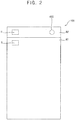
- FIG. 2 is a plan view illustrating the display panel 100 according to an embodiment.
- FIG. 2 may illustrate an example of the display panel 100 in FIG. 1 .
- the second area A2 may be located in any portion of the display panel 100 in a plan view so long as the second area A2 overlaps the functional module 400 (e.g., so long as the second area A2 overlaps the location of the functional module 400 along a direction perpendicular to the display surface).
- the functional module 400 may be disposed in any portion of the second area A2 in a plan view (e.g., so long as the functional module 400 overlaps with the second area A2 along a direction perpendicular to the display surface).
- the second area A2 may have a shape (e.g., a predetermined shape) that is substantially independent of a shape of the functional module 400 in a plan view.
- the second area A2 is located at a side of the first area A1 in a plan view and has a rectangular planar shape.
- the second area A2 may be disposed to surround the first area A1 in a plan view, or may have a polygonal planar shape.
- the functional module 400 may be disposed in various locations on the lower surface (or rear surface) of the display panel 100 within an area overlapping the second area A2 in the plan view, regardless of a shape of the functional module 400.
- FIG. 3 is a plan view illustrating the first area A1 according to an embodiment.
- FIG. 4 is a plan view illustrating the second area A2 according to an embodiment.
- FIG. 3 may illustrate an example of an area I of FIG. 2
- FIG. 4 may illustrate an example of an area II of FIG. 2 .
- the first area A1 may include a first pixel area PA1 and a first surrounding area SA1
- the second area A2 may include a second pixel area PA2, a transmission area TA, and a second surrounding area SA2.
- Each of the first pixel area PA1 and the second pixel area PA2 may be an area in which the pixels are disposed and from which light generated from each of the pixels is emitted.
- the first pixel area PA1 may include a plurality of first sub-pixel areas SRA1, SGA1, and SBA1 emitting light of different colors (e.g., different colored lights), and the second pixel area PA2 may include a plurality of second sub-pixel areas SRA2, SGA2, and SBA2 emitting light of different colors (e.g., different colored lights).
- the first sub-pixel areas SRA1, SGA1, and SBA1 may include a first red pixel area SRA1 emitting red light, a first green pixel area SGA1 emitting green light and a first blue pixel area SBA1 emitting blue light
- the second sub-pixel areas SRA2, SGA2, and SBA2 may include a second red pixel area SRA2 emitting red light, a second green pixel area SGA2 emitting green light and a second blue pixel area SBA2 emitting blue light.
- the transmission area TA may be an area that transmits external light that is incident onto the display panel 100 (e.g., incident onto the transmission area TA of the display panel 100). Because the second area A2 includes the transmission area TA transmitting the external light, the functional module 400 disposed on the lower surface (or rear surface) of the display panel 100 (or behind the display panel 100) and overlapping the second area A2 may sense or recognize an object or a user in front of the display device by detecting the external light that is passes through (or is transmitted through) the transmission area TA.
- the first surrounding area SA1 may surround the first pixel area PA1.
- the second surrounding area SA2 may surround the second pixel area PA2 and the transmission area TA.
- Each of the first surrounding area SA1 and the second surrounding area SA2 may be an area from which light is not emitted and through which the external light does not pass.
- the number of the second sub-pixel areas SRA2, SGA2, and SBA2 per a unit area may be less than the number of the first sub-pixel areas SRA1, SGA1, and SBA1 per the unit area.
- a resolution of the second area A2 may be less than a resolution of the first area A1 (e.g., the second area A2 may have a lower resolution than the first area A1 or a density of second sub-pixel areas SRA2, SGA2, and SBA2 of the second area A2 may be lower than a density of first sub-pixel areas SRA1, SGA1, and SBA1 of the first area A1).
- the number of the second sub-pixel areas SRA2, SGA2, and SBA2 per the unit area may be 1/2 (or half or 50%) of the number of the first sub-pixel areas SRA1, SGA1, and SBA1 per the unit area.
- FIGS. 3 and 4 show sixteen (16) first sub-pixel areas SRA1, SGA1, and SBA1 per unit area UA
- FIG. 4 shows eight (8) second sub-pixel areas SRA2, SGA2, and SBA2 per unit area UA (e.g., a unit area UA of the same size as the unit area UA shown in FIG. 3 ).
- the first green pixel area SGA1 may be spaced (or spaced apart) from the first red pixel area SRA1 in (or along) a first direction DR1 or a second direction DR2 perpendicular to the first direction DR1.
- the first blue pixel area SBA1 may be spaced (or spaced apart) from the first red pixel area SRA1 in (or along) a third direction DR3 between the first direction DR1 and the second direction DR2 (e.g., bisecting the first direction DR1 and the second direction DR2) or a fourth direction DR4 perpendicular to the third direction DR3.
- the third direction DR3 may form a 45 degree angle with the first direction DR1 in a clockwise direction
- the fourth direction DR4 may form a 45 degree angle with the second direction DR2 in the clockwise direction.
- an arrangement of the second sub-pixel areas SRA2, SGA2, and SBA2 may be substantially the same as an arrangement of the first sub-pixel areas SRA1, SGA1, and SBA1.
- the second green pixel area SGA2 may be spaced (or spaced apart) from the second red pixel area SRA2 in (or along) the first direction DR1 or the second direction DR2.
- the second blue pixel area SBA2 may be spaced (or spaced apart) from the second red pixel area SRA2 in the third direction DR3 or the fourth direction DR4.
- a size of each of the second sub-pixel areas SRA2, SGA2, and SBA2 may be substantially the same as a size as a respective one of each of the first sub-pixel areas SRA1, SGA1, and SBA1.
- a size of the second red pixel area SRA2, a size of the second green pixel area SGA2, and a size of the second blue pixel area SBA2 may be substantially the same as a size of the first red pixel area SRA1, a size of the first green pixel area SGA1, and a size of the first blue pixel area SBA1, respectively.
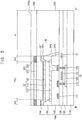
- FIG. 5 is a cross-sectional view illustrating a portion of a display device according to an embodiment.
- FIG. 5 may illustrate an example of the second area A2 taken along a line III-III' in FIG. 4 .
- FIG. 5 illustrates a cross-sectional structure of the second area A2
- a cross-sectional structure of the first area A1 may be substantially the same as the cross-sectional structure of the second area A2 except for the transmission area TA.
- a cross-sectional structure of the first pixel area PA1 and a cross-sectional structure of the first surrounding area SA1 may be substantially the same as a cross-sectional structure of the second pixel area PA2 and a cross-sectional structure of the second surrounding area SA2, respectively.
- a display device may include a display panel 100, an encapsulation structure 200, a color filter layer 300, and an overcoat layer 500.
- the display panel 100 may include a substrate 110, a plurality of conductive layers 120, 131, 132, 141, 142, and 143 (the conductive layers may include one or more semiconductor layers), a plurality of inorganic insulation layers 125 and 135, an organic insulation layer 145, a pixel electrode 150, a pixel defining layer 160, an emission layer 170, and an opposite electrode 180.
- the substrate 110 may be a transparent insulating substrate.
- the substrate 110 may be formed of glass, quartz, plastic, or the like.
- the conductive layers 120, 131, 132, 141, 142, and 143 located on different layers from each other may be disposed on the substrate 110.
- the conductive layers 120,131, 132, 141, 142, and 143 may include an active layer 120, a gate line 131, a gate electrode 132, a data line 141, a source electrode 142, and a drain electrode 143.
- the inorganic insulation layers 125 and 135 located on different layers from each other and insulating the conductive layers 120, 131, 132, 141, 142, and 143 may be disposed on the substrate 110.
- the inorganic insulation layers 125 and 135 may include a gate insulation layer 125 and an insulation interlayer 135.
- the active layer 120 may be disposed on the substrate 110.
- the active layer 120 may be formed of amorphous silicon, polysilicon, an oxide semiconductor, or the like.
- the active layer 120 may include a source region, a drain region, and a channel region disposed between the source region and the drain region.
- the source region and the drain region may be doped with P-type or N-type impurities, and the channel region may be doped with a different type of impurities from the impurities doped in the source region and the drain region (e.g., if the source and drain regions are doped with P-type impurities, then the channel region may be doped with N-type impurities; likewise, if the source and drain regions are doped with N-type impurities, then the channel region may be doped with P-type impurities).
- the gate insulation layer 125 may be disposed on the active layer 120.
- the gate insulation layer 125 may cover the active layer 120, and may be formed on the substrate 110.
- the gate insulation layer 125 may insulate the gate line 131 and the gate electrode 132 from the active layer 120.
- the gate insulation layer 125 may be formed of an inorganic insulation material such as silicon nitride, silicon oxide, silicon oxynitride, or the like.
- the gate line 131 and the gate electrode 132 may be disposed on the gate insulation layer 125.
- the gate line 131 may extend in a direction (e.g., a row direction of the display panel), and may transmit a gate signal.
- the gate electrode 132 may overlap the channel region of the active layer 120.
- the gate line 131 and the gate electrode 132 may be formed of conductive material such as metal, an alloy of the metal, or the like.
- the insulation interlayer 135 may be disposed on the gate line 131 and the gate electrode 132.
- the insulation interlayer 135 may cover the gate line 131 and the gate electrode 132, and may be formed on the gate insulation layer 125.
- the insulation interlayer 135 may insulate the data line 141, the source electrode 142, and the drain electrode 143 from the gate line 131 and the gate electrode 132.
- the insulation interlayer 135 may be formed of an inorganic insulation material such as silicon nitride, silicon oxide, silicon oxynitride, or the like.
- the data line 141, the source electrode 142, and the drain electrode 143 may be disposed on the insulation interlayer 135.
- the data line 141 may extend in a direction crossing the gate line 131 (e.g., a column direction of the display panel), and may transmit a data signal.
- the source electrode 142 may be connected to the source region of the active layer 120, and the drain electrode 143 may be connected to the drain region of the active layer 120.
- the data line 141, the source electrode 142, and the drain electrode 143 may be formed of a conductive material such as metal, an alloy of the metal, or the like.
- the active layer 120, the gate electrode 132, the source electrode 142, and the drain electrode 143 may form a transistor TR.
- the organic insulation layer 145 may be disposed on the data line 141, the source electrode 142, and the drain electrode 143.
- the organic insulation layer 145 may cover the data line 141, the source electrode 142, and the drain electrode 143, and may be formed on the insulation interlayer 135.
- the organic insulation layer 145 may protect the gate line 131, the data line 141, and the transistor TR, and may provide a planarized surface (or planar surface) thereon.
- the organic insulation layer 145 may be formed of inorganic insulation material such as polyimide (PI), or the like.
- the pixel electrode 150 may be disposed on the organic insulation layer 145.
- the pixel electrode 150 may be connected to the source electrode 142 or the drain electrode 143.
- the pixel electrode 150 of each sub-pixel may be formed to correspond to the sizes and shapes of corresponding first sub-pixel areas SRA1, SGA1, and SBA1 of the first pixel area PA1 and of corresponding second sub-pixel areas SRA2, SGA2, and SBA2 of the second pixel area PA2.
- the pixel electrode 150 may be formed of conductive material such as metal, transparent conductive oxide, or the like.
- the pixel defining layer 160 may be disposed on the pixel electrode 150.
- the pixel defining layer 160 may include a pixel opening exposing a center portion of the pixel electrode 150 thereby defining the first pixel area PA1 and the second pixel area PA2. Further, the pixel defining layer 160 may space the opposite electrode 180 from an edge of the pixel electrode 150 thereby reducing the likelihood or preventing arcing or the like from occurring between the edge of the pixel electrode 150 and the opposite electrode 180.
- the emission layer 170 may be disposed on the pixel electrode 150.
- the emission layer 170 may be disposed on the portion of the pixel electrode 150 exposed by the pixel opening (e.g., the center portion of the pixel electrode 150).
- the emission layer 170 may include at least one of organic light emitting material and quantum dot.
- the organic light emitting material may include a low molecular weight polymer or a high molecular weight polymer.
- the low molecular weight polymer may include copper phthalocyanine, N,N'-diphenylbenzidine, tris-(8-hydroxyquinoline)aluminum, etc.
- the high molecular weight polymer may include poly(3,4-ethylenedioxythiophene), polyaniline, poly-phenylenevinylene, polyfluorene, etc.
- the quantum dot may include a core that includes a group II-VI compound, a group III-V compound, a group IV-VI compound, a group IV element, a group IV compound, and a combination thereof.
- the quantum dot may have a core-shell structure that includes the core and a shell surrounding the core. The shell may serve as a protective layer for mitigating or preventing chemical degeneration of the core to maintain semiconductor properties of the core and a charging layer for imparting electrophoretic properties to the quantum dot.
- the opposite electrode 180 may be disposed on the emission layer 170.
- the opposite electrode 180 may also be disposed on the pixel defining layer 160.
- the opposite electrode 180 may be opposite to (e.g., facing or extend in a plane parallel and overlapping) the pixel electrode 150 with the emission layer 170 in between (or therebetween).
- the opposite electrode 180 may be formed of a conductive material such as metal, transparent conductive oxide, or the like.
- the pixel electrode 160, the emission layer 170, and the opposite electrode 180 may form the light emitting element LE.
- the display panel 100 may further include a functional layer 190 disposed on the opposite electrode 180.
- the functional layer 190 may increase efficiency of light emitted from the light emitting element LE, and may protect the light emitting element LE.
- a structure of the functional layer 190 will be described in more detail with reference to FIG. 6 below.
- the display panel 100 may include a transmitting window TW overlapping the transmission area TA.
- the transmitting window TW may be defined by openings of the elements of the display panel 100, where the openings overlap the transmission area TA.
- the transmitting window TW may be formed in at least one of the insulation layers, e.g., the gate insulation layer 125, the insulation interlayer 135, the organic insulation layer 145, the pixel defining layer 160, or the like, included in the display panel 100.
- At least one of the organic insulation layer 145, the pixel defining layer 160, and the opposite electrode 180 may have an opening overlapping the transmission area TA. Further, when the functional layer 190 is disposed on the opposite electrode 180, the functional layer 190 may have an opening overlapping the transmission area TA.
- the functional layer 190, the opposite electrode 180, the pixel defining layer 160, and the organic insulation layer 145 may have a first opening OP1, a second opening OP2, a third opening OP3, and a fourth opening OP4, respectively.
- the first opening OP1 of the functional layer 190, the second opening OP2 of the opposite electrode 180, the third opening OP3 of the pixel defining layer 160, and the fourth opening OP4 of the organic insulation layer 145 may form the transmitting window TW.
- the display panel 100 may include the transmitting window TW overlapping the transmission area TA, so that the number of interfaces between adjacent insulation layers in the transmission area TA may be reduced, or the size of the conductive layer disposed in the transmission area TA may be reduced versus comparative display panels. Accordingly, reflectance of external light at the interfaces between the adjacent insulation layers or by the conductive layer may decrease or be reduced in comparison to comparative display panels.
- the encapsulation structure 200 may be disposed on the display panel 100.
- the encapsulation structure 200 may include at least one inorganic layer and at least one organic layer.
- a portion of the encapsulation structure 200 which overlaps the first pixel area PA1, the first surrounding area SA1, the second pixel area PA2 and the second surrounding area SA2, may be disposed on the light emitting element LE, thereby preventing or blocking impurities from permeating into the light emitting element LE from outside and protecting the light emitting element LE from external impact. Further, a portion of the encapsulation structure 200, which overlaps the transmission area TA, may fill the transmitting window TW.
- the encapsulation structure 200 may have a planarized upper surface (or planar upper surface) throughout the first pixel area PA1, the first surrounding area SA1, the second pixel area PA2, the transmission area TA, and the second surrounding area SA2. Elements of the encapsulation structure 200 will be described in more detail with reference to FIG. 6 below.
- the color filter layer 300 may be disposed on the encapsulation structure 200.
- the color filter layer 300 may include a color filter 310 and a black matrix 320.
- the color filter 310 may overlap the first pixel area PA1 and the second pixel area PA2.
- the color filter 310 may include a red color filter, a green color filter, and a blue color filter.
- the red color filter may overlap the first red pixel area SRA1 and the second red pixel area SRA2
- the green color filter may overlap the first green pixel area SGA1 and the second green pixel area SGA2
- the blue color filter may overlap the first blue pixel area SBA1 and the second blue pixel area SBA2.
- the color filter 310 may absorb light of wavelengths except for (or other than) a wavelength (or wavelengths or a portion of a visible light spectrum) corresponding to respective color of the color filter 310 from external light. Accordingly, when light emitted from the light emitting element LE passes through the color filter 310 and is emitted to the outside, because the light does not mix with external light of another wavelength (e.g., of another color), the color filter 310 may reduce or prevent reflection of the external light and thereby increase or improve color purity of the light emitted from the light emitting element LE.
- the color filter 310 may be formed of acrylic resin, polyimide-based resin, or the like.
- the black matrix 320 may overlap the first surrounding area SA1 and the second surrounding area SA2.
- the black matrix 320 may have a black color.
- the black matrix 320 may absorb most of external light incident onto the black matrix 320. Accordingly, the black matrix 320 may reduce or prevent the reflection of external light.
- the black matrix 320 may be formed of chromium (Cr), chromium oxide (CrO x ), chromium nitride (CrN x ), carbon black, a pigment mixture, a dye mixture, or the like.
- the overcoat layer 500 may be disposed on the encapsulation structure 200.
- the overcoat layer 500 may overlap at least the transmission area TA thereby removing or planarizing a step formed by the color filter layer 300 on the encapsulation structure 200.
- the overcoat layer 500 may be formed of acrylic resin, polyimide-based resin, or the like.
- the overcoat layer 500 may cover the color filter 310 and the black matrix 320, and may have a planarized upper surface 500U. In such an embodiment, the overcoat layer 500 may overlap the first pixel area PA1, the first surrounding area SA1, the second pixel area PA2, the transmission area TA, and the second surrounding area SA2. The overcoat layer 500 may protect the color filter 310 and the black matrix 320 thereby improving reliability of the color filter 310 and the black matrix 320.
- a comparative display device may include a polarizing layer disposed on the display panel 100 to reduce or prevent the reflection of external light.
- the polarizing layer overlaps the transmission area TA, the transmittance of the transmission area TA may decrease, therefore, the transmittance of the second area A2 overlapping the functional module may decrease.
- the display device may include the color filter 310 overlapping the first pixel area PA1 and the second pixel area PA2 and the black matrix 320 overlapping the first surrounding area SA1 and the second surrounding area SA2 to reduce or prevent the reflection of external light.
- the color filter 310 and the black matrix 320 do not overlap the transmission area TA so that the transmittance of the transmission area TA may increase, therefore, the transmittance of the second area A2 overlapping the functional module may increase in comparison to the comparative display device.
- FIG. 6 is a cross-sectional view illustrating the encapsulation structure 200 according to an embodiment.
- FIG. 6 may illustrate an example of the encapsulation structure 200 in FIG. 5 .
- the encapsulation structure 200 may be disposed on the functional layer 190.
- the functional layer 190 may include a capping layer 191 and a cover layer 192 disposed on the capping layer 191.
- the capping layer 191 may increase efficiency of light emitted from the light emitting element LE through refractive index matching.
- the cover layer 192 may protect or prevent the light emitting element LE from being damaged in the following process using plasma or the like.
- the capping layer 191 may include organic material, and the cover layer 192 may include lithium fluoride (LiF).
- the encapsulation structure 200 may include a first inorganic layer 210, an organic layer 220, and an second inorganic layer 230.
- the organic layer 220 may be disposed on the first inorganic layer 210, and the second inorganic layer 230 may be disposed on the organic layer 220.
- the first inorganic layer 210 and the second inorganic layer 230 may prevent or decrease impurities such as oxygen, moisture, or the like from permeating into the light emitting element LE.
- the organic layer 220 may improve encapsulating characteristics of the encapsulation structure 200, may alleviate inner stress of the first inorganic layer 210 and the second inorganic layer 230, may mitigate the effect of defects of the first inorganic layer 210 and the second inorganic layer 230, and may provide a planarized upper surface to the second inorganic layer 230.
- a difference between a refractive index of the first inorganic layer 210 and a refractive index of the organic layer 220 and a difference between the refractive index of the organic layer 220 and a refractive index of the second inorganic layer 230 may be about 0.2 or more.
- the first inorganic layer 210 may include silicon nitride (SiN x ) or silicon oxynitride (SiO x N y ) and have the refractive index of about 1.78
- the organic layer 220 may include organic material such as epoxy-based resin, acrylic resin, polyimide-based resin, or the like and have the refractive index of about 1.53
- the second inorganic layer 230 may include silicon nitride (SiN x ) and have the refractive index of about 1.94.
- the encapsulation structure 200 may further include a first low refractive inorganic layer 240 disposed between the first inorganic layer 210 and the organic layer 220 and a second low refractive inorganic layer 250 disposed between the organic layer 220 and the second inorganic layer 230.
- a refractive index of the first low refractive inorganic layer 240 may be less than the refractive index of the first inorganic layer 210 and greater than the refractive index of the organic layer 220 (e.g., the first low refractive inorganic layer 240 may have an intermediate index of refraction between the refractive index of the first inorganic layer 210 and the organic layer 220).
- the refractive index of the first low refractive inorganic layer 240 may be about 1.66.
- the refractive index of the second low refractive inorganic layer 250 may be greater than the refractive index of the organic layer 220 and less than the refractive index of the second inorganic layer 230 (e.g., the second low refractive inorganic layer 250 may have an intermediate index of refraction between the refractive index of the second inorganic layer 230 and the organic layer 220).
- the refractive index of the second low refractive inorganic layer 250 may be about 1.71.
- Each of the first low refractive inorganic layer 240 and the second low refractive inorganic layer 250 may include silicon oxynitride (SiO x N y ).
- a ratio of oxygen and nitrogen of silicon oxynitride (SiO x N y ) included in each of the first low refractive inorganic layer 240 and the second low refractive inorganic layer 250 may be changed to control a refractive index of each of the first low refractive inorganic layer 240 and the second low refractive inorganic layer 250.
- a refractive index may increase when a ratio of nitrogen in silicon oxynitride (SiO x N y ) is relatively large, and a refractive index may decrease when a ratio of oxygen in silicon oxynitride (SiO x N y ) is relatively large.
- the first low refractive inorganic layer 240 may be disposed between the first inorganic layer 210 and the organic layer 220 and the second low refractive inorganic layer 250 may be disposed between the organic layer 220 and the second inorganic layer 230, so that a difference between refractive indexes of adjacent layers included in the encapsulation structure 200 may be less than about 0.2. Accordingly, reflectance of external light reflected at an interface between the adjacent layers may decrease compared to an encapsulation structure that did not include the first low refractive inorganic layer 240 and the second low refractive inorganic layer 250. Therefore, transmittance of a portion of the encapsulation structure 200, which overlaps the transmission area TA, may increase, and transmittance of the second area A2 that the functional module overlaps may increase.
- the encapsulation structure 200 may further include a third low refractive inorganic layer 260 disposed on the second inorganic layer 230.
- a refractive index of the third low refractive inorganic layer 260 may be less than the refractive index of the second inorganic layer 230.
- the refractive index of the third low refractive inorganic layer 260 may be about 1.71.
- the third low refractive inorganic layer 260 may include silicon oxynitride (SiO x N y ).
- An adhesive layer ADL for attaching elements of the display device disposed on the encapsulation structure 200 to an upper surface of the encapsulation structure 200 may be disposed on the encapsulation structure 200.
- the adhesive layer ADL may be a pressure sensitive adhesive (PSA), an optically clear adhesive (OCA), or the like, and a refractive index of the adhesive layer ADL may be, for example, about 1.53.
- the adhesive layer ADL which has a refractive index largely (e.g., significantly) different from that of the second inorganic layer 230, is directly disposed on the second inorganic layer 230, the reflection of external light reflected at an interface between the second inorganic layer 230 and the adhesive layer ADL may increase.
- the third low refractive inorganic layer 260 may be disposed between the second inorganic layer 230 and the adhesive layer ADL, so that reflection of external light reflected at each of an interface between the second inorganic layer 230 and the third low refractive inorganic layer 260 and an interface between the third low refractive inorganic layer 260 and the adhesive layer ADL may decrease.
- FIG. 7 is a plan view illustrating a display panel according to an embodiment.
- FIG. 7 may illustrate another example of the display panel 100 in FIG. 1 .
- the second area A2 may be located to correspond to the location of the functional module 400 in a plan view.
- the functional module 400 may be disposed to correspond to the second area A2 in a plan view.
- the second area A2 may have a shape substantially the same as a shape of the functional module 400 in a plan view.
- the functional module 400 has a circular planar shape and is disposed in the display panel 100 while being spaced apart from an edge of the display panel in a plan view as illustrated in FIG. 7
- the second area A2 may be located to correspond to the location of the functional module 400 and have a circular planar shape.
- the first area A1 may surround at least a portion of the second area A2 (in the embodiment shown in FIG. 7 , the first area A1 surrounds the entirety of the second area A2 or completely surrounds the second area A2). Accordingly, a size of the second area A2 having a relatively low resolution (e.g., compared to the first area A1) may decrease (e.g., be kept small), and a size of the first area A1 having a relatively high resolution may increase.
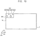
- FIGS. 8, 9 , and 10 are plan views illustrating a second area according to some embodiments.
- FIGS. 8, 9 , and 10 may illustrate other examples of the area II in FIG. 2 .
- the number of the second sub-pixel areas SRA2, SGA2, and SBA2 per the unit area may be 1/4 (one fourth), 1/9 (one ninth), or 1/16 (one sixteenth) of the number of the first sub-pixel areas SRA1, SGA1, and SBA1 per the unit area.
- the number of the second sub-pixel areas SRA2, SGA2, and SBA2 per the unit area may be 4 (as shown in FIG. 8 ).
- the number of the second sub-pixel areas SRA2, SGA2, and SBA2 per the unit area may be 4 (as shown in FIG. 9 ).
- the number of the second sub-pixel areas SRA2, SGA2, and SBA2 per the unit area may be 4 (as shown in FIG. 10 ).
- the size of the transmission area TA may increase. Accordingly, as the size of the transmission area TA increases, the transmittance of the second area A2 may increase.
- the size of the second pixel area PA2 may increase. Accordingly, as the size of the second pixel area PA2 increases, the resolution of the second area A2 may increase.
- FIGS. 11 and 12 are plan views illustrating a second area according to embodiments.
- FIGS. 11 and 12 may illustrate other examples of the area II in FIG. 2 .
- an arrangement of the second sub-pixel areas SRA2, SGA2, and SBA2 may be different from an arrangement of the first sub-pixel areas SRA1, SGA1, and SBA1.
- the second green pixel area SGA2 in the second area A2, may be spaced from the second red pixel area SRA2 in or along the third direction DR3 as illustrated in FIG. 11 .
- the second blue pixel area SBA2 may be spaced from the second green pixel area SGA2 in the third direction DR3.
- the second green pixel area SGA2 may be spaced from the second red pixel area SRA2 in the fourth direction DR4 as illustrated in FIG. 12 .
- the second blue pixel area SBA2 may be spaced from the second red pixel area SRA2 and the second green pixel area SGA2 in the third direction DR3.
- a size of each of the second sub-pixel areas SRA2, SGA2, and SBA2 may be greater than a size of each of the first sub-pixel areas SRA1, SGA1, and SBA1.
- a size of the second red pixel area SRA2, a size of the second green pixel area SGA2, and a size of the second blue pixel area SBA2 may be greater a size of the first red pixel area SRA1, a size of the first green pixel area SGA1, and a size of the first blue pixel area SBA1, respectively.
- a brightness of light emitted from the light emitting element disposed in the second pixel area PA2 may be greater than a brightness of light emitted from the light emitting element disposed in the first pixel area PA1 such that a brightness of an image displayed in the second area A2 may be substantially equal to a brightness of an image displayed in the first area A1. In this case, a lifespan of the light emitting element disposed in the second pixel area PA2 may decrease.
- each of the second sub-pixel areas SRA2, SGA2, and SBA2 is greater than the size of each of the first sub-pixel areas SRA1, SGA1, and SBA1
- the brightness of an image displayed in the second area A2 may be substantially equal to the brightness of an image displayed in the first area A1. Accordingly, a lifespan of the light emitting element disposed in the second pixel area PA2 may increase or be improved.
- FIG. 13 is a cross-sectional view illustrating a portion of a display device according to an embodiment.
- FIG. 13 may illustrate another example of the second area A2 taken along the line III-III' in FIG. 4 .
- the display device described with reference to FIG. 13 may be substantially the same as the display device described with reference to FIG. 5 except for structures of the gate insulation layer 1125 and the insulation interlayer 1135. Accordingly, descriptions on elements of the display device described with reference to FIG. 13 , which are substantially the same as or similar to those of the display device described with reference to FIG. 5 , will not be repeated in detail herein.
- At least one of the gate insulation layer 1125, the insulation interlayer 1135, the organic insulation layer 145, the pixel defining layer 160, and the opposite electrode 180 may have an opening overlapping the transmission area TA.
- the functional layer 190, the opposite electrode 180, the pixel defining layer 160, the organic insulation layer 145, the insulation interlayer 1135, and the gate insulation layer 1125 may have a first opening OP1, a second opening OP2, a third opening OP3, a fourth opening OP4, a fifth opening OP5, and a sixth opening OP6, respectively.
- the first opening OP1 of the functional layer 190, the second opening OP2 of the opposite electrode 180, the third opening OP3 of the pixel defining layer 160, the fourth opening OP4 of the organic insulation layer 145, the fifth opening OP5 of the insulation interlayer 1135, and the sixth opening OP6 of the gate insulation layer 1125 may form the transmitting window TW.
- FIG. 14 is a cross-sectional view illustrating a portion of a display device according to an embodiment.
- FIG. 14 may illustrate another example of the second area A2 taken along the line III-III' in FIG. 4 .
- the display device described with reference to FIG. 14 may be substantially the same as the display device described with reference to FIG. 13 except for a structure of the pixel defining layer 1160. Accordingly, descriptions on elements of the display device described with reference to FIG. 14 , which are substantially the same as or similar to those of the display device described with reference to FIG. 13 , will not be repeated in detail.
- the pixel defining layer 1160 may have a black color.
- the pixel defining layer 1160 may absorb most of external light incident onto the pixel defining layer 1160. Accordingly, the pixel defining layer 1160 may reduce or prevent the reflection of external light.
- the pixel defining layer 1160 may be formed of carbon black, phenylene black, aniline black, cyanine black, nigrosin acid black, black resin, or the like.
- the pixel defining layer 1160 may overlap a portion of each of the conductive layers 120, 131, 132, 141, 142, and 143, the inorganic insulation layers 1125 and 1135, and the organic insulation layer 145, which overlaps the transmission area TA.
- the pixel defining layer 1160 may overlap the portion of each of the gate line 131, the gate insulation layer 1125, the insulation interlayer 1135, and the organic insulation layer 145, which overlaps the transmission area TA.
- FIGS. 15 and 16 are cross-sectional views illustrating a portion of a display device according to embodiments.
- FIGS. 15 and 16 may illustrate other examples of the second area A2 taken along the line III-III' in FIG. 4 .
- the display device described with reference to FIGS. 15 and 16 may be substantially the same as the display device described with reference to FIG. 13 except for an addition of a shielding layer 600. Accordingly, descriptions on elements of the display device described with reference to FIGS. 15 and 16 , which are substantially the same as or similar to those of the display device described with reference to FIG. 13 , will not be repeated in detail.
- the display device may include a shielding layer 600 overlapping the first surrounding area SA1 and the second surrounding area SA2.
- the shielding layer 600 may overlap the first surrounding area SA1, the second surrounding area SA2, and an edge portion of the transmission area TA adjacent to the first surrounding area SA1 and the second surrounding area SA2.
- the shielding layer 600 may be disposed on the black matrix 320 as illustrated in FIG. 15 .
- the shielding layer 600 may cover the black matrix 320, and may be disposed on the encapsulation structure 200.
- the shielding layer 600 may be disposed between the encapsulation structure 200 and the black matrix 320 as illustrated in FIG. 16 .
- the shielding layer 600 may have a black color.
- the shielding layer 600 may absorb most of external light incident onto the shielding layer 600. Accordingly, the shielding layer 600 may reduce or prevent the reflection of external light.
- the shielding layer 600 may be formed of chromium (Cr), chromium oxide (CrO x ), chromium nitride (CrN x ), carbon black, a pigment mixture, a dye mixture, or the like.
- the shielding layer 600 may include metal.
- the shielding layer 600 may overlap a portion of each of the conductive layers 120, 131, 132, 141, 142, and 143, the inorganic insulation layers 1125 and 1135, the organic insulation layer 145, the pixel defining layer 160, and the opposite electrode 180, which overlaps the transmission area TA.
- the shielding layer 600 may overlap a portion of each of the gate line 131, the gate insulation layer 1125, the insulation interlayer 1135, the organic insulation layer 145, and the pixel defining layer 160 overlaps the transmission area TA as illustrated in FIGS.
- the shielding layer 600 may overlap the portion of each of the gate line 131, the gate insulation layer 1125, the insulation interlayer 1135, the organic insulation layer 145, and the pixel defining layer 160, which overlaps the transmission area TA. Accordingly, external light passing through the transmission area TA may not be diffracted by the portion of the conductive layers 120, 131, 132, 141, 142, and 143, the inorganic insulation layers 1125 and 1135, the organic insulation layer 145, the pixel defining layer 160, and the opposite electrode 180, which overlaps the transmission area TA, at an edge of the transmission area TA. Thus, the decrease of the transmittance of the transmission area TA may be mitigated or prevented.
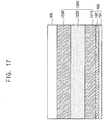
- FIG. 17 is a cross-sectional view illustrating the encapsulation structure 200 according to an embodiment.
- FIG. 17 may illustrate another example of the encapsulation structure 200 in FIG. 5 .
- the encapsulation structure 200 may be disposed on the functional layer 190.
- the encapsulation structure 200 may include a first inorganic layer 1210, an organic layer 1220, and an second inorganic layer 1230.
- the organic layer 1220 may be disposed on the first inorganic layer 1210, and the second inorganic layer 1320 may be disposed on the organic layer 1220.
- a difference between a refractive index of the first inorganic layer 1210 and a refractive index of the organic layer 1220 and a difference between the refractive index of the organic layer 1220 and a refractive index of the second inorganic layer 1230 may be about 0.2 or less.
- the first inorganic layer 1210 may include silicon oxynitride (SiO x N y ) and have the refractive index of about 1.60
- the organic layer 1220 may include organic material such as epoxy-based resin, acrylic resin, polyimide-based resin, or the like and have the refractive index of about 1.5
- the second inorganic layer 230 may include silicon oxynitride (SiO x N y ) and have the refractive index of about 1.60.
- a ratio of oxygen and nitrogen of silicon oxynitride (SiO x N y ) included in each of the first inorganic layer 1210 and the second inorganic layer 1230 may be changed to control the refractive index of each of the first inorganic layer 1210 and the second inorganic layer 1230.
- a refractive index may increase when a ratio (or proportion) of nitrogen in silicon oxynitride (SiO x N y ) is relatively large (e.g., as the proportion of nitrogen to oxygen increases), and a refractive index may decrease when a ratio (or proportion) of oxygen in silicon oxynitride (SiO x N y ) is relatively large (e.g., as the proportion of oxygen to nitrogen increases).
- the refractive indexes of the first inorganic layer 1210 and the second inorganic layer 1230 may decrease. Therefore, the difference between the refractive index of the first inorganic layer 1210 and the refractive index of the organic layer 1220 and the difference between the refractive index of the organic layer 1220 and the refractive index of the second inorganic layer 1230 may be about 0.2 or less.
- reflectance of external light reflected at each of an interface between the first inorganic layer 1210 and the organic layer 1220 and an interface between the organic layer 1220 and the second inorganic layer 1230 may decrease. Therefore, transmittance of a portion of the encapsulation structure 200, which overlaps the transmission area TA, may increase, and transmittance of the second area A2 that the functional module overlaps may increase.
- a display device comprising: a display panel having a first area and a second area, the first area comprising a first pixel area and a first surrounding area surrounding the first pixel area, and the second area comprising a second pixel area, a transmission area, and a second surrounding area surrounding the second pixel area and the transmission area; an encapsulation structure on the display panel and comprising at least one inorganic layer and at least one organic layer; a color filter on the encapsulation structure and overlapping the first pixel area and the second pixel area; a black matrix on the encapsulation structure and overlapping the first surrounding area and the second surrounding area; and a functional module on a rear surface of the display panel and overlapping the second area.
- the first pixel area may comprise a plurality of first sub-pixel areas
- the second pixel area may comprise a plurality of second sub-pixel areas
- the transmission area comprises a plurality of transmission areas.
- the first surrounding area may surround the plurality of first sub-pixel areas in the first area
- the second surrounding area may surround the plurality of second sub-pixel areas and the plurality of transmission areas in the second area.
- the black matrix may overlap the first surrounding area and the second surrounding area, and not overlap the plurality of first sub-pixel areas, the plurality of second sub-pixel areas, and the plurality of transmission areas.
- the color filter may overlap the plurality of first sub-pixel areas, and the plurality of second sub-pixel areas, and not overlap first surrounding area, the second surrounding area, and the plurality of transmission areas.
- the second display area may be located entirely within the first display area and surrounded by the first display area. According to some example embodiments, however, the second display area may be arranged such that it overlaps with, or is in contact with the non-display area. That is, according to some example embodiments, the second display area may extend at least partially outside of the first display area such that the second display area may be only partially surrounded on part of its edge or edges by the first display area.
- the functional module may be optical device may be positioned or mounted at the back of the display panel (e.g., at a side of the display panel that is opposite the display surface of the display panel), at a position corresponding to the second area.
- the second area may at least partially overlap the optical device when considered in a plan view.
- the first sub-pixel areas may emit light, and the second sub-pixel areas may emit light.
- the transmission areas may be areas that transmit external light that is incident onto the display panel.
- the first sub-pixel areas may be arranged in a matrix in the first area, and the second sub-pixel areas and transmissive areas may be arranged in a corresponding matrix (e.g. with the same pitch) in the second area.
- the first sub-pixel areas may be arranged in rows and columns, and in the second area, the second first sub-pixel areas and transmissive areas may be arranged in corresponding rows and columns.
- the second sub-pixel areas and transmissive areas may be arranged in various ways.
- the second sub-pixel areas and transmissive areas may be arranged alternately in a checkerboard pattern.
- the first sub-pixel areas and second sub-pixel areas may each include a respective pixel circuit.
- the display device may be applied to a display device included in a computer, a notebook, a mobile phone, a smartphone, a smart pad, a PMP, a PDA, an MP3 player, or the like.
Landscapes
- Physics & Mathematics (AREA)
- Engineering & Computer Science (AREA)
- Microelectronics & Electronic Packaging (AREA)
- Optics & Photonics (AREA)
- Geometry (AREA)
- Chemical & Material Sciences (AREA)
- Inorganic Chemistry (AREA)
- Electroluminescent Light Sources (AREA)
- Devices For Indicating Variable Information By Combining Individual Elements (AREA)
- Optical Filters (AREA)
Abstract
Description
- Embodiments relate to a display device. More particularly, embodiments relate to a display device including a functional module.
- A display device may display images based on electrical signals, and may provide users visual information. The display device may include a transmission area, and external light incident onto the display device passes through the transmission area. A functional module such as a camera module, a sensor module, etc. disposed on a rear surface of the display device may sense or recognize objects, users, etc. that are located in front of the display device through the transmission area.
- The display device may include wirings, electrodes, etc. including metal, so that external light incident onto the display device may be reflected by the wirings, electrodes, etc. To reduce or prevent the reflection of the external light, the display device may include a polarizing layer. Although the polarizing layer may reduce or prevent the reflection of the external light, however, the transmittance in the transmission area of the display device may be degraded due to the polarizing layer.
- Embodiments provide a display device having reduced external light reflectance and improved transmittance in a transmission area.
- A display device according to embodiments may include a display panel having a first area and a second area, the first area including a first pixel area and a first surrounding area surrounding the first pixel area, and the second area including a second pixel area, a transmission area, and a second surrounding area surrounding the second pixel area and the transmission area, an encapsulation structure on the display panel and including at least one inorganic layer and at least one organic layer, a color filter on the encapsulation structure and overlapping the first pixel area and the second pixel area, a black matrix on the encapsulation structure and overlapping the first surrounding area and the second surrounding area, and a functional module on a rear surface of the display panel and overlapping the second area.
- In an embodiment, the first pixel area may include a plurality of first sub-pixel areas, the second pixel area may include a plurality of second sub-pixel areas, and a number of the second sub-pixel areas per a unit area may be less than a number of the first sub-pixel areas per the unit area.
- In an embodiment, the number of the second sub-pixel areas per the unit area may be 1/2, 1/4, 1/9, or 1/16 of the number of the first sub-pixel areas per the unit area.
- In an embodiment, an arrangement of the second sub-pixel areas may be different from an arrangement of the first sub-pixel areas.
- In an embodiment, a size of each of the second sub-pixel areas may be greater than a size of each of the first sub-pixel areas.
- In an embodiment, the first area may surround at least a portion of the second area.
- In an embodiment, the display device may further include an overcoat layer on the encapsulation structure and overlapping at least the transmission area.
- In an embodiment, the overcoat layer may cover the color filter and the black matrix, and may have a planarized upper surface.
- In an embodiment, the display panel may include a substrate, a plurality of conductive layers at a plurality of different layers from each other on the substrate, an organic insulation layer on the conductive layers, a pixel electrode on the organic insulation layer, a pixel defining layer on the pixel electrode and defining the first pixel area and the second pixel area, an emission layer on the pixel electrode, and an opposite electrode on the emission layer and the pixel defining layer. At least one of the organic insulation layer, the pixel defining layer, and the opposite electrode may have an opening overlapping the transmission area.
- In an embodiment, the pixel defining layer may have a black color.
- In an embodiment, the display panel may further include a plurality of inorganic insulation layers at a plurality of different layers from each other on the substrate and insulating the conductive layers. At least one of the inorganic insulation layers may have an opening overlapping the transmission area.
- In an embodiment, the pixel defining layer may overlap a portion of each of the conductive layers, the inorganic insulation layers, and the organic insulation layer that overlap the transmission area.
- In an embodiment, the display device may further include a shielding layer overlapping at least the first surrounding area and the second surrounding area.
- In an embodiment, the shielding layer may be on the black matrix.
- In an embodiment, the shielding layer may be between the encapsulation structure and the black matrix.
- In an embodiment, the shielding layer may overlap a portion of each of the conductive layers, the inorganic insulation layers, the organic insulation layer, the pixel defining layer, and the opposite electrode that overlap the transmission area.
- In an embodiment, the encapsulation structure may include a first inorganic layer, an organic layer on the first inorganic layer, and a second inorganic layer on the organic layer.
- In an embodiment, the encapsulation structure may further include a first low refractive inorganic layer between the first inorganic layer and the organic layer, the low refractive inorganic layer having a refractive index less than a refractive index of the first inorganic layer and greater than a refractive index of the organic layer, and a second low refractive inorganic layer between the organic layer and the first inorganic layer and having a refractive index greater than the refractive index of the organic layer and less than a refractive index of the second inorganic layer.
- In an embodiment, each of the first low refractive inorganic layer and the second low refractive inorganic layer may include silicon oxynitride.
- In an embodiment, the encapsulation structure may further include a low refractive inorganic layer on the second inorganic layer and having a refractive index less than a refractive index of the second inorganic layer.
- In an embodiment, the low refractive inorganic layer may include silicon oxynitride.
- In an embodiment, each of a difference between a refractive index of the first inorganic layer and a refractive index of the organic layer and a difference between the refractive index of the organic layer and a refractive index of the second inorganic layer may be less than about 0.2.
- In an embodiment, each of the first inorganic layer and the second inorganic layer may include silicon oxynitride.
- In an embodiment, the functional module may include at least one of a camera module, a face recognition sensor module, a pupil recognition sensor module, an acceleration sensor module, a proximity sensor module, an infrared sensor module, and an ambient light sensor module.
- A display device according to embodiments may include a display panel having a first area and a second area, the first area including a first pixel area and a first surrounding area surrounding the first pixel area, and the second area including a second pixel area, a transmission area and a second surrounding area surrounding the second pixel area and the transmission area, an encapsulation structure on the display panel and including at least one inorganic layer and at least one organic layer, a color filter on the encapsulation structure and overlapping the first pixel area and the second pixel area, and a black matrix on the encapsulation structure and overlapping the first surrounding area and the second surrounding area. The display panel may include a transmitting window formed in at least one of a plurality of insulation layers included in the display panel and overlapping the transmission area.
- The display device according to embodiments may include the color filter on the encapsulation structure and overlapping the first and second pixel areas of the display panel and the black matrix on the encapsulation structure and overlapping the first and second surrounding areas of the display panel, and the display panel may include the transmitting window overlapping the transmission area. Accordingly, a polarizing layer may be omitted, and thus, the transmittance of the transmission area may increase and the reflection of external light may be prevented.
- According to an aspect, there is provided a display device as set out in claim 1. Additional features are set out in claims 2 to 14.
- According to an aspect, there is provided a display device as set out in claim 15.
- The accompanying drawings, together with the specification, illustrate exemplary embodiments of the present invention, and, together with the description, serve to explain the principles of the present invention.
-
FIG. 1 is a cross-sectional view illustrating a display device according to an embodiment. -
FIG. 2 is a plan view illustrating a display panel according to an embodiment. -
FIG. 3 is a plan view illustrating a first area according to an embodiment. -
FIG. 4 is a plan view illustrating a second area according to an embodiment. -
FIG. 5 is a cross-sectional view illustrating a portion of a display device according to an embodiment. -
FIG. 6 is a cross-sectional view illustrating an encapsulation structure according to an embodiment. -
FIG. 7 is a plan view illustrating a display panel according to an embodiment. -
FIGS. 8, 9 , and10 are plan views illustrating a second area according to embodiments. -
FIGS. 11 and 12 are plan views illustrating a second area according to embodiments. -
FIG. 13 is a cross-sectional view illustrating a portion of a display device according to an embodiment. -
FIG. 14 is a cross-sectional view illustrating a portion of a display device according to an embodiment. -
FIGS. 15 and16 are cross-sectional views illustrating a portion of a display device according to embodiments. -
FIG. 17 is a cross-sectional view illustrating an encapsulation structure according to an embodiment. - Hereinafter, display devices in accordance with embodiments will be explained in detail with reference to the accompanying drawings, in which like reference numbers refer to like elements throughout. The present invention, however, may be embodied in various different forms, and should not be construed as being limited to only the illustrated embodiments herein. Rather, these embodiments are provided as examples so that this disclosure will be thorough and complete, and will fully convey the aspects and features of the present invention to those skilled in the art. Accordingly, processes, elements, and techniques that are not necessary to those having ordinary skill in the art for a complete understanding of the aspects and features of the present invention may not be described. Unless otherwise noted, like reference numerals denote like elements throughout the attached drawings and the written description, and thus, descriptions thereof will not be repeated. In the drawings, the relative sizes of elements, layers, and regions may be exaggerated for clarity.
- It will be understood that, although the terms "first," "second," "third," etc., may be used herein to describe various elements, components, regions, layers and/or sections, these elements, components, regions, layers and/or sections should not be limited by these terms. These terms are used to distinguish one element, component, region, layer or section from another element, component, region, layer or section. Thus, a first element, component, region, layer or section described below could be termed a second element, component, region, layer or section, without departing from the scope of the present invention.
- Spatially relative terms, such as "beneath," "below," "lower," "under," "above," "upper," and the like, may be used herein for ease of explanation to describe one element or feature's relationship to another element(s) or feature(s) as illustrated in the figures. It will be understood that the spatially relative terms are intended to encompass different orientations of the device in use or in operation, in addition to the orientation depicted in the figures. For example, if the device in the figures is turned over, elements described as "below" or "beneath" or "under" other elements or features would then be oriented "above" the other elements or features. Thus, the example terms "below" and "under" can encompass both an orientation of above and below. The device may be otherwise oriented (e.g., rotated 90 degrees or at other orientations) and the spatially relative descriptors used herein should be interpreted accordingly.
- As used herein, when two elements or components that are both disposed on the same substrate "overlap," the two elements or components are, respectively, above and below one another and arranged such that a line perpendicular to the substrate passes through both elements.
- It will be understood that when an element or layer is referred to as being "on," "connected to," or "coupled to" another element or layer, it can be directly on, connected to, or coupled to the other element or layer, or one or more intervening elements or layers may be present. In addition, it will also be understood that when an element or layer is referred to as being "between" two elements or layers, it can be the only element or layer between the two elements or layers, or one or more intervening elements or layers may also be present.
- The terminology used herein is for the purpose of describing particular embodiments only and is not intended to be limiting of the present invention. As used herein, the singular forms "a" and "an" are intended to include the plural forms as well, unless the context clearly indicates otherwise. It will be further understood that the terms "comprises," "comprising," "includes," and "including," when used in this specification, specify the presence of the stated features, integers, steps, operations, elements, and/or components, but do not preclude the presence or addition of one or more other features, integers, steps, operations, elements, components, and/or groups thereof. As used herein, the term "and/or" includes any and all combinations of one or more of the associated listed items. Expressions such as "at least one of," when preceding a list of elements, modify the entire list of elements and do not modify the individual elements of the list.
- As used herein, the term "substantially," "about," and similar terms are used as terms of approximation and not as terms of degree, and are intended to account for the inherent deviations in measured or calculated values that would be recognized by those of ordinary skill in the art. Further, the use of "may" when describing embodiments of the present invention refers to "one or more embodiments of the present invention." As used herein, the terms "use," "using," and "used" may be considered synonymous with the terms "utilize," "utilizing," and "utilized," respectively. Also, the term "exemplary" is intended to refer to an example or illustration.
- Unless otherwise defined, all terms (including technical and scientific terms) used herein have the same meaning as commonly understood by one of ordinary skill in the art to which the present invention belongs. It will be further understood that terms, such as those defined in commonly used dictionaries, should be interpreted as having a meaning that is consistent with their meaning in the context of the relevant art and/or the present specification, and should not be interpreted in an idealized or overly formal sense, unless expressly so defined herein.
-
FIG. 1 is a cross-sectional view illustrating a display device according to an embodiment. - Referring to
FIG. 1 , a display device may include adisplay panel 100, anencapsulation structure 200, acolor filter layer 300, a window WM, and afunctional module 400. - The
display panel 100 may have a first area A1 and a second area A2. Each of the first area A1 and the second area A2 may be a display area for displaying an image. The second area A2 may include a transmission area transmitting external light. Accordingly, the second area A2 may transmit the external light incident onto the second area A2, and may also display the image. The first area A1 and the second area A2 may be located to be adjacent to each other. - The
encapsulation structure 200 may be disposed on thedisplay panel 100. Theencapsulation structure 200 may block or prevent impurities such as oxygen, moisture, etc. from permeating into a light emitting element included in thedisplay panel 100. Further, theencapsulation structure 200 may protect the light emitting element from external impact. - The
color filter layer 300 may be disposed on theencapsulation structure 200. Thecolor filter layer 300 may reduce or prevent the reflection of external light incident onto the display device. Further, thecolor filter layer 300 may transmit light generated from thedisplay panel 100, and may improve a purity of the color of the image displayed by the display device. - The window WM may be disposed on the
color filter layer 300. The window WM may protect elements of the display device, and may provide a display surface (or front surface) through which the image formed from thedisplay panel 100 is displayed. - The
functional module 400 may be disposed on a lower surface (or rear surface) 100L of thedisplay panel 100. Thefunctional module 400 may include, for example, a camera module for taking a photo of (or recognizing) an image of an object located in front of the display device, a face recognition sensor module for sensing a face of a user, a pupil recognition sensor module for sensing pupils of a user, an acceleration sensor module for determining a movement of the display device, a proximity sensor module and an infrared sensor module for detecting proximity of objects to a front surface of the display device, an ambient light sensor module for measuring external brightness, or the like. - The
functional module 400 may overlap the second area A2 of thedisplay panel 100. The second area A2 may include the transmission area as described above, so that thefunctional module 400 disposed on the lower surface (or rear surface) 100L of the display panel 100 (or behind the display panel 100) may sense or recognize an object or a user in front of the display device (or in front of the display panel, e.g., facing a front surface or upper surface of the display panel) through the transmission area included in the second area A2 of thedisplay panel 100. -
FIG. 2 is a plan view illustrating thedisplay panel 100 according to an embodiment.FIG. 2 may illustrate an example of thedisplay panel 100 inFIG. 1 . - Referring to
FIG. 2 , in an embodiment, the second area A2 may be located in any portion of thedisplay panel 100 in a plan view so long as the second area A2 overlaps the functional module 400 (e.g., so long as the second area A2 overlaps the location of thefunctional module 400 along a direction perpendicular to the display surface). In other words, thefunctional module 400 may be disposed in any portion of the second area A2 in a plan view (e.g., so long as thefunctional module 400 overlaps with the second area A2 along a direction perpendicular to the display surface). Further, the second area A2 may have a shape (e.g., a predetermined shape) that is substantially independent of a shape of thefunctional module 400 in a plan view.FIG. 2 illustrates that the second area A2 is located at a side of the first area A1 in a plan view and has a rectangular planar shape. However, embodiments of the present disclosure are not limited thereto, and the second area A2 may be disposed to surround the first area A1 in a plan view, or may have a polygonal planar shape. Accordingly, thefunctional module 400 may be disposed in various locations on the lower surface (or rear surface) of thedisplay panel 100 within an area overlapping the second area A2 in the plan view, regardless of a shape of thefunctional module 400. -
FIG. 3 is a plan view illustrating the first area A1 according to an embodiment.FIG. 4 is a plan view illustrating the second area A2 according to an embodiment.FIG. 3 may illustrate an example of an area I ofFIG. 2 , andFIG. 4 may illustrate an example of an area II ofFIG. 2 . - Referring to
FIGS. 3 and 4 , the first area A1 may include a first pixel area PA1 and a first surrounding area SA1, and the second area A2 may include a second pixel area PA2, a transmission area TA, and a second surrounding area SA2. Each of the first pixel area PA1 and the second pixel area PA2 may be an area in which the pixels are disposed and from which light generated from each of the pixels is emitted. - The first pixel area PA1 may include a plurality of first sub-pixel areas SRA1, SGA1, and SBA1 emitting light of different colors (e.g., different colored lights), and the second pixel area PA2 may include a plurality of second sub-pixel areas SRA2, SGA2, and SBA2 emitting light of different colors (e.g., different colored lights). In an embodiment, the first sub-pixel areas SRA1, SGA1, and SBA1 may include a first red pixel area SRA1 emitting red light, a first green pixel area SGA1 emitting green light and a first blue pixel area SBA1 emitting blue light, and the second sub-pixel areas SRA2, SGA2, and SBA2 may include a second red pixel area SRA2 emitting red light, a second green pixel area SGA2 emitting green light and a second blue pixel area SBA2 emitting blue light.
- The transmission area TA may be an area that transmits external light that is incident onto the display panel 100 (e.g., incident onto the transmission area TA of the display panel 100). Because the second area A2 includes the transmission area TA transmitting the external light, the
functional module 400 disposed on the lower surface (or rear surface) of the display panel 100 (or behind the display panel 100) and overlapping the second area A2 may sense or recognize an object or a user in front of the display device by detecting the external light that is passes through (or is transmitted through) the transmission area TA. The first surrounding area SA1 may surround the first pixel area PA1. The second surrounding area SA2 may surround the second pixel area PA2 and the transmission area TA. Each of the first surrounding area SA1 and the second surrounding area SA2 may be an area from which light is not emitted and through which the external light does not pass. - Because the second area A2 includes the transmission area TA, the number of the second sub-pixel areas SRA2, SGA2, and SBA2 per a unit area may be less than the number of the first sub-pixel areas SRA1, SGA1, and SBA1 per the unit area. In other words, a resolution of the second area A2 may be less than a resolution of the first area A1 (e.g., the second area A2 may have a lower resolution than the first area A1 or a density of second sub-pixel areas SRA2, SGA2, and SBA2 of the second area A2 may be lower than a density of first sub-pixel areas SRA1, SGA1, and SBA1 of the first area A1).
- In an embodiment, the number of the second sub-pixel areas SRA2, SGA2, and SBA2 per the unit area may be 1/2 (or half or 50%) of the number of the first sub-pixel areas SRA1, SGA1, and SBA1 per the unit area. For example, as illustrated in
FIGS. 3 and 4, FIG. 3 shows sixteen (16) first sub-pixel areas SRA1, SGA1, and SBA1 per unit area UA, andFIG. 4 shows eight (8) second sub-pixel areas SRA2, SGA2, and SBA2 per unit area UA (e.g., a unit area UA of the same size as the unit area UA shown inFIG. 3 ). - In the first area A1, the first green pixel area SGA1 may be spaced (or spaced apart) from the first red pixel area SRA1 in (or along) a first direction DR1 or a second direction DR2 perpendicular to the first direction DR1. Further, the first blue pixel area SBA1 may be spaced (or spaced apart) from the first red pixel area SRA1 in (or along) a third direction DR3 between the first direction DR1 and the second direction DR2 (e.g., bisecting the first direction DR1 and the second direction DR2) or a fourth direction DR4 perpendicular to the third direction DR3. For example, the third direction DR3 may form a 45 degree angle with the first direction DR1 in a clockwise direction, and the fourth direction DR4 may form a 45 degree angle with the second direction DR2 in the clockwise direction.
- In an embodiment, an arrangement of the second sub-pixel areas SRA2, SGA2, and SBA2 may be substantially the same as an arrangement of the first sub-pixel areas SRA1, SGA1, and SBA1. In such an embodiment, in the second area A2, the second green pixel area SGA2 may be spaced (or spaced apart) from the second red pixel area SRA2 in (or along) the first direction DR1 or the second direction DR2. Further, the second blue pixel area SBA2 may be spaced (or spaced apart) from the second red pixel area SRA2 in the third direction DR3 or the fourth direction DR4.
- In an embodiment, a size of each of the second sub-pixel areas SRA2, SGA2, and SBA2 may be substantially the same as a size as a respective one of each of the first sub-pixel areas SRA1, SGA1, and SBA1. For example, a size of the second red pixel area SRA2, a size of the second green pixel area SGA2, and a size of the second blue pixel area SBA2 may be substantially the same as a size of the first red pixel area SRA1, a size of the first green pixel area SGA1, and a size of the first blue pixel area SBA1, respectively.
-
FIG. 5 is a cross-sectional view illustrating a portion of a display device according to an embodiment.FIG. 5 may illustrate an example of the second area A2 taken along a line III-III' inFIG. 4 . - While
FIG. 5 illustrates a cross-sectional structure of the second area A2, a cross-sectional structure of the first area A1 may be substantially the same as the cross-sectional structure of the second area A2 except for the transmission area TA. In other words, a cross-sectional structure of the first pixel area PA1 and a cross-sectional structure of the first surrounding area SA1 may be substantially the same as a cross-sectional structure of the second pixel area PA2 and a cross-sectional structure of the second surrounding area SA2, respectively. - Referring to
FIG. 5 , a display device may include adisplay panel 100, anencapsulation structure 200, acolor filter layer 300, and anovercoat layer 500. Thedisplay panel 100 may include asubstrate 110, a plurality ofconductive layers organic insulation layer 145, apixel electrode 150, apixel defining layer 160, anemission layer 170, and anopposite electrode 180. - The
substrate 110 may be a transparent insulating substrate. For example, thesubstrate 110 may be formed of glass, quartz, plastic, or the like. - The
conductive layers substrate 110. The conductive layers 120,131, 132, 141, 142, and 143 may include anactive layer 120, agate line 131, agate electrode 132, adata line 141, asource electrode 142, and adrain electrode 143. Further, the inorganic insulation layers 125 and 135 located on different layers from each other and insulating theconductive layers substrate 110. The inorganic insulation layers 125 and 135 may include agate insulation layer 125 and aninsulation interlayer 135. - The
active layer 120 may be disposed on thesubstrate 110. Theactive layer 120 may be formed of amorphous silicon, polysilicon, an oxide semiconductor, or the like. Theactive layer 120 may include a source region, a drain region, and a channel region disposed between the source region and the drain region. The source region and the drain region may be doped with P-type or N-type impurities, and the channel region may be doped with a different type of impurities from the impurities doped in the source region and the drain region (e.g., if the source and drain regions are doped with P-type impurities, then the channel region may be doped with N-type impurities; likewise, if the source and drain regions are doped with N-type impurities, then the channel region may be doped with P-type impurities). - The
gate insulation layer 125 may be disposed on theactive layer 120. Thegate insulation layer 125 may cover theactive layer 120, and may be formed on thesubstrate 110. Thegate insulation layer 125 may insulate thegate line 131 and thegate electrode 132 from theactive layer 120. Thegate insulation layer 125 may be formed of an inorganic insulation material such as silicon nitride, silicon oxide, silicon oxynitride, or the like. - The
gate line 131 and thegate electrode 132 may be disposed on thegate insulation layer 125. Thegate line 131 may extend in a direction (e.g., a row direction of the display panel), and may transmit a gate signal. Thegate electrode 132 may overlap the channel region of theactive layer 120. Thegate line 131 and thegate electrode 132 may be formed of conductive material such as metal, an alloy of the metal, or the like. - The
insulation interlayer 135 may be disposed on thegate line 131 and thegate electrode 132. Theinsulation interlayer 135 may cover thegate line 131 and thegate electrode 132, and may be formed on thegate insulation layer 125. Theinsulation interlayer 135 may insulate thedata line 141, thesource electrode 142, and thedrain electrode 143 from thegate line 131 and thegate electrode 132. Theinsulation interlayer 135 may be formed of an inorganic insulation material such as silicon nitride, silicon oxide, silicon oxynitride, or the like. - The
data line 141, thesource electrode 142, and thedrain electrode 143 may be disposed on theinsulation interlayer 135. Thedata line 141 may extend in a direction crossing the gate line 131 (e.g., a column direction of the display panel), and may transmit a data signal. Thesource electrode 142 may be connected to the source region of theactive layer 120, and thedrain electrode 143 may be connected to the drain region of theactive layer 120. Thedata line 141, thesource electrode 142, and thedrain electrode 143 may be formed of a conductive material such as metal, an alloy of the metal, or the like. Theactive layer 120, thegate electrode 132, thesource electrode 142, and thedrain electrode 143 may form a transistor TR. - The
organic insulation layer 145 may be disposed on thedata line 141, thesource electrode 142, and thedrain electrode 143. Theorganic insulation layer 145 may cover thedata line 141, thesource electrode 142, and thedrain electrode 143, and may be formed on theinsulation interlayer 135. Theorganic insulation layer 145 may protect thegate line 131, thedata line 141, and the transistor TR, and may provide a planarized surface (or planar surface) thereon. Theorganic insulation layer 145 may be formed of inorganic insulation material such as polyimide (PI), or the like. - The
pixel electrode 150 may be disposed on theorganic insulation layer 145. Thepixel electrode 150 may be connected to thesource electrode 142 or thedrain electrode 143. Thepixel electrode 150 of each sub-pixel may be formed to correspond to the sizes and shapes of corresponding first sub-pixel areas SRA1, SGA1, and SBA1 of the first pixel area PA1 and of corresponding second sub-pixel areas SRA2, SGA2, and SBA2 of the second pixel area PA2. Thepixel electrode 150 may be formed of conductive material such as metal, transparent conductive oxide, or the like. - The
pixel defining layer 160 may be disposed on thepixel electrode 150. Thepixel defining layer 160 may include a pixel opening exposing a center portion of thepixel electrode 150 thereby defining the first pixel area PA1 and the second pixel area PA2. Further, thepixel defining layer 160 may space theopposite electrode 180 from an edge of thepixel electrode 150 thereby reducing the likelihood or preventing arcing or the like from occurring between the edge of thepixel electrode 150 and theopposite electrode 180. - The
emission layer 170 may be disposed on thepixel electrode 150. Theemission layer 170 may be disposed on the portion of thepixel electrode 150 exposed by the pixel opening (e.g., the center portion of the pixel electrode 150). Theemission layer 170 may include at least one of organic light emitting material and quantum dot. - In an embodiment, the organic light emitting material may include a low molecular weight polymer or a high molecular weight polymer. For example, the low molecular weight polymer may include copper phthalocyanine, N,N'-diphenylbenzidine, tris-(8-hydroxyquinoline)aluminum, etc., and the high molecular weight polymer may include poly(3,4-ethylenedioxythiophene), polyaniline, poly-phenylenevinylene, polyfluorene, etc.
- In an embodiment, the quantum dot may include a core that includes a group II-VI compound, a group III-V compound, a group IV-VI compound, a group IV element, a group IV compound, and a combination thereof. In an embodiment, the quantum dot may have a core-shell structure that includes the core and a shell surrounding the core. The shell may serve as a protective layer for mitigating or preventing chemical degeneration of the core to maintain semiconductor properties of the core and a charging layer for imparting electrophoretic properties to the quantum dot.
- The
opposite electrode 180 may be disposed on theemission layer 170. Theopposite electrode 180 may also be disposed on thepixel defining layer 160. Theopposite electrode 180 may be opposite to (e.g., facing or extend in a plane parallel and overlapping) thepixel electrode 150 with theemission layer 170 in between (or therebetween). Theopposite electrode 180 may be formed of a conductive material such as metal, transparent conductive oxide, or the like. Thepixel electrode 160, theemission layer 170, and theopposite electrode 180 may form the light emitting element LE. - In an embodiment, the
display panel 100 may further include afunctional layer 190 disposed on theopposite electrode 180. Thefunctional layer 190 may increase efficiency of light emitted from the light emitting element LE, and may protect the light emitting element LE. A structure of thefunctional layer 190 will be described in more detail with reference toFIG. 6 below. - The
display panel 100 may include a transmitting window TW overlapping the transmission area TA. The transmitting window TW may be defined by openings of the elements of thedisplay panel 100, where the openings overlap the transmission area TA. In an embodiment, the transmitting window TW may be formed in at least one of the insulation layers, e.g., thegate insulation layer 125, theinsulation interlayer 135, theorganic insulation layer 145, thepixel defining layer 160, or the like, included in thedisplay panel 100. - At least one of the
organic insulation layer 145, thepixel defining layer 160, and theopposite electrode 180 may have an opening overlapping the transmission area TA. Further, when thefunctional layer 190 is disposed on theopposite electrode 180, thefunctional layer 190 may have an opening overlapping the transmission area TA. - In an embodiment, the
functional layer 190, theopposite electrode 180, thepixel defining layer 160, and theorganic insulation layer 145 may have a first opening OP1, a second opening OP2, a third opening OP3, and a fourth opening OP4, respectively. In such an embodiment, the first opening OP1 of thefunctional layer 190, the second opening OP2 of theopposite electrode 180, the third opening OP3 of thepixel defining layer 160, and the fourth opening OP4 of theorganic insulation layer 145 may form the transmitting window TW. - When insulation layers are stacked in the transmission area TA, reflectance of external light reflected at interfaces between adjacent insulation layers may increase. Further, when a conductive layer is disposed in the transmission area TA, external light reflected by the conductive layer may increase the reflectance of the transmission area TA. However, the
display panel 100 according to one embodiment may include the transmitting window TW overlapping the transmission area TA, so that the number of interfaces between adjacent insulation layers in the transmission area TA may be reduced, or the size of the conductive layer disposed in the transmission area TA may be reduced versus comparative display panels. Accordingly, reflectance of external light at the interfaces between the adjacent insulation layers or by the conductive layer may decrease or be reduced in comparison to comparative display panels. - The
encapsulation structure 200 may be disposed on thedisplay panel 100. Theencapsulation structure 200 may include at least one inorganic layer and at least one organic layer. - A portion of the
encapsulation structure 200, which overlaps the first pixel area PA1, the first surrounding area SA1, the second pixel area PA2 and the second surrounding area SA2, may be disposed on the light emitting element LE, thereby preventing or blocking impurities from permeating into the light emitting element LE from outside and protecting the light emitting element LE from external impact. Further, a portion of theencapsulation structure 200, which overlaps the transmission area TA, may fill the transmitting window TW. Theencapsulation structure 200 may have a planarized upper surface (or planar upper surface) throughout the first pixel area PA1, the first surrounding area SA1, the second pixel area PA2, the transmission area TA, and the second surrounding area SA2. Elements of theencapsulation structure 200 will be described in more detail with reference toFIG. 6 below. - The
color filter layer 300 may be disposed on theencapsulation structure 200. Thecolor filter layer 300 may include acolor filter 310 and ablack matrix 320. - The
color filter 310 may overlap the first pixel area PA1 and the second pixel area PA2. Thecolor filter 310 may include a red color filter, a green color filter, and a blue color filter. The red color filter may overlap the first red pixel area SRA1 and the second red pixel area SRA2, the green color filter may overlap the first green pixel area SGA1 and the second green pixel area SGA2, and the blue color filter may overlap the first blue pixel area SBA1 and the second blue pixel area SBA2. - The
color filter 310 may absorb light of wavelengths except for (or other than) a wavelength (or wavelengths or a portion of a visible light spectrum) corresponding to respective color of thecolor filter 310 from external light. Accordingly, when light emitted from the light emitting element LE passes through thecolor filter 310 and is emitted to the outside, because the light does not mix with external light of another wavelength (e.g., of another color), thecolor filter 310 may reduce or prevent reflection of the external light and thereby increase or improve color purity of the light emitted from the light emitting element LE. Thecolor filter 310 may be formed of acrylic resin, polyimide-based resin, or the like. - The
black matrix 320 may overlap the first surrounding area SA1 and the second surrounding area SA2. Theblack matrix 320 may have a black color. Theblack matrix 320 may absorb most of external light incident onto theblack matrix 320. Accordingly, theblack matrix 320 may reduce or prevent the reflection of external light. Theblack matrix 320 may be formed of chromium (Cr), chromium oxide (CrOx), chromium nitride (CrNx), carbon black, a pigment mixture, a dye mixture, or the like. - The
overcoat layer 500 may be disposed on theencapsulation structure 200. Theovercoat layer 500 may overlap at least the transmission area TA thereby removing or planarizing a step formed by thecolor filter layer 300 on theencapsulation structure 200. Theovercoat layer 500 may be formed of acrylic resin, polyimide-based resin, or the like. - In an embodiment, the
overcoat layer 500 may cover thecolor filter 310 and theblack matrix 320, and may have a planarizedupper surface 500U. In such an embodiment, theovercoat layer 500 may overlap the first pixel area PA1, the first surrounding area SA1, the second pixel area PA2, the transmission area TA, and the second surrounding area SA2. Theovercoat layer 500 may protect thecolor filter 310 and theblack matrix 320 thereby improving reliability of thecolor filter 310 and theblack matrix 320. - A comparative display device may include a polarizing layer disposed on the
display panel 100 to reduce or prevent the reflection of external light. When the polarizing layer overlaps the transmission area TA, the transmittance of the transmission area TA may decrease, therefore, the transmittance of the second area A2 overlapping the functional module may decrease. However, the display device according to one embodiment may include thecolor filter 310 overlapping the first pixel area PA1 and the second pixel area PA2 and theblack matrix 320 overlapping the first surrounding area SA1 and the second surrounding area SA2 to reduce or prevent the reflection of external light. In some embodiments, thecolor filter 310 and theblack matrix 320 do not overlap the transmission area TA so that the transmittance of the transmission area TA may increase, therefore, the transmittance of the second area A2 overlapping the functional module may increase in comparison to the comparative display device. -
FIG. 6 is a cross-sectional view illustrating theencapsulation structure 200 according to an embodiment.FIG. 6 may illustrate an example of theencapsulation structure 200 inFIG. 5 . - Referring to
FIGS. 5 and6 , theencapsulation structure 200 may be disposed on thefunctional layer 190. Thefunctional layer 190 may include acapping layer 191 and acover layer 192 disposed on thecapping layer 191. Thecapping layer 191 may increase efficiency of light emitted from the light emitting element LE through refractive index matching. Thecover layer 192 may protect or prevent the light emitting element LE from being damaged in the following process using plasma or the like. Thecapping layer 191 may include organic material, and thecover layer 192 may include lithium fluoride (LiF). - The
encapsulation structure 200 may include a firstinorganic layer 210, anorganic layer 220, and an secondinorganic layer 230. Theorganic layer 220 may be disposed on the firstinorganic layer 210, and the secondinorganic layer 230 may be disposed on theorganic layer 220. - The first
inorganic layer 210 and the secondinorganic layer 230 may prevent or decrease impurities such as oxygen, moisture, or the like from permeating into the light emitting element LE. Theorganic layer 220 may improve encapsulating characteristics of theencapsulation structure 200, may alleviate inner stress of the firstinorganic layer 210 and the secondinorganic layer 230, may mitigate the effect of defects of the firstinorganic layer 210 and the secondinorganic layer 230, and may provide a planarized upper surface to the secondinorganic layer 230. - In an embodiment, a difference between a refractive index of the first
inorganic layer 210 and a refractive index of theorganic layer 220 and a difference between the refractive index of theorganic layer 220 and a refractive index of the secondinorganic layer 230 may be about 0.2 or more. For example, the firstinorganic layer 210 may include silicon nitride (SiNx) or silicon oxynitride (SiOxNy) and have the refractive index of about 1.78, theorganic layer 220 may include organic material such as epoxy-based resin, acrylic resin, polyimide-based resin, or the like and have the refractive index of about 1.53, and the secondinorganic layer 230 may include silicon nitride (SiNx) and have the refractive index of about 1.94. When a difference between refractive indexes of adjacent layers included in theencapsulation structure 200 is relatively large, reflectance of external light reflected at an interface between the adjacent layers may increase (e.g., compared to a case where a difference between the refractive indexes of adjacent layers is relatively small). - In an embodiment, the
encapsulation structure 200 may further include a first low refractiveinorganic layer 240 disposed between the firstinorganic layer 210 and theorganic layer 220 and a second low refractiveinorganic layer 250 disposed between theorganic layer 220 and the secondinorganic layer 230. - A refractive index of the first low refractive
inorganic layer 240 may be less than the refractive index of the firstinorganic layer 210 and greater than the refractive index of the organic layer 220 (e.g., the first low refractiveinorganic layer 240 may have an intermediate index of refraction between the refractive index of the firstinorganic layer 210 and the organic layer 220). For example, the refractive index of the first low refractiveinorganic layer 240 may be about 1.66. The refractive index of the second low refractiveinorganic layer 250 may be greater than the refractive index of theorganic layer 220 and less than the refractive index of the second inorganic layer 230 (e.g., the second low refractiveinorganic layer 250 may have an intermediate index of refraction between the refractive index of the secondinorganic layer 230 and the organic layer 220). For example, the refractive index of the second low refractiveinorganic layer 250 may be about 1.71. - Each of the first low refractive
inorganic layer 240 and the second low refractiveinorganic layer 250 may include silicon oxynitride (SiOxNy). A ratio of oxygen and nitrogen of silicon oxynitride (SiOxNy) included in each of the first low refractiveinorganic layer 240 and the second low refractiveinorganic layer 250 may be changed to control a refractive index of each of the first low refractiveinorganic layer 240 and the second low refractiveinorganic layer 250. For example, a refractive index may increase when a ratio of nitrogen in silicon oxynitride (SiOxNy) is relatively large, and a refractive index may decrease when a ratio of oxygen in silicon oxynitride (SiOxNy) is relatively large. - The first low refractive
inorganic layer 240 may be disposed between the firstinorganic layer 210 and theorganic layer 220 and the second low refractiveinorganic layer 250 may be disposed between theorganic layer 220 and the secondinorganic layer 230, so that a difference between refractive indexes of adjacent layers included in theencapsulation structure 200 may be less than about 0.2. Accordingly, reflectance of external light reflected at an interface between the adjacent layers may decrease compared to an encapsulation structure that did not include the first low refractiveinorganic layer 240 and the second low refractiveinorganic layer 250. Therefore, transmittance of a portion of theencapsulation structure 200, which overlaps the transmission area TA, may increase, and transmittance of the second area A2 that the functional module overlaps may increase. - In an embodiment, the
encapsulation structure 200 may further include a third low refractiveinorganic layer 260 disposed on the secondinorganic layer 230. A refractive index of the third low refractiveinorganic layer 260 may be less than the refractive index of the secondinorganic layer 230. For example, the refractive index of the third low refractiveinorganic layer 260 may be about 1.71. The third low refractiveinorganic layer 260 may include silicon oxynitride (SiOxNy). - An adhesive layer ADL for attaching elements of the display device disposed on the
encapsulation structure 200 to an upper surface of theencapsulation structure 200 may be disposed on theencapsulation structure 200. The adhesive layer ADL may be a pressure sensitive adhesive (PSA), an optically clear adhesive (OCA), or the like, and a refractive index of the adhesive layer ADL may be, for example, about 1.53. - When the adhesive layer ADL, which has a refractive index largely (e.g., significantly) different from that of the second
inorganic layer 230, is directly disposed on the secondinorganic layer 230, the reflection of external light reflected at an interface between the secondinorganic layer 230 and the adhesive layer ADL may increase. However, in one embodiment, the third low refractiveinorganic layer 260 may be disposed between the secondinorganic layer 230 and the adhesive layer ADL, so that reflection of external light reflected at each of an interface between the secondinorganic layer 230 and the third low refractiveinorganic layer 260 and an interface between the third low refractiveinorganic layer 260 and the adhesive layer ADL may decrease. -
FIG. 7 is a plan view illustrating a display panel according to an embodiment.FIG. 7 may illustrate another example of thedisplay panel 100 inFIG. 1 . - Referring to
FIG. 7 , in an embodiment, the second area A2 may be located to correspond to the location of thefunctional module 400 in a plan view. In other words, thefunctional module 400 may be disposed to correspond to the second area A2 in a plan view. Further, the second area A2 may have a shape substantially the same as a shape of thefunctional module 400 in a plan view. When thefunctional module 400 has a circular planar shape and is disposed in thedisplay panel 100 while being spaced apart from an edge of the display panel in a plan view as illustrated inFIG. 7 , the second area A2 may be located to correspond to the location of thefunctional module 400 and have a circular planar shape. In this case, the first area A1 may surround at least a portion of the second area A2 (in the embodiment shown inFIG. 7 , the first area A1 surrounds the entirety of the second area A2 or completely surrounds the second area A2). Accordingly, a size of the second area A2 having a relatively low resolution (e.g., compared to the first area A1) may decrease (e.g., be kept small), and a size of the first area A1 having a relatively high resolution may increase. -
FIGS. 8, 9 , and10 are plan views illustrating a second area according to some embodiments.FIGS. 8, 9 , and10 may illustrate other examples of the area II inFIG. 2 . - Descriptions on elements of the second area A2 described with reference to
FIGS. 8, 9 , and10 , which are substantially the same as or similar to those of the second area A2 described with reference toFIG. 4 , will not be repeated in detail herein. - Referring to
FIGS, 3 ,8 ,9 , and10 , in some embodiments, the number of the second sub-pixel areas SRA2, SGA2, and SBA2 per the unit area may be 1/4 (one fourth), 1/9 (one ninth), or 1/16 (one sixteenth) of the number of the first sub-pixel areas SRA1, SGA1, and SBA1 per the unit area. In one embodiment, as illustrated inFIGS. 3 and8 , when the number of the first sub-pixel areas SRA1, SGA1, and SBA1 per unit area is 16 (as shown inFIG. 3 ), the number of the second sub-pixel areas SRA2, SGA2, and SBA2 per the unit area may be 4 (as shown inFIG. 8 ). - In an embodiment, as illustrated in
FIGS. 3 and9 , when the number of the first sub-pixel areas SRA1, SGA1, and SBA1 per unit area is 36 (as shown inFIG. 3 ), the number of the second sub-pixel areas SRA2, SGA2, and SBA2 per the unit area may be 4 (as shown inFIG. 9 ). In an embodiment, as illustrated inFIGS. 3 and10 , when the number of the first sub-pixel areas SRA1, SGA1, and SBA1 per unit area is 64 (as shown inFIG. 3 ), the number of the second sub-pixel areas SRA2, SGA2, and SBA2 per the unit area may be 4 (as shown inFIG. 10 ). - As a ratio of the number of the second sub-pixel areas SRA2, SGA2, and SBA2 per the unit area to the number of the first sub-pixel areas SRA1, SGA1, and SBA1 per the unit area decreases, the size of the transmission area TA may increase. Accordingly, as the size of the transmission area TA increases, the transmittance of the second area A2 may increase. As the ratio of the number of the second sub-pixel areas SRA2, SGA2, and SBA2 per the unit area to the number of the first sub-pixel areas SRA1, SGA1, and SBA1 per the unit area increases, the size of the second pixel area PA2 may increase. Accordingly, as the size of the second pixel area PA2 increases, the resolution of the second area A2 may increase.
-
FIGS. 11 and 12 are plan views illustrating a second area according to embodiments.FIGS. 11 and 12 may illustrate other examples of the area II inFIG. 2 . - Descriptions on elements of the second area A2 described with reference to
FIGS. 11 and 12 , which are substantially the same as or similar to those of the second area A2 described with reference toFIG. 4 , will not be repeated. - Referring to
FIGS. 3 ,11, and 12 , in embodiments, an arrangement of the second sub-pixel areas SRA2, SGA2, and SBA2 may be different from an arrangement of the first sub-pixel areas SRA1, SGA1, and SBA1. In an embodiment, in the second area A2, the second green pixel area SGA2 may be spaced from the second red pixel area SRA2 in or along the third direction DR3 as illustrated inFIG. 11 . Further, the second blue pixel area SBA2 may be spaced from the second green pixel area SGA2 in the third direction DR3. In an embodiment, in the second area A2, the second green pixel area SGA2 may be spaced from the second red pixel area SRA2 in the fourth direction DR4 as illustrated inFIG. 12 . Further, the second blue pixel area SBA2 may be spaced from the second red pixel area SRA2 and the second green pixel area SGA2 in the third direction DR3. - In an embodiment, a size of each of the second sub-pixel areas SRA2, SGA2, and SBA2 may be greater than a size of each of the first sub-pixel areas SRA1, SGA1, and SBA1. For example, a size of the second red pixel area SRA2, a size of the second green pixel area SGA2, and a size of the second blue pixel area SBA2 may be greater a size of the first red pixel area SRA1, a size of the first green pixel area SGA1, and a size of the first blue pixel area SBA1, respectively.
- When the size of each of the second sub-pixel areas SRA2, SGA2, and SBA2 is substantially the same as the size of each of the first sub-pixel areas SRA1, SGA1, and SBA1, because the number of the second sub-pixel areas SRA2, SGA2, and SBA2 per the unit area is less than the number of the first sub-pixel areas SRA1, SGA1, and SBA1 per the unit area, a brightness of light emitted from the light emitting element disposed in the second pixel area PA2 may be greater than a brightness of light emitted from the light emitting element disposed in the first pixel area PA1 such that a brightness of an image displayed in the second area A2 may be substantially equal to a brightness of an image displayed in the first area A1. In this case, a lifespan of the light emitting element disposed in the second pixel area PA2 may decrease.
- However, in one embodiment, because the size of each of the second sub-pixel areas SRA2, SGA2, and SBA2 is greater than the size of each of the first sub-pixel areas SRA1, SGA1, and SBA1, although the brightness of light emitted from the light emitting element disposed in the second pixel area PA2 is substantially equal to the brightness of light emitted from the light emitting element disposed in the first pixel area PA1, the brightness of an image displayed in the second area A2 may be substantially equal to the brightness of an image displayed in the first area A1. Accordingly, a lifespan of the light emitting element disposed in the second pixel area PA2 may increase or be improved.
-
FIG. 13 is a cross-sectional view illustrating a portion of a display device according to an embodiment.FIG. 13 may illustrate another example of the second area A2 taken along the line III-III' inFIG. 4 . - The display device described with reference to
FIG. 13 may be substantially the same as the display device described with reference toFIG. 5 except for structures of thegate insulation layer 1125 and theinsulation interlayer 1135. Accordingly, descriptions on elements of the display device described with reference toFIG. 13 , which are substantially the same as or similar to those of the display device described with reference toFIG. 5 , will not be repeated in detail herein. - Referring to
FIG. 13 , at least one of thegate insulation layer 1125, theinsulation interlayer 1135, theorganic insulation layer 145, thepixel defining layer 160, and theopposite electrode 180 may have an opening overlapping the transmission area TA. - In an embodiment, the
functional layer 190, theopposite electrode 180, thepixel defining layer 160, theorganic insulation layer 145, theinsulation interlayer 1135, and thegate insulation layer 1125 may have a first opening OP1, a second opening OP2, a third opening OP3, a fourth opening OP4, a fifth opening OP5, and a sixth opening OP6, respectively. In such an embodiment, the first opening OP1 of thefunctional layer 190, the second opening OP2 of theopposite electrode 180, the third opening OP3 of thepixel defining layer 160, the fourth opening OP4 of theorganic insulation layer 145, the fifth opening OP5 of theinsulation interlayer 1135, and the sixth opening OP6 of thegate insulation layer 1125 may form the transmitting window TW. -
FIG. 14 is a cross-sectional view illustrating a portion of a display device according to an embodiment.FIG. 14 may illustrate another example of the second area A2 taken along the line III-III' inFIG. 4 . - The display device described with reference to
FIG. 14 may be substantially the same as the display device described with reference toFIG. 13 except for a structure of thepixel defining layer 1160. Accordingly, descriptions on elements of the display device described with reference toFIG. 14 , which are substantially the same as or similar to those of the display device described with reference toFIG. 13 , will not be repeated in detail. - The
pixel defining layer 1160 may have a black color. Thepixel defining layer 1160 may absorb most of external light incident onto thepixel defining layer 1160. Accordingly, thepixel defining layer 1160 may reduce or prevent the reflection of external light. Thepixel defining layer 1160 may be formed of carbon black, phenylene black, aniline black, cyanine black, nigrosin acid black, black resin, or the like. - In an embodiment, the
pixel defining layer 1160 may overlap a portion of each of theconductive layers inorganic insulation layers organic insulation layer 145, which overlaps the transmission area TA. For example, when a portion of each of thegate line 131, thegate insulation layer 1125, theinsulation interlayer 1135, and theorganic insulation layer 145 overlaps the transmission area TA as illustrated inFIG. 14 , thepixel defining layer 1160 may overlap the portion of each of thegate line 131, thegate insulation layer 1125, theinsulation interlayer 1135, and theorganic insulation layer 145, which overlaps the transmission area TA. Accordingly, external light passing through the transmission area TA may not be diffracted by the portion of theconductive layers inorganic insulation layers organic insulation layer 145, which overlaps the transmission area TA, at an edge of the transmission area TA. Thus, the decrease of the transmittance of the transmission area TA may be mitigated or prevented. -
FIGS. 15 and16 are cross-sectional views illustrating a portion of a display device according to embodiments.FIGS. 15 and16 may illustrate other examples of the second area A2 taken along the line III-III' inFIG. 4 . - The display device described with reference to
FIGS. 15 and16 may be substantially the same as the display device described with reference toFIG. 13 except for an addition of ashielding layer 600. Accordingly, descriptions on elements of the display device described with reference toFIGS. 15 and16 , which are substantially the same as or similar to those of the display device described with reference toFIG. 13 , will not be repeated in detail. - Referring to
FIGS. 15 and16 , the display device may include ashielding layer 600 overlapping the first surrounding area SA1 and the second surrounding area SA2. For example, theshielding layer 600 may overlap the first surrounding area SA1, the second surrounding area SA2, and an edge portion of the transmission area TA adjacent to the first surrounding area SA1 and the second surrounding area SA2. - In an embodiment, the
shielding layer 600 may be disposed on theblack matrix 320 as illustrated inFIG. 15 . For example, theshielding layer 600 may cover theblack matrix 320, and may be disposed on theencapsulation structure 200. In another embodiment, theshielding layer 600 may be disposed between theencapsulation structure 200 and theblack matrix 320 as illustrated inFIG. 16 . - In an embodiment, the
shielding layer 600 may have a black color. In such an embodiment, theshielding layer 600 may absorb most of external light incident onto theshielding layer 600. Accordingly, theshielding layer 600 may reduce or prevent the reflection of external light. For example, theshielding layer 600 may be formed of chromium (Cr), chromium oxide (CrOx), chromium nitride (CrNx), carbon black, a pigment mixture, a dye mixture, or the like. In another embodiment, theshielding layer 600 may include metal. - In an embodiment, the
shielding layer 600 may overlap a portion of each of theconductive layers inorganic insulation layers organic insulation layer 145, thepixel defining layer 160, and theopposite electrode 180, which overlaps the transmission area TA. For example, when a portion of each of thegate line 131, thegate insulation layer 1125, theinsulation interlayer 1135, theorganic insulation layer 145, and thepixel defining layer 160 overlaps the transmission area TA as illustrated inFIGS. 15 and16 , theshielding layer 600 may overlap the portion of each of thegate line 131, thegate insulation layer 1125, theinsulation interlayer 1135, theorganic insulation layer 145, and thepixel defining layer 160, which overlaps the transmission area TA. Accordingly, external light passing through the transmission area TA may not be diffracted by the portion of theconductive layers inorganic insulation layers organic insulation layer 145, thepixel defining layer 160, and theopposite electrode 180, which overlaps the transmission area TA, at an edge of the transmission area TA. Thus, the decrease of the transmittance of the transmission area TA may be mitigated or prevented. -
FIG. 17 is a cross-sectional view illustrating theencapsulation structure 200 according to an embodiment.FIG. 17 may illustrate another example of theencapsulation structure 200 inFIG. 5 . - Descriptions on elements of the
encapsulation structure 200 described with reference toFIG. 17 , which are substantially the same as or similar to those of theencapsulation structure 200 described with reference toFIG. 6 , will not be repeated in detail. - Referring to
FIG. 17 , theencapsulation structure 200 may be disposed on thefunctional layer 190. Theencapsulation structure 200 may include a firstinorganic layer 1210, anorganic layer 1220, and an secondinorganic layer 1230. Theorganic layer 1220 may be disposed on the firstinorganic layer 1210, and the second inorganic layer 1320 may be disposed on theorganic layer 1220. - In an embodiment, a difference between a refractive index of the first
inorganic layer 1210 and a refractive index of theorganic layer 1220 and a difference between the refractive index of theorganic layer 1220 and a refractive index of the secondinorganic layer 1230 may be about 0.2 or less. For example, the firstinorganic layer 1210 may include silicon oxynitride (SiOxNy) and have the refractive index of about 1.60, theorganic layer 1220 may include organic material such as epoxy-based resin, acrylic resin, polyimide-based resin, or the like and have the refractive index of about 1.53, and the secondinorganic layer 230 may include silicon oxynitride (SiOxNy) and have the refractive index of about 1.60. - A ratio of oxygen and nitrogen of silicon oxynitride (SiOxNy) included in each of the first
inorganic layer 1210 and the secondinorganic layer 1230 may be changed to control the refractive index of each of the firstinorganic layer 1210 and the secondinorganic layer 1230. For example, a refractive index may increase when a ratio (or proportion) of nitrogen in silicon oxynitride (SiOxNy) is relatively large (e.g., as the proportion of nitrogen to oxygen increases), and a refractive index may decrease when a ratio (or proportion) of oxygen in silicon oxynitride (SiOxNy) is relatively large (e.g., as the proportion of oxygen to nitrogen increases). Accordingly, when a ratio (or proportion) of oxygen in silicon oxynitride (SiOxNy) included in each of the firstinorganic layer 1210 and the secondinorganic layer 1230 increases, the refractive indexes of the firstinorganic layer 1210 and the secondinorganic layer 1230 may decrease. Therefore, the difference between the refractive index of the firstinorganic layer 1210 and the refractive index of theorganic layer 1220 and the difference between the refractive index of theorganic layer 1220 and the refractive index of the secondinorganic layer 1230 may be about 0.2 or less. Thus, reflectance of external light reflected at each of an interface between the firstinorganic layer 1210 and theorganic layer 1220 and an interface between theorganic layer 1220 and the secondinorganic layer 1230 may decrease. Therefore, transmittance of a portion of theencapsulation structure 200, which overlaps the transmission area TA, may increase, and transmittance of the second area A2 that the functional module overlaps may increase. - According to embodiments, there is provided a display device, comprising: a display panel having a first area and a second area, the first area comprising a first pixel area and a first surrounding area surrounding the first pixel area, and the second area comprising a second pixel area, a transmission area, and a second surrounding area surrounding the second pixel area and the transmission area; an encapsulation structure on the display panel and comprising at least one inorganic layer and at least one organic layer; a color filter on the encapsulation structure and overlapping the first pixel area and the second pixel area; a black matrix on the encapsulation structure and overlapping the first surrounding area and the second surrounding area; and a functional module on a rear surface of the display panel and overlapping the second area.
- The first pixel area may comprise a plurality of first sub-pixel areas, and the second pixel area may comprise a plurality of second sub-pixel areas, and wherein the transmission area comprises a plurality of transmission areas. The first surrounding area may surround the plurality of first sub-pixel areas in the first area, and the second surrounding area may surround the plurality of second sub-pixel areas and the plurality of transmission areas in the second area.
- The black matrix may overlap the first surrounding area and the second surrounding area, and not overlap the plurality of first sub-pixel areas, the plurality of second sub-pixel areas, and the plurality of transmission areas.
- The color filter may overlap the plurality of first sub-pixel areas, and the plurality of second sub-pixel areas, and not overlap first surrounding area, the second surrounding area, and the plurality of transmission areas.
- The second display area may be located entirely within the first display area and surrounded by the first display area. According to some example embodiments, however, the second display area may be arranged such that it overlaps with, or is in contact with the non-display area. That is, according to some example embodiments, the second display area may extend at least partially outside of the first display area such that the second display area may be only partially surrounded on part of its edge or edges by the first display area.
- The functional module may be optical device may be positioned or mounted at the back of the display panel (e.g., at a side of the display panel that is opposite the display surface of the display panel), at a position corresponding to the second area. The second area may at least partially overlap the optical device when considered in a plan view.
- The first sub-pixel areas may emit light, and the second sub-pixel areas may emit light.
- The transmission areas may be areas that transmit external light that is incident onto the display panel.
- The first sub-pixel areas may be arranged in a matrix in the first area, and the second sub-pixel areas and transmissive areas may be arranged in a corresponding matrix (e.g. with the same pitch) in the second area. Hence, in the first area, the first sub-pixel areas may be arranged in rows and columns, and in the second area, the second first sub-pixel areas and transmissive areas may be arranged in corresponding rows and columns.
- In the second area, the second sub-pixel areas and transmissive areas may be arranged in various ways. For example, the second sub-pixel areas and transmissive areas may be arranged alternately in a checkerboard pattern.
- The first sub-pixel areas and second sub-pixel areas may each include a respective pixel circuit.
- The display device according to the embodiments may be applied to a display device included in a computer, a notebook, a mobile phone, a smartphone, a smart pad, a PMP, a PDA, an MP3 player, or the like.
- Although the display device according to the embodiments have been described with reference to the drawings, the illustrated embodiments are examples, and may be modified and changed by a person having ordinary knowledge in the relevant technical. While aspects of some example embodiments according to the present invention have been described in connection with what is presently considered to be practical example embodiments, it is to be understood that embodiments according to the present invention are not limited to the disclosed embodiments. On the contrary, it is intended to cover various modifications and equivalent arrangements included within the scope of the appended claims, and their equivalents.
Claims (15)
- A display device, comprising:a display panel having a first area and a second area, the first area comprising a first pixel area and a first surrounding area surrounding the first pixel area, and the second area comprising a second pixel area, a transmission area, and a second surrounding area surrounding the second pixel area and the transmission area;an encapsulation structure on the display panel and comprising at least one inorganic layer and at least one organic layer;a color filter on the encapsulation structure and overlapping the first pixel area and the second pixel area;a black matrix on the encapsulation structure and overlapping the first surrounding area and the second surrounding area; anda functional module on a rear surface of the display panel and overlapping the second area.
- The display device of claim 1, wherein the first pixel area comprises a plurality of first sub-pixel areas,
wherein the second pixel area comprises a plurality of second sub-pixel areas, and wherein the transmission area comprises a plurality of transmission areas,
wherein the first surrounding area surrounds the plurality of first sub-pixel areas in the first area, and wherein the second surrounding area surrounds the plurality of second sub-pixel areas and the plurality of transmission areas in the second area. - The display device of claim 1, wherein a number of the second sub-pixel areas per a unit area is less than a number of the first sub-pixel areas per the unit area;
optionally wherein the number of the second sub-pixel areas per the unit area is 1/2, 1/4, 1/9, or 1/16 of the number of the first sub-pixel areas per the unit area. - The display device of claim 2 or 3, wherein an arrangement of the second sub-pixel areas is different from an arrangement of the first sub-pixel areas; and/or.
wherein a size of each of the second sub-pixel areas is greater than a size of each of the first sub-pixel areas. - The display device of any one of claims 1 to 4, wherein the first area surrounds at least a portion of the second area.
- The display device of any one of claims 1 to 5, further comprising an overcoat layer on the encapsulation structure and overlapping at least the transmission area;
optionally wherein the overcoat layer covers the color filter and the black matrix, and has a planarized upper surface. - The display device of any one of claims 1 to 6, wherein the display panel comprises:a substrate;a plurality of conductive layers at a plurality of different layers from each other on the substrate;an organic insulation layer on the conductive layers;a pixel electrode on the organic insulation layer;a pixel defining layer on the pixel electrode and defining the first pixel area and the second pixel area;an emission layer on the pixel electrode; andan opposite electrode on the emission layer and the pixel defining layer, andwherein at least one of the organic insulation layer, the pixel defining layer, and the opposite electrode has an opening overlapping the transmission area;optionally wherein the pixel defining layer has a black color.
- The display device of claim 7, wherein the display panel further comprises a plurality of inorganic insulation layers at a plurality of different layers from each other on the substrate and insulating the conductive layers, and
wherein at least one of the inorganic insulation layers has an opening overlapping the transmission area;
optionally wherein the pixel defining layer overlaps a portion of each of the conductive layers, the inorganic insulation layers, and the organic insulation layer that overlap the transmission area. - The display device of claim 8, further comprising a shielding layer overlapping at least the first surrounding area and the second surrounding area;
optionally wherein the shielding layer is on the black matrix;
optionally wherein the shielding layer is between the encapsulation structure and the black matrix;
optionally wherein the shielding layer overlaps a portion of each of the conductive layers, the inorganic insulation layers, the organic insulation layer, the pixel defining layer, and the opposite electrode that overlap the transmission area. - The display device of any one of claims 1 to 9, wherein the encapsulation structure comprises:a first inorganic layer;an organic layer on the first inorganic layer; anda second inorganic layer on the organic layer.
- The display device of claim 10, wherein the encapsulation structure further comprises:a first low refractive inorganic layer between the first inorganic layer and the organic layer and having a refractive index less than a refractive index of the first inorganic layer and greater than a refractive index of the organic layer; anda second low refractive inorganic layer between the organic layer and the first inorganic layer and having a refractive index greater than the refractive index of the organic layer and less than a refractive index of the second inorganic layer;optionally wherein each of the first low refractive inorganic layer and the second low refractive inorganic layer comprises silicon oxynitride.
- The display device of claim 11, wherein the encapsulation structure further comprises a low refractive inorganic layer on the second inorganic layer, the low refractive inorganic layer having a refractive index less than a refractive index of the second inorganic layer;
optionally wherein the low refractive inorganic layer comprises silicon oxynitride. - The display device of claim 11, wherein each of a difference between a refractive index of the first inorganic layer and a refractive index of the organic layer and a difference between the refractive index of the organic layer and a refractive index of the second inorganic layer is less than 0.2;
optionally wherein each of the first inorganic layer and the second inorganic layer comprises silicon oxynitride. - The display device of any one of claims 1 to 13, wherein the functional module comprises at least one of a camera module, a face recognition sensor module, a pupil recognition sensor module, an acceleration sensor module, a proximity sensor module, an infrared sensor module, and an ambient light sensor module.
- A display device, comprising:a display panel having a first area and a second area, the first area comprising a first pixel area and a first surrounding area surrounding the first pixel area, and the second area comprising a second pixel area, a transmission area and a second surrounding area surrounding the second pixel area and the transmission area;an encapsulation structure on the display panel and comprising at least one inorganic layer and at least one organic layer;a color filter on the encapsulation structure and overlapping the first pixel area and the second pixel area; anda black matrix on the encapsulation structure and overlapping the first surrounding area and the second surrounding area,wherein the display panel comprises a transmitting window formed in at least one of a plurality of insulation layers included in the display panel and overlapping the transmission area.
Applications Claiming Priority (1)
| Application Number | Priority Date | Filing Date | Title |
|---|---|---|---|
| KR1020190108539A KR102790527B1 (en) | 2019-09-03 | 2019-09-03 | Display device |
Publications (2)
| Publication Number | Publication Date |
|---|---|
| EP3823032A1 true EP3823032A1 (en) | 2021-05-19 |
| EP3823032B1 EP3823032B1 (en) | 2023-03-15 |
Family
ID=71783911
Family Applications (1)
| Application Number | Title | Priority Date | Filing Date |
|---|---|---|---|
| EP20187421.1A Active EP3823032B1 (en) | 2019-09-03 | 2020-07-23 | Display device |
Country Status (5)
| Country | Link |
|---|---|
| US (1) | US11515505B2 (en) |
| EP (1) | EP3823032B1 (en) |
| JP (1) | JP7477357B2 (en) |
| KR (2) | KR102790527B1 (en) |
| CN (1) | CN112447802B (en) |
Cited By (2)
| Publication number | Priority date | Publication date | Assignee | Title |
|---|---|---|---|---|
| EP3920228A1 (en) * | 2020-06-01 | 2021-12-08 | Samsung Display Co., Ltd. | Display device |
| EP4181650A1 (en) * | 2021-11-11 | 2023-05-17 | Samsung Display Co., Ltd. | Light emitting display device |
Families Citing this family (36)
| Publication number | Priority date | Publication date | Assignee | Title |
|---|---|---|---|---|
| KR102866754B1 (en) | 2019-03-04 | 2025-09-30 | 삼성디스플레이 주식회사 | Carrier, apparatus for manufacturing a display apparatus having the same and method for manufacturing a display apparatus |
| CN110137237B (en) * | 2019-06-06 | 2022-01-04 | 京东方科技集团股份有限公司 | Peep-proof device and display device |
| CN114342068A (en) | 2019-08-09 | 2022-04-12 | Oti照明公司 | Optoelectronic device comprising auxiliary electrodes and partitions |
| KR102891289B1 (en) * | 2019-09-17 | 2025-11-25 | 엘지디스플레이 주식회사 | Organic Light Emitting Diode Display Device |
| US12419175B2 (en) | 2019-12-10 | 2025-09-16 | Samsung Display Co., Ltd. | Display device, mask assembly, and apparatus for manufacturing display device |
| US11557635B2 (en) * | 2019-12-10 | 2023-01-17 | Samsung Display Co., Ltd. | Display device, mask assembly, and apparatus for manufacturing the display device |
| KR20210085495A (en) * | 2019-12-30 | 2021-07-08 | 엘지디스플레이 주식회사 | Transparent display device |
| KR20210085377A (en) * | 2019-12-30 | 2021-07-08 | 엘지디스플레이 주식회사 | Display device |
| KR102766327B1 (en) * | 2019-12-31 | 2025-02-10 | 엘지디스플레이 주식회사 | Display apparatus |
| CN111211152B (en) * | 2020-01-14 | 2021-06-25 | 昆山国显光电有限公司 | Display panel and display device |
| CN115568246A (en) * | 2020-03-04 | 2023-01-03 | 上海天马微电子有限公司 | Display panel and display device |
| KR20220021081A (en) | 2020-08-12 | 2022-02-22 | 삼성디스플레이 주식회사 | Display panel and display apparatus including the same |
| CN112103321B (en) * | 2020-09-22 | 2022-09-27 | 京东方科技集团股份有限公司 | Display panel, preparation method thereof and display device |
| WO2022123431A1 (en) | 2020-12-07 | 2022-06-16 | Oti Lumionics Inc. | Patterning a conductive deposited layer using a nucleation inhibiting coating and an underlying metallic coating |
| CN113053924B (en) * | 2021-03-16 | 2024-10-18 | 京东方科技集团股份有限公司 | Display substrate and manufacturing method thereof, and display device |
| KR20220155455A (en) * | 2021-05-13 | 2022-11-23 | 삼성디스플레이 주식회사 | Display device |
| KR20220168215A (en) | 2021-06-15 | 2022-12-23 | 삼성디스플레이 주식회사 | display panel and electric apparatus |
| KR102930758B1 (en) * | 2021-06-28 | 2026-02-25 | 삼성디스플레이 주식회사 | Light emitting display device |
| KR102878002B1 (en) | 2021-06-29 | 2025-10-29 | 삼성디스플레이 주식회사 | Display apparatus and electronic device comprising the display apparatus |
| KR20230005013A (en) | 2021-06-30 | 2023-01-09 | 삼성디스플레이 주식회사 | Display Apparatus |
| KR20230006735A (en) | 2021-07-02 | 2023-01-11 | 삼성디스플레이 주식회사 | Electronic device and display panel included therein |
| KR102877607B1 (en) * | 2021-08-02 | 2025-10-28 | 삼성디스플레이 주식회사 | display panel and electric apparatus |
| EP4138139A1 (en) * | 2021-08-17 | 2023-02-22 | LG Display Co., Ltd. | Display device |
| KR20230028623A (en) * | 2021-08-19 | 2023-03-02 | 삼성디스플레이 주식회사 | Display device |
| KR20230033085A (en) | 2021-08-26 | 2023-03-08 | 삼성디스플레이 주식회사 | Electronic device |
| KR102883378B1 (en) | 2021-08-31 | 2025-11-10 | 삼성디스플레이 주식회사 | Electronic device |
| CN114047649B (en) * | 2021-11-15 | 2022-10-04 | 武汉华星光电技术有限公司 | Liquid crystal display panel and vehicle-mounted liquid crystal display device |
| WO2023112780A1 (en) | 2021-12-13 | 2023-06-22 | ソニーセミコンダクタソリューションズ株式会社 | Image display device and electronic apparatus |
| CN114721182A (en) * | 2022-03-30 | 2022-07-08 | 上海天马微电子有限公司 | Display panel and display device |
| JP2023167261A (en) * | 2022-05-11 | 2023-11-24 | 株式会社ジャパンディスプレイ | Display device and manufacturing method of display device |
| CN115101651B (en) * | 2022-06-28 | 2025-06-10 | 武汉天马微电子有限公司 | Display panel and display device |
| KR20240010614A (en) * | 2022-07-14 | 2024-01-24 | 삼성디스플레이 주식회사 | Electronic device |
| CN115666161A (en) * | 2022-10-31 | 2023-01-31 | 维信诺科技股份有限公司 | Display panel and display device |
| US20250040391A1 (en) * | 2023-02-10 | 2025-01-30 | Chengdu Boe Optoelectronics Technology Co., Ltd. | Color conversion substrate and method for manufacturing same, and display panel |
| CN117460336A (en) * | 2023-06-15 | 2024-01-26 | 武汉华星光电半导体显示技术有限公司 | Display panel |
| KR20260016694A (en) * | 2024-07-25 | 2026-02-04 | 삼성디스플레이 주식회사 | Display device |
Citations (4)
| Publication number | Priority date | Publication date | Assignee | Title |
|---|---|---|---|---|
| US20120038267A1 (en) * | 2010-08-11 | 2012-02-16 | Seiko Epson Corporation | Organic el device, method of producing organic el device, and electronic apparatus |
| CN109192759A (en) * | 2018-08-29 | 2019-01-11 | 京东方科技集团股份有限公司 | The preparation method of display panel and display panel |
| US20190207156A1 (en) * | 2017-12-29 | 2019-07-04 | Lg Display Co., Ltd. | Organic Electroluminescence Display Device and Manufacturing Method Thereof |
| EP3528301A2 (en) * | 2018-01-24 | 2019-08-21 | Joled Inc. | Display unit and light emission unit |
Family Cites Families (26)
| Publication number | Priority date | Publication date | Assignee | Title |
|---|---|---|---|---|
| JPH02181726A (en) * | 1989-01-06 | 1990-07-16 | Toshiba Corp | Divided disposition method for picture element of color display element |
| KR101156440B1 (en) * | 2010-03-09 | 2012-06-18 | 삼성모바일디스플레이주식회사 | Organic light emitting display |
| KR101957838B1 (en) | 2013-05-23 | 2019-03-13 | 엘지디스플레이 주식회사 | Organec light emitting diode display device and method of manufacturing the same |
| KR102356841B1 (en) * | 2014-11-21 | 2022-02-03 | 삼성디스플레이 주식회사 | Organic light emitting display device and method of manufacturing the same |
| KR102337348B1 (en) * | 2015-03-31 | 2021-12-09 | 삼성디스플레이 주식회사 | Transparent organic light emitting display apparatus and method of manufacturing the same |
| KR102416742B1 (en) * | 2015-12-21 | 2022-07-06 | 삼성디스플레이 주식회사 | Transparent display devices |
| JP2017157782A (en) * | 2016-03-04 | 2017-09-07 | ソニー株式会社 | Organic electroluminescent device and method for manufacturing organic electroluminescent device |
| KR20170113066A (en) | 2016-03-24 | 2017-10-12 | 삼성전자주식회사 | Electronic device with display and method for displaying image thereof |
| KR102719753B1 (en) * | 2016-07-06 | 2024-10-18 | 삼성디스플레이 주식회사 | Organic light emitting diode display |
| KR102608418B1 (en) | 2016-07-13 | 2023-12-01 | 삼성디스플레이 주식회사 | Organic light emitting display apparatus |
| KR102706612B1 (en) * | 2016-09-09 | 2024-09-19 | 삼성디스플레이 주식회사 | Display module and head mounted display device |
| KR102622390B1 (en) * | 2016-09-20 | 2024-01-08 | 삼성디스플레이 주식회사 | Organic light emitting diode display |
| KR102373566B1 (en) * | 2016-09-23 | 2022-03-14 | 삼성디스플레이 주식회사 | Display device |
| KR102714766B1 (en) * | 2016-10-20 | 2024-10-11 | 삼성디스플레이 주식회사 | Display apparatus |
| KR20180046708A (en) | 2016-10-28 | 2018-05-09 | 엘지디스플레이 주식회사 | Organic Light Emitting Display Device |
| KR102645631B1 (en) | 2016-11-22 | 2024-03-08 | 삼성디스플레이 주식회사 | Bended display device |
| KR102773113B1 (en) | 2017-01-12 | 2025-02-25 | 삼성디스플레이 주식회사 | The deposition mask assembly |
| CN109285860B (en) * | 2017-07-21 | 2025-02-07 | 京东方科技集团股份有限公司 | Electroluminescent display panel, display device and image display method thereof |
| KR102373443B1 (en) * | 2017-09-14 | 2022-03-14 | 삼성디스플레이 주식회사 | Display device |
| KR102478474B1 (en) * | 2018-01-08 | 2022-12-19 | 삼성디스플레이 주식회사 | Display device |
| CN110021640B (en) * | 2018-01-08 | 2025-02-11 | 三星显示有限公司 | Electroluminescent device |
| CN208507679U (en) * | 2018-06-29 | 2019-02-15 | 京东方科技集团股份有限公司 | Display substrate, display device and high-precision metal mask |
| KR20200049115A (en) * | 2018-10-31 | 2020-05-08 | 엘지디스플레이 주식회사 | Transparent organic light emitting display apparatus and method of manufacturing the same |
| CN109755282B (en) * | 2019-01-15 | 2022-04-15 | 武汉天马微电子有限公司 | Display panel and display device |
| CN110061038B (en) * | 2019-04-26 | 2021-08-06 | 武汉天马微电子有限公司 | A display panel and display device |
| KR102772092B1 (en) * | 2019-05-31 | 2025-02-21 | 엘지디스플레이 주식회사 | Display apparatus |
-
2019
- 2019-09-03 KR KR1020190108539A patent/KR102790527B1/en active Active
-
2020
- 2020-05-07 JP JP2020081888A patent/JP7477357B2/en active Active
- 2020-05-12 US US15/930,194 patent/US11515505B2/en active Active
- 2020-07-23 EP EP20187421.1A patent/EP3823032B1/en active Active
- 2020-08-13 CN CN202010811416.7A patent/CN112447802B/en active Active
-
2025
- 2025-03-31 KR KR1020250040831A patent/KR20250049532A/en active Pending
Patent Citations (5)
| Publication number | Priority date | Publication date | Assignee | Title |
|---|---|---|---|---|
| US20120038267A1 (en) * | 2010-08-11 | 2012-02-16 | Seiko Epson Corporation | Organic el device, method of producing organic el device, and electronic apparatus |
| US20190207156A1 (en) * | 2017-12-29 | 2019-07-04 | Lg Display Co., Ltd. | Organic Electroluminescence Display Device and Manufacturing Method Thereof |
| EP3528301A2 (en) * | 2018-01-24 | 2019-08-21 | Joled Inc. | Display unit and light emission unit |
| CN109192759A (en) * | 2018-08-29 | 2019-01-11 | 京东方科技集团股份有限公司 | The preparation method of display panel and display panel |
| US20200075680A1 (en) * | 2018-08-29 | 2020-03-05 | Chengdu Boe Optoelectronics Technology Co., Ltd. | Display panel and method for manufacturing the same |
Cited By (3)
| Publication number | Priority date | Publication date | Assignee | Title |
|---|---|---|---|---|
| EP3920228A1 (en) * | 2020-06-01 | 2021-12-08 | Samsung Display Co., Ltd. | Display device |
| EP4181650A1 (en) * | 2021-11-11 | 2023-05-17 | Samsung Display Co., Ltd. | Light emitting display device |
| US12610687B2 (en) | 2021-11-11 | 2026-04-21 | Samsung Display Co., Ltd. | Light emitting display device including a light transmitting area |
Also Published As
| Publication number | Publication date |
|---|---|
| US20210066648A1 (en) | 2021-03-04 |
| CN112447802B (en) | 2025-07-22 |
| KR102790527B1 (en) | 2025-04-07 |
| US11515505B2 (en) | 2022-11-29 |
| KR20210028296A (en) | 2021-03-12 |
| KR20250049532A (en) | 2025-04-11 |
| JP7477357B2 (en) | 2024-05-01 |
| JP2021039328A (en) | 2021-03-11 |
| CN112447802A (en) | 2021-03-05 |
| EP3823032B1 (en) | 2023-03-15 |
Similar Documents
| Publication | Publication Date | Title |
|---|---|---|
| EP3823032B1 (en) | Display device | |
| KR102899355B1 (en) | Display device | |
| US12417652B2 (en) | Electronic device | |
| US11640223B2 (en) | Sensing unit, display device, and method of driving the display device | |
| KR102828383B1 (en) | Display device | |
| KR102930758B1 (en) | Light emitting display device | |
| KR20210106606A (en) | Display device | |
| EP3846217A1 (en) | Display device | |
| KR102930759B1 (en) | Light emitting display device | |
| CN114695419A (en) | Display device and tiled display device | |
| KR20220006667A (en) | Display device | |
| US12219854B2 (en) | Display device | |
| US20250057002A1 (en) | Display device | |
| US12495709B2 (en) | Light emitting display device including light blocking member having an opening and manufacturing method thereof | |
| KR20230019345A (en) | Display panel and display device | |
| US20240256090A1 (en) | Display device and position input system including the same | |
| US20250048904A1 (en) | Display device | |
| EP4709124A1 (en) | Display device including a light control layer, automobile, and method for manufacturing display device | |
| KR20250042260A (en) | Light emitting display device | |
| KR20250179199A (en) | Light emitting display device | |
| KR20260036097A (en) | Electronic device | |
| KR20240137157A (en) | Display device | |
| KR20230144679A (en) | Display device |
Legal Events
| Date | Code | Title | Description |
|---|---|---|---|
| PUAI | Public reference made under article 153(3) epc to a published international application that has entered the european phase |
Free format text: ORIGINAL CODE: 0009012 |
|
| STAA | Information on the status of an ep patent application or granted ep patent |
Free format text: STATUS: THE APPLICATION HAS BEEN PUBLISHED |
|
| AK | Designated contracting states |
Kind code of ref document: A1 Designated state(s): AL AT BE BG CH CY CZ DE DK EE ES FI FR GB GR HR HU IE IS IT LI LT LU LV MC MK MT NL NO PL PT RO RS SE SI SK SM TR |
|
| STAA | Information on the status of an ep patent application or granted ep patent |
Free format text: STATUS: REQUEST FOR EXAMINATION WAS MADE |
|
| 17P | Request for examination filed |
Effective date: 20211119 |
|
| RBV | Designated contracting states (corrected) |
Designated state(s): AL AT BE BG CH CY CZ DE DK EE ES FI FR GB GR HR HU IE IS IT LI LT LU LV MC MK MT NL NO PL PT RO RS SE SI SK SM TR |
|
| RIC1 | Information provided on ipc code assigned before grant |
Ipc: H04M 1/02 20060101ALN20220811BHEP Ipc: H01L 51/52 20060101ALI20220811BHEP Ipc: H01L 27/32 20060101AFI20220811BHEP |
|
| GRAP | Despatch of communication of intention to grant a patent |
Free format text: ORIGINAL CODE: EPIDOSNIGR1 |
|
| STAA | Information on the status of an ep patent application or granted ep patent |
Free format text: STATUS: GRANT OF PATENT IS INTENDED |
|
| INTG | Intention to grant announced |
Effective date: 20220922 |
|
| GRAS | Grant fee paid |
Free format text: ORIGINAL CODE: EPIDOSNIGR3 |
|
| GRAA | (expected) grant |
Free format text: ORIGINAL CODE: 0009210 |
|
| STAA | Information on the status of an ep patent application or granted ep patent |
Free format text: STATUS: THE PATENT HAS BEEN GRANTED |
|
| AK | Designated contracting states |
Kind code of ref document: B1 Designated state(s): AL AT BE BG CH CY CZ DE DK EE ES FI FR GB GR HR HU IE IS IT LI LT LU LV MC MK MT NL NO PL PT RO RS SE SI SK SM TR |
|
| REG | Reference to a national code |
Ref country code: CH Ref legal event code: EP Ref country code: GB Ref legal event code: FG4D |
|
| REG | Reference to a national code |
Ref country code: DE Ref legal event code: R096 Ref document number: 602020008823 Country of ref document: DE |
|
| REG | Reference to a national code |
Ref country code: IE Ref legal event code: FG4D |
|
| REG | Reference to a national code |
Ref country code: AT Ref legal event code: REF Ref document number: 1554493 Country of ref document: AT Kind code of ref document: T Effective date: 20230415 |
|
| P01 | Opt-out of the competence of the unified patent court (upc) registered |
Effective date: 20230516 |
|
| REG | Reference to a national code |
Ref country code: LT Ref legal event code: MG9D |
|
| REG | Reference to a national code |
Ref country code: NL Ref legal event code: MP Effective date: 20230315 |
|
| PG25 | Lapsed in a contracting state [announced via postgrant information from national office to epo] |
Ref country code: RS Free format text: LAPSE BECAUSE OF FAILURE TO SUBMIT A TRANSLATION OF THE DESCRIPTION OR TO PAY THE FEE WITHIN THE PRESCRIBED TIME-LIMIT Effective date: 20230315 Ref country code: NO Free format text: LAPSE BECAUSE OF FAILURE TO SUBMIT A TRANSLATION OF THE DESCRIPTION OR TO PAY THE FEE WITHIN THE PRESCRIBED TIME-LIMIT Effective date: 20230615 Ref country code: LV Free format text: LAPSE BECAUSE OF FAILURE TO SUBMIT A TRANSLATION OF THE DESCRIPTION OR TO PAY THE FEE WITHIN THE PRESCRIBED TIME-LIMIT Effective date: 20230315 Ref country code: LT Free format text: LAPSE BECAUSE OF FAILURE TO SUBMIT A TRANSLATION OF THE DESCRIPTION OR TO PAY THE FEE WITHIN THE PRESCRIBED TIME-LIMIT Effective date: 20230315 Ref country code: HR Free format text: LAPSE BECAUSE OF FAILURE TO SUBMIT A TRANSLATION OF THE DESCRIPTION OR TO PAY THE FEE WITHIN THE PRESCRIBED TIME-LIMIT Effective date: 20230315 |
|
| REG | Reference to a national code |
Ref country code: AT Ref legal event code: MK05 Ref document number: 1554493 Country of ref document: AT Kind code of ref document: T Effective date: 20230315 |
|
| PG25 | Lapsed in a contracting state [announced via postgrant information from national office to epo] |
Ref country code: SE Free format text: LAPSE BECAUSE OF FAILURE TO SUBMIT A TRANSLATION OF THE DESCRIPTION OR TO PAY THE FEE WITHIN THE PRESCRIBED TIME-LIMIT Effective date: 20230315 Ref country code: NL Free format text: LAPSE BECAUSE OF FAILURE TO SUBMIT A TRANSLATION OF THE DESCRIPTION OR TO PAY THE FEE WITHIN THE PRESCRIBED TIME-LIMIT Effective date: 20230315 Ref country code: GR Free format text: LAPSE BECAUSE OF FAILURE TO SUBMIT A TRANSLATION OF THE DESCRIPTION OR TO PAY THE FEE WITHIN THE PRESCRIBED TIME-LIMIT Effective date: 20230616 Ref country code: FI Free format text: LAPSE BECAUSE OF FAILURE TO SUBMIT A TRANSLATION OF THE DESCRIPTION OR TO PAY THE FEE WITHIN THE PRESCRIBED TIME-LIMIT Effective date: 20230315 |
|
| PG25 | Lapsed in a contracting state [announced via postgrant information from national office to epo] |
Ref country code: SM Free format text: LAPSE BECAUSE OF FAILURE TO SUBMIT A TRANSLATION OF THE DESCRIPTION OR TO PAY THE FEE WITHIN THE PRESCRIBED TIME-LIMIT Effective date: 20230315 Ref country code: RO Free format text: LAPSE BECAUSE OF FAILURE TO SUBMIT A TRANSLATION OF THE DESCRIPTION OR TO PAY THE FEE WITHIN THE PRESCRIBED TIME-LIMIT Effective date: 20230315 Ref country code: PT Free format text: LAPSE BECAUSE OF FAILURE TO SUBMIT A TRANSLATION OF THE DESCRIPTION OR TO PAY THE FEE WITHIN THE PRESCRIBED TIME-LIMIT Effective date: 20230717 Ref country code: ES Free format text: LAPSE BECAUSE OF FAILURE TO SUBMIT A TRANSLATION OF THE DESCRIPTION OR TO PAY THE FEE WITHIN THE PRESCRIBED TIME-LIMIT Effective date: 20230315 Ref country code: EE Free format text: LAPSE BECAUSE OF FAILURE TO SUBMIT A TRANSLATION OF THE DESCRIPTION OR TO PAY THE FEE WITHIN THE PRESCRIBED TIME-LIMIT Effective date: 20230315 Ref country code: CZ Free format text: LAPSE BECAUSE OF FAILURE TO SUBMIT A TRANSLATION OF THE DESCRIPTION OR TO PAY THE FEE WITHIN THE PRESCRIBED TIME-LIMIT Effective date: 20230315 Ref country code: AT Free format text: LAPSE BECAUSE OF FAILURE TO SUBMIT A TRANSLATION OF THE DESCRIPTION OR TO PAY THE FEE WITHIN THE PRESCRIBED TIME-LIMIT Effective date: 20230315 |
|
| PG25 | Lapsed in a contracting state [announced via postgrant information from national office to epo] |
Ref country code: SK Free format text: LAPSE BECAUSE OF FAILURE TO SUBMIT A TRANSLATION OF THE DESCRIPTION OR TO PAY THE FEE WITHIN THE PRESCRIBED TIME-LIMIT Effective date: 20230315 Ref country code: PL Free format text: LAPSE BECAUSE OF FAILURE TO SUBMIT A TRANSLATION OF THE DESCRIPTION OR TO PAY THE FEE WITHIN THE PRESCRIBED TIME-LIMIT Effective date: 20230315 Ref country code: IS Free format text: LAPSE BECAUSE OF FAILURE TO SUBMIT A TRANSLATION OF THE DESCRIPTION OR TO PAY THE FEE WITHIN THE PRESCRIBED TIME-LIMIT Effective date: 20230715 |
|
| REG | Reference to a national code |
Ref country code: DE Ref legal event code: R097 Ref document number: 602020008823 Country of ref document: DE |
|
| PLBE | No opposition filed within time limit |
Free format text: ORIGINAL CODE: 0009261 |
|
| STAA | Information on the status of an ep patent application or granted ep patent |
Free format text: STATUS: NO OPPOSITION FILED WITHIN TIME LIMIT |
|
| PG25 | Lapsed in a contracting state [announced via postgrant information from national office to epo] |
Ref country code: SI Free format text: LAPSE BECAUSE OF FAILURE TO SUBMIT A TRANSLATION OF THE DESCRIPTION OR TO PAY THE FEE WITHIN THE PRESCRIBED TIME-LIMIT Effective date: 20230315 Ref country code: DK Free format text: LAPSE BECAUSE OF FAILURE TO SUBMIT A TRANSLATION OF THE DESCRIPTION OR TO PAY THE FEE WITHIN THE PRESCRIBED TIME-LIMIT Effective date: 20230315 |
|
| 26N | No opposition filed |
Effective date: 20231218 |
|
| PG25 | Lapsed in a contracting state [announced via postgrant information from national office to epo] |
Ref country code: MC Free format text: LAPSE BECAUSE OF FAILURE TO SUBMIT A TRANSLATION OF THE DESCRIPTION OR TO PAY THE FEE WITHIN THE PRESCRIBED TIME-LIMIT Effective date: 20230315 |
|
| PG25 | Lapsed in a contracting state [announced via postgrant information from national office to epo] |
Ref country code: MC Free format text: LAPSE BECAUSE OF FAILURE TO SUBMIT A TRANSLATION OF THE DESCRIPTION OR TO PAY THE FEE WITHIN THE PRESCRIBED TIME-LIMIT Effective date: 20230315 |
|
| REG | Reference to a national code |
Ref country code: CH Ref legal event code: PL |
|
| REG | Reference to a national code |
Ref country code: BE Ref legal event code: MM Effective date: 20230731 |
|
| PG25 | Lapsed in a contracting state [announced via postgrant information from national office to epo] |
Ref country code: LU Free format text: LAPSE BECAUSE OF NON-PAYMENT OF DUE FEES Effective date: 20230723 |
|
| PG25 | Lapsed in a contracting state [announced via postgrant information from national office to epo] |
Ref country code: LU Free format text: LAPSE BECAUSE OF NON-PAYMENT OF DUE FEES Effective date: 20230723 |
|
| REG | Reference to a national code |
Ref country code: IE Ref legal event code: MM4A |
|
| PG25 | Lapsed in a contracting state [announced via postgrant information from national office to epo] |
Ref country code: CH Free format text: LAPSE BECAUSE OF NON-PAYMENT OF DUE FEES Effective date: 20230731 |
|
| PG25 | Lapsed in a contracting state [announced via postgrant information from national office to epo] |
Ref country code: IT Free format text: LAPSE BECAUSE OF FAILURE TO SUBMIT A TRANSLATION OF THE DESCRIPTION OR TO PAY THE FEE WITHIN THE PRESCRIBED TIME-LIMIT Effective date: 20230315 Ref country code: BE Free format text: LAPSE BECAUSE OF NON-PAYMENT OF DUE FEES Effective date: 20230731 |
|
| PG25 | Lapsed in a contracting state [announced via postgrant information from national office to epo] |
Ref country code: IE Free format text: LAPSE BECAUSE OF NON-PAYMENT OF DUE FEES Effective date: 20230723 |
|
| PG25 | Lapsed in a contracting state [announced via postgrant information from national office to epo] |
Ref country code: IE Free format text: LAPSE BECAUSE OF NON-PAYMENT OF DUE FEES Effective date: 20230723 |
|
| PG25 | Lapsed in a contracting state [announced via postgrant information from national office to epo] |
Ref country code: BG Free format text: LAPSE BECAUSE OF FAILURE TO SUBMIT A TRANSLATION OF THE DESCRIPTION OR TO PAY THE FEE WITHIN THE PRESCRIBED TIME-LIMIT Effective date: 20230315 |
|
| PG25 | Lapsed in a contracting state [announced via postgrant information from national office to epo] |
Ref country code: BG Free format text: LAPSE BECAUSE OF FAILURE TO SUBMIT A TRANSLATION OF THE DESCRIPTION OR TO PAY THE FEE WITHIN THE PRESCRIBED TIME-LIMIT Effective date: 20230315 |
|
| PGFP | Annual fee paid to national office [announced via postgrant information from national office to epo] |
Ref country code: GB Payment date: 20250624 Year of fee payment: 6 |
|
| PGFP | Annual fee paid to national office [announced via postgrant information from national office to epo] |
Ref country code: FR Payment date: 20250624 Year of fee payment: 6 |
|
| PG25 | Lapsed in a contracting state [announced via postgrant information from national office to epo] |
Ref country code: CY Free format text: LAPSE BECAUSE OF FAILURE TO SUBMIT A TRANSLATION OF THE DESCRIPTION OR TO PAY THE FEE WITHIN THE PRESCRIBED TIME-LIMIT; INVALID AB INITIO Effective date: 20200723 |
|
| PG25 | Lapsed in a contracting state [announced via postgrant information from national office to epo] |
Ref country code: HU Free format text: LAPSE BECAUSE OF FAILURE TO SUBMIT A TRANSLATION OF THE DESCRIPTION OR TO PAY THE FEE WITHIN THE PRESCRIBED TIME-LIMIT; INVALID AB INITIO Effective date: 20200723 |
|
| PGFP | Annual fee paid to national office [announced via postgrant information from national office to epo] |
Ref country code: DE Payment date: 20250624 Year of fee payment: 6 |
|
| PG25 | Lapsed in a contracting state [announced via postgrant information from national office to epo] |
Ref country code: TR Free format text: LAPSE BECAUSE OF FAILURE TO SUBMIT A TRANSLATION OF THE DESCRIPTION OR TO PAY THE FEE WITHIN THE PRESCRIBED TIME-LIMIT Effective date: 20230315 |