EP3819651A1 - Electronic module - Google Patents
Electronic module Download PDFInfo
- Publication number
- EP3819651A1 EP3819651A1 EP18925535.9A EP18925535A EP3819651A1 EP 3819651 A1 EP3819651 A1 EP 3819651A1 EP 18925535 A EP18925535 A EP 18925535A EP 3819651 A1 EP3819651 A1 EP 3819651A1
- Authority
- EP
- European Patent Office
- Prior art keywords
- winding
- electronic element
- wire part
- winding wire
- connection body
- Prior art date
- Legal status (The legal status is an assumption and is not a legal conclusion. Google has not performed a legal analysis and makes no representation as to the accuracy of the status listed.)
- Withdrawn
Links
- 238000004804 winding Methods 0.000 claims abstract description 180
- 238000001514 detection method Methods 0.000 claims abstract description 63
- 239000004020 conductor Substances 0.000 claims description 26
- 239000004065 semiconductor Substances 0.000 description 17
- 239000000463 material Substances 0.000 description 8
- 238000004519 manufacturing process Methods 0.000 description 7
- 239000000853 adhesive Substances 0.000 description 6
- 230000001070 adhesive effect Effects 0.000 description 6
- 239000003990 capacitor Substances 0.000 description 5
- 230000000694 effects Effects 0.000 description 4
- 230000002093 peripheral effect Effects 0.000 description 4
- 230000010354 integration Effects 0.000 description 3
- RYGMFSIKBFXOCR-UHFFFAOYSA-N Copper Chemical compound [Cu] RYGMFSIKBFXOCR-UHFFFAOYSA-N 0.000 description 2
- 229910052802 copper Inorganic materials 0.000 description 2
- 239000010949 copper Substances 0.000 description 2
- 229910052751 metal Inorganic materials 0.000 description 2
- 239000002184 metal Substances 0.000 description 2
- 239000007769 metal material Substances 0.000 description 2
- 238000000034 method Methods 0.000 description 2
- 238000007789 sealing Methods 0.000 description 2
- 239000000758 substrate Substances 0.000 description 2
- 229910002601 GaN Inorganic materials 0.000 description 1
- JMASRVWKEDWRBT-UHFFFAOYSA-N Gallium nitride Chemical compound [Ga]#N JMASRVWKEDWRBT-UHFFFAOYSA-N 0.000 description 1
- XUIMIQQOPSSXEZ-UHFFFAOYSA-N Silicon Chemical compound [Si] XUIMIQQOPSSXEZ-UHFFFAOYSA-N 0.000 description 1
- 229910052782 aluminium Inorganic materials 0.000 description 1
- XAGFODPZIPBFFR-UHFFFAOYSA-N aluminium Chemical compound [Al] XAGFODPZIPBFFR-UHFFFAOYSA-N 0.000 description 1
- 238000010586 diagram Methods 0.000 description 1
- 238000005516 engineering process Methods 0.000 description 1
- 238000005530 etching Methods 0.000 description 1
- 239000012535 impurity Substances 0.000 description 1
- 239000011810 insulating material Substances 0.000 description 1
- 230000004048 modification Effects 0.000 description 1
- 238000012986 modification Methods 0.000 description 1
- 229910021420 polycrystalline silicon Inorganic materials 0.000 description 1
- 229920005591 polysilicon Polymers 0.000 description 1
- 239000011347 resin Substances 0.000 description 1
- 229920005989 resin Polymers 0.000 description 1
- 229910052710 silicon Inorganic materials 0.000 description 1
- 239000010703 silicon Substances 0.000 description 1
- HBMJWWWQQXIZIP-UHFFFAOYSA-N silicon carbide Chemical compound [Si+]#[C-] HBMJWWWQQXIZIP-UHFFFAOYSA-N 0.000 description 1
- 229910010271 silicon carbide Inorganic materials 0.000 description 1
- 229910000679 solder Inorganic materials 0.000 description 1
Images





Classifications
-
- G—PHYSICS
- G01—MEASURING; TESTING
- G01R—MEASURING ELECTRIC VARIABLES; MEASURING MAGNETIC VARIABLES
- G01R15/00—Details of measuring arrangements of the types provided for in groups G01R17/00 - G01R29/00, G01R33/00 - G01R33/26 or G01R35/00
- G01R15/14—Adaptations providing voltage or current isolation, e.g. for high-voltage or high-current networks
- G01R15/18—Adaptations providing voltage or current isolation, e.g. for high-voltage or high-current networks using inductive devices, e.g. transformers
- G01R15/181—Adaptations providing voltage or current isolation, e.g. for high-voltage or high-current networks using inductive devices, e.g. transformers using coils without a magnetic core, e.g. Rogowski coils
Definitions
- the present invention relates to an electronic module including a detection part having a winding wire part and a winding return wire part.
- the Rogowski coil is a coreless coil, and has a winding core, a winding wire wound around the winding core, and a return wire connected to the terminal end part of the winding wire and returning to a starting end part side (for example, see JP 2012-88224 A ).
- the Rogowski coil is connected to an integrator, and a change in current in an object to be measured can be measured by integrating the output voltage with the integrator.
- a sensor that detects a change in the current flowing through an electronic element (for example, a switching element) included in an electronic module has been proposed.
- the electronic module uses a shunt resistor to detect the current, but a space for providing the shunt resistor is required.
- the current is large, such as 200 A or more, the size of the shunt resistor has increased, so that there is a problem that it is difficult to mount the shunt resistor in the electronic module and the current accuracy is poor.
- An object of the present invention is to accurately detect a change in a current flowing through an electronic element without the size too large.
- An electronic module may comprise:
- connection body may have a head part and a pillar part extending from the head part in a thickness direction of the head part, and the winding wire part and the winding return wire part may be provided so as to surround the pillar part.
- the electronic element may have a first electronic element on which the pillar part is provided, and a second electronic element which is provided on the head part.
- the electronic element may have a first electronic element and a second electronic element provided in a front face side of the first electronic element
- the connection body may have a first connection body provided on a front face of the first electronic element, and a second connection body provided on a front face of the second electronic element
- the detection part may have a first detection part having a first winding wire part and a first winding return wire part surrounding the first connection body, and a second detection part having a second winding wire part and a second winding return wire part surrounding the second connection body.
- the second connection body may be a connector connected to a front face of the second electronic element.
- the first connection body may have a head part and a pillar part extending from the head part in a thickness direction of the head part, the pillar part may be provided on a front surface of the first electronic element, and the second electronic element may be provided on the head part.
- the winding return wire part may not pass through the winding wire part in the detection part.
- An electronic module may comprise:
- the detection part having the winding wire part and the winding return wire part is provided so as to surround the connection body or conductor part which is electrically connected to the electronic element. Therefore the change in the current flowing through the electronic element can be detected accurately without the size too large.
- the "one side” means the upper side of Fig. 1
- the “other side” means the lower side of Fig. 1
- the vertical direction in Fig. 1 (the direction from the other side to the one side and the direction from the one side to the other side) is referred to as the "first direction”
- the in-plane direction including the second direction and the third direction (see Fig. 2 ) orthogonal to the first direction is referred to as the "in-plane direction”
- the view from above in Fig. 1 is referred to as the "plan view”.
- the electronic module of the embodiment may have a conductor layer 110 made of a metal layer such as copper, an electronic element 210 provided on the conductor layer 110 via a conductive adhesive (not shown) such as solder, a connection body 250 provided on the front face (upper face of Fig. 1 ) of the electronic element 210, and a detection part 100 provided so as to surround the connection body 250.
- the detection part 100 may have a winding wire part 10 provided so as to surround the connection body 250, and a winding return wire part 50 which is connected to the terminal end part of the winding wire part 10 and returns from the terminal end part toward the starting end part. As shown in Fig. 6 , the detection part 100 may have an opening 190 through which the connection body 250 passes.
- the electronic element 210 may have a first element electrode 211a on the front face and a second element electrode 211b on the back face (lower face in Fig. 1 ).
- the first element electrode 211a may be connected to the connection body 250 via a conductive adhesive
- the second element electrode 211b may be connected to the conductor layer 110 via a conductive adhesive.
- the first element electrode 211a is, for example, a source electrode of the MOSFET
- the second element electrode 211b is, for example, a drain electrode of the MOSFET.
- the first element electrode 211a is, for example, a drain electrode of the MOSFET
- the second element electrode 211b is, for example, a source electrode of the MOSFET.
- a placement part 160 on which the detection part 100 is placed may be provided.
- the placement part 160 may be provided on the conductor layer 110, or the placement part 160 may be directly placed on a substrate 105 on which the conductor layer 110 is provided.
- the electronic module may have a sealing part 140 made of a sealing resin that seals the detection part 100, the connection body 250, and the like.
- the detection part 100 of the present embodiment may have a semiconductor layer 1, and the winding wire part 10 and the winding return wire part 50 may be formed in the semiconductor layer 1.
- a material of the semiconductor a material such as silicon, silicon carbide, gallium nitride or the like can be used.
- the winding wire part 10 and the winding return wire part 50 may be formed of a semiconductor material such as polysilicon, but not limited thereto. They may be formed of a metal material such as copper and aluminum, and the metal film may be the winding wire part 10 and the winding return wire part 50.
- the winding return wire part 50 may not pass through the winding wire part 10.
- the winding return wire part 50 is provided so as to surround the outer periphery of the winding wire part 10.
- the inside of the winding wire part 10 may be filled with an insulating material such as an oxide film.
- a first insulating film 91 provided on part of the outer periphery and the bottom face of the winding wire part 10, a second insulating film 92 provided on the first insulating film 91, and a third insulating film 93 that fills the inside of the winding wire part 10 are provided.
- Fig. 1 although the description is made using an aspect in which the winding return wire part 50 does not pass through the winding wire part 10, the present invention is not limited to this.
- Fig. 4 an aspect in which the winding return wire part 50 passes through the winding wire part 10 may be used.
- an aspect shown in Fig. 3 is referred to as a "pseudo Rogowski coil”
- an aspect shown in Fig. 4 is referred to as a "Rogowski coil”.
- the references numerals "10, 50" are used in Fig. 6 , which means that the pseudo Rogowski coil may be used for these, or the Rogowski coil may be used.
- the present invention is not limited to this.
- An aspect in which the Rogowski coil or the pseudo Rogowski coil is formed in a flexible substrate may be used, or the previously known Rogowski coil may be used.
- a change in current can be detected by using the Rogowski coil or the pseudo Rogowski coil as the detection part 100, but the detection is not limited to be performed by the change in the current.
- a change in another event such as a change in the magnetic field may be detected. In this case, the change in the magnetic field due to the change in the current may be detected, or the change in the magnetic field may be detected regardless of the change in the current.
- the winding wire part 10 may have: a first straight part 11 along a winding direction; a second straight part 12 extending toward the peripherally inward (to the right in Fig 3 ) from the end of the first straight part 11 and extending in a plane direction (direction including the second direction and the third direction) along the winding direction; a third straight part 13 extending from one side toward the other side from the end of the second straight part 12; a fourth straight part 14 extending toward the peripherally outward (to the left side in Fig 3 ) from the end of the third straight part 13 and extending in the plane direction along the direction perpendicular to the winding direction; and a fifth straight part 15 extending from the other side toward one side from the end of the fourth straight part 14 (first aspect).
- a sixth straight part 16 extending toward the peripherally outward from the end of the fifth straight part 15 in the plane direction may be provided at the terminal end part of the winding wire part 10, and the end of the sixth straight part 16 and the starting end part of the winding return wire part 50 may be connected to each other.
- the winding return wire part 50 may extend in the plane direction.
- a rectangular shape is formed by a second straight part 12, a third straight part 13, a fourth straight part 14, and a fifth straight part 15, but the present invention is not limited to such an aspect.
- the shape may be triangular when viewed in vertical section, or it may be a polygon with more corners (pentagon or more).
- the winding return wire part 50 and the winding wire part 10 of the semiconductor layer 1 of the present embodiment are connected to a resistor part 125, a capacitor 120 and an operational amplifier 130 which are provided outside, so that an integration circuit may be formed.
- the resistor part 125 or the capacitor 120, or the resistor part 125 and the capacitor 120 of the integration circuit may be formed on the semiconductor layer 1.
- a winding wire electrode pad 19 connected to the starting end part of the winding wire part 10 is connected to the resistor part 125, and the resistor part 125 is connected to the capacitor 120 and the inverting input terminal of the operational amplifier 130, and a winding return wire electrode pad 59 connected to the terminal end part of the winding return wire part 50 is connected to the noninverting input terminal of the operational amplifier 130.
- the winding wire part 10 may have an A-direction winding wire part 31 extending in the second direction, a B-direction winding wire part 32 connected to the end of the A-direction winding wire part 31 and extending in the third direction, a C-direction winding wire part 33 connected to the end of the B-direction winding wire part 32 and extending in the second direction, and a D-direction winding wire part 34 connected to the end of the C-direction winding wire part 33 and extending in the third direction.
- each of the direction winding wire parts 31 to 34 can be linearly formed, which is advantageous in that they can be manufactured relatively easily.
- the present embodiment describes the aspect using four direction winding wire parts 31 to 34.
- the present invention is not limited thereto, and three direction winding wire parts 10 may be used to form a triangular shape in the plane direction, or five or more direction winding wire parts 10 may be used to form a polygonal shape in the plane direction.
- the A-direction winding wire part 31, the B-direction winding wire part 32, the C-direction winding wire part 33, and the D-direction winding wire part 34 may correspond to each other in length.
- the state where they correspond to each other in length indicates that the length of the A-direction winding wire part 31, the length of the B-direction winding wire part 32, the length of the C-direction winding wire part 33, and the length of the D-direction winding wire part 34 are respectively within the range of ⁇ 5% of the average value of the A-direction winding wire part 31, the B-direction winding wire part 32, the C-direction winding wire part 33, and the D-direction winding wire part 34.
- the numbers of turns included in the A-direction winding wire part 31, the B-direction winding wire part 32, the C-direction winding wire part 33, and the D-direction winding wire part 34 may be the same. Since the A-direction winding wire part 31 is connected to the winding-wire electrode pad 19, the number of turns of the A-direction winding wire part 31 may be less than the numbers of turns of the B-direction winding wire part 32, the C-direction winding wire part 33, and the D-direction winding wire part 34 by, for example, one, two, or more.
- the configuration of the winding wire part 10 can be miniaturized by using the manufacturing technology of semiconductor devices, so that the number of turns can be increased per unit length. Therefore, the change in current can be detected with high accuracy. Further, since the miniaturization is possible in this way, even when the winding wire part 10 and the winding return wire part 50 are provided on the semiconductor layer 1, it is possible to prevent the size from becoming large.
- the detection part 250 can detect a change in the current flowing in the connection body 250 whose position in the in-plane direction is fixed to some extent, so that highly accurate detection can be realized.
- the configuration is very advantageous in that the manufacturing process can be facilitated.
- the process of forming the winding return wire part 50 in the winding wire part 10 is complicated, so that the manufacturing cost goes up.
- the manufacturing process can be performed much easier, so that the configuration is advantageous in that the manufacturing cost can be reduced.
- the electronic element 210 is a switching element such as a MOSFET, the current changes when switching between ON and OFF, so that it is advantageous to employ the quasi Rogowski coil and the Rogowski coil in the present embodiment.
- the winding return wire part 50 can be positioned outward of the periphery of the winding wire part 10
- a connection body 260 has a head part 261 and a pillar part 262 extending from the head part 261 in the thickness direction of the head part 261.
- the winding wire part 10 and the winding return wire part 50 of the detection part 100 are provided so as to surround the pillar part 262 passing through the opening 190.
- the electronic element 210 may have a first electronic element 210a and a second electronic element 210b provided in the front face side of the first electronic element 210a.
- the pillar part 262 may be provided on the first electronic element 210a, and the second electronic element 210b may be provided on the head part 261. Any configuration used in the first embodiment can also be used in the second embodiment.
- the members described in the first embodiment will be described with the same reference numerals.
- the first electronic element 210a and the second electronic element 210b can be laminated and disposed, and the detection part 100 can detect a change in the current flowing between the first electronic element 210a and the second electronic element 210b.
- the second electronic element 210b can be disposed in a stable state by providing the head part 261 as in the present embodiment, and the size of the opening 190 is not increased by providing the pillar part 262.
- the winding wire part 10 and the winding return wire part 50 can be provided in a compact state in the in-plane direction.
- Each of the first electronic element 210a and the second electronic element 210b may be a switching element such as a MOSFET.
- the source electrode provided on the front face of the first electronic element 210a and the drain electrode provided on the back face of the second electronic element 210b may be connected through the connection body 260.
- the drain electrode provided on the front face of the first electronic element 210a and the source electrode provided on the back face of the second electronic element 210b may be connected through the connection body 260.
- the connection body 250 has a first connection body 270a provided on the front face of the first electronic element 210a, and a second connection body 270b provided on the front face of the second electronic element 210b.
- the detection part 100 has a first detection part 100a having a first winding wire part 10a and a first winding return wire part 50a surrounding the first connection body 270a, and a second detection part 100b having a second winding wire part 10b and a second winding return wire part 50b surrounding the second connection body 270b.
- the second connection body 270b is a connector connected to the front face of the second electronic element 210b.
- the second connection body 270b has a second connection distal end part 281 passing through the opening 190 of the second detection part 100b, and a second connection proximal end part 282 provided on the conductor layer 110 via a conductive adhesive.
- the first connection body 270a has the head part 261, the pillar part 262 extending from the head part 261 in the thickness direction of the head part 261, and a first connection proximal end part 269 provided on the conductor layer 110 via a conductive adhesive.
- the pillar part 262 is provided on the front face of the first electronic element 210a, and the second electronic element 210b is provided on the head part 261.
- the first electronic element 210a and the second electronic element 210b can be laminated and disposed, and the first detection part 100a can detect a change in the current flowing between the first electronic element 210a and the second electronic element 210b. Further, the second detection part 100b can detect the change in the current flowing through the second electronic element 210b. Therefore, according to this aspect, it is possible to more reliably detect the change in current with respect to each of the first electronic element 210a and the second electronic element 210b laminated.
- the size of the second connection distal end part 282 of the second connection body 270b and the size of the pillar part 262 of the first connection body 270a may be substantially the same.
- the configuration is advantageous in that a change in the current flowing through the second connection distal end part 282 and a change in the current flowing through the pillar part 262 of the first connection body 270a can be detected with the same degree of accuracy.
- the configuration is advantageous in that it is possible to detect a change in the current flowing through the second connection distal end part 282 and a change in the current flowing through the pillar part 262 with substantially the same accuracy by making the sizes of the second connection distal end part 282 and the pillar part 262 substantially the same in this way.
- the fact that the "sizes" are "almost the same” means that the difference between the two "sizes” is within 5% of the larger "size”.
- the fact that the size W1 and the size W2 (W1 ⁇ W2) are substantially the same means that W1 ⁇ 0.95 ⁇ W2 ⁇ W1.
- the electronic element 210 having the second element electrode 211b provided on the back face side, and the detection part 100 on which the second element electrode 211b of the electronic element 210 is placed may be provided.
- the detection part 100 of the present embodiment has a first detection electrode 61 on which the second element electrode 211b of the electronic element 210 is placed, a conductor part 63 through which the current flowing into the electronic element 210 passes, the winding wire part 10 provided so as to surround the conductor part 63, and the winding return wire part 50 which is connected at the terminal end part of the winding wire part 10 and returns from the terminal end part toward the starting end part.
- Any configuration used in each of the above embodiments can also be used in the embodiment.
- the members described in each of the above embodiments will be described with the same reference numerals.
- the detection part 100 may have a second detection electrode 63 on the back face side.
- the second detection electrode 63 may be placed on the conductor layer 110 via a conductive adhesive.
- the conductor part 63 may be made of a metal material or a semiconductor material. When the conductor part 63 is made of a semiconductor material, an aspect may be used in which the impurity concentration of the conductor part 63 is higher than that of the semiconductor layer 1 in the peripheral region surrounding the conductor part 63.
- a connector 290 connected to the winding wire electrode pad 19 and/or the connector 290 connected to the winding return wire electrode pad 59 may be provided.
- the resistor part 125, the capacitor 120, and the operational amplifier 130 may be connected to the winding wire part 10 and the winding return wire part 50 through the connector 290 and the conductor layer 110.
- the detection part 100 is configured as shown in Fig. 2 .
- Fig. 13 an aspect in which the winding return wire part 50 is provided inside the peripheral edge of the winding wire part 10 may be used.
- each of the winding wire part 10 and the winding return wire part 50 may have a circular shape in a plan view (a plane including the second direction and the third direction).
- each of the winding wire part 10 and the winding return wire part 50 may have a triangular shape in a plan view. Any configuration used in each of the above embodiments can also be used in the embodiment.
- one quasi Rogowski coil or Rogowski coil is provided.
- a plurality of quasi Rogowski coils or Rogowski coils are provided. Any configurations adopted in the above respective embodiments can also be adopted in the present embodiment.
- the members described in each of the above respective embodiments will be described with the same reference numerals.
- quasi Rogowski coils or Rogowski coils may be aligned in the first direction. More specifically, the winding wire part 10 and the winding return wire part 50 which does not pass through the winding wire part 10 (a quasi Rogowski coil), or the winding wire part 10 and the winding return wire part 50 passing through the winding wire part 10 (Rogowski coil) may be aligned in the first direction.
- a change in current can be detected at two or more locations in the first direction, which is advantageous in that a change in current can be detected more accurately.
- the manufacturing process becomes complicated as compared with the first embodiment.
- another quasi Rogowski coil or Rogowski coil may be disposed on the outer peripheral side of the quasi Rogowski coil or Rogowski coil. More specifically, the winding wire part 10 and the winding return wire part 50 which does not pass through the winding wire part 10 (quasi Rogowski coil), or the winding wire part 10 and the winding return wire part 50 passing through the winding wire part 10 (Rogowski coil) may be aligned in the second direction or the third direction.
- this aspect is adopted, a change in current can also be detected more accurately, which is advantageous.
- this aspect is also advantageous in that the similar manufacturing process as that of the first embodiment can be employed.
- the quasi Rogowski coils or Rogowski coils may be stacked in the first direction, and other quasi Rogowski coils or Rogowski coils may be provided on the outer peripheral side of the quasi Rogowski coils or Rogowski coils. More specifically, the winding wire parts 10 and the winding return wire parts 50 which do not pass through the winding wire parts 10 (quasi Rogowski coils), or the winding wire parts 10 and the winding return wire parts 50 passing through the winding wire parts 10 (Rogowski coils) may be aligned in the second direction or the third direction, and also aligned in the first direction. In addition, in Figs.
- the winding return wire part 50 is positioned on the one side of the winding wire part 10. Any configuration used in each of the above embodiments can also be used in the embodiment. The members described in each of the above embodiments will be described with the same reference numerals. As a modification of the present embodiment, the winding return wire part 50 may be positioned on the other side of the winding wire part 10.
- the terminal end part of the winding wire part 10 and the starting end part of the winding return wire part 50 may be connected by a connecting body 18 extending in the first direction.
- the conductive material used to form the connecting body 18 may be the same material as the conductive material used when forming the winding wire part 10, or may be a different material.
Landscapes
- Engineering & Computer Science (AREA)
- Power Engineering (AREA)
- Physics & Mathematics (AREA)
- General Physics & Mathematics (AREA)
- Measuring Instrument Details And Bridges, And Automatic Balancing Devices (AREA)
Abstract
Description
- The present invention relates to an electronic module including a detection part having a winding wire part and a winding return wire part.
- Conventionally, using a Rogowski coil has been studied as a current detection sensor. The Rogowski coil is a coreless coil, and has a winding core, a winding wire wound around the winding core, and a return wire connected to the terminal end part of the winding wire and returning to a starting end part side (for example, see
JP 2012-88224 A - On the other hand, a sensor that detects a change in the current flowing through an electronic element (for example, a switching element) included in an electronic module has been proposed. In the related art, the electronic module uses a shunt resistor to detect the current, but a space for providing the shunt resistor is required. In particular, when the current is large, such as 200 A or more, the size of the shunt resistor has increased, so that there is a problem that it is difficult to mount the shunt resistor in the electronic module and the current accuracy is poor.
- An object of the present invention is to accurately detect a change in a current flowing through an electronic element without the size too large.
- An electronic module may comprise:
- an electronic element;
- a connection body provided on a front face of the electronic element; and
- a detection part having a winding wire part provided so as to surround the connection body, and a winding return wire part connected to a terminal end part of the winding wire part and returns from the terminal end part toward a starting end part.
- In the electronic module according to
concept 1, the connection body may have a head part and a pillar part extending from the head part in a thickness direction of the head part, and
the winding wire part and the winding return wire part may be provided so as to surround the pillar part. - In the electronic module according to concept 2,
the electronic element may have a first electronic element on which the pillar part is provided, and a second electronic element which is provided on the head part. - In the electronic module according to any one of
concepts 1 to 3,
the electronic element may have a first electronic element and a second electronic element provided in a front face side of the first electronic element,
the connection body may have a first connection body provided on a front face of the first electronic element, and a second connection body provided on a front face of the second electronic element, and
the detection part may have a first detection part having a first winding wire part and a first winding return wire part surrounding the first connection body, and a second detection part having a second winding wire part and a second winding return wire part surrounding the second connection body. - In the electronic module according to concept 4,
the second connection body may be a connector connected to a front face of the second electronic element. - In the electronic module according to concept 4 or 5,
the first connection body may have a head part and a pillar part extending from the head part in a thickness direction of the head part,
the pillar part may be provided on a front surface of the first electronic element, and
the second electronic element may be provided on the head part. - In the electronic module according to any one of
concepts 1 to 6,
the winding return wire part may not pass through the winding wire part in the detection part. - An electronic module may comprise:
- an electronic element having a second element electrode provided on a back face side; and
- a detection part having a first detection electrode on which the second element electrode of the electronic element is placed, a conductor part through which current flowing into the electronic element passes, a winding wire part provided so as to surround the conductor part, and a winding return wire part which is connected at a terminal end part of the winding wire part and returns from the terminal end part toward a starting end part.
- In the present invention, the detection part having the winding wire part and the winding return wire part is provided so as to surround the connection body or conductor part which is electrically connected to the electronic element. Therefore the change in the current flowing through the electronic element can be detected accurately without the size too large.
-
-
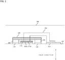
Fig. 1 is a side sectional view of an electronic module that can be used in the first embodiment of the present invention. -
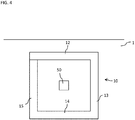
Fig. 2 is a plan view of a detection part that can be used in the first embodiment of the present invention. -
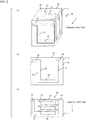
Fig. 3(a) is a perspective plane of an electronic module that can be used in the first embodiment of the present invention,Fig. 3(b) is a vertical sectional view of the electronic module shown inFig. 3(a), and Fig. 3(c) is a plan view of the electronic module shown inFig. 3(a) . InFig. 3(a) , the right part ofFigs. 3(b) and 3(c) is not shown in order to show a vertical cross section different from that ofFig. 3(b) . -
Fig. 4 is a vertical cross-sectional view of yet another detection part that can be used in the first embodiment of the present invention. InFig. 4 , in order to show that the winding return wire part passes through the winding wire part, the second straight part on the front face side of the paper surface, which cannot be seen in the vertical cross section, is also shown. -
Fig. 5 is a diagram showing a relationship between a detection part and an integration circuit that can be used in the first embodiment of the present invention. -
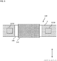
Fig. 6 is an enlarged side sectional view of part of a detection part and a connection body of the electronic module that can be used in the first embodiment of the present invention. -
Fig. 7 is a side sectional view of an electronic module that can be used in the second embodiment of the present invention. -
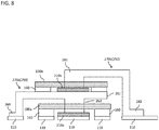
Fig. 8 is a side sectional view of an electronic module that can be used in the third embodiment of the present invention. -
Fig. 9(a) is an enlarged side sectional view of part of a first detection part and a first connection body that can be used in the third embodiment of the present invention,Fig. 9(b) is an enlarged side sectional view of part of a second detection part and a second connection body that can be used in the third embodiment of the present invention. -
Fig. 10 is a side sectional view of an electronic module that can be used in the fourth embodiment of the present invention. -
Fig. 11 is a side sectional view of a detection part that can be used in the fourth embodiment of the present invention. -
Fig. 12 is a side sectional view of an electronic module that can be used in the fourth embodiment of the present invention in an aspect different from that ofFig. 10 . -
Fig. 13 is a plan view of a detection part that can be used in the fifth embodiment of the present invention. -
Fig. 14 is a plan view of a detection part that can be used in the fifth embodiment of the present invention in an aspect different from that ofFig. 13 . -
Fig. 15 is a vertical cross section of a semiconductor device that can be used in the sixth embodiment of the present invention. -
Fig. 16 is a vertical cross section of another semiconductor device that can be used in the sixth embodiment of the present invention in an aspect different from that ofFig. 15 . -
Fig. 17 is a vertical cross section of a semiconductor device that can be used in the sixth embodiment of the present invention in an aspect different from those ofFigs. 15 and16 . -
Fig. 18 is a plan view of a detection part that can be used in the seventh embodiment of the present invention. -
Fig. 19(a) is a vertical cross-sectional view taken along straight line A-A ofFig. 18 , andFig. 19(b ) is a vertical cross-sectional view taken along straight line B-B ofFig. 18 . - In the present embodiment, the "one side" means the upper side of
Fig. 1 , and the "other side" means the lower side ofFig. 1 . In addition, the vertical direction inFig. 1 (the direction from the other side to the one side and the direction from the one side to the other side) is referred to as the "first direction", the in-plane direction including the second direction and the third direction (seeFig. 2 ) orthogonal to the first direction is referred to as the "in-plane direction", and the view from above inFig. 1 is referred to as the "plan view". - The electronic module of the embodiment may have a
conductor layer 110 made of a metal layer such as copper, anelectronic element 210 provided on theconductor layer 110 via a conductive adhesive (not shown) such as solder, aconnection body 250 provided on the front face (upper face ofFig. 1 ) of theelectronic element 210, and adetection part 100 provided so as to surround theconnection body 250. Thedetection part 100 may have a windingwire part 10 provided so as to surround theconnection body 250, and a windingreturn wire part 50 which is connected to the terminal end part of the windingwire part 10 and returns from the terminal end part toward the starting end part. As shown inFig. 6 , thedetection part 100 may have anopening 190 through which theconnection body 250 passes. - The
electronic element 210 may have afirst element electrode 211a on the front face and asecond element electrode 211b on the back face (lower face inFig. 1 ). Thefirst element electrode 211a may be connected to theconnection body 250 via a conductive adhesive, thesecond element electrode 211b may be connected to theconductor layer 110 via a conductive adhesive. Thefirst element electrode 211a is, for example, a source electrode of the MOSFET, and thesecond element electrode 211b is, for example, a drain electrode of the MOSFET. In another example, thefirst element electrode 211a is, for example, a drain electrode of the MOSFET, and thesecond element electrode 211b is, for example, a source electrode of the MOSFET. - As shown in
Fig. 1 , aplacement part 160 on which thedetection part 100 is placed may be provided. Theplacement part 160 may be provided on theconductor layer 110, or theplacement part 160 may be directly placed on asubstrate 105 on which theconductor layer 110 is provided. The electronic module may have a sealingpart 140 made of a sealing resin that seals thedetection part 100, theconnection body 250, and the like. - As shown in
FIG. 3 , thedetection part 100 of the present embodiment may have asemiconductor layer 1, and the windingwire part 10 and the windingreturn wire part 50 may be formed in thesemiconductor layer 1. As a material of the semiconductor, a material such as silicon, silicon carbide, gallium nitride or the like can be used. - The winding
wire part 10 and the windingreturn wire part 50 may be formed of a semiconductor material such as polysilicon, but not limited thereto. They may be formed of a metal material such as copper and aluminum, and the metal film may be the windingwire part 10 and the windingreturn wire part 50. - The winding
return wire part 50 may not pass through the windingwire part 10. In the present embodiment, as shown inFig. 2 , the windingreturn wire part 50 is provided so as to surround the outer periphery of the windingwire part 10. The inside of the windingwire part 10 may be filled with an insulating material such as an oxide film. In an aspect shown inFig. 3 , a first insulatingfilm 91 provided on part of the outer periphery and the bottom face of the windingwire part 10, a second insulatingfilm 92 provided on the first insulatingfilm 91, and a third insulatingfilm 93 that fills the inside of the windingwire part 10 are provided. - In
Fig. 1 , although the description is made using an aspect in which the windingreturn wire part 50 does not pass through the windingwire part 10, the present invention is not limited to this. As shown inFig. 4 , an aspect in which the windingreturn wire part 50 passes through the windingwire part 10 may be used. In the present embodiment, an aspect shown inFig. 3 is referred to as a "pseudo Rogowski coil", and an aspect shown inFig. 4 is referred to as a "Rogowski coil". The references numerals "10, 50" are used inFig. 6 , which means that the pseudo Rogowski coil may be used for these, or the Rogowski coil may be used. In the embodiment, although the description will be made mainly by using an aspect in which the Rogowski coil or the pseudo Rogowski coil is formed of a semiconductor material, the present invention is not limited to this. An aspect in which the Rogowski coil or the pseudo Rogowski coil is formed in a flexible substrate may be used, or the previously known Rogowski coil may be used. A change in current can be detected by using the Rogowski coil or the pseudo Rogowski coil as thedetection part 100, but the detection is not limited to be performed by the change in the current. A change in another event (change in an electric signal) such as a change in the magnetic field may be detected. In this case, the change in the magnetic field due to the change in the current may be detected, or the change in the magnetic field may be detected regardless of the change in the current. - As shown in
Fig 3 , the windingwire part 10 may have: a firststraight part 11 along a winding direction; a secondstraight part 12 extending toward the peripherally inward (to the right inFig 3 ) from the end of the firststraight part 11 and extending in a plane direction (direction including the second direction and the third direction) along the winding direction; a thirdstraight part 13 extending from one side toward the other side from the end of the secondstraight part 12; a fourthstraight part 14 extending toward the peripherally outward (to the left side inFig 3 ) from the end of the thirdstraight part 13 and extending in the plane direction along the direction perpendicular to the winding direction; and a fifthstraight part 15 extending from the other side toward one side from the end of the fourth straight part 14 (first aspect). Further, a sixthstraight part 16 extending toward the peripherally outward from the end of the fifthstraight part 15 in the plane direction may be provided at the terminal end part of the windingwire part 10, and the end of the sixthstraight part 16 and the starting end part of the windingreturn wire part 50 may be connected to each other. The windingreturn wire part 50 may extend in the plane direction. - In an aspect shown in
Fig. 3 , when viewed in the vertical section, an aspect is used in which a rectangular shape is formed by a secondstraight part 12, a thirdstraight part 13, a fourthstraight part 14, and a fifthstraight part 15, but the present invention is not limited to such an aspect. The shape may be triangular when viewed in vertical section, or it may be a polygon with more corners (pentagon or more). - As shown in
Fig. 5 , the windingreturn wire part 50 and the windingwire part 10 of thesemiconductor layer 1 of the present embodiment are connected to aresistor part 125, acapacitor 120 and anoperational amplifier 130 which are provided outside, so that an integration circuit may be formed. Not limited to such an aspect, theresistor part 125 or thecapacitor 120, or theresistor part 125 and thecapacitor 120 of the integration circuit may be formed on thesemiconductor layer 1. As an example, inFig. 5 , a windingwire electrode pad 19 connected to the starting end part of the windingwire part 10 is connected to theresistor part 125, and theresistor part 125 is connected to thecapacitor 120 and the inverting input terminal of theoperational amplifier 130, and a winding returnwire electrode pad 59 connected to the terminal end part of the windingreturn wire part 50 is connected to the noninverting input terminal of theoperational amplifier 130. - As shown in
Fig. 2 , the windingwire part 10 may have an A-direction windingwire part 31 extending in the second direction, a B-direction windingwire part 32 connected to the end of the A-direction windingwire part 31 and extending in the third direction, a C-direction windingwire part 33 connected to the end of the B-direction windingwire part 32 and extending in the second direction, and a D-direction windingwire part 34 connected to the end of the C-direction windingwire part 33 and extending in the third direction. When the aspect described above is employed, each of the direction windingwire parts 31 to 34 can be linearly formed, which is advantageous in that they can be manufactured relatively easily. The present embodiment describes the aspect using four direction windingwire parts 31 to 34. However, the present invention is not limited thereto, and three direction windingwire parts 10 may be used to form a triangular shape in the plane direction, or five or more direction windingwire parts 10 may be used to form a polygonal shape in the plane direction. - The A-direction winding
wire part 31, the B-direction windingwire part 32, the C-direction windingwire part 33, and the D-direction windingwire part 34 may correspond to each other in length. The state where they correspond to each other in length indicates that the length of the A-direction windingwire part 31, the length of the B-direction windingwire part 32, the length of the C-direction windingwire part 33, and the length of the D-direction windingwire part 34 are respectively within the range of ±5% of the average value of the A-direction windingwire part 31, the B-direction windingwire part 32, the C-direction windingwire part 33, and the D-direction windingwire part 34. The numbers of turns included in the A-direction windingwire part 31, the B-direction windingwire part 32, the C-direction windingwire part 33, and the D-direction windingwire part 34 may be the same. Since the A-direction windingwire part 31 is connected to the winding-wire electrode pad 19, the number of turns of the A-direction windingwire part 31 may be less than the numbers of turns of the B-direction windingwire part 32, the C-direction windingwire part 33, and the D-direction windingwire part 34 by, for example, one, two, or more. - Subsequently, an example of the effect according to the present embodiment configured as described above will be described. All the aspects to be described in "effect" can be employed in the above configuration.
- In the embodiment as shown in
Fig. 1 , when an aspect in which thedetection part 100 having the windingwire part 10 and the windingreturn wire part 50 is provided so as to surround theconnection body 250 which is electrically connected to theelectronic element 210 is used, the change in the current flowing through theelectronic element 210 can be detected accurately without the size too large. - Specifically, when an aspect in which the winding
wire part 10 is provided on thesemiconductor layer 1 is used, the configuration of the windingwire part 10 can be miniaturized by using the manufacturing technology of semiconductor devices, so that the number of turns can be increased per unit length. Therefore, the change in current can be detected with high accuracy. Further, since the miniaturization is possible in this way, even when the windingwire part 10 and the windingreturn wire part 50 are provided on thesemiconductor layer 1, it is possible to prevent the size from becoming large. - As shown in
Fig. 6 , when an aspect in which anopening 190 through which theconnection body 250 passes is provided in thedetection part 100, and thedetection part 100 is provided so as to surround theconnection body 250 is used, thedetection part 250 can detect a change in the current flowing in theconnection body 250 whose position in the in-plane direction is fixed to some extent, so that highly accurate detection can be realized. - As shown in
Fig. 2 , when an aspect in which the windingreturn wire part 50 does not pass through the windingwire part 10 is used, the configuration is very advantageous in that the manufacturing process can be facilitated. In other words, as shown inFig. 4 , when an aspect in which the windingreturn wire part 50 passes through the windingwire part 10 is used, the process of forming the windingreturn wire part 50 in the windingwire part 10 is complicated, so that the manufacturing cost goes up. On the other hand, when the windingreturn wire part 50 is not formed in the windingwire part 10, the manufacturing process can be performed much easier, so that the configuration is advantageous in that the manufacturing cost can be reduced. - When the
electronic element 210 is a switching element such as a MOSFET, the current changes when switching between ON and OFF, so that it is advantageous to employ the quasi Rogowski coil and the Rogowski coil in the present embodiment. - When as shown in
Figs. 3(a) and 3(b) , an aspect is employed in which the height positions of the firststraight part 11, the secondstraight part 12, and the sixthstraight part 16 of the windingwire part 10, and the height position of the windingreturn wire part 50 are the same, this is advantageous in that the same steps can be used for these. That is, this is advantageous in that a forming process can be performed by stacking the conductive material on the upper face of the first insulatingfilm 91 and etching the conductive material. - In this embodiment, when an aspect is employed in which the winding
return wire part 50 can be positioned outward of the periphery of the windingwire part 10, this is advantageous in that the windingwire part 10 can be disposed as close as possible to the current flowing between thefirst element electrode 61 and thesecond element electrode 62. - Next, a second embodiment of the present invention will be described.
- In the embodiment, as shown in
Fig. 7 , aconnection body 260 has ahead part 261 and apillar part 262 extending from thehead part 261 in the thickness direction of thehead part 261. The windingwire part 10 and the windingreturn wire part 50 of thedetection part 100 are provided so as to surround thepillar part 262 passing through theopening 190. Theelectronic element 210 may have a firstelectronic element 210a and a secondelectronic element 210b provided in the front face side of the firstelectronic element 210a. Thepillar part 262 may be provided on the firstelectronic element 210a, and the secondelectronic element 210b may be provided on thehead part 261. Any configuration used in the first embodiment can also be used in the second embodiment. The members described in the first embodiment will be described with the same reference numerals. - According to the embodiment, the first
electronic element 210a and the secondelectronic element 210b can be laminated and disposed, and thedetection part 100 can detect a change in the current flowing between the firstelectronic element 210a and the secondelectronic element 210b. The secondelectronic element 210b can be disposed in a stable state by providing thehead part 261 as in the present embodiment, and the size of theopening 190 is not increased by providing thepillar part 262. As a result, the windingwire part 10 and the windingreturn wire part 50 can be provided in a compact state in the in-plane direction. - Each of the first
electronic element 210a and the secondelectronic element 210b may be a switching element such as a MOSFET. In this case, for example, the source electrode provided on the front face of the firstelectronic element 210a and the drain electrode provided on the back face of the secondelectronic element 210b may be connected through theconnection body 260. As another example, the drain electrode provided on the front face of the firstelectronic element 210a and the source electrode provided on the back face of the secondelectronic element 210b may be connected through theconnection body 260. - Next, a third embodiment of the present invention will be described.
- In each of the above embodiments, as shown in
Fig. 8 , theconnection body 250 has afirst connection body 270a provided on the front face of the firstelectronic element 210a, and asecond connection body 270b provided on the front face of the secondelectronic element 210b. As shown inFig. 9 , thedetection part 100 has afirst detection part 100a having a first windingwire part 10a and a first windingreturn wire part 50a surrounding thefirst connection body 270a, and asecond detection part 100b having a second windingwire part 10b and a second windingreturn wire part 50b surrounding thesecond connection body 270b. As an example, thesecond connection body 270b is a connector connected to the front face of the secondelectronic element 210b. Thesecond connection body 270b has a second connectiondistal end part 281 passing through theopening 190 of thesecond detection part 100b, and a second connectionproximal end part 282 provided on theconductor layer 110 via a conductive adhesive. Thefirst connection body 270a has thehead part 261, thepillar part 262 extending from thehead part 261 in the thickness direction of thehead part 261, and a first connectionproximal end part 269 provided on theconductor layer 110 via a conductive adhesive. Thepillar part 262 is provided on the front face of the firstelectronic element 210a, and the secondelectronic element 210b is provided on thehead part 261. - According to the embodiment, the first
electronic element 210a and the secondelectronic element 210b can be laminated and disposed, and thefirst detection part 100a can detect a change in the current flowing between the firstelectronic element 210a and the secondelectronic element 210b. Further, thesecond detection part 100b can detect the change in the current flowing through the secondelectronic element 210b. Therefore, according to this aspect, it is possible to more reliably detect the change in current with respect to each of the firstelectronic element 210a and the secondelectronic element 210b laminated. - The size of the second connection
distal end part 282 of thesecond connection body 270b and the size of thepillar part 262 of thefirst connection body 270a may be substantially the same. When such an aspect is used, the configuration is advantageous in that a change in the current flowing through the second connectiondistal end part 282 and a change in the current flowing through thepillar part 262 of thefirst connection body 270a can be detected with the same degree of accuracy. Specifically, when thefirst detection part 100a and thesecond detection part 100b are made of the same member, the configuration is advantageous in that it is possible to detect a change in the current flowing through the second connectiondistal end part 282 and a change in the current flowing through thepillar part 262 with substantially the same accuracy by making the sizes of the second connectiondistal end part 282 and thepillar part 262 substantially the same in this way. Note that the fact that the "sizes" are "almost the same" means that the difference between the two "sizes" is within 5% of the larger "size". The fact that the size W1 and the size W2 (W1 ≥ W2) are substantially the same means that W1 × 0.95 ≤ W2 ≤ W1. - Next, a fourth embodiment of the present invention will be described.
- In the embodiment, as shown in
Fig. 10 , theelectronic element 210 having thesecond element electrode 211b provided on the back face side, and thedetection part 100 on which thesecond element electrode 211b of theelectronic element 210 is placed may be provided. As shown inFig. 11 , thedetection part 100 of the present embodiment has afirst detection electrode 61 on which thesecond element electrode 211b of theelectronic element 210 is placed, aconductor part 63 through which the current flowing into theelectronic element 210 passes, the windingwire part 10 provided so as to surround theconductor part 63, and the windingreturn wire part 50 which is connected at the terminal end part of the windingwire part 10 and returns from the terminal end part toward the starting end part. Any configuration used in each of the above embodiments can also be used in the embodiment. The members described in each of the above embodiments will be described with the same reference numerals. - The
detection part 100 may have asecond detection electrode 63 on the back face side. Thesecond detection electrode 63 may be placed on theconductor layer 110 via a conductive adhesive. Theconductor part 63 may be made of a metal material or a semiconductor material. When theconductor part 63 is made of a semiconductor material, an aspect may be used in which the impurity concentration of theconductor part 63 is higher than that of thesemiconductor layer 1 in the peripheral region surrounding theconductor part 63. - As shown in
Fig. 12 , aconnector 290 connected to the windingwire electrode pad 19 and/or theconnector 290 connected to the winding returnwire electrode pad 59 may be provided. In this case, theresistor part 125, thecapacitor 120, and theoperational amplifier 130 may be connected to the windingwire part 10 and the windingreturn wire part 50 through theconnector 290 and theconductor layer 110. - Next, a fifth embodiment of the present invention will be described.
- In the first embodiment, as an example, the
detection part 100 is configured as shown inFig. 2 . As shown inFig. 13 , an aspect in which the windingreturn wire part 50 is provided inside the peripheral edge of the windingwire part 10 may be used. Further, as shown inFig. 14 , each of the windingwire part 10 and the windingreturn wire part 50 may have a circular shape in a plan view (a plane including the second direction and the third direction). Further, each of the windingwire part 10 and the windingreturn wire part 50 may have a triangular shape in a plan view. Any configuration used in each of the above embodiments can also be used in the embodiment. - Next, a sixth embodiment of the present invention will be described.
- In the above respective embodiments, one quasi Rogowski coil or Rogowski coil is provided. In contrast, in the sixth embodiment, a plurality of quasi Rogowski coils or Rogowski coils are provided. Any configurations adopted in the above respective embodiments can also be adopted in the present embodiment. The members described in each of the above respective embodiments will be described with the same reference numerals.
- As shown in
Fig. 15 , quasi Rogowski coils or Rogowski coils may be aligned in the first direction. More specifically, the windingwire part 10 and the windingreturn wire part 50 which does not pass through the winding wire part 10 (a quasi Rogowski coil), or the windingwire part 10 and the windingreturn wire part 50 passing through the winding wire part 10 (Rogowski coil) may be aligned in the first direction. When this aspect is adopted, a change in current can be detected at two or more locations in the first direction, which is advantageous in that a change in current can be detected more accurately. However, in this aspect, it should be noted that, since the windingwire part 10 and the windingreturn wire part 50 need to be arranged so as to be stacked in the first direction, the manufacturing process becomes complicated as compared with the first embodiment. - As shown in
Fig. 16 , another quasi Rogowski coil or Rogowski coil may be disposed on the outer peripheral side of the quasi Rogowski coil or Rogowski coil. More specifically, the windingwire part 10 and the windingreturn wire part 50 which does not pass through the winding wire part 10 (quasi Rogowski coil), or the windingwire part 10 and the windingreturn wire part 50 passing through the winding wire part 10 (Rogowski coil) may be aligned in the second direction or the third direction. When this aspect is adopted, a change in current can also be detected more accurately, which is advantageous. In addition, this aspect is also advantageous in that the similar manufacturing process as that of the first embodiment can be employed. - These aspects may be combined, and as shown in
Fig. 17 , the quasi Rogowski coils or Rogowski coils may be stacked in the first direction, and other quasi Rogowski coils or Rogowski coils may be provided on the outer peripheral side of the quasi Rogowski coils or Rogowski coils. More specifically, the windingwire parts 10 and the windingreturn wire parts 50 which do not pass through the winding wire parts 10 (quasi Rogowski coils), or the windingwire parts 10 and the windingreturn wire parts 50 passing through the winding wire parts 10 (Rogowski coils) may be aligned in the second direction or the third direction, and also aligned in the first direction. In addition, inFigs. 15 and16 , an aspect in which theopening 190 is provided, and theconnection body 250 passes through theopening 190 is described, and inFig. 17 , an aspect in which afirst element electrode 61, asecond element electrode 62, and theconductor part 63 are provided is described. - Next, the seventh embodiment of the present invention will be described.
- In the present embodiment, as shown in
Figs. 18 and19 , the windingreturn wire part 50 is positioned on the one side of the windingwire part 10. Any configuration used in each of the above embodiments can also be used in the embodiment. The members described in each of the above embodiments will be described with the same reference numerals. As a modification of the present embodiment, the windingreturn wire part 50 may be positioned on the other side of the windingwire part 10. - As shown in
Fig. 19 , the terminal end part of the windingwire part 10 and the starting end part of the windingreturn wire part 50 may be connected by a connectingbody 18 extending in the first direction. The conductive material used to form the connectingbody 18 may be the same material as the conductive material used when forming the windingwire part 10, or may be a different material. - The foregoing descriptions of the embodiments and the disclosure of the drawings are merely one example for describing the present invention recited in the claims. The present invention recited in the claims shall not be limited by the foregoing descriptions of the embodiments and the disclosure of the drawings. Further, the recitations of the claims at the time of the filing of the present application are merely an example, and the recitations of the claims can be changed as appropriate based on the description of the specification, the drawings, and the like.
-
- 1
- semiconductor layer
- 10
- winding wire part
- 10a
- first winding wire part
- 10b
- second winding wire part
- 50
- winding return wire part
- 50a
- first winding return wire part
- 50b
- second winding return wire part
- 61
- first detection electrode
- 62
- second detection electrode
- 63
- conductor part
- 100
- detection part
- 100a
- first detection part
- 100b
- second detection part
- 210
- electronic element
- 210a
- first electronic element
- 210b
- second electronic element
- 211b
- second element electrode
- 250, 260
- connection body
- 261
- head part
- 262
- pillar part
- 270a
- first connection body
- 270b
- second connection body
Claims (8)
- An electronic module comprising:an electronic element;a connection body provided on a front face of the electronic element; anda detection part having a winding wire part provided so as to surround the connection body, and a winding return wire part connected to a terminal end part of the winding wire part and returns from the terminal end part toward a starting end part.
- The electronic module according to claim 1, wherein
the connection body has a head part and a pillar part extending from the head part in a thickness direction of the head part, and
the winding wire part and the winding return wire part are provided so as to surround the pillar part. - The electronic module according to claim 2, wherein
the electronic element has a first electronic element on which the pillar part is provided, and a second electronic element which is provided on the head part. - The electronic module according to claim 1, wherein
the electronic element has a first electronic element and a second electronic element provided in a front face side of the first electronic element,
the connection body has a first connection body provided on a front face of the first electronic element, and a second connection body provided on a front face of the second electronic element, and
the detection part has a first detection part having a first winding wire part and a first winding return wire part surrounding the first connection body, and a second detection part having a second winding wire part and a second winding return wire part surrounding the second connection body. - The electronic module according to claim 4, wherein
the second connection body is a connector connected to a front face of the second electronic element. - The electronic module according to claim 4, wherein
the first connection body has a head part and a pillar part extending from the head part in a thickness direction of the head part,
the pillar part is provided on a front surface of the first electronic element, and
the second electronic element is provided on the head part. - The electronic module according to claim 1, wherein
the winding return wire part does not pass through the winding wire part in the detection part. - An electronic module comprising:an electronic element having a second element electrode provided on a back face side; anda detection part having a first detection electrode on which the second element electrode of the electronic element is placed, a conductor part through which current flowing into the electronic element passes, a winding wire part provided so as to surround the conductor part, and a winding return wire part which is connected at a terminal end part of the winding wire part and returns from the terminal end part toward a starting end part.
Applications Claiming Priority (1)
| Application Number | Priority Date | Filing Date | Title |
|---|---|---|---|
| PCT/JP2018/025306 WO2020008544A1 (en) | 2018-07-04 | 2018-07-04 | Electronic module |
Publications (2)
| Publication Number | Publication Date |
|---|---|
| EP3819651A1 true EP3819651A1 (en) | 2021-05-12 |
| EP3819651A4 EP3819651A4 (en) | 2022-03-16 |
Family
ID=69060826
Family Applications (1)
| Application Number | Title | Priority Date | Filing Date |
|---|---|---|---|
| EP18925535.9A Withdrawn EP3819651A4 (en) | 2018-07-04 | 2018-07-04 | Electronic module |
Country Status (5)
| Country | Link |
|---|---|
| US (1) | US11486904B2 (en) |
| EP (1) | EP3819651A4 (en) |
| JP (1) | JP7572240B2 (en) |
| CN (1) | CN112352163B (en) |
| WO (1) | WO2020008544A1 (en) |
Families Citing this family (1)
| Publication number | Priority date | Publication date | Assignee | Title |
|---|---|---|---|---|
| WO2022186082A1 (en) * | 2021-03-05 | 2022-09-09 | 富士電機機器制御株式会社 | Current sensor and manufacturing method of current sensor |
Family Cites Families (17)
| Publication number | Priority date | Publication date | Assignee | Title |
|---|---|---|---|---|
| JP3193217B2 (en) * | 1993-12-16 | 2001-07-30 | 三菱電機株式会社 | Current detector |
| JP2001343401A (en) * | 2000-05-31 | 2001-12-14 | Mitsubishi Electric Corp | Current detector |
| JP2002082134A (en) * | 2000-09-08 | 2002-03-22 | Mitsubishi Heavy Ind Ltd | Current sensor, current-measuring method and switch circuit |
| JP2004119926A (en) | 2002-09-30 | 2004-04-15 | Toshiba Corp | Current transformer and current transformer system |
| WO2005103737A1 (en) * | 2004-04-24 | 2005-11-03 | Werner Zumbrunn | Sensor for alternating currents |
| JP4622839B2 (en) | 2005-12-12 | 2011-02-02 | 日新電機株式会社 | Rogowski coil, Rogowski coil production method, and current measuring device |
| JP4710996B2 (en) * | 2009-03-09 | 2011-06-29 | パナソニック電工株式会社 | Current sensor |
| JP5547031B2 (en) | 2010-10-21 | 2014-07-09 | 日置電機株式会社 | Rogowski coil and current detector |
| JP5817363B2 (en) * | 2011-02-25 | 2015-11-18 | 株式会社豊田中央研究所 | Current measurement probe |
| CN103827990A (en) * | 2011-07-16 | 2014-05-28 | Abb技术股份公司 | Electrical device |
| JP2013130571A (en) * | 2011-11-23 | 2013-07-04 | Nippon Soken Inc | Current sensor |
| CN103630723A (en) * | 2013-11-25 | 2014-03-12 | 北京航空航天大学 | Rogowski coil sensing head suitable for Rogowski coil current sensor |
| JP6361825B2 (en) | 2015-05-28 | 2018-07-25 | 株式会社村田製作所 | Current detection element, power transmission device and power transmission system |
| JP6415467B2 (en) * | 2016-02-24 | 2018-10-31 | 日本特殊陶業株式会社 | Wiring board and semiconductor module |
| JP6777525B2 (en) * | 2016-12-21 | 2020-10-28 | 日本碍子株式会社 | Heat resistant element for current detection |
| JP6732104B2 (en) * | 2017-11-24 | 2020-07-29 | 新電元工業株式会社 | Semiconductor device and semiconductor component |
| FR3075387B1 (en) * | 2017-12-14 | 2019-11-08 | Schneider Electric Industries Sas | ELECTRIC CURRENT MEASURING DEVICE, CURRENT MEASURING APPARATUS, AND METHOD FOR MANUFACTURING CURRENT MEASURING DEVICE |
-
2018
- 2018-07-04 JP JP2020528585A patent/JP7572240B2/en active Active
- 2018-07-04 US US17/257,177 patent/US11486904B2/en active Active
- 2018-07-04 WO PCT/JP2018/025306 patent/WO2020008544A1/en not_active Ceased
- 2018-07-04 EP EP18925535.9A patent/EP3819651A4/en not_active Withdrawn
- 2018-07-04 CN CN201880095014.2A patent/CN112352163B/en active Active
Also Published As
| Publication number | Publication date |
|---|---|
| US11486904B2 (en) | 2022-11-01 |
| WO2020008544A1 (en) | 2020-01-09 |
| JPWO2020008544A1 (en) | 2021-11-04 |
| EP3819651A4 (en) | 2022-03-16 |
| CN112352163B (en) | 2024-05-28 |
| JP7572240B2 (en) | 2024-10-23 |
| US20210123954A1 (en) | 2021-04-29 |
| CN112352163A (en) | 2021-02-09 |
Similar Documents
| Publication | Publication Date | Title |
|---|---|---|
| US10753963B2 (en) | Current sensor isolation | |
| US9476915B2 (en) | Magnetic field current sensors | |
| US11094447B2 (en) | Chip inductor and method for manufacturing the same | |
| EP2402778A1 (en) | Magnetoimpedance sensor element and method for manufacturing the same | |
| KR20180064297A (en) | Integrated circuit package comprising lead frame | |
| JP7385368B2 (en) | Current detector and power module | |
| US11360122B2 (en) | Current sensor and method for manufacturing current sensor | |
| US11300593B2 (en) | Semiconductor component, assembly and method for manufacturing semiconductor component | |
| US11486904B2 (en) | Electronic module | |
| CN114502909B (en) | Displacement sensor and displacement sensor system | |
| US11268988B2 (en) | Detection substrate, assembly, and method for manufacturing detection substrate | |
| US9417296B2 (en) | Magnetic sensor and manufacturing method thereof | |
| US11280812B2 (en) | Semiconductor device and semiconductor component | |
| CN117222897B (en) | Rogowski type current sensor, inverter and method for installing Rogowski type current sensor | |
| JP7319771B2 (en) | Current detector and power module | |
| JP7560340B2 (en) | Current detector and power module | |
| CN117214500A (en) | Current detector and power module | |
| TW202349009A (en) | Current detector and power module that achieve high-precision current detection and allow easy installation even in a ring-shaped state after resin sealing |
Legal Events
| Date | Code | Title | Description |
|---|---|---|---|
| STAA | Information on the status of an ep patent application or granted ep patent |
Free format text: STATUS: THE INTERNATIONAL PUBLICATION HAS BEEN MADE |
|
| PUAI | Public reference made under article 153(3) epc to a published international application that has entered the european phase |
Free format text: ORIGINAL CODE: 0009012 |
|
| STAA | Information on the status of an ep patent application or granted ep patent |
Free format text: STATUS: REQUEST FOR EXAMINATION WAS MADE |
|
| 17P | Request for examination filed |
Effective date: 20210203 |
|
| AK | Designated contracting states |
Kind code of ref document: A1 Designated state(s): AL AT BE BG CH CY CZ DE DK EE ES FI FR GB GR HR HU IE IS IT LI LT LU LV MC MK MT NL NO PL PT RO RS SE SI SK SM TR |
|
| DAV | Request for validation of the european patent (deleted) | ||
| DAX | Request for extension of the european patent (deleted) | ||
| A4 | Supplementary search report drawn up and despatched |
Effective date: 20220210 |
|
| RIC1 | Information provided on ipc code assigned before grant |
Ipc: G01R 15/18 20060101AFI20220204BHEP |
|
| GRAP | Despatch of communication of intention to grant a patent |
Free format text: ORIGINAL CODE: EPIDOSNIGR1 |
|
| STAA | Information on the status of an ep patent application or granted ep patent |
Free format text: STATUS: GRANT OF PATENT IS INTENDED |
|
| INTG | Intention to grant announced |
Effective date: 20240112 |
|
| STAA | Information on the status of an ep patent application or granted ep patent |
Free format text: STATUS: THE APPLICATION IS DEEMED TO BE WITHDRAWN |
|
| 18D | Application deemed to be withdrawn |
Effective date: 20240514 |