EP3817343A1 - Mobile terminal - Google Patents
Mobile terminal Download PDFInfo
- Publication number
- EP3817343A1 EP3817343A1 EP19800361.8A EP19800361A EP3817343A1 EP 3817343 A1 EP3817343 A1 EP 3817343A1 EP 19800361 A EP19800361 A EP 19800361A EP 3817343 A1 EP3817343 A1 EP 3817343A1
- Authority
- EP
- European Patent Office
- Prior art keywords
- mobile terminal
- circuit board
- gap
- infrared sensor
- terminal according
- Prior art date
- Legal status (The legal status is an assumption and is not a legal conclusion. Google has not performed a legal analysis and makes no representation as to the accuracy of the status listed.)
- Granted
Links
Images

Classifications
-
- H—ELECTRICITY
- H04—ELECTRIC COMMUNICATION TECHNIQUE
- H04M—TELEPHONIC COMMUNICATION
- H04M1/00—Substation equipment, e.g. for use by subscribers
- H04M1/02—Constructional features of telephone sets
- H04M1/0202—Portable telephone sets, e.g. cordless phones, mobile phones or bar type handsets
- H04M1/026—Details of the structure or mounting of specific components
- H04M1/0266—Details of the structure or mounting of specific components for a display module assembly
-
- H—ELECTRICITY
- H04—ELECTRIC COMMUNICATION TECHNIQUE
- H04M—TELEPHONIC COMMUNICATION
- H04M1/00—Substation equipment, e.g. for use by subscribers
- H04M1/02—Constructional features of telephone sets
- H04M1/0202—Portable telephone sets, e.g. cordless phones, mobile phones or bar type handsets
- H04M1/026—Details of the structure or mounting of specific components
-
- H—ELECTRICITY
- H04—ELECTRIC COMMUNICATION TECHNIQUE
- H04M—TELEPHONIC COMMUNICATION
- H04M1/00—Substation equipment, e.g. for use by subscribers
- H04M1/02—Constructional features of telephone sets
- H04M1/0202—Portable telephone sets, e.g. cordless phones, mobile phones or bar type handsets
- H04M1/026—Details of the structure or mounting of specific components
- H04M1/0264—Details of the structure or mounting of specific components for a camera module assembly
-
- H—ELECTRICITY
- H04—ELECTRIC COMMUNICATION TECHNIQUE
- H04M—TELEPHONIC COMMUNICATION
- H04M1/00—Substation equipment, e.g. for use by subscribers
- H04M1/02—Constructional features of telephone sets
- H04M1/0202—Portable telephone sets, e.g. cordless phones, mobile phones or bar type handsets
- H04M1/026—Details of the structure or mounting of specific components
- H04M1/0277—Details of the structure or mounting of specific components for a printed circuit board assembly
-
- H—ELECTRICITY
- H04—ELECTRIC COMMUNICATION TECHNIQUE
- H04M—TELEPHONIC COMMUNICATION
- H04M2250/00—Details of telephonic subscriber devices
- H04M2250/12—Details of telephonic subscriber devices including a sensor for measuring a physical value, e.g. temperature or motion
Definitions
- This disclosure relates to the field of communications technologies, and in particular, to a mobile terminal.
- photosensitive devices such as an infrared sensor or a photosensitive sensor
- different photosensitive devices can implement different functions.
- a photosensitive device of the mobile terminal in the related art is generally arranged on the front side of the mobile terminal, which limits a screen-to-body ratio of the whole terminal, resulting in a relatively low screen-to-body ratio of the mobile terminal.
- Embodiments of this disclosure provide a mobile terminal, to resolve a problem of a relatively low screen-to-body ratio of the mobile terminal because a photosensitive device of the mobile terminal is generally arranged on the front side of the mobile terminal.
- a mobile terminal includes a cover plate, a display screen, a middle frame, an edge frame, and a photosensitive device, where the cover plate is fixedly connected to the edge frame, the display screen is located between the cover plate and the middle frame, a first gap is provided between the display screen and the edge frame, a second gap is provided between the middle frame and the edge frame, and the first gap and the second gap are connected to form an optical channel for the photosensitive device.
- the photosensitive device does not need to be arranged on the front side of the mobile terminal, so that the screen-to-body ratio of the mobile terminal can be increased.
- FIG. 1 is a schematic structural diagram of a mobile terminal according to an embodiment of this disclosure.
- the mobile terminal includes a cover plate 1, a display screen 2, a middle frame 3, an edge frame 4, and a photosensitive device 5.
- the cover plate 1 is fixedly connected to the edge frame 4
- the display screen 2 is located between the cover plate 1 and the middle frame 3
- a first gap is provided between the display screen 2 and the edge frame 4
- a second gap is provided between the middle frame 3 and the edge frame 4
- the first gap and the second gap are connected to form an optical channel for the photosensitive device 5.
- the mobile terminal may further include a circuit board 6 connected to the photosensitive device and a battery cover 7 connected to the edge frame.
- the mobile terminal may use the circuit board 6 to control some internal components of the mobile terminal, and use the battery cover 7 to enclose the internal components.
- the cover plate 1 may be a glass cover plate, or may be a cover plate made of another synthetic material, or the like.
- the display screen 2 may be a liquid crystal display screen, or may be a display screen made of a crystal diode. Materials of the middle frame 3 and the edge frame 4 may be metal, or may be some other synthetic materials, or the like.
- the photosensitive device 5 may be an infrared sensor, or may be a photosensitive sensor, or the like. Certainly, the photosensitive device 5 may alternatively be another photosensitive device. This is not limited in this embodiment of this disclosure.
- the first gap is provided between the display screen 2 and the edge frame 4
- the second gap is provided between the middle frame 3 and the edge frame 4
- the first gap and the second gap are connected to form an optical channel for the photosensitive device 5.
- the first gap and the second gap are both assembly gaps, that is, structural gaps between the display screen, the middle frame, and the edge frame. In this way, light can reach the photosensitive device 5 through the optical channel, so that the photosensitive device 5 can receive the light, and the photosensitive device 5 can also send a signal outward through the optical channel.
- a structural assembly gap (including the first gap and the second gap) is used as the optical channel of the photosensitive device 5, avoiding occupying visual space that is occupied in a longitudinal direction of the mobile terminal in the related art, so that the mobile terminal can have a relatively high screen-to-body ratio.
- the foregoing mobile terminal may be a mobile phone, a tablet computer (Tablet Personal Computer), a laptop computer (Laptop Computer), a personal digital assistant (personal digital assistant, PDA), a mobile internet device (Mobile Internet Device, MID), a wearable device (Wearable Device), or the like.
- the photosensitive device 5 is arranged in the second gap.
- the photosensitive device 5 is arranged in the second gap, so that there is no need to set up independent assembly space for the photosensitive device 5 on a black border of the mobile terminal, and only a structural assembly gap is required to achieve a relatively high screen-to-body ratio for the mobile terminal.
- the photosensitive device 5 is an infrared sensor, a transmit end 51 and a receive end 52 of the infrared sensor face the cover plate 1, and an infrared ray emitted by the infrared sensor may be emitted out of the cover plate 1 through the optical channel.
- the photosensitive device 5 is the infrared sensor, so that the infrared sensor can also be designed to detect a distance when the mobile terminal has a high screen-to-body ratio.
- the transmit end 51 and the receive end 52 of the infrared sensor face the cover plate 1, and the emitted infrared ray may be emitted out of the cover plate 1 through the optical channel.
- the infrared ray emitted by the transmit end 51 encounters an obstacle, the infrared ray can be reflected back and be received by the receive end 52. In this way, the distance is detected.
- the edge frame 4 is provided with a first step structure
- the cover plate 1 is bonded to the first step structure through an adhesive layer 8
- the adhesive layer 8 includes a first side and a second side that are arranged oppositely, where the second side is a side close to the display screen 2, and the first gap is located between the second side and the display screen 2.
- the edge frame 4 is provided with the first step structure, so that the cover plate 1 can be arranged on the first step structure, and the cover plate 1 can be well accommodated.
- the cover plate 1 is bonded to the first step structure through the adhesive layer 8, and the cover plate 1 can be well fixed on the first step structure. When being damaged, the cover plate 1 can be replaced easily.
- the mobile terminal further includes the circuit board 6, the infrared sensor is electrically connected to the circuit board 6, and the circuit board 6 is fixedly connected to the middle frame 3 and the edge frame 4.
- the circuit board 6 may be a common circuit board, may be a flexible circuit board, or may be a reinforcing board of a flexible circuit board, or the like.
- the infrared sensor is electrically connected to the circuit board 6 to ensure that the infrared sensor can work well.
- the circuit board 6 may be fixedly connected, bonded, or connected by small screws, to the middle frame 3 and the edge frame 4.
- the edge frame 4 is provided with a second step structure, the circuit board 6 is fixedly connected to the second step structure, and the circuit board 6 is fixedly connected to a side, facing away from the display screen 2, of the middle frame 3.
- the edge frame 4 is provided with the second step structure, the circuit board 6 is fixedly connected to the second step structure, and the circuit board 6 is fixedly connected to the side, facing away from the display screen 2, of the middle frame 3, so that the circuit board 6 can be well fixed to the middle frame 3 and the edge frame 4.
- a side of the middle frame 3 that is fixedly connected to the circuit board 6 and a side of the edge frame 4 that is fixedly connected to the circuit board may be on one plane, so that the circuit board 6 can be fastened more firmly.
- the infrared sensor is welded to the circuit board 6, and the circuit board 6 is electrically connected to a main board 9.
- the infrared sensor is welded to the circuit board 6, so that the infrared sensor can be well fastened to the circuit board 6 and is not prone to loose due to some vibrations of the mobile terminal, thereby ensuring measurement accuracy of the infrared sensor.
- the circuit board 6 is electrically connected to the main board 9, and the infrared sensor is electrically connected to the circuit board 6, so that the main board 9 remains connected to the infrared sensor, to further control the infrared sensor.
- the circuit board 6 is electrically connected to the main board 9 through a connector 10 or an elastic sheet.
- the circuit board 6 is electrically connected to the main board 9 through the connector 10 or the elastic sheet, and the circuit board 6, the main board 9, and the infrared sensor remain connected to each other, so that the infrared sensor can be controlled through the main board 9.
- the connector 10 may be a board-to-board connector, or may be a zero insertion force connector, or the like.
- FIG. 2 is a schematic diagram of a connection between a circuit board and a main board according to an embodiment of this disclosure. It can be seen from FIG. 2 that the circuit board 6 is connected to the main board 9 through the connector 10 (which is a board-to-board connector in this case), and the circuit board 6, the main board 9, and the infrared sensor remain connected to each other, so that the infrared sensor can be controlled through the main board 9.
- the connector 10 which is a board-to-board connector in this case
- a width of the second gap is greater than or equal to a width of the first gap.
- the photosensitive device 5 is arranged in the second gap, setting the width of the second gap to a relatively large value can better accommodate the photosensitive device 5, such as the infrared sensor.
- the first gap is a gap between the display screen 2 and the edge frame 4. Setting the width of the first gap to a relatively small value can enhance visual appeal without affecting a full-screen display design, so that the mobile terminal can have a relatively high screen-to-body ratio.
- the width of the first gap may be set between 0.3 mm and 1 mm to achieve a visual effect of full-screen display.
- the optical channel is provided with a light absorbing layer.
- the optical channel is provided with the light absorbing layer that absorbs light.
- Black ink can be sprayed on an inner wall of the optical channel, or a black material can be directly used as an inner wall of the optical channel, so that the optical channel is provided with the light absorbing layer that absorbs light. In this way, strong reflection in the optical channel can be prevented from affecting performance of the photosensitive device 5 (for example, the infrared sensor).
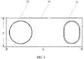
- the infrared sensor includes a strip-shaped packaging shell 53, the transmit end 51 is arranged at one end of the strip-shaped packaging shell 53, and the receive end 52 is arranged at the other end of the strip-shaped packaging shell 53.
- FIG. 3 is a schematic structural diagram of an infrared sensor according to an embodiment of this disclosure. It can be seen in FIG. 3 that X represents a long side of the infrared sensor, and Y represents a short side of the infrared sensor. A sensing area inside the infrared sensor is arranged horizontally, that is, arranged in an X direction. The strip-shaped packaging shell 53 is made into a thin and long shape to shorten Y as much as possible. This design not only ensures small stacking space in a Y direction, but also maintains sensitivity of the infrared sensor itself. A circle ring in FIG. 3 represents the receive end 52 of the infrared sensor, and an oval ring represents the transmit end 51 of the infrared sensor.
- a mobile terminal includes a cover plate 1, a display screen 2, a middle frame 3, an edge frame 4, and a photosensitive device 5.
- the cover plate 1 is fixedly connected to the edge frame 4, the display screen 2 is located between the cover plate 1 and the middle frame 3, a first gap is provided between the display screen 2 and the edge frame 4, a second gap is provided between the middle frame 3 and the edge frame 4, and the first gap and the second gap are connected to form an optical channel for the photosensitive device 5.
- the photosensitive device 5 does not need to be arranged on the front side of the mobile terminal, so that a screen-to-body ratio of the mobile terminal can be increased.
Landscapes
- Engineering & Computer Science (AREA)
- Signal Processing (AREA)
- Telephone Set Structure (AREA)
- Geophysics And Detection Of Objects (AREA)
Abstract
Description
- This application claims priority to Chinese Patent Application No.
201810426294.2, filed in China on May 7, 2018 - This disclosure relates to the field of communications technologies, and in particular, to a mobile terminal.
- With rapid development of mobile terminals, mobile terminals have become an indispensable tool in people's lives, and have brought great convenience to all aspects of users' lives. In the related art, there are some photosensitive devices, such as an infrared sensor or a photosensitive sensor, on a mobile terminal, and different photosensitive devices can implement different functions.
- However, a photosensitive device of the mobile terminal in the related art is generally arranged on the front side of the mobile terminal, which limits a screen-to-body ratio of the whole terminal, resulting in a relatively low screen-to-body ratio of the mobile terminal.
- Embodiments of this disclosure provide a mobile terminal, to resolve a problem of a relatively low screen-to-body ratio of the mobile terminal because a photosensitive device of the mobile terminal is generally arranged on the front side of the mobile terminal.
- To resolve the foregoing technical problem, this disclosure is implemented as follows: A mobile terminal includes a cover plate, a display screen, a middle frame, an edge frame, and a photosensitive device, where the cover plate is fixedly connected to the edge frame, the display screen is located between the cover plate and the middle frame, a first gap is provided between the display screen and the edge frame, a second gap is provided between the middle frame and the edge frame, and the first gap and the second gap are connected to form an optical channel for the photosensitive device.
- In this way, due to existence of the optical channel, the photosensitive device does not need to be arranged on the front side of the mobile terminal, so that the screen-to-body ratio of the mobile terminal can be increased.
- To describe the technical solutions in the embodiments of this disclosure more clearly, the following briefly describes the accompanying drawings required for describing the embodiments of this disclosure. Apparently, the accompanying drawings in the following descriptions show merely some embodiments of this disclosure, and a person of ordinary skill in the art may derive other drawings from these accompanying drawings without creative efforts.
-
FIG. 1 is a schematic structural diagram of a mobile terminal according to an embodiment of this disclosure; -
FIG. 2 is a schematic diagram of a connection between a circuit board and a main board according to an embodiment of this disclosure; and -
FIG. 3 is a schematic structural diagram of an infrared sensor according to an embodiment of this disclosure. - The following clearly and completely describes the technical solutions in the embodiments of this disclosure with reference to the accompanying drawings in the embodiments of this disclosure. Apparently, the described embodiments are some rather than all of the embodiments of this disclosure. All other embodiments obtained by a person of ordinary skill in the art based on the embodiments of this disclosure without creative efforts shall fall within the protection scope of this disclosure.
-
FIG. 1 is a schematic structural diagram of a mobile terminal according to an embodiment of this disclosure. As shown inFIG.1 , the mobile terminal includes acover plate 1, adisplay screen 2, amiddle frame 3, anedge frame 4, and aphotosensitive device 5. Thecover plate 1 is fixedly connected to theedge frame 4, thedisplay screen 2 is located between thecover plate 1 and themiddle frame 3, a first gap is provided between thedisplay screen 2 and theedge frame 4, a second gap is provided between themiddle frame 3 and theedge frame 4, and the first gap and the second gap are connected to form an optical channel for thephotosensitive device 5. - In this embodiment, the mobile terminal may further include a
circuit board 6 connected to the photosensitive device and abattery cover 7 connected to the edge frame. The mobile terminal may use thecircuit board 6 to control some internal components of the mobile terminal, and use thebattery cover 7 to enclose the internal components. Thecover plate 1 may be a glass cover plate, or may be a cover plate made of another synthetic material, or the like. Thedisplay screen 2 may be a liquid crystal display screen, or may be a display screen made of a crystal diode. Materials of themiddle frame 3 and theedge frame 4 may be metal, or may be some other synthetic materials, or the like. Thephotosensitive device 5 may be an infrared sensor, or may be a photosensitive sensor, or the like. Certainly, thephotosensitive device 5 may alternatively be another photosensitive device. This is not limited in this embodiment of this disclosure. - In this embodiment, the first gap is provided between the
display screen 2 and theedge frame 4, the second gap is provided between themiddle frame 3 and theedge frame 4, and the first gap and the second gap are connected to form an optical channel for thephotosensitive device 5. The first gap and the second gap are both assembly gaps, that is, structural gaps between the display screen, the middle frame, and the edge frame. In this way, light can reach thephotosensitive device 5 through the optical channel, so that thephotosensitive device 5 can receive the light, and thephotosensitive device 5 can also send a signal outward through the optical channel. - In the related art, it is necessary to set up special assembly space for the
photosensitive device 5 on a black border of the mobile terminal, which affects a screen-to-body ratio of the mobile terminal and makes it impossible to increase the screen-to-body ratio of the mobile terminal. However, in this embodiment, through a stacking design, a structural assembly gap (including the first gap and the second gap) is used as the optical channel of thephotosensitive device 5, avoiding occupying visual space that is occupied in a longitudinal direction of the mobile terminal in the related art, so that the mobile terminal can have a relatively high screen-to-body ratio. - In this embodiment of this disclosure, the foregoing mobile terminal may be a mobile phone, a tablet computer (Tablet Personal Computer), a laptop computer (Laptop Computer), a personal digital assistant (personal digital assistant, PDA), a mobile internet device (Mobile Internet Device, MID), a wearable device (Wearable Device), or the like.
- Optionally, the
photosensitive device 5 is arranged in the second gap. - In this implementation, the
photosensitive device 5 is arranged in the second gap, so that there is no need to set up independent assembly space for thephotosensitive device 5 on a black border of the mobile terminal, and only a structural assembly gap is required to achieve a relatively high screen-to-body ratio for the mobile terminal. - Optionally, the
photosensitive device 5 is an infrared sensor, a transmitend 51 and a receiveend 52 of the infrared sensor face thecover plate 1, and an infrared ray emitted by the infrared sensor may be emitted out of thecover plate 1 through the optical channel. - In this implementation, the
photosensitive device 5 is the infrared sensor, so that the infrared sensor can also be designed to detect a distance when the mobile terminal has a high screen-to-body ratio. The transmitend 51 and the receiveend 52 of the infrared sensor face thecover plate 1, and the emitted infrared ray may be emitted out of thecover plate 1 through the optical channel. When the infrared ray emitted by the transmitend 51 encounters an obstacle, the infrared ray can be reflected back and be received by the receiveend 52. In this way, the distance is detected. - Optionally, the
edge frame 4 is provided with a first step structure, thecover plate 1 is bonded to the first step structure through anadhesive layer 8, and theadhesive layer 8 includes a first side and a second side that are arranged oppositely, where the second side is a side close to thedisplay screen 2, and the first gap is located between the second side and thedisplay screen 2. - In this implementation, the
edge frame 4 is provided with the first step structure, so that thecover plate 1 can be arranged on the first step structure, and thecover plate 1 can be well accommodated. Thecover plate 1 is bonded to the first step structure through theadhesive layer 8, and thecover plate 1 can be well fixed on the first step structure. When being damaged, thecover plate 1 can be replaced easily. - Optionally, the mobile terminal further includes the
circuit board 6, the infrared sensor is electrically connected to thecircuit board 6, and thecircuit board 6 is fixedly connected to themiddle frame 3 and theedge frame 4. - In this implementation, the
circuit board 6 may be a common circuit board, may be a flexible circuit board, or may be a reinforcing board of a flexible circuit board, or the like. The infrared sensor is electrically connected to thecircuit board 6 to ensure that the infrared sensor can work well. Thecircuit board 6 may be fixedly connected, bonded, or connected by small screws, to themiddle frame 3 and theedge frame 4. - Optionally, the
edge frame 4 is provided with a second step structure, thecircuit board 6 is fixedly connected to the second step structure, and thecircuit board 6 is fixedly connected to a side, facing away from thedisplay screen 2, of themiddle frame 3. - In this implementation, the
edge frame 4 is provided with the second step structure, thecircuit board 6 is fixedly connected to the second step structure, and thecircuit board 6 is fixedly connected to the side, facing away from thedisplay screen 2, of themiddle frame 3, so that thecircuit board 6 can be well fixed to themiddle frame 3 and theedge frame 4. Certainly, to better fasten thecircuit board 6, a side of themiddle frame 3 that is fixedly connected to thecircuit board 6 and a side of theedge frame 4 that is fixedly connected to the circuit board may be on one plane, so that thecircuit board 6 can be fastened more firmly. - Optionally, the infrared sensor is welded to the
circuit board 6, and thecircuit board 6 is electrically connected to amain board 9. - In this implementation, the infrared sensor is welded to the
circuit board 6, so that the infrared sensor can be well fastened to thecircuit board 6 and is not prone to loose due to some vibrations of the mobile terminal, thereby ensuring measurement accuracy of the infrared sensor. - In this implementation, the
circuit board 6 is electrically connected to themain board 9, and the infrared sensor is electrically connected to thecircuit board 6, so that themain board 9 remains connected to the infrared sensor, to further control the infrared sensor. - Optionally, the
circuit board 6 is electrically connected to themain board 9 through aconnector 10 or an elastic sheet. - In this implementation, the
circuit board 6 is electrically connected to themain board 9 through theconnector 10 or the elastic sheet, and thecircuit board 6, themain board 9, and the infrared sensor remain connected to each other, so that the infrared sensor can be controlled through themain board 9. Theconnector 10 may be a board-to-board connector, or may be a zero insertion force connector, or the like. - For better understanding of the electrical connection between the
circuit board 6 and themain board 9, reference may be made toFIG. 2. FIG. 2 is a schematic diagram of a connection between a circuit board and a main board according to an embodiment of this disclosure. It can be seen fromFIG. 2 that thecircuit board 6 is connected to themain board 9 through the connector 10 (which is a board-to-board connector in this case), and thecircuit board 6, themain board 9, and the infrared sensor remain connected to each other, so that the infrared sensor can be controlled through themain board 9. - Optionally, a width of the second gap is greater than or equal to a width of the first gap.
- In this implementation, because the
photosensitive device 5 is arranged in the second gap, setting the width of the second gap to a relatively large value can better accommodate thephotosensitive device 5, such as the infrared sensor. The first gap is a gap between thedisplay screen 2 and theedge frame 4. Setting the width of the first gap to a relatively small value can enhance visual appeal without affecting a full-screen display design, so that the mobile terminal can have a relatively high screen-to-body ratio. Optionally, the width of the first gap may be set between 0.3 mm and 1 mm to achieve a visual effect of full-screen display. - Optionally, the optical channel is provided with a light absorbing layer.
- In this implementation, the optical channel is provided with the light absorbing layer that absorbs light. Black ink can be sprayed on an inner wall of the optical channel, or a black material can be directly used as an inner wall of the optical channel, so that the optical channel is provided with the light absorbing layer that absorbs light. In this way, strong reflection in the optical channel can be prevented from affecting performance of the photosensitive device 5 (for example, the infrared sensor).
- Optionally, the infrared sensor includes a strip-shaped
packaging shell 53, the transmitend 51 is arranged at one end of the strip-shapedpackaging shell 53, and the receiveend 52 is arranged at the other end of the strip-shapedpackaging shell 53. - In this implementation, for better understanding of the foregoing structure, reference may be made to
FIG. 3. FIG. 3 is a schematic structural diagram of an infrared sensor according to an embodiment of this disclosure. It can be seen inFIG. 3 that X represents a long side of the infrared sensor, and Y represents a short side of the infrared sensor. A sensing area inside the infrared sensor is arranged horizontally, that is, arranged in an X direction. The strip-shapedpackaging shell 53 is made into a thin and long shape to shorten Y as much as possible. This design not only ensures small stacking space in a Y direction, but also maintains sensitivity of the infrared sensor itself. A circle ring inFIG. 3 represents the receiveend 52 of the infrared sensor, and an oval ring represents the transmitend 51 of the infrared sensor. - A mobile terminal according to an embodiment of this disclosure includes a
cover plate 1, adisplay screen 2, amiddle frame 3, anedge frame 4, and aphotosensitive device 5. Thecover plate 1 is fixedly connected to theedge frame 4, thedisplay screen 2 is located between thecover plate 1 and themiddle frame 3, a first gap is provided between thedisplay screen 2 and theedge frame 4, a second gap is provided between themiddle frame 3 and theedge frame 4, and the first gap and the second gap are connected to form an optical channel for thephotosensitive device 5. In this way, due to existence of the optical channel, thephotosensitive device 5 does not need to be arranged on the front side of the mobile terminal, so that a screen-to-body ratio of the mobile terminal can be increased. - It should be noted that the terms "include", "comprise", or any of their variants are intended to cover a non-exclusive inclusion, such that a process, a method, an article, or an apparatus that includes a list of elements not only includes those elements but also includes other elements that are not expressly listed, or further includes elements inherent to such process, method, article, or apparatus. In absence of more constraints, an element preceded by "includes a..." does not preclude the existence of other identical elements in the process, method, article, or apparatus that includes the element.
- The embodiments of this disclosure are described above with reference to the accompanying drawings, but this disclosure is not limited to the foregoing implementations. The foregoing implementations are only illustrative rather than restrictive. Inspired by this disclosure, a person of ordinary skill in the art can still derive many variations without departing from the essence of this disclosure and the protection scope of the claims. All these variations shall fall within the protection of this disclosure.
Claims (12)
- A mobile terminal, comprising a cover plate, a display screen, a middle frame, an edge frame, and a photosensitive device, wherein the cover plate is fixedly connected to the edge frame, the display screen is located between the cover plate and the middle frame, a first gap is provided between the display screen and the edge frame, a second gap is provided between the middle frame and the edge frame, and the first gap and the second gap are connected to form an optical channel for the photosensitive device.
- The mobile terminal according to claim 1, wherein the photosensitive device is arranged in the second gap.
- The mobile terminal according to claim 2, wherein the photosensitive device is an infrared sensor, a transmit end and a receive end of the infrared sensor face the cover plate, and an infrared ray emitted by the infrared sensor is emitted out of the cover plate through the optical channel.
- The mobile terminal according to claim 3, wherein the edge frame is provided with a first step structure, the cover plate is bonded to the first step structure through an adhesive layer, and the adhesive layer comprises a first side and a second side that are arranged oppositely, wherein the second side is a side close to the display screen, and the first gap is located between the second side and the display screen.
- The mobile terminal according to claim 3, wherein the mobile terminal further comprises a circuit board, the infrared sensor is electrically connected to the circuit board, and the circuit board is fixedly connected to the middle frame and the edge frame.
- The mobile terminal according to claim 5, wherein the edge frame is provided with a second step structure, the circuit board is fixedly connected to the second step structure, and the circuit board is fixedly connected to a side, facing away from the display screen, of the middle frame.
- The mobile terminal according to claim 5, wherein the infrared sensor is welded to the circuit board, and the circuit board is electrically connected to a main board.
- The mobile terminal according to claim 7, wherein the circuit board is electrically connected to the main board through a connector or an elastic sheet.
- The mobile terminal according to any one of claims 2 to 8, wherein an inner wall of the optical channel is provided with a light absorbing layer.
- The mobile terminal according to claim 9, wherein the light absorbing layer is made of black ink, or the optical channel is made of a black material.
- The mobile terminal according to any one of claims 3 to 8, wherein the infrared sensor comprises a strip-shaped packaging shell, the transmit end is arranged at one end of the strip-shaped packaging shell, and the receive end is arranged at the other end of the strip-shaped packaging shell.
- The mobile terminal according to claim 11, wherein a sensing area inside the infrared sensor is arranged along a longitudinal direction of the strip-shaped packaging shell.
Applications Claiming Priority (2)
| Application Number | Priority Date | Filing Date | Title |
|---|---|---|---|
| CN201810426294.2A CN108600460B (en) | 2018-05-07 | 2018-05-07 | Mobile terminal |
| PCT/CN2019/085815 WO2019214602A1 (en) | 2018-05-07 | 2019-05-07 | Mobile terminal |
Publications (3)
| Publication Number | Publication Date |
|---|---|
| EP3817343A1 true EP3817343A1 (en) | 2021-05-05 |
| EP3817343A4 EP3817343A4 (en) | 2021-06-23 |
| EP3817343B1 EP3817343B1 (en) | 2023-12-13 |
Family
ID=63619801
Family Applications (1)
| Application Number | Title | Priority Date | Filing Date |
|---|---|---|---|
| EP19800361.8A Active EP3817343B1 (en) | 2018-05-07 | 2019-05-07 | Mobile terminal |
Country Status (5)
| Country | Link |
|---|---|
| US (1) | US11546452B2 (en) |
| EP (1) | EP3817343B1 (en) |
| CN (1) | CN108600460B (en) |
| ES (1) | ES2968934T3 (en) |
| WO (1) | WO2019214602A1 (en) |
Families Citing this family (4)
| Publication number | Priority date | Publication date | Assignee | Title |
|---|---|---|---|---|
| CN108600460B (en) * | 2018-05-07 | 2020-10-09 | 维沃移动通信有限公司 | Mobile terminal |
| CN108900667B (en) * | 2018-06-22 | 2021-01-22 | 维沃移动通信有限公司 | a mobile terminal |
| CN110839098B (en) * | 2019-11-11 | 2021-10-01 | 维沃移动通信有限公司 | A cover glass assembly and mobile terminal |
| CN114500869B (en) * | 2020-11-13 | 2024-04-05 | 荣耀终端有限公司 | Electronic equipment and under-screen light detection assembly |
Family Cites Families (21)
| Publication number | Priority date | Publication date | Assignee | Title |
|---|---|---|---|---|
| EP2073105A1 (en) * | 2007-12-19 | 2009-06-24 | Shu-Fen Li | Optical contact controlled medium display |
| KR101901610B1 (en) * | 2011-11-03 | 2018-09-28 | 엘지전자 주식회사 | Portable terminal |
| CN203070255U (en) * | 2012-12-05 | 2013-07-17 | 成都吉锐触摸技术股份有限公司 | Infrared touch screen |
| US10288476B2 (en) * | 2015-12-21 | 2019-05-14 | Apple Inc. | Ambient light sensor window coatings for electronic devices |
| CN105704268A (en) * | 2016-01-29 | 2016-06-22 | 华为技术有限公司 | Cover glass assembly |
| CN206226512U (en) * | 2016-11-08 | 2017-06-06 | 努比亚技术有限公司 | Mobile terminal |
| CN106500836B (en) * | 2016-12-08 | 2018-01-02 | 苏州聚晟太阳能科技股份有限公司 | A kind of optical sensor suitable for photovoltaic tracking |
| CN106850982B (en) * | 2017-01-20 | 2019-08-06 | Oppo广东移动通信有限公司 | Display state control method and device |
| CN106873879B (en) * | 2017-01-25 | 2019-10-29 | 维沃移动通信有限公司 | A kind of electronic equipment and put out screen processing method, device |
| CN110226320B (en) * | 2017-01-26 | 2021-01-12 | Lg电子株式会社 | Mobile terminal |
| CN106850898B (en) * | 2017-03-07 | 2020-02-14 | Oppo广东移动通信有限公司 | Mobile terminal |
| CN107122011A (en) | 2017-06-29 | 2017-09-01 | 北京小米移动软件有限公司 | Mobile device |
| CN107659688A (en) * | 2017-10-31 | 2018-02-02 | 努比亚技术有限公司 | A kind of method, screen mounting structure and mobile terminal for increasing front panel accounting |
| WO2019093640A1 (en) * | 2017-11-10 | 2019-05-16 | Lg Electronics Inc. | Display device |
| CN107909922B (en) | 2017-11-16 | 2019-10-15 | 维沃移动通信有限公司 | A kind of mobile terminal |
| CN107945661B (en) * | 2017-11-22 | 2019-11-15 | 维沃移动通信有限公司 | a terminal device |
| CN107770315B (en) * | 2017-11-29 | 2025-07-15 | 北京小米移动软件有限公司 | Mobile Terminal |
| WO2019184561A1 (en) * | 2018-03-31 | 2019-10-03 | Guangdong Oppo Mobile Telecommunications Corp., Ltd. | Electronic device |
| CN108600460B (en) * | 2018-05-07 | 2020-10-09 | 维沃移动通信有限公司 | Mobile terminal |
| CN208721790U (en) * | 2018-05-29 | 2019-04-09 | 维沃移动通信有限公司 | A kind of terminal device |
| CN109101083B (en) * | 2018-08-23 | 2020-05-29 | 维沃移动通信有限公司 | Terminal |
-
2018
- 2018-05-07 CN CN201810426294.2A patent/CN108600460B/en active Active
-
2019
- 2019-05-07 WO PCT/CN2019/085815 patent/WO2019214602A1/en not_active Ceased
- 2019-05-07 EP EP19800361.8A patent/EP3817343B1/en active Active
- 2019-05-07 ES ES19800361T patent/ES2968934T3/en active Active
-
2020
- 2020-11-06 US US17/092,092 patent/US11546452B2/en active Active
Also Published As
| Publication number | Publication date |
|---|---|
| WO2019214602A1 (en) | 2019-11-14 |
| EP3817343B1 (en) | 2023-12-13 |
| US11546452B2 (en) | 2023-01-03 |
| US20210058501A1 (en) | 2021-02-25 |
| EP3817343A4 (en) | 2021-06-23 |
| CN108600460B (en) | 2020-10-09 |
| ES2968934T3 (en) | 2024-05-14 |
| CN108600460A (en) | 2018-09-28 |
Similar Documents
| Publication | Publication Date | Title |
|---|---|---|
| US11546452B2 (en) | Mobile terminal | |
| CN207530869U (en) | A kind of mobile terminal | |
| US9798401B2 (en) | Touch screen, method of manufacture the same, and mobile terminal having the same | |
| CN107979663B (en) | Sensor components, display components and electronic equipment | |
| CN107241468B (en) | Display device and mobile terminal | |
| EP3671721A1 (en) | Electronic device | |
| EP3484131B1 (en) | Camera device of a mobile terminal | |
| JP7176007B2 (en) | mobile computer | |
| US11455018B2 (en) | Optical proximity sensor component comprising light guide | |
| US9367155B2 (en) | Touch panel assembly and electronic device | |
| US20190141220A1 (en) | Camera device, bracket and mobile terminal using same | |
| KR100897973B1 (en) | Signal applying unit of window integrated touch screen | |
| CN110581904A (en) | Control method, control device, electronic device and storage medium | |
| CN110174961A (en) | Mobile terminal | |
| CN112437899B (en) | Electronic equipment and light guide parts | |
| CN109769052B (en) | Electronic equipment | |
| WO2020014819A1 (en) | Electronic device | |
| US20150077655A1 (en) | Electronic device without front case frame | |
| EP3820122B1 (en) | Electronic device | |
| US9319498B2 (en) | Portable electronic device | |
| CN108989566A (en) | Control method, electronic device, and computer-readable storage medium | |
| CN110138943A (en) | Electronic equipment and control method of camera | |
| CN209964155U (en) | Electronic device | |
| CN108810208B (en) | Display screen assembly and electronic equipment | |
| US10393600B2 (en) | Portable electronic device and sensing method thereof |
Legal Events
| Date | Code | Title | Description |
|---|---|---|---|
| STAA | Information on the status of an ep patent application or granted ep patent |
Free format text: STATUS: THE INTERNATIONAL PUBLICATION HAS BEEN MADE |
|
| PUAI | Public reference made under article 153(3) epc to a published international application that has entered the european phase |
Free format text: ORIGINAL CODE: 0009012 |
|
| STAA | Information on the status of an ep patent application or granted ep patent |
Free format text: STATUS: REQUEST FOR EXAMINATION WAS MADE |
|
| 17P | Request for examination filed |
Effective date: 20201201 |
|
| AK | Designated contracting states |
Kind code of ref document: A1 Designated state(s): AL AT BE BG CH CY CZ DE DK EE ES FI FR GB GR HR HU IE IS IT LI LT LU LV MC MK MT NL NO PL PT RO RS SE SI SK SM TR |
|
| A4 | Supplementary search report drawn up and despatched |
Effective date: 20210520 |
|
| RIC1 | Information provided on ipc code assigned before grant |
Ipc: H04M 1/02 20060101AFI20210514BHEP |
|
| DAV | Request for validation of the european patent (deleted) | ||
| DAX | Request for extension of the european patent (deleted) | ||
| STAA | Information on the status of an ep patent application or granted ep patent |
Free format text: STATUS: EXAMINATION IS IN PROGRESS |
|
| 17Q | First examination report despatched |
Effective date: 20220831 |
|
| GRAP | Despatch of communication of intention to grant a patent |
Free format text: ORIGINAL CODE: EPIDOSNIGR1 |
|
| STAA | Information on the status of an ep patent application or granted ep patent |
Free format text: STATUS: GRANT OF PATENT IS INTENDED |
|
| INTG | Intention to grant announced |
Effective date: 20230814 |
|
| GRAS | Grant fee paid |
Free format text: ORIGINAL CODE: EPIDOSNIGR3 |
|
| GRAA | (expected) grant |
Free format text: ORIGINAL CODE: 0009210 |
|
| STAA | Information on the status of an ep patent application or granted ep patent |
Free format text: STATUS: THE PATENT HAS BEEN GRANTED |
|
| AK | Designated contracting states |
Kind code of ref document: B1 Designated state(s): AL AT BE BG CH CY CZ DE DK EE ES FI FR GB GR HR HU IE IS IT LI LT LU LV MC MK MT NL NO PL PT RO RS SE SI SK SM TR |
|
| REG | Reference to a national code |
Ref country code: GB Ref legal event code: FG4D |
|
| REG | Reference to a national code |
Ref country code: CH Ref legal event code: EP |
|
| REG | Reference to a national code |
Ref country code: DE Ref legal event code: R096 Ref document number: 602019043306 Country of ref document: DE |
|
| REG | Reference to a national code |
Ref country code: IE Ref legal event code: FG4D |
|
| REG | Reference to a national code |
Ref country code: NL Ref legal event code: FP |
|
| PG25 | Lapsed in a contracting state [announced via postgrant information from national office to epo] |
Ref country code: GR Free format text: LAPSE BECAUSE OF FAILURE TO SUBMIT A TRANSLATION OF THE DESCRIPTION OR TO PAY THE FEE WITHIN THE PRESCRIBED TIME-LIMIT Effective date: 20240314 |
|
| REG | Reference to a national code |
Ref country code: LT Ref legal event code: MG9D |
|
| PG25 | Lapsed in a contracting state [announced via postgrant information from national office to epo] |
Ref country code: LT Free format text: LAPSE BECAUSE OF FAILURE TO SUBMIT A TRANSLATION OF THE DESCRIPTION OR TO PAY THE FEE WITHIN THE PRESCRIBED TIME-LIMIT Effective date: 20231213 |
|
| PG25 | Lapsed in a contracting state [announced via postgrant information from national office to epo] |
Ref country code: LT Free format text: LAPSE BECAUSE OF FAILURE TO SUBMIT A TRANSLATION OF THE DESCRIPTION OR TO PAY THE FEE WITHIN THE PRESCRIBED TIME-LIMIT Effective date: 20231213 Ref country code: GR Free format text: LAPSE BECAUSE OF FAILURE TO SUBMIT A TRANSLATION OF THE DESCRIPTION OR TO PAY THE FEE WITHIN THE PRESCRIBED TIME-LIMIT Effective date: 20240314 Ref country code: BG Free format text: LAPSE BECAUSE OF FAILURE TO SUBMIT A TRANSLATION OF THE DESCRIPTION OR TO PAY THE FEE WITHIN THE PRESCRIBED TIME-LIMIT Effective date: 20240313 |
|
| REG | Reference to a national code |
Ref country code: ES Ref legal event code: FG2A Ref document number: 2968934 Country of ref document: ES Kind code of ref document: T3 Effective date: 20240514 |
|
| REG | Reference to a national code |
Ref country code: AT Ref legal event code: MK05 Ref document number: 1641459 Country of ref document: AT Kind code of ref document: T Effective date: 20231213 |
|
| PG25 | Lapsed in a contracting state [announced via postgrant information from national office to epo] |
Ref country code: SE Free format text: LAPSE BECAUSE OF FAILURE TO SUBMIT A TRANSLATION OF THE DESCRIPTION OR TO PAY THE FEE WITHIN THE PRESCRIBED TIME-LIMIT Effective date: 20231213 Ref country code: RS Free format text: LAPSE BECAUSE OF FAILURE TO SUBMIT A TRANSLATION OF THE DESCRIPTION OR TO PAY THE FEE WITHIN THE PRESCRIBED TIME-LIMIT Effective date: 20231213 Ref country code: NO Free format text: LAPSE BECAUSE OF FAILURE TO SUBMIT A TRANSLATION OF THE DESCRIPTION OR TO PAY THE FEE WITHIN THE PRESCRIBED TIME-LIMIT Effective date: 20240313 Ref country code: LV Free format text: LAPSE BECAUSE OF FAILURE TO SUBMIT A TRANSLATION OF THE DESCRIPTION OR TO PAY THE FEE WITHIN THE PRESCRIBED TIME-LIMIT Effective date: 20231213 Ref country code: HR Free format text: LAPSE BECAUSE OF FAILURE TO SUBMIT A TRANSLATION OF THE DESCRIPTION OR TO PAY THE FEE WITHIN THE PRESCRIBED TIME-LIMIT Effective date: 20231213 |
|
| PG25 | Lapsed in a contracting state [announced via postgrant information from national office to epo] |
Ref country code: IS Free format text: LAPSE BECAUSE OF FAILURE TO SUBMIT A TRANSLATION OF THE DESCRIPTION OR TO PAY THE FEE WITHIN THE PRESCRIBED TIME-LIMIT Effective date: 20240413 |
|
| PG25 | Lapsed in a contracting state [announced via postgrant information from national office to epo] |
Ref country code: AT Free format text: LAPSE BECAUSE OF FAILURE TO SUBMIT A TRANSLATION OF THE DESCRIPTION OR TO PAY THE FEE WITHIN THE PRESCRIBED TIME-LIMIT Effective date: 20231213 Ref country code: CZ Free format text: LAPSE BECAUSE OF FAILURE TO SUBMIT A TRANSLATION OF THE DESCRIPTION OR TO PAY THE FEE WITHIN THE PRESCRIBED TIME-LIMIT Effective date: 20231213 |
|
| PG25 | Lapsed in a contracting state [announced via postgrant information from national office to epo] |
Ref country code: SK Free format text: LAPSE BECAUSE OF FAILURE TO SUBMIT A TRANSLATION OF THE DESCRIPTION OR TO PAY THE FEE WITHIN THE PRESCRIBED TIME-LIMIT Effective date: 20231213 |
|
| PG25 | Lapsed in a contracting state [announced via postgrant information from national office to epo] |
Ref country code: SM Free format text: LAPSE BECAUSE OF FAILURE TO SUBMIT A TRANSLATION OF THE DESCRIPTION OR TO PAY THE FEE WITHIN THE PRESCRIBED TIME-LIMIT Effective date: 20231213 Ref country code: SK Free format text: LAPSE BECAUSE OF FAILURE TO SUBMIT A TRANSLATION OF THE DESCRIPTION OR TO PAY THE FEE WITHIN THE PRESCRIBED TIME-LIMIT Effective date: 20231213 Ref country code: RO Free format text: LAPSE BECAUSE OF FAILURE TO SUBMIT A TRANSLATION OF THE DESCRIPTION OR TO PAY THE FEE WITHIN THE PRESCRIBED TIME-LIMIT Effective date: 20231213 Ref country code: IS Free format text: LAPSE BECAUSE OF FAILURE TO SUBMIT A TRANSLATION OF THE DESCRIPTION OR TO PAY THE FEE WITHIN THE PRESCRIBED TIME-LIMIT Effective date: 20240413 Ref country code: EE Free format text: LAPSE BECAUSE OF FAILURE TO SUBMIT A TRANSLATION OF THE DESCRIPTION OR TO PAY THE FEE WITHIN THE PRESCRIBED TIME-LIMIT Effective date: 20231213 Ref country code: CZ Free format text: LAPSE BECAUSE OF FAILURE TO SUBMIT A TRANSLATION OF THE DESCRIPTION OR TO PAY THE FEE WITHIN THE PRESCRIBED TIME-LIMIT Effective date: 20231213 Ref country code: AT Free format text: LAPSE BECAUSE OF FAILURE TO SUBMIT A TRANSLATION OF THE DESCRIPTION OR TO PAY THE FEE WITHIN THE PRESCRIBED TIME-LIMIT Effective date: 20231213 |
|
| PG25 | Lapsed in a contracting state [announced via postgrant information from national office to epo] |
Ref country code: PT Free format text: LAPSE BECAUSE OF FAILURE TO SUBMIT A TRANSLATION OF THE DESCRIPTION OR TO PAY THE FEE WITHIN THE PRESCRIBED TIME-LIMIT Effective date: 20240415 Ref country code: PL Free format text: LAPSE BECAUSE OF FAILURE TO SUBMIT A TRANSLATION OF THE DESCRIPTION OR TO PAY THE FEE WITHIN THE PRESCRIBED TIME-LIMIT Effective date: 20231213 |
|
| PG25 | Lapsed in a contracting state [announced via postgrant information from national office to epo] |
Ref country code: PT Free format text: LAPSE BECAUSE OF FAILURE TO SUBMIT A TRANSLATION OF THE DESCRIPTION OR TO PAY THE FEE WITHIN THE PRESCRIBED TIME-LIMIT Effective date: 20240415 Ref country code: PL Free format text: LAPSE BECAUSE OF FAILURE TO SUBMIT A TRANSLATION OF THE DESCRIPTION OR TO PAY THE FEE WITHIN THE PRESCRIBED TIME-LIMIT Effective date: 20231213 |
|
| REG | Reference to a national code |
Ref country code: DE Ref legal event code: R097 Ref document number: 602019043306 Country of ref document: DE |
|
| PG25 | Lapsed in a contracting state [announced via postgrant information from national office to epo] |
Ref country code: DK Free format text: LAPSE BECAUSE OF FAILURE TO SUBMIT A TRANSLATION OF THE DESCRIPTION OR TO PAY THE FEE WITHIN THE PRESCRIBED TIME-LIMIT Effective date: 20231213 |
|
| PLBE | No opposition filed within time limit |
Free format text: ORIGINAL CODE: 0009261 |
|
| STAA | Information on the status of an ep patent application or granted ep patent |
Free format text: STATUS: NO OPPOSITION FILED WITHIN TIME LIMIT |
|
| PG25 | Lapsed in a contracting state [announced via postgrant information from national office to epo] |
Ref country code: SI Free format text: LAPSE BECAUSE OF FAILURE TO SUBMIT A TRANSLATION OF THE DESCRIPTION OR TO PAY THE FEE WITHIN THE PRESCRIBED TIME-LIMIT Effective date: 20231213 |
|
| PG25 | Lapsed in a contracting state [announced via postgrant information from national office to epo] |
Ref country code: SI Free format text: LAPSE BECAUSE OF FAILURE TO SUBMIT A TRANSLATION OF THE DESCRIPTION OR TO PAY THE FEE WITHIN THE PRESCRIBED TIME-LIMIT Effective date: 20231213 Ref country code: DK Free format text: LAPSE BECAUSE OF FAILURE TO SUBMIT A TRANSLATION OF THE DESCRIPTION OR TO PAY THE FEE WITHIN THE PRESCRIBED TIME-LIMIT Effective date: 20231213 |
|
| 26N | No opposition filed |
Effective date: 20240916 |
|
| REG | Reference to a national code |
Ref country code: CH Ref legal event code: PL |
|
| PG25 | Lapsed in a contracting state [announced via postgrant information from national office to epo] |
Ref country code: MC Free format text: LAPSE BECAUSE OF FAILURE TO SUBMIT A TRANSLATION OF THE DESCRIPTION OR TO PAY THE FEE WITHIN THE PRESCRIBED TIME-LIMIT Effective date: 20231213 |
|
| PG25 | Lapsed in a contracting state [announced via postgrant information from national office to epo] |
Ref country code: LU Free format text: LAPSE BECAUSE OF NON-PAYMENT OF DUE FEES Effective date: 20240507 |
|
| PG25 | Lapsed in a contracting state [announced via postgrant information from national office to epo] |
Ref country code: MC Free format text: LAPSE BECAUSE OF FAILURE TO SUBMIT A TRANSLATION OF THE DESCRIPTION OR TO PAY THE FEE WITHIN THE PRESCRIBED TIME-LIMIT Effective date: 20231213 Ref country code: LU Free format text: LAPSE BECAUSE OF NON-PAYMENT OF DUE FEES Effective date: 20240507 Ref country code: CH Free format text: LAPSE BECAUSE OF NON-PAYMENT OF DUE FEES Effective date: 20240531 |
|
| REG | Reference to a national code |
Ref country code: BE Ref legal event code: MM Effective date: 20240531 |
|
| PG25 | Lapsed in a contracting state [announced via postgrant information from national office to epo] |
Ref country code: IE Free format text: LAPSE BECAUSE OF NON-PAYMENT OF DUE FEES Effective date: 20240507 |
|
| PG25 | Lapsed in a contracting state [announced via postgrant information from national office to epo] |
Ref country code: BE Free format text: LAPSE BECAUSE OF NON-PAYMENT OF DUE FEES Effective date: 20240531 |
|
| PGFP | Annual fee paid to national office [announced via postgrant information from national office to epo] |
Ref country code: NL Payment date: 20250409 Year of fee payment: 7 |
|
| PGFP | Annual fee paid to national office [announced via postgrant information from national office to epo] |
Ref country code: DE Payment date: 20250402 Year of fee payment: 7 |
|
| PGFP | Annual fee paid to national office [announced via postgrant information from national office to epo] |
Ref country code: ES Payment date: 20250606 Year of fee payment: 7 |
|
| PGFP | Annual fee paid to national office [announced via postgrant information from national office to epo] |
Ref country code: IT Payment date: 20250422 Year of fee payment: 7 |
|
| PGFP | Annual fee paid to national office [announced via postgrant information from national office to epo] |
Ref country code: FR Payment date: 20250401 Year of fee payment: 7 |
|
| PG25 | Lapsed in a contracting state [announced via postgrant information from national office to epo] |
Ref country code: CY Free format text: LAPSE BECAUSE OF FAILURE TO SUBMIT A TRANSLATION OF THE DESCRIPTION OR TO PAY THE FEE WITHIN THE PRESCRIBED TIME-LIMIT; INVALID AB INITIO Effective date: 20190507 |
|
| PG25 | Lapsed in a contracting state [announced via postgrant information from national office to epo] |
Ref country code: HU Free format text: LAPSE BECAUSE OF FAILURE TO SUBMIT A TRANSLATION OF THE DESCRIPTION OR TO PAY THE FEE WITHIN THE PRESCRIBED TIME-LIMIT; INVALID AB INITIO Effective date: 20190507 |
|
| PG25 | Lapsed in a contracting state [announced via postgrant information from national office to epo] |
Ref country code: FI Free format text: LAPSE BECAUSE OF FAILURE TO SUBMIT A TRANSLATION OF THE DESCRIPTION OR TO PAY THE FEE WITHIN THE PRESCRIBED TIME-LIMIT Effective date: 20231213 |
|
| PGFP | Annual fee paid to national office [announced via postgrant information from national office to epo] |
Ref country code: GB Payment date: 20260324 Year of fee payment: 8 |