EP3817145A1 - Antenna unit, array antenna, and electronic device - Google Patents
Antenna unit, array antenna, and electronic device Download PDFInfo
- Publication number
- EP3817145A1 EP3817145A1 EP20159664.0A EP20159664A EP3817145A1 EP 3817145 A1 EP3817145 A1 EP 3817145A1 EP 20159664 A EP20159664 A EP 20159664A EP 3817145 A1 EP3817145 A1 EP 3817145A1
- Authority
- EP
- European Patent Office
- Prior art keywords
- layer
- feeder line
- dielectric layer
- antenna
- radiating
- Prior art date
- Legal status (The legal status is an assumption and is not a legal conclusion. Google has not performed a legal analysis and makes no representation as to the accuracy of the status listed.)
- Pending
Links
Images






Classifications
-
- H—ELECTRICITY
- H01—ELECTRIC ELEMENTS
- H01Q—ANTENNAS, i.e. RADIO AERIALS
- H01Q9/00—Electrically-short antennas having dimensions not more than twice the operating wavelength and consisting of conductive active radiating elements
- H01Q9/04—Resonant antennas
- H01Q9/0407—Substantially flat resonant element parallel to ground plane, e.g. patch antenna
- H01Q9/0414—Substantially flat resonant element parallel to ground plane, e.g. patch antenna in a stacked or folded configuration
-
- H—ELECTRICITY
- H01—ELECTRIC ELEMENTS
- H01Q—ANTENNAS, i.e. RADIO AERIALS
- H01Q9/00—Electrically-short antennas having dimensions not more than twice the operating wavelength and consisting of conductive active radiating elements
- H01Q9/04—Resonant antennas
- H01Q9/0407—Substantially flat resonant element parallel to ground plane, e.g. patch antenna
- H01Q9/045—Substantially flat resonant element parallel to ground plane, e.g. patch antenna with particular feeding means
- H01Q9/0457—Substantially flat resonant element parallel to ground plane, e.g. patch antenna with particular feeding means electromagnetically coupled to the feed line
-
- H—ELECTRICITY
- H01—ELECTRIC ELEMENTS
- H01Q—ANTENNAS, i.e. RADIO AERIALS
- H01Q1/00—Details of, or arrangements associated with, antennas
- H01Q1/36—Structural form of radiating elements, e.g. cone, spiral, umbrella; Particular materials used therewith
- H01Q1/38—Structural form of radiating elements, e.g. cone, spiral, umbrella; Particular materials used therewith formed by a conductive layer on an insulating support
-
- H—ELECTRICITY
- H01—ELECTRIC ELEMENTS
- H01Q—ANTENNAS, i.e. RADIO AERIALS
- H01Q1/00—Details of, or arrangements associated with, antennas
- H01Q1/12—Supports; Mounting means
- H01Q1/22—Supports; Mounting means by structural association with other equipment or articles
- H01Q1/24—Supports; Mounting means by structural association with other equipment or articles with receiving set
-
- H—ELECTRICITY
- H01—ELECTRIC ELEMENTS
- H01Q—ANTENNAS, i.e. RADIO AERIALS
- H01Q1/00—Details of, or arrangements associated with, antennas
- H01Q1/12—Supports; Mounting means
- H01Q1/22—Supports; Mounting means by structural association with other equipment or articles
- H01Q1/24—Supports; Mounting means by structural association with other equipment or articles with receiving set
- H01Q1/241—Supports; Mounting means by structural association with other equipment or articles with receiving set used in mobile communications, e.g. GSM
- H01Q1/242—Supports; Mounting means by structural association with other equipment or articles with receiving set used in mobile communications, e.g. GSM specially adapted for hand-held use
- H01Q1/243—Supports; Mounting means by structural association with other equipment or articles with receiving set used in mobile communications, e.g. GSM specially adapted for hand-held use with built-in antennas
-
- H—ELECTRICITY
- H01—ELECTRIC ELEMENTS
- H01Q—ANTENNAS, i.e. RADIO AERIALS
- H01Q1/00—Details of, or arrangements associated with, antennas
- H01Q1/36—Structural form of radiating elements, e.g. cone, spiral, umbrella; Particular materials used therewith
-
- H—ELECTRICITY
- H01—ELECTRIC ELEMENTS
- H01Q—ANTENNAS, i.e. RADIO AERIALS
- H01Q1/00—Details of, or arrangements associated with, antennas
- H01Q1/48—Earthing means; Earth screens; Counterpoises
-
- H—ELECTRICITY
- H01—ELECTRIC ELEMENTS
- H01Q—ANTENNAS, i.e. RADIO AERIALS
- H01Q1/00—Details of, or arrangements associated with, antennas
- H01Q1/50—Structural association of antennas with earthing switches, lead-in devices or lightning protectors
-
- H—ELECTRICITY
- H01—ELECTRIC ELEMENTS
- H01Q—ANTENNAS, i.e. RADIO AERIALS
- H01Q21/00—Antenna arrays or systems
-
- H—ELECTRICITY
- H01—ELECTRIC ELEMENTS
- H01Q—ANTENNAS, i.e. RADIO AERIALS
- H01Q21/00—Antenna arrays or systems
- H01Q21/0006—Particular feeding systems
- H01Q21/0075—Stripline fed arrays
-
- H—ELECTRICITY
- H01—ELECTRIC ELEMENTS
- H01Q—ANTENNAS, i.e. RADIO AERIALS
- H01Q5/00—Arrangements for simultaneous operation of antennas on two or more different wavebands, e.g. dual-band or multi-band arrangements
- H01Q5/30—Arrangements for providing operation on different wavebands
- H01Q5/307—Individual or coupled radiating elements, each element being fed in an unspecified way
-
- H—ELECTRICITY
- H01—ELECTRIC ELEMENTS
- H01Q—ANTENNAS, i.e. RADIO AERIALS
- H01Q9/00—Electrically-short antennas having dimensions not more than twice the operating wavelength and consisting of conductive active radiating elements
- H01Q9/04—Resonant antennas
-
- H—ELECTRICITY
- H01—ELECTRIC ELEMENTS
- H01Q—ANTENNAS, i.e. RADIO AERIALS
- H01Q9/00—Electrically-short antennas having dimensions not more than twice the operating wavelength and consisting of conductive active radiating elements
- H01Q9/04—Resonant antennas
- H01Q9/0407—Substantially flat resonant element parallel to ground plane, e.g. patch antenna
- H01Q9/0421—Substantially flat resonant element parallel to ground plane, e.g. patch antenna with a shorting wall or a shorting pin at one end of the element
-
- H—ELECTRICITY
- H01—ELECTRIC ELEMENTS
- H01Q—ANTENNAS, i.e. RADIO AERIALS
- H01Q9/00—Electrically-short antennas having dimensions not more than twice the operating wavelength and consisting of conductive active radiating elements
- H01Q9/04—Resonant antennas
- H01Q9/0407—Substantially flat resonant element parallel to ground plane, e.g. patch antenna
- H01Q9/045—Substantially flat resonant element parallel to ground plane, e.g. patch antenna with particular feeding means
Definitions
- the disclosure relates to the field of 5G communications, and more particularly, to an antenna unit, an array antenna, and an electronic device.
- antenna units of more and more electronic devices support 5G communication(s).
- the size of the electronic device is limited, which is not conducive to arranging a plurality of antenna units supporting different bands, and thus is not conducive to the electronic device supporting a plurality of bands for/in 5G communication.
- an antenna unit includes: a first microstrip antenna, comprising a first radiating layer coupled to a first dielectric layer wherein the first microstrip antenna operates at a first band, a second microstrip antenna, comprising a second radiating layer, a second dielectric layer, and a ground layer, sequentially coupled, wherein the second radiating layer is coupled to a side of the first dielectric layer facing away from the first radiating layer, and wherein the second microstrip antenna operates at a second band that is smaller than the first band, a first feeder line, electrically coupled to the first radiating layer and the second radiating layer, and a second feeder line, electrically coupled to the second radiating layer and the ground layer.
- an array antenna includes at least two antenna units, at least one of the two antenna units comprising: a first microstrip antenna, comprising a first radiating layer coupled to a first dielectric layer wherein the first microstrip antenna operates at a first band, a second microstrip antenna, comprising a second radiating layer, a second dielectric layer, and a ground layer, sequentially coupled, wherein the second radiating layer is coupled to a side of the first dielectric layer facing away from the first radiating layer, and wherein the second microstrip antenna operates at a second band that is smaller than the first band, a first feeder line, electrically coupled to the first radiating layer and the second radiating layer, and a second feeder line, electrically coupled to the second radiating layer and the ground layer, wherein a distance between centers of two adjacent antenna units is 0.5 to 0.7 times an operating wavelength of the antenna unit.
- an electronic device includes at least one antenna unit or comprising an array antenna including at least two antenna units.
- the antenna units comprising: a first microstrip antenna, comprising a first radiating layer coupled to a first dielectric layer wherein the first microstrip antenna operates at a first band, a second microstrip antenna, comprising a second radiating layer, a second dielectric layer, and a ground layer, sequentially coupled, wherein the second radiating layer is coupled to a side of the first dielectric layer facing away from the first radiating layer, and wherein the second microstrip antenna operates at a second band that is smaller than the first band, a first feeder line, electrically coupled to the first radiating layer and the second radiating layer, and a second feeder line, electrically coupled to the second radiating layer and the ground layer, wherein a distance between centers of two adjacent antenna units of the array antenna is 0.5 to 0.7 times an operating wavelength of the antenna unit.
- the integration degree of an electronic device is high, and the dimension and specification of the electronic device are limited, which is not conducive to arranging a plurality of antenna units that support different bands in the electronic device, and is not conducive to the electronic device supporting multi-band 5G communication.
- the plurality of antenna units cannot be independently tuned, and it is difficult to tune.
- the resonance of different bands is badly robust to the size of the antenna units, which is not conducive to the electronic device supporting a multi-band 5G communication function.
- An antenna unit can be one or more antennas arranged to transmit in at least one or more frequency bands. See FIGS. 2 , 3 , and 4 for an example structure of an antenna unit.
- an antenna unit can have two antennas arranged to transmit in two frequency bands, one for each.
- Embodiments of the disclosure provide an antenna unit, an array antenna, and an electronic device. The details are as follows.
- FIG. 1 is a partial structural diagram illustrating an electronic device, according to an embodiment of the present disclosure.
- the electronic device includes a body 100 and an antenna unit 200 or an array antenna 300 in the disclosure.
- the antenna unit 200 or the array antenna 300 is disposed in the body 100 to support a Wifi (a wireless local area network technology based on an IEEE 802.11 standard) function, a Global Positioning System (GPS) function, and other antenna communication functions of the electronic device.
- Wifi wireless local area network technology based on an IEEE 802.11 standard
- GPS Global Positioning System
- the electronic device in the embodiments of the disclosure includes, but is not limited to, mobile phones, tablet computers, iPads, digital broadcasting terminals, messaging devices, game consoles, medical devices, fitness devices, personal digital assistants, smart wearable devices, smart TVs, etc.
- FIG. 2 is a partial cross-sectional view illustrating an antenna unit 200, according to an embodiment of the present disclosure.
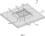
- FIG. 3 is a diagram illustrating an antenna unit 200, according to an embodiment of the present disclosure.
- the antenna unit 200 includes a first microstrip antenna 210, a second microstrip antenna 220, a first feeder line 230, and a second feeder line 240.
- the first microstrip antenna 210 includes a first radiating layer 211 and a first dielectric layer 212, which are attached, and an operating band of the first microstrip antenna 210 includes a first band.
- the second microstrip antenna 220 includes a second radiating layer 221, a second dielectric layer 222, and a ground layer 223, which are sequentially attached.
- the second radiating layer 221 is also attached to a side of the first dielectric layer 212 facing away from the first radiating layer 211, and an operating band of the second microstrip antenna 220 includes a second band which is smaller/less than the first band.
- the first radiating layer 211, the second radiating layer 221, and the ground layer 223 are all conductive metal layers, such as a copper layer, an aluminum layer and the like.
- the first dielectric layer 212 and the second dielectric layer 222 are non-conductive insulating layers, such as a rubber layer, a plastic layer, and the like. The first dielectric layer 212 and the second dielectric layer 222 support and isolate the corresponding metal layers.
- the operating frequency of the first band includes a highfrequency band of 5G communication, such as 40.5 to 43.5GHz.
- a highfrequency band of 5G communication such as 40.5 to 43.5GHz.
- it can be 40.5GHz, 41GHz, 41.5GHz, 42GHz, 42.5GHz, 43GHz, 43.5GHz, etc.
- the first microstrip antenna 210 supports frequencies in a band number n259.
- the operating frequency of the second band includes a low-frequency band of 5G communication, such as 26.5 to 29.5GHz.
- it can be 26.5GHz, 26.8GHz, 26.9GHz, 27GHz, 27.5GHz, 27.7GHz, 27.9GHz, 28GHz, 28.4GHz, 28.9GHz, 29GHz, 29.5GHz, etc.
- the second microstrip antenna 220 supports frequencies in a band number n257.
- the first feeder line 230 is electrically connected to/with the first radiating layer 211 and the second radiating layer 221.
- the second radiating layer 221 can be used as a ground layer of the first microstrip antenna 210.
- the first feeder line 230 is provided in various forms.
- the first feeder line 230 is a coaxial feeder line that intersects the layer of the first microstrip antenna 210.
- the first feeder line 230 is a coaxial feeder line that penetrates into the layer of the first microstrip antenna 210.
- the first feeder line 230 is a lead wire and can be electrically connected to the first radiating layer 211 and the second radiating layer 221 directly from the outside of the first microstrip antenna 210.
- the first feeder line 230 is a coaxial feeder line, and includes a first inner feeder line 231, a first insulated wire 233 and a first outer feeder line 232 coaxially arranged from inside to outside.
- the first feeder line 230 penetrates or intersects from the ground layer 223, and the first outer feeder line 232 and the first insulated wire 233 are cut off by the second radiating layer 221.
- the first outer feeder line 232 is electrically connected to the second radiating layer 221.
- the first inner feeder line 231 is cut off by the first dielectric layer 212, and the first inner feeder line 231 is electrically connected to the first radiating layer 211.
- an axis of the first feeder line 230 can be perpendicular to the layers of the first microstrip antenna 210 and the second microstrip antenna 220.
- the first insulated wire 233 isolates the first inner feeder line 231 form the first outer feeder line 232.
- the first feeder line 230 of the above structure regularizes the structure of the antenna unit 200, which is advantageous for reducing the volume.
- the second feeder line 240 is electrically connected to the second radiating layer 221 and the ground layer 223.
- the second feeder line 240 is provided in various forms.
- the second feeder line 240 is a coaxial feeder line that penetrates into the layer(s) of the second microstrip antenna 220.
- the second feeder line 240 is a coaxial feeder line that intersects the layer(s) of the second microstrip antenna 220.
- the second feeder line 240 is a lead wire and can be electrically connected to the second radiating layer 221 and the ground layer 223 directly from the outside of the second microstrip antenna 220.
- the second feeder line 240 is a coaxial feeder line
- the second feeder line 240 includes a second inner feeder line 241, a second insulated wire 243 and a second outer feeder line 242 coaxially arranged from inside to outside.
- the second feeder line 240 penetrates or intersects from the ground layer 223, and the second outer feeder line 242 and the second insulated wire 243 are cut off by the ground layer 223.
- the second outer feeder line 242 is electrically connected to the ground layer 223.
- the second inner feeder line 241 is cut off by the second dielectric layer 222, and the second inner feeder line 241 is electrically connected to the second radiating layer 221.
- an axis of the second feeder line 240 is perpendicular to the layers of the first microstrip antenna 210 and the second microstrip antenna 220.
- the second insulated wire 243 isolates the second inner feeder line 241 from the second outer feeder line 242.
- the second feeder line 240 of the above structure regularizes the structure of the antenna unit 200, which is advantageous for reducing the volume.
- the antenna unit 200 in the embodiments of the disclosure is based on the structure of the first microstrip antenna 210 and the second microstrip antenna 220 which are attached to each other, so that the structure of the antenna unit 200 is compact and three-dimensional, which is conducive to reducing the occupied area of the antenna unit 200.
- the first microstrip antenna 210 is fed by the first feeder line 230
- the second microstrip antenna 220 is fed by the second feeder line 240 to achieve independent tuning.
- the antenna unit 200 has good robustness to dimensional errors, has a good gain, achieves dual-frequency independent tuning in 5G communication, and can be used in highly integrated electronic devices.
- a projection area of the first radiating layer 211 on the first dielectric layer 212, a projection area of the second radiating layer 221 on the second dielectric layer 222 and a projection area of the ground layer 223 on the second dielectric layer 222 are reduced sequentially.
- the length and width of the first radiating layer are smaller than the length and width of the first dielectric area, which are smaller than the length and width of the second radiating layer.
- the length and width of the first radiating layer are smaller than the length and width of the first dielectric area, which are smaller than the length and width of the second radiating layer, which are smaller than the length and width of the ground layer.
- the increase of the ground area of the first microstrip antenna 210 and the increase of the ground area of the second microstrip antenna 220 are beneficial for the first microstrip antenna 210 and the second microstrip antenna 220 to have a good gain.
- the first feeder line 230 can also be electrically connected to the ground layer 223.
- the first outer feeder line 232 is electrically connected to the ground layer 223. In this way, the ground area of the first microstrip antenna 210 is further increased, thereby improving the gain of the first microstrip antenna 210.
- a projection area of the first radiating layer 211 on the second radiating layer 221 is centered with the middle of the second radiating layer 221.
- the center of the projection area of the first radiating layer is aligned with the center of the second radiating layer.
- the radiation patterns of the first microstrip antenna 210 and the second microstrip antenna 220 are more regular, so as to avoid a large offset therebetween.
- the radiation direction of the antenna unit 200 is regular, which is conducive to adjusting an arrangement position of the antenna unit 200 in the electronic device.
- the structures of the first radiating layer 211, the second radiating layer 221, and the ground layer 223 have an important influence on the performance of the antenna unit 200.
- the disclosure provides the following examples for the structures of the first radiating layer 211, the second radiating layer 221, and the ground layer 223.
- At least one of the projection areas of the first radiating layer 211 on the first dielectric layer 212, the projection area of the second radiating layer 221 on the second dielectric layer 222 or the projection area of the ground layer 223 on the second dielectric layer 222 is circular, square, elliptical ring-shaped, fan-shaped, semicircular, triangular or irregular.
- each film layer adopting/of the above structure is beneficial for the antenna unit 200 to have a good gain, and the structures are simple and easy to set.
- the dimensions and specifications of the first radiating layer 211, the second radiating layer 221, the ground layer 223, the first dielectric layer 212, and the second dielectric layer 222 have an important influence on the performance of the antenna unit 200.
- the disclosure provides the following examples for the structure of the antenna unit 200.
- the projection area of the first radiating layer 211 on the first dielectric layer 212 is a square with a side length of 1.5 to 2mm. For example, it can be 1.5mm, 1.6mm, 1.7mm, 1.72mm, 1.8mm, 1.9mm, 2mm, etc. And/or, the projection area of the first dielectric layer 212 on the second radiating layer 221 is a square with a side length of 2.1 to 2.5mm. For example, it can be 2.1mm, 2.2mm, 2.3mm, 2.4mm, 2.5mm, etc. And/or, the projection area of the second radiating layer 221 on the second dielectric layer 222 is a square with a side length of 2.5 to 2.8mm.
- the projection area of the ground layer 223 on the second dielectric layer 222 is a square with a side length of 4 to 5mm.
- it can be 4mm, 4.1mm, 4.2mm, 4.3mm, 4.4mm, 4.5mm, 4.6mm, 4.7mm, 4.8mm, 4.9mm, 5mm, etc.
- the first dielectric layer 212 has a thickness of 0.3 to 0.4mm.
- the antenna unit 200 has a small volume, a small thickness, a low profile, and good robustness to dimensional errors, and is beneficial to be applied to highly integrated electronic devices.
- the antenna unit 200 can achieve 5G dual-frequency bands which are independently tuned and has a good gain.
- FIG. 4 is a top view illustrating an antenna unit 200, according to an embodiment of the present disclosure.
- the projection area of the first radiating layer 211 on the first dielectric layer 212, the projection area of the second radiating layer 221 on the second dielectric layer 222, and the projection area of the ground layer 223 (not shown in FIG. 4 , refer to FIG. 2 ) on the second dielectric layer 222 are all squares, and centers of those overlap.
- the first feeder line 230 penetrates or intersects the first microstrip antenna 210 vertically, and a distance between an axis of the first feeder line 230 and the center(s) is 0.3 to 0.4mm.
- the second feeder line 240 penetrates or intersects the second microstrip antenna 220 vertically, and a distance between an axis of the second feeder line 240 and the center(s) is 0.45 to 0.55mm.
- it can be 0.45mm, 0.46mm, 0.47mm, 0.48mm, 0.49mm, 0.5mm, 0.51mm, 0.52mm, 0.53mm, 0.54mm, 0.55mm, etc.
- the positions of the first feeder line 230 and the second feeder line 240 are set so that the antenna impedances of the corresponding first microstrip antenna 210 and the second microstrip antenna 220 are close to 50 ohms, thereby making the first microstrip antenna 210 better match with the first feeder line 230 and the second microstrip antenna 220 better match with the second feeder line 240.
- the energy emitted from the first feeder line 230 can be more radiated out by the first microstrip antenna 210
- energy emitted from the second feeder line 240 can be more radiated out by the second microstrip antenna 220, which is conducive to improving a standing" wave ratio.
- the projection area of the first radiating layer 211 on the first dielectric layer 212 is a square with a side length of 1.72mm.
- the projection area of the first dielectric layer 212 on the second radiating layer 221 is a square with a side length of 2.2mm.
- the projection area of the second radiating layer 221 on the second dielectric layer 222 is a square with a side length of 2.64mm.
- the projection area of the ground layer 223 on the second dielectric layer 222 is a square with a side length of 5mm.
- the first dielectric layer 212 has a thickness of 0.335mm, and the second dielectric layer 222 has a thickness of 0.254mm.
- the projection area of the first radiating layer 211 on the first dielectric layer 212, the projection area of the second radiating layer 221 on the second dielectric layer 222, and the projection area of the ground layer 223 on the second dielectric layer 222 are all squares, and centers of those overlap.
- the first feeder line 230 penetrates or intersects the first microstrip antenna 210 vertically, and the distance between the axis of the first feeder line 230 and the center is 0.36mm.
- the second feeder line 240 penetrates or intersects the second microstrip antenna 220 vertically, and the distance between the axis of the second feeder line 240 and the center is 0.5mm.
- the antenna unit 200 has a small volume, a small thickness, a low profile, and good robustness to dimensional errors, and is beneficial to be applied to highly integrated electronic devices.
- the antenna unit 200 can achieve 5G dual-frequency bands that are independently tuned and has a good gain and a better standing wave ratio.
- the performance of the antenna unit 200 will be further described below in conjunction with a performance detection chart of the antenna unit 200.
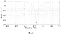
- FIG. 5 is a return loss view illustrating an antenna unit 200 at 28.4GHz, according to an embodiment of the present disclosure.
- a return loss of the antenna unit 200 in a range of about 27.8 to 29GHz is less than -10dB, which enables the antenna unit 200 to operate stably in the range of 27.8 to 29GHz and minimize the return loss at 28.4GHz.
- the antenna unit 200 has a radiation performance at 28.4GHz.
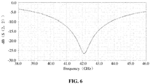
- FIG. 6 is a return loss view illustrating an antenna unit 200 at 42GHz, according to an embodiment of the present disclosure. As illustrated in FIG.
- a return loss of the antenna unit 200 in a range of about 40.6 to 43.8GHz is less than -10dB, which enables the antenna unit 200 to operate stably in the range of 40.6 to 43.8GHz and minimize the return loss at 42.1GHz.
- the antenna unit 200 has a radiation performance at 42.1GHz. With reference to FIG. 5 and FIG. 6 , it can be known that the antenna unit 200 in the disclosure can operate/work in a band range of 27.8 to 29GHz (band number n257) and of 40.6 to 43.8GHz (band number n259).
- FIG. 7 is a gain view illustrating an antenna unit 200 at 28.4GHz, according to an embodiment of the present disclosure.
- the gain of the curve A1 is greater than 0 when Theta range is between -50.0 deg and 50.0 deg
- the gain of the curve B1 is greater than 0 when Theta range is between -60.0 deg and 60.0 deg.
- FIG. 7 and FIG. 8 it can be known that the antenna unit 200 in the disclosure has a higher gain in the bands n257 and n259.
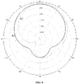
- FIG. 9 is a two-dimensional radiation pattern illustrating an antenna unit 200 at 28.4GHz, according to an embodiment of the present disclosure.
- regions occupied by the curve A3 and the curve B3 are relatively wide, which indicates that the radiation direction of the antenna unit 200 at 28.4GHz is relatively wide, and the radiation range is large.
- FIG. 10 is a two-dimensional radiation pattern illustrating an antenna unit 200 at 42GHz, according to an embodiment of the present disclosure.
- regions occupied by the curve A4 and the curve B4 are relatively wide, which indicates that the radiation direction of the antenna unit 200 at 42GHz is relatively wide, and the radiation range is large.
- FIG. 9 and FIG. 10 it can be known that the radiation direction of the antenna unit 200 at 28.4GHz and 42GHz is relatively wide and the radiation range is relatively large, which makes the radiation angle range of a 5G signal relatively large and is conducive to the application of the antenna unit 200 in 5G communication.
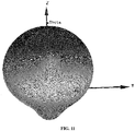
- FIG. 11 is a three-dimensional radiation pattern illustrating an antenna unit 200 at 28.4GHz, according to an embodiment of the present disclosure, in which a darker color represents higher radiation energy.
- the radiant energy of an upper hemisphere is higher than that of a lower hemisphere.
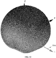
- FIG. 12 is a three-dimensional radiation pattern illustrating an antenna unit 200 at 42GHz, according to an embodiment of the present disclosure.
- the radiant energy of an upper hemisphere is higher than that of a lower hemisphere.
- the antenna unit 200 has high radiant energy in a z-axis direction and has better radiation performance.
- FIGS. 7 to 12 are analyzed.
- the antenna unit 200 in the embodiments of the disclosure can reduce the floor area, has the characteristics of small volume, small thickness, low profile, good robustness to dimensional errors, etc., and is beneficial to be applied to highly integrated electronic devices.
- the antenna unit 200 can independently tune 5G bands in two-band numbers n257 and n259 and has a good gain.
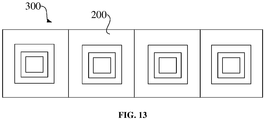
- FIG. 13 is a structural diagram illustrating an array antenna, according to an embodiment of the present disclosure.
- the array antenna 300 includes at least two antenna units 200 of any of the types mentioned above, and a distance between two adjacent antenna units 200 is 0.5 to 0.7 times the operating wavelength of the antenna unit 200.
- dual-frequency independent tuning is achieved in 5G communication, and the radiant energy of the antenna units 200 is concentrated, so that the array antenna 300 has a higher gain.
- the array antenna 300 includes four antenna units 200 arranged side by side.
- the electronic device in an embodiment of the disclosure is based on a compact and three-dimensional structure of the antenna unit 200 and the array antenna 300, which is conducive to achieving high integration and volume miniaturization of the electronic device. Moreover, the electronic device can easily achieve dual-frequency independent tuning in 5G communication, has a good 5G radiation performance, and is conducive to improving user experience.
- the relevant part can refer to the partial description of the embodiments of the antenna unit.
- the embodiments of the array antenna and the electronic device are complementary to the embodiments of the antenna unit.
Landscapes
- Physics & Mathematics (AREA)
- Electromagnetism (AREA)
- Engineering & Computer Science (AREA)
- Computer Networks & Wireless Communication (AREA)
- Details Of Aerials (AREA)
- Waveguide Aerials (AREA)
Abstract
Description
- The disclosure relates to the field of 5G communications, and more particularly, to an antenna unit, an array antenna, and an electronic device.
- With the research of a 5G technology (5th generation mobile networks), antenna units of more and more electronic devices support 5G communication(s). However, due to user requirements such as portability and the like, the size of the electronic device is limited, which is not conducive to arranging a plurality of antenna units supporting different bands, and thus is not conducive to the electronic device supporting a plurality of bands for/in 5G communication.
- According to a first aspect of the disclosure, there is provided an antenna unit. The antenna unit includes: a first microstrip antenna, comprising a first radiating layer coupled to a first dielectric layer wherein the first microstrip antenna operates at a first band, a second microstrip antenna, comprising a second radiating layer, a second dielectric layer, and a ground layer, sequentially coupled, wherein the second radiating layer is coupled to a side of the first dielectric layer facing away from the first radiating layer, and wherein the second microstrip antenna operates at a second band that is smaller than the first band, a first feeder line, electrically coupled to the first radiating layer and the second radiating layer, and a second feeder line, electrically coupled to the second radiating layer and the ground layer.
- According to a second aspect of the disclosure, there is provided an array antenna. The array antenna includes at least two antenna units, at least one of the two antenna units comprising: a first microstrip antenna, comprising a first radiating layer coupled to a first dielectric layer wherein the first microstrip antenna operates at a first band, a second microstrip antenna, comprising a second radiating layer, a second dielectric layer, and a ground layer, sequentially coupled, wherein the second radiating layer is coupled to a side of the first dielectric layer facing away from the first radiating layer, and wherein the second microstrip antenna operates at a second band that is smaller than the first band, a first feeder line, electrically coupled to the first radiating layer and the second radiating layer, and a second feeder line, electrically coupled to the second radiating layer and the ground layer, wherein a distance between centers of two adjacent antenna units is 0.5 to 0.7 times an operating wavelength of the antenna unit.
- According to a third aspect of the disclosure, there is provided an electronic device. The electronic device includes at least one antenna unit or comprising an array antenna including at least two antenna units. The antenna units comprising: a first microstrip antenna, comprising a first radiating layer coupled to a first dielectric layer wherein the first microstrip antenna operates at a first band, a second microstrip antenna, comprising a second radiating layer, a second dielectric layer, and a ground layer, sequentially coupled, wherein the second radiating layer is coupled to a side of the first dielectric layer facing away from the first radiating layer, and wherein the second microstrip antenna operates at a second band that is smaller than the first band, a first feeder line, electrically coupled to the first radiating layer and the second radiating layer, and a second feeder line, electrically coupled to the second radiating layer and the ground layer, wherein a distance between centers of two adjacent antenna units of the array antenna is 0.5 to 0.7 times an operating wavelength of the antenna unit.
- It is to be understood that both the foregoing general description and the following detailed description are examples and explanatory only and are not restrictive of the present disclosure, as claimed.
-
-
FIG. 1 is a partial structural diagram illustrating an electronic device, according to an example of the present disclosure. -
FIG. 2 is a partial cross-sectional view illustrating an antenna unit, according to an example of the present disclosure. -
FIG. 3 is a diagram illustrating an antenna unit, according to an example of the present disclosure. -
FIG. 4 is a top view illustrating an antenna unit, according to an example of the present disclosure. -
FIG. 5 is a return loss view illustrating an antenna unit at 28.4GHz, according to an example of the present disclosure. -
FIG. 6 is a return loss view illustrating an antenna unit at 42GHz, according to an example of the present disclosure. -
FIG. 7 is a gain view illustrating an antenna unit at 28.4GHz, according to an example of the present disclosure. -
FIG. 8 is a gain view illustrating an antenna unit at 42GHz, according to an example of the present disclosure. -
FIG. 9 is a two-dimensional radiation pattern illustrating an antenna unit at 28.4GHz, according to an example of the present disclosure. -
FIG. 10 is a two-dimensional radiation pattern illustrating an antenna unit at 42GHz, according to an example of the present disclosure. -
FIG. 11 is a three-dimensional radiation pattern illustrating an antenna unit at 28.4GHz, according to an example of the present disclosure. -
FIG. 12 is a three-dimensional radiation pattern illustrating an antenna unit at 42GHz, according to an example of the present disclosure. -
FIG. 13 is a structural diagram illustrating an array antenna, according to an example of the present disclosure. - Reference will now be made in detail to embodiments, examples of which are illustrated in the accompanying drawings. The following description refers to the accompanying drawings in which the same numbers in different drawings represent the same or similar elements unless otherwise represented. The implementations set forth in the following description of embodiments do not represent all implementations consistent with the disclosure. Instead, they are merely examples of apparatuses and methods consistent with aspects related to the disclosure as recited in the appended claims.
- The terms used in the disclosure are for the purpose of describing particular embodiments only, and are not intended to limit the disclosure. Unless otherwise defined, technical terms or scientific terms used in the disclosure should be understood in the ordinary meaning of those of ordinary skill in the art to which the disclosure pertains. The words "first," "second," and similar terms used in the specification and claims of the disclosure are not intended to indicate any order, quantity or importance, but only to distinguish different components. Similarly, similar words "a" or "an" and the like do not denote a quantity limitation but mean that there is at least one. Unless otherwise specified, similar words "comprise" or "include" and the like mean that elements or objects preceding "comprise" or "include" encompass listed elements or objects following "comprise" or "include" and their equivalents, and do not exclude other elements or objects. Similar words "connect" or "connected" and the like are not limited to physical or mechanical connections, and can include electrical connections, whether direct or indirect.
- "A/an," "the," and "this" in a singular form in the specification of the disclosure and the appended claims are also intended to include a plural form unless other meanings are clearly denoted throughout the disclosure. It is also to be understood that the term "and/or" used in the disclosure refers to and includes one or any or all possible combinations of multiple associated items that are listed.
- In some embodiments, due to user requirements such as portability and the like, the integration degree of an electronic device is high, and the dimension and specification of the electronic device are limited, which is not conducive to arranging a plurality of antenna units that support different bands in the electronic device, and is not conducive to the electronic device supporting multi-band 5G communication. Moreover, the plurality of antenna units cannot be independently tuned, and it is difficult to tune. The resonance of different bands is badly robust to the size of the antenna units, which is not conducive to the electronic device supporting a multi-band 5G communication function.
- An antenna unit can be one or more antennas arranged to transmit in at least one or more frequency bands. See
FIGS. 2 ,3 , and4 for an example structure of an antenna unit. For example, an antenna unit can have two antennas arranged to transmit in two frequency bands, one for each. - Embodiments of the disclosure provide an antenna unit, an array antenna, and an electronic device. The details are as follows.
-
FIG. 1 is a partial structural diagram illustrating an electronic device, according to an embodiment of the present disclosure. As illustrated inFIG. 1 , the electronic device includes abody 100 and anantenna unit 200 or anarray antenna 300 in the disclosure. Theantenna unit 200 or thearray antenna 300 is disposed in thebody 100 to support a Wifi (a wireless local area network technology based on an IEEE 802.11 standard) function, a Global Positioning System (GPS) function, and other antenna communication functions of the electronic device. - The electronic device in the embodiments of the disclosure includes, but is not limited to, mobile phones, tablet computers, iPads, digital broadcasting terminals, messaging devices, game consoles, medical devices, fitness devices, personal digital assistants, smart wearable devices, smart TVs, etc.
-
FIG. 2 is a partial cross-sectional view illustrating anantenna unit 200, according to an embodiment of the present disclosure.FIG. 3 is a diagram illustrating anantenna unit 200, according to an embodiment of the present disclosure. With reference toFIG. 2 andFIG. 3 , theantenna unit 200 includes afirst microstrip antenna 210, asecond microstrip antenna 220, afirst feeder line 230, and asecond feeder line 240. Thefirst microstrip antenna 210 includes a first radiatinglayer 211 and a firstdielectric layer 212, which are attached, and an operating band of thefirst microstrip antenna 210 includes a first band. Thesecond microstrip antenna 220 includes a second radiatinglayer 221, a seconddielectric layer 222, and aground layer 223, which are sequentially attached. The second radiatinglayer 221 is also attached to a side of the firstdielectric layer 212 facing away from the firstradiating layer 211, and an operating band of thesecond microstrip antenna 220 includes a second band which is smaller/less than the first band. - In some embodiments of the disclosure, the first
radiating layer 211, the secondradiating layer 221, and theground layer 223 are all conductive metal layers, such as a copper layer, an aluminum layer and the like. The firstdielectric layer 212 and the seconddielectric layer 222 are non-conductive insulating layers, such as a rubber layer, a plastic layer, and the like. The firstdielectric layer 212 and the seconddielectric layer 222 support and isolate the corresponding metal layers. - In some embodiments, the operating frequency of the first band includes a highfrequency band of 5G communication, such as 40.5 to 43.5GHz. For example, it can be 40.5GHz, 41GHz, 41.5GHz, 42GHz, 42.5GHz, 43GHz, 43.5GHz, etc. That is, the
first microstrip antenna 210 supports frequencies in a band number n259. The operating frequency of the second band includes a low-frequency band of 5G communication, such as 26.5 to 29.5GHz. For example, it can be 26.5GHz, 26.8GHz, 26.9GHz, 27GHz, 27.5GHz, 27.7GHz, 27.9GHz, 28GHz, 28.4GHz, 28.9GHz, 29GHz, 29.5GHz, etc. That is, thesecond microstrip antenna 220 supports frequencies in a band number n257. - The
first feeder line 230 is electrically connected to/with thefirst radiating layer 211 and thesecond radiating layer 221. Thesecond radiating layer 221 can be used as a ground layer of thefirst microstrip antenna 210. Thefirst feeder line 230 is provided in various forms. For example, thefirst feeder line 230 is a coaxial feeder line that intersects the layer of thefirst microstrip antenna 210. In another example, thefirst feeder line 230 is a coaxial feeder line that penetrates into the layer of thefirst microstrip antenna 210. For example, thefirst feeder line 230 is a lead wire and can be electrically connected to thefirst radiating layer 211 and thesecond radiating layer 221 directly from the outside of thefirst microstrip antenna 210. - In some embodiments, the
first feeder line 230 is a coaxial feeder line, and includes a firstinner feeder line 231, a firstinsulated wire 233 and a firstouter feeder line 232 coaxially arranged from inside to outside. Thefirst feeder line 230 penetrates or intersects from theground layer 223, and the firstouter feeder line 232 and the firstinsulated wire 233 are cut off by thesecond radiating layer 221. The firstouter feeder line 232 is electrically connected to thesecond radiating layer 221. The firstinner feeder line 231 is cut off by thefirst dielectric layer 212, and the firstinner feeder line 231 is electrically connected to thefirst radiating layer 211. It is to be noted that an axis of thefirst feeder line 230 can be perpendicular to the layers of thefirst microstrip antenna 210 and thesecond microstrip antenna 220. The firstinsulated wire 233 isolates the firstinner feeder line 231 form the firstouter feeder line 232. Thefirst feeder line 230 of the above structure regularizes the structure of theantenna unit 200, which is advantageous for reducing the volume. - With continued reference to
FIG. 2 , thesecond feeder line 240 is electrically connected to thesecond radiating layer 221 and theground layer 223. Thesecond feeder line 240 is provided in various forms. For example, thesecond feeder line 240 is a coaxial feeder line that penetrates into the layer(s) of thesecond microstrip antenna 220. In another example, thesecond feeder line 240 is a coaxial feeder line that intersects the layer(s) of thesecond microstrip antenna 220. For example, thesecond feeder line 240 is a lead wire and can be electrically connected to thesecond radiating layer 221 and theground layer 223 directly from the outside of thesecond microstrip antenna 220. - In some embodiments, the
second feeder line 240 is a coaxial feeder line, and thesecond feeder line 240 includes a secondinner feeder line 241, a secondinsulated wire 243 and a secondouter feeder line 242 coaxially arranged from inside to outside. Thesecond feeder line 240 penetrates or intersects from theground layer 223, and the secondouter feeder line 242 and the secondinsulated wire 243 are cut off by theground layer 223. The secondouter feeder line 242 is electrically connected to theground layer 223. The secondinner feeder line 241 is cut off by thesecond dielectric layer 222, and the secondinner feeder line 241 is electrically connected to thesecond radiating layer 221. It is to be noted that an axis of thesecond feeder line 240 is perpendicular to the layers of thefirst microstrip antenna 210 and thesecond microstrip antenna 220. The secondinsulated wire 243 isolates the secondinner feeder line 241 from the secondouter feeder line 242. Thesecond feeder line 240 of the above structure regularizes the structure of theantenna unit 200, which is advantageous for reducing the volume. - The
antenna unit 200 in the embodiments of the disclosure is based on the structure of thefirst microstrip antenna 210 and thesecond microstrip antenna 220 which are attached to each other, so that the structure of theantenna unit 200 is compact and three-dimensional, which is conducive to reducing the occupied area of theantenna unit 200. Thefirst microstrip antenna 210 is fed by thefirst feeder line 230, and thesecond microstrip antenna 220 is fed by thesecond feeder line 240 to achieve independent tuning. Based on the above, theantenna unit 200 has good robustness to dimensional errors, has a good gain, achieves dual-frequency independent tuning in 5G communication, and can be used in highly integrated electronic devices. - As the gain of the
antenna unit 200 is higher, the distance of radio wave transmission is longer, and the 5G communication performance is better. In order to make theantenna unit 200 have a good gain, in some embodiments, with continued reference toFIG. 2 , a projection area of thefirst radiating layer 211 on thefirst dielectric layer 212, a projection area of thesecond radiating layer 221 on thesecond dielectric layer 222 and a projection area of theground layer 223 on thesecond dielectric layer 222 are reduced sequentially. For example, the length and width of the first radiating layer are smaller than the length and width of the first dielectric area, which are smaller than the length and width of the second radiating layer. In another example, the length and width of the first radiating layer are smaller than the length and width of the first dielectric area, which are smaller than the length and width of the second radiating layer, which are smaller than the length and width of the ground layer. In some embodiments, in this way, it is beneficial for thefirst microstrip antenna 210 to support a first band of 5G communication and for thesecond microstrip antenna 220 to support a second band of 5G communication. Moreover, the increase of the ground area of thefirst microstrip antenna 210 and the increase of the ground area of thesecond microstrip antenna 220 are beneficial for thefirst microstrip antenna 210 and thesecond microstrip antenna 220 to have a good gain. - Furthermore, with continued reference to
FIG. 2 , thefirst feeder line 230 can also be electrically connected to theground layer 223. In the case that thefirst feeder line 230 is a coaxial feeder line, the firstouter feeder line 232 is electrically connected to theground layer 223. In this way, the ground area of thefirst microstrip antenna 210 is further increased, thereby improving the gain of thefirst microstrip antenna 210. - In some embodiments, a projection area of the
first radiating layer 211 on thesecond radiating layer 221 is centered with the middle of thesecond radiating layer 221. For example, the center of the projection area of the first radiating layer is aligned with the center of the second radiating layer. In some embodiments, in this way, in a three-dimensional space, the radiation patterns of thefirst microstrip antenna 210 and thesecond microstrip antenna 220 are more regular, so as to avoid a large offset therebetween. Thus, the radiation direction of theantenna unit 200 is regular, which is conducive to adjusting an arrangement position of theantenna unit 200 in the electronic device. - The structures of the
first radiating layer 211, thesecond radiating layer 221, and theground layer 223 have an important influence on the performance of theantenna unit 200. The disclosure provides the following examples for the structures of thefirst radiating layer 211, thesecond radiating layer 221, and theground layer 223. - At least one of the projection areas of the
first radiating layer 211 on thefirst dielectric layer 212, the projection area of thesecond radiating layer 221 on thesecond dielectric layer 222 or the projection area of theground layer 223 on thesecond dielectric layer 222 is circular, square, elliptical ring-shaped, fan-shaped, semicircular, triangular or irregular. In some embodiments, each film layer adopting/of the above structure is beneficial for theantenna unit 200 to have a good gain, and the structures are simple and easy to set. - The dimensions and specifications of the
first radiating layer 211, thesecond radiating layer 221, theground layer 223, thefirst dielectric layer 212, and thesecond dielectric layer 222 have an important influence on the performance of theantenna unit 200. The disclosure provides the following examples for the structure of theantenna unit 200. - The projection area of the
first radiating layer 211 on thefirst dielectric layer 212 is a square with a side length of 1.5 to 2mm. For example, it can be 1.5mm, 1.6mm, 1.7mm, 1.72mm, 1.8mm, 1.9mm, 2mm, etc. And/or, the projection area of thefirst dielectric layer 212 on thesecond radiating layer 221 is a square with a side length of 2.1 to 2.5mm. For example, it can be 2.1mm, 2.2mm, 2.3mm, 2.4mm, 2.5mm, etc. And/or, the projection area of thesecond radiating layer 221 on thesecond dielectric layer 222 is a square with a side length of 2.5 to 2.8mm. For example, it can be 2.5mm, 2.6mm, 2.64mm, 2.7mm, 2.8mm, etc. And/or, the projection area of theground layer 223 on thesecond dielectric layer 222 is a square with a side length of 4 to 5mm. For example, it can be 4mm, 4.1mm, 4.2mm, 4.3mm, 4.4mm, 4.5mm, 4.6mm, 4.7mm, 4.8mm, 4.9mm, 5mm, etc. And/or, thefirst dielectric layer 212 has a thickness of 0.3 to 0.4mm. For example, it can be 0.3mm, 0.31mm, 0.32mm, 0.33mm, 0.335mm, 0.34mm, 0.35mm, 0.36mm, 0.37mm, 0.38mm, 0.39mm, 0.4mm, etc. And/or, thesecond dielectric layer 222 has a thickness of 0.2 to 0.3mm. For example, it can be 0.2mm, 0.21mm, 0.22mm, 0.23mm, 0.24mm, 0.25mm, 0.254mm, 0.26mm, 0.27mm, 0.28mm, 0.29mm, 0.3mm, etc. In some embodiments, by using such an arrangement, theantenna unit 200 has a small volume, a small thickness, a low profile, and good robustness to dimensional errors, and is beneficial to be applied to highly integrated electronic devices. In addition, theantenna unit 200 can achieve 5G dual-frequency bands which are independently tuned and has a good gain. -
FIG. 4 is a top view illustrating anantenna unit 200, according to an embodiment of the present disclosure. As illustrated inFIG. 4 , the projection area of thefirst radiating layer 211 on thefirst dielectric layer 212, the projection area of thesecond radiating layer 221 on thesecond dielectric layer 222, and the projection area of the ground layer 223 (not shown inFIG. 4 , refer toFIG. 2 ) on thesecond dielectric layer 222 are all squares, and centers of those overlap. Thefirst feeder line 230 penetrates or intersects thefirst microstrip antenna 210 vertically, and a distance between an axis of thefirst feeder line 230 and the center(s) is 0.3 to 0.4mm. For example, it can be 0.3mm, 0.31mm, 0.32mm, 0.33mm, 0.34mm, 0.35mm, 0.36mm, 0.37mm, 0.38mm, 0.39mm, 0.4mm, etc. And/or, thesecond feeder line 240 penetrates or intersects thesecond microstrip antenna 220 vertically, and a distance between an axis of thesecond feeder line 240 and the center(s) is 0.45 to 0.55mm. For example, it can be 0.45mm, 0.46mm, 0.47mm, 0.48mm, 0.49mm, 0.5mm, 0.51mm, 0.52mm, 0.53mm, 0.54mm, 0.55mm, etc. In some embodiments, the positions of thefirst feeder line 230 and thesecond feeder line 240 are set so that the antenna impedances of the correspondingfirst microstrip antenna 210 and thesecond microstrip antenna 220 are close to 50 ohms, thereby making thefirst microstrip antenna 210 better match with thefirst feeder line 230 and thesecond microstrip antenna 220 better match with thesecond feeder line 240. Moreover, the energy emitted from thefirst feeder line 230 can be more radiated out by thefirst microstrip antenna 210, and energy emitted from thesecond feeder line 240 can be more radiated out by thesecond microstrip antenna 220, which is conducive to improving a standing" wave ratio. - In particular, the projection area of the
first radiating layer 211 on thefirst dielectric layer 212 is a square with a side length of 1.72mm. The projection area of thefirst dielectric layer 212 on thesecond radiating layer 221 is a square with a side length of 2.2mm. The projection area of thesecond radiating layer 221 on thesecond dielectric layer 222 is a square with a side length of 2.64mm. The projection area of theground layer 223 on thesecond dielectric layer 222 is a square with a side length of 5mm. Thefirst dielectric layer 212 has a thickness of 0.335mm, and thesecond dielectric layer 222 has a thickness of 0.254mm. The projection area of thefirst radiating layer 211 on thefirst dielectric layer 212, the projection area of thesecond radiating layer 221 on thesecond dielectric layer 222, and the projection area of theground layer 223 on thesecond dielectric layer 222 are all squares, and centers of those overlap. Thefirst feeder line 230 penetrates or intersects thefirst microstrip antenna 210 vertically, and the distance between the axis of thefirst feeder line 230 and the center is 0.36mm. Thesecond feeder line 240 penetrates or intersects thesecond microstrip antenna 220 vertically, and the distance between the axis of thesecond feeder line 240 and the center is 0.5mm. By such an arrangement, theantenna unit 200 has a small volume, a small thickness, a low profile, and good robustness to dimensional errors, and is beneficial to be applied to highly integrated electronic devices. In addition, theantenna unit 200 can achieve 5G dual-frequency bands that are independently tuned and has a good gain and a better standing wave ratio. - The performance of the
antenna unit 200 will be further described below in conjunction with a performance detection chart of theantenna unit 200. -
FIG. 5 is a return loss view illustrating anantenna unit 200 at 28.4GHz, according to an embodiment of the present disclosure. As illustrated inFIG. 5 , a return loss of theantenna unit 200 in a range of about 27.8 to 29GHz is less than -10dB, which enables theantenna unit 200 to operate stably in the range of 27.8 to 29GHz and minimize the return loss at 28.4GHz. Theantenna unit 200 has a radiation performance at 28.4GHz.FIG. 6 is a return loss view illustrating anantenna unit 200 at 42GHz, according to an embodiment of the present disclosure. As illustrated inFIG. 6 , a return loss of theantenna unit 200 in a range of about 40.6 to 43.8GHz is less than -10dB, which enables theantenna unit 200 to operate stably in the range of 40.6 to 43.8GHz and minimize the return loss at 42.1GHz. Theantenna unit 200 has a radiation performance at 42.1GHz. With reference toFIG. 5 andFIG. 6 , it can be known that theantenna unit 200 in the disclosure can operate/work in a band range of 27.8 to 29GHz (band number n257) and of 40.6 to 43.8GHz (band number n259). -
FIG. 7 is a gain view illustrating anantenna unit 200 at 28.4GHz, according to an embodiment of the present disclosure. A curve A1 is a gain curve measured at a frequency of 28.4GHz and Phi = 0 degrees (deg), and a curve B1 is a gain curve measured at a frequency of 28.4GHz and Phi = 90 deg. As illustrated inFIG. 7 , the gains of the curve A1 and the curve B1 are greatest when Theta = 0.0 deg, the gain of the curve A1 is greater than 0 when Theta range is between -50.0 deg and 50.0 deg, and the gain of the curve B1 is greater than 0 when Theta range is between -60.0 deg and 60.0 deg.FIG. 8 is a gain view illustrating anantenna unit 200 at 42GHz, according to an embodiment of the present disclosure. A curve A2 is a gain curve measured at a frequency of 42GHz and Phi = 0 deg, and a curve B2 is a gain curve measured at a frequency of 42GHz and Phi = 90 deg. As illustrated inFIG. 8 , the gain of the curve A2 is greatest when Theta = 0.0 deg, and the gain of the curve A2 is greater than 0 when Theta range is between -60 deg and 55 deg. The gain of the curve B2 is greatest when Theta = 20 deg, and the gain of the curve B2 is greater than 0 when Theta range is between -30 deg and 75 deg. With reference toFIG. 7 andFIG. 8 , it can be known that theantenna unit 200 in the disclosure has a higher gain in the bands n257 and n259. -
FIG. 9 is a two-dimensional radiation pattern illustrating anantenna unit 200 at 28.4GHz, according to an embodiment of the present disclosure. A curve A3 is a two-dimensional radiation pattern measured at a frequency of 28.4GHz and Phi = 0 deg, and a curve B3 is a two-dimensional radiation pattern measured at a frequency of 28.4GHz and Phi = 90 deg. As illustrated inFIG. 9 , regions occupied by the curve A3 and the curve B3 are relatively wide, which indicates that the radiation direction of theantenna unit 200 at 28.4GHz is relatively wide, and the radiation range is large.FIG. 10 is a two-dimensional radiation pattern illustrating anantenna unit 200 at 42GHz, according to an embodiment of the present disclosure. A curve A4 is a two-dimensional radiation pattern measured at a frequency of 42GHz and Phi = 0 deg, and a curve B4 is a two-dimensional radiation pattern measured at a frequency of 42GHz and Phi = 90 deg. As illustrated inFIG. 10 , regions occupied by the curve A4 and the curve B4 are relatively wide, which indicates that the radiation direction of theantenna unit 200 at 42GHz is relatively wide, and the radiation range is large. With reference toFIG. 9 andFIG. 10 , it can be known that the radiation direction of theantenna unit 200 at 28.4GHz and 42GHz is relatively wide and the radiation range is relatively large, which makes the radiation angle range of a 5G signal relatively large and is conducive to the application of theantenna unit 200 in 5G communication. -
FIG. 11 is a three-dimensional radiation pattern illustrating anantenna unit 200 at 28.4GHz, according to an embodiment of the present disclosure, in which a darker color represents higher radiation energy. InFIG. 11 , the radiant energy of an upper hemisphere is higher than that of a lower hemisphere.FIG. 12 is a three-dimensional radiation pattern illustrating anantenna unit 200 at 42GHz, according to an embodiment of the present disclosure. InFIG. 12 , the radiant energy of an upper hemisphere is higher than that of a lower hemisphere. With reference toFIG. 11 andFIG. 12 , it can be known that theantenna unit 200 has high radiant energy in a z-axis direction and has better radiation performance. - It is to be noted that a plane where the
ground layer 223 of thesecond microstrip antenna 220 is located in an XY plane, and an axis that is perpendicular to the XY plane and passes through the center of thesecond microstrip antenna 220 is the Z-axis. Based on this orientation,FIGS. 7 to 12 are analyzed. - In summary, the
antenna unit 200 in the embodiments of the disclosure can reduce the floor area, has the characteristics of small volume, small thickness, low profile, good robustness to dimensional errors, etc., and is beneficial to be applied to highly integrated electronic devices. Theantenna unit 200 can independently tune 5G bands in two-band numbers n257 and n259 and has a good gain. -
FIG. 13 is a structural diagram illustrating an array antenna, according to an embodiment of the present disclosure. As illustrated inFIG. 13 , thearray antenna 300 includes at least twoantenna units 200 of any of the types mentioned above, and a distance between twoadjacent antenna units 200 is 0.5 to 0.7 times the operating wavelength of theantenna unit 200. In some embodiments, dual-frequency independent tuning is achieved in 5G communication, and the radiant energy of theantenna units 200 is concentrated, so that thearray antenna 300 has a higher gain. - In some embodiments, with continued reference to
FIG. 13 , thearray antenna 300 includes fourantenna units 200 arranged side by side. - The electronic device in an embodiment of the disclosure is based on a compact and three-dimensional structure of the
antenna unit 200 and thearray antenna 300, which is conducive to achieving high integration and volume miniaturization of the electronic device. Moreover, the electronic device can easily achieve dual-frequency independent tuning in 5G communication, has a good 5G radiation performance, and is conducive to improving user experience. - Since the embodiments of the array antenna and the electronic device basically correspond to the embodiments of the antenna unit, the relevant part can refer to the partial description of the embodiments of the antenna unit. The embodiments of the array antenna and the electronic device are complementary to the embodiments of the antenna unit.
- The above embodiments of the disclosure can complement each other without causing conflicts.
- The above descriptions are only examples of the present disclosure and are not intended to limit the disclosure. Any modifications, equivalent replacements, improvements, and the like made within the spirit and principle of the disclosure should fall within the scope of protection of the disclosure.
Claims (15)
- An antenna unit (200), characterized in that the antenna unit (200) comprises:a first microstrip antenna (210), comprising a first radiating layer (211) coupled to a first dielectric layer (212) wherein the first microstrip antenna (210) operates at a first band;a second microstrip antenna (220), comprising a second radiating layer (221), a second dielectric layer (222), and a ground layer (223), sequentially coupled, wherein the second radiating layer (221) is coupled to a side of the first dielectric layer (212) facing away from the first radiating layer (211), and wherein the second microstrip antenna (220) operates at a second band that is smaller than the first band;a first feeder line (230), electrically coupled to the first radiating layer (211) and the second radiating layer (221); anda second feeder line (240), electrically coupled to the second radiating layer (221) and the ground layer (223).
- The antenna unit (200) of claim 1, wherein the first radiating layer (211) is a first projection area on the first dielectric layer (212), wherein the second radiating layer (221) is a second projection area on the second dielectric layer (222), wherein the ground layer (223) is a third projection area on the second dielectric layer (222), wherein at least two of the projection areas are reduced sequentially.
- The antenna unit (200) of claim 2, wherein the first feeder line (230) is also electrically coupled to the ground layer (223).
- The antenna unit (200) of claim 2, wherein a center of the first projection area is aligned with a center of the second projection area.
- The antenna unit (200) of claim 1, further comprising at least one of:the first radiating layer (211) is a first projection area on the first dielectric layer (212) that is a square with a side length of 1.5 to 2mm;the second radiating layer (221) is a second projection area on the second dielectric layer (222) that is a square with a side length of 2.5 to 2.8mm;the ground layer (223) is a third projection area on the second dielectric layer (222) that is a square with a side length of 4 to 5mm; orthe first dielectric layer (212) is a fourth projection area on the second radiating layer (221) that is a square with a side length of 2.1 to 2.5mm..
- The antenna unit (200) of claim 1, wherein either the first dielectric layer (212) has a thickness of 0.3 to 0.4mm; or,
the second dielectric layer (222) has a thickness of 0.2 to 0.3mm; or,
the first dielectric layer (212) has a thickness of 0.3 to 0.4mm and the second dielectric layer (222) has a thickness of 0.2 to 0.3mm. - The antenna unit (200) of claim 1, wherein the first radiating layer (211) is a first projection area on the first dielectric layer (212), the second radiating layer (221) is a second projection area on the second dielectric layer (222), and the ground layer (223) is a third projection area on the second dielectric layer (222), wherein the first, second, and third projection areas are squared and the center of the projection areas overlap;
wherein the first feeder line (230) intersects the first microstrip antenna (210) and a distance between an axis of the first feeder line (230) and the center of the projection areas is 0.3 to 0.4mm; wherein the second feeder line (240) intersects the second microstrip antenna (220), and a distance between an axis of the second feeder line (240) and the center of the projection areas is 0.45 to 0.55mm. - The antenna unit (200) of claim 1, wherein the first feeder line (230) comprises:a first inner feeder line (231);a first insulated wire (233); anda first outer feeder line (232) is coaxially arranged from inside to outside, the first feeder line (230) intersects from the ground layer (223), the first outer feeder line (232) and the first insulated wire (233) are cut off by the second radiating layer (221), the first outer feeder line (232) is electrically coupled to the second radiating layer (221), the first inner feeder line (231) is cut off by the first dielectric layer (212), and the first inner feeder line (231) is electrically coupled to the first radiating layer (211).
- The antenna unit (200) of claim 1, wherein the second feeder line (240) comprises:a second inner feeder line (241);a second insulated wire (243); anda second outer feeder line (242) coaxially arranged from inside to outside, wherein the second feeder line (240) intersects from the ground layer (223), the second outer feeder line (242) and the second insulated wire (243) are cut off by the ground layer (223), the second outer feeder line (242) is electrically coupled to the ground layer (223), the second inner feeder line (241) is cut off by the second dielectric layer (222), and the second inner feeder line (241) is electrically coupled to the second radiating layer (221).
- The antenna unit (200) of any one of claims 1 to 9, wherein an operating frequency of the first band comprises 40.5 to 43.5GHz; and
an operating frequency of the second band comprises 26.5 to 29.5GHz. - An array antenna (300), characterized in that the array antenna (300) comprises at least two antenna units (200), at least one of the two antenna units (200) comprising:a first microstrip antenna (210), comprising a first radiating layer (211) coupled to a first dielectric layer (212) wherein the first microstrip antenna (210) operates at a first band;a second microstrip antenna (220), comprising a second radiating layer (221), a second dielectric layer (222) and a ground layer (223), sequentially coupled, wherein the second radiating layer (221) is coupled to a side of the first dielectric layer (212) facing away from the first radiating layer (211), and wherein the second microstrip antenna (220) operates at a second band that is smaller than the first band;a first feeder line (230), electrically coupled to the first radiating layer (211) and the second radiating layer (221); anda second feeder line (240), electrically coupled to the second radiating layer (221) and the ground layer (223);wherein a distance between centers of two adjacent antenna units (200) is 0.5 to 0.7 times an operating wavelength of the antenna unit (200).
- The array antenna (300) of claim 11, wherein the first radiating layer (211) is a first projection area on the first dielectric layer (212), wherein the second radiating layer (221) is a second projection area on the second dielectric layer (222), wherein the ground layer (223) is a third projection area on the second dielectric layer (222), wherein at least two of the projection areas are reduced sequentially.
- The array antenna (300) of claim 11, further comprising at least one of:the first radiating layer (211) is a first projection area on the first dielectric layer (212) that is a square with a side length of 1.5 to 2mm;the second radiating layer (221) is a second projection area on the second dielectric layer (222) that is a square with a side length of 2.5 to 2.8mm;the ground layer (223) is a third projection area on the second dielectric layer (222) that is a square with a side length of 4 to 5mm; orthe first dielectric layer (212) is a fourth projection area on the second radiating layer (221) that is a square with a side length of 2.1 to 2.5mm.
- The array antenna (300) of claim 11, wherein either:the first dielectric layer (212) has a thickness of 0.3 to 0.4mm;the second dielectric layer (222) has a thickness of 0.2 to 0.3mm; orthe first dielectric layer (212) has a thickness of 0.3 to 0.4mm and the second dielectric layer (222) has a thickness of 0.2 to 0.3mm.
- An electronic device, characterized in that the electronic device comprises at least one antenna unit (200) of any one of claims 1 to 10, or comprising an array antenna (300) of any one of claims 11 to 14.
Applications Claiming Priority (1)
| Application Number | Priority Date | Filing Date | Title |
|---|---|---|---|
| CN201911040141.5A CN112751178A (en) | 2019-10-29 | 2019-10-29 | Antenna unit, array antenna and electronic equipment |
Publications (1)
| Publication Number | Publication Date |
|---|---|
| EP3817145A1 true EP3817145A1 (en) | 2021-05-05 |
Family
ID=69742678
Family Applications (1)
| Application Number | Title | Priority Date | Filing Date |
|---|---|---|---|
| EP20159664.0A Pending EP3817145A1 (en) | 2019-10-29 | 2020-02-27 | Antenna unit, array antenna, and electronic device |
Country Status (3)
| Country | Link |
|---|---|
| US (1) | US11258177B2 (en) |
| EP (1) | EP3817145A1 (en) |
| CN (1) | CN112751178A (en) |
Cited By (1)
| Publication number | Priority date | Publication date | Assignee | Title |
|---|---|---|---|---|
| US20220131256A1 (en) * | 2020-10-23 | 2022-04-28 | Dongwoo Fine-Chem Co., Ltd. | Antenna device and image display device including the same |
Families Citing this family (10)
| Publication number | Priority date | Publication date | Assignee | Title |
|---|---|---|---|---|
| CN113381167B (en) * | 2020-02-25 | 2022-11-01 | 荣耀终端有限公司 | Antenna connecting device, antenna assembly and electronic equipment |
| CN113675592B (en) * | 2020-05-13 | 2023-08-04 | 北京小米移动软件有限公司 | Antenna module and terminal equipment |
| CN113708055B (en) * | 2020-05-21 | 2022-12-06 | 华为技术有限公司 | Multi-frequency dual-polarized antenna and electronic equipment |
| EP4016735A1 (en) * | 2020-12-17 | 2022-06-22 | INTEL Corporation | A multiband patch antenna |
| WO2022185855A1 (en) * | 2021-03-05 | 2022-09-09 | 株式会社村田製作所 | Antenna device and antenna unit |
| CN113764888B (en) * | 2021-08-09 | 2022-07-29 | 荣耀终端有限公司 | Antenna combination system and terminal equipment |
| CN113644439B (en) * | 2021-08-31 | 2025-07-11 | 维沃移动通信有限公司 | Antenna modules and electronics |
| US12573758B2 (en) | 2022-01-27 | 2026-03-10 | Analog Devices International Unlimited Company | Dual linear polarized folded stacked patch/magnetoelectric antenna for compact antenna array arrangements |
| US12412996B2 (en) * | 2022-02-11 | 2025-09-09 | Analog Devices International Unlimited Company | Dual wideband orthogonally polarized antenna |
| CN118487039B (en) * | 2024-07-11 | 2024-09-10 | 广东工业大学 | A miniaturized dual-band broadband antenna |
Citations (13)
| Publication number | Priority date | Publication date | Assignee | Title |
|---|---|---|---|---|
| US4089003A (en) * | 1977-02-07 | 1978-05-09 | Motorola, Inc. | Multifrequency microstrip antenna |
| US4218682A (en) * | 1979-06-22 | 1980-08-19 | Nasa | Multiple band circularly polarized microstrip antenna |
| JP2002305409A (en) * | 2001-04-06 | 2002-10-18 | Kojima Press Co Ltd | Planar antenna device with shared multiple frequency |
| EP1263083A2 (en) * | 2001-06-01 | 2002-12-04 | Matsushita Electric Industrial Co., Ltd. | Inverted F-type antenna apparatus and portable communication apparatus provided with the inverted F-type apparatus |
| US20030146872A1 (en) * | 2002-02-06 | 2003-08-07 | Kellerman Francis William | Multi frequency stacked patch antenna with improved frequency band isolation |
| US20050062651A1 (en) * | 2003-09-19 | 2005-03-24 | Dai Hsin Kuo | Printed PIFA antenna and method of making the same |
| US20060044189A1 (en) * | 2004-09-01 | 2006-03-02 | Livingston Stan W | Radome structure |
| US20070210967A1 (en) * | 2004-07-20 | 2007-09-13 | Mehran Aminzadeh | Antenna module |
| US20080136734A1 (en) * | 2004-12-27 | 2008-06-12 | Telefonaktiebolaget Lm Ericsson (Publ) | Triple Polarized Patch Antenna |
| US20140361952A1 (en) * | 2011-12-22 | 2014-12-11 | Kathrein-Werke Kg | Patch antenna arrangement |
| CN106450729A (en) * | 2016-11-01 | 2017-02-22 | 安徽四创电子股份有限公司 | Multi-frequency navigation terminal antenna |
| US20190165472A1 (en) * | 2017-11-28 | 2019-05-30 | Samsung Electronics Co., Ltd. | Dual-band antenna using coupling feeding and electronic device including the same |
| CN110165384A (en) * | 2018-02-13 | 2019-08-23 | 陶格斯集团有限公司 | Ceramic antenna feed-in hole insulation system |
Family Cites Families (7)
| Publication number | Priority date | Publication date | Assignee | Title |
|---|---|---|---|---|
| US5121127A (en) * | 1988-09-30 | 1992-06-09 | Sony Corporation | Microstrip antenna |
| US6850191B1 (en) * | 2001-12-11 | 2005-02-01 | Antenna Plus, Llc | Dual frequency band communication antenna |
| US7545333B2 (en) * | 2006-03-16 | 2009-06-09 | Agc Automotive Americas R&D | Multiple-layer patch antenna |
| US7277056B1 (en) * | 2006-09-15 | 2007-10-02 | Laird Technologies, Inc. | Stacked patch antennas |
| US9548541B2 (en) * | 2015-03-30 | 2017-01-17 | Huawei Technologies Canada Co., Ltd. | Apparatus and method for a high aperture efficiency broadband antenna element with stable gain |
| CN106299723A (en) * | 2016-08-08 | 2017-01-04 | 上海交通大学 | Common reflector |
| JP6833523B2 (en) * | 2017-01-11 | 2021-02-24 | 株式会社デンソーテン | Microstrip antenna |
-
2019
- 2019-10-29 CN CN201911040141.5A patent/CN112751178A/en active Pending
-
2020
- 2020-02-21 US US16/798,189 patent/US11258177B2/en active Active
- 2020-02-27 EP EP20159664.0A patent/EP3817145A1/en active Pending
Patent Citations (13)
| Publication number | Priority date | Publication date | Assignee | Title |
|---|---|---|---|---|
| US4089003A (en) * | 1977-02-07 | 1978-05-09 | Motorola, Inc. | Multifrequency microstrip antenna |
| US4218682A (en) * | 1979-06-22 | 1980-08-19 | Nasa | Multiple band circularly polarized microstrip antenna |
| JP2002305409A (en) * | 2001-04-06 | 2002-10-18 | Kojima Press Co Ltd | Planar antenna device with shared multiple frequency |
| EP1263083A2 (en) * | 2001-06-01 | 2002-12-04 | Matsushita Electric Industrial Co., Ltd. | Inverted F-type antenna apparatus and portable communication apparatus provided with the inverted F-type apparatus |
| US20030146872A1 (en) * | 2002-02-06 | 2003-08-07 | Kellerman Francis William | Multi frequency stacked patch antenna with improved frequency band isolation |
| US20050062651A1 (en) * | 2003-09-19 | 2005-03-24 | Dai Hsin Kuo | Printed PIFA antenna and method of making the same |
| US20070210967A1 (en) * | 2004-07-20 | 2007-09-13 | Mehran Aminzadeh | Antenna module |
| US20060044189A1 (en) * | 2004-09-01 | 2006-03-02 | Livingston Stan W | Radome structure |
| US20080136734A1 (en) * | 2004-12-27 | 2008-06-12 | Telefonaktiebolaget Lm Ericsson (Publ) | Triple Polarized Patch Antenna |
| US20140361952A1 (en) * | 2011-12-22 | 2014-12-11 | Kathrein-Werke Kg | Patch antenna arrangement |
| CN106450729A (en) * | 2016-11-01 | 2017-02-22 | 安徽四创电子股份有限公司 | Multi-frequency navigation terminal antenna |
| US20190165472A1 (en) * | 2017-11-28 | 2019-05-30 | Samsung Electronics Co., Ltd. | Dual-band antenna using coupling feeding and electronic device including the same |
| CN110165384A (en) * | 2018-02-13 | 2019-08-23 | 陶格斯集团有限公司 | Ceramic antenna feed-in hole insulation system |
Cited By (1)
| Publication number | Priority date | Publication date | Assignee | Title |
|---|---|---|---|---|
| US20220131256A1 (en) * | 2020-10-23 | 2022-04-28 | Dongwoo Fine-Chem Co., Ltd. | Antenna device and image display device including the same |
Also Published As
| Publication number | Publication date |
|---|---|
| US20210126372A1 (en) | 2021-04-29 |
| CN112751178A (en) | 2021-05-04 |
| US11258177B2 (en) | 2022-02-22 |
Similar Documents
| Publication | Publication Date | Title |
|---|---|---|
| EP3817145A1 (en) | Antenna unit, array antenna, and electronic device | |
| US6424300B1 (en) | Notch antennas and wireless communicators incorporating same | |
| US6380903B1 (en) | Antenna systems including internal planar inverted-F antennas coupled with retractable antennas and wireless communicators incorporating same | |
| EP2323219B1 (en) | Compact multiple-band antenna for wireless devices | |
| JP3580654B2 (en) | Common antenna and portable radio using the same | |
| CN113013596B (en) | Antenna device, housing and electronic equipment | |
| CN112753134A (en) | Antenna with gradient index metamaterial | |
| CN117810677B (en) | An electronic device | |
| WO2001063695A1 (en) | Compact, broadband inverted-f antennas with conductive elements and wireless communicators incorporating same | |
| US8223077B2 (en) | Multisector parallel plate antenna for electronic devices | |
| JPH10209738A (en) | Inverted e-type antenna | |
| CN107210522A (en) | There is the antenna for base station of dummy elements between subarray | |
| CN111129704A (en) | Antenna unit and electronic equipment | |
| US20020123312A1 (en) | Antenna systems including internal planar inverted-F Antenna coupled with external radiating element and wireless communicators incorporating same | |
| CN108199146B (en) | Annular ultra-wideband dual-polarized base station antenna unit and multi-frequency antenna system | |
| CN210200961U (en) | Low-profile dual-frequency omnidirectional antenna, WIFI module and electronic equipment | |
| TWI392137B (en) | Mobile apparatus | |
| US20080094303A1 (en) | Planer inverted-F antenna device | |
| Zhang et al. | A metamaterial inspired button antenna for wireless power and data transfer | |
| CN203367477U (en) | Planar dual-band antenna | |
| CN110768013A (en) | Antenna unit and electronic equipment | |
| Zhang et al. | Dual-Band Microstrip Patch Antenna with the Profile of 0.5 mm Covering 3.4~ 3.6 GHz and 4.8~ 4.96 GHz for 5G Mobile Terminal Applications | |
| WO2025139684A1 (en) | Electronic device | |
| CN118867685A (en) | An electronic device | |
| CN118508044A (en) | Antenna structure and terminal equipment |
Legal Events
| Date | Code | Title | Description |
|---|---|---|---|
| PUAI | Public reference made under article 153(3) epc to a published international application that has entered the european phase |
Free format text: ORIGINAL CODE: 0009012 |
|
| STAA | Information on the status of an ep patent application or granted ep patent |
Free format text: STATUS: THE APPLICATION HAS BEEN PUBLISHED |
|
| AK | Designated contracting states |
Kind code of ref document: A1 Designated state(s): AL AT BE BG CH CY CZ DE DK EE ES FI FR GB GR HR HU IE IS IT LI LT LU LV MC MK MT NL NO PL PT RO RS SE SI SK SM TR |
|
| STAA | Information on the status of an ep patent application or granted ep patent |
Free format text: STATUS: REQUEST FOR EXAMINATION WAS MADE |
|
| 17P | Request for examination filed |
Effective date: 20210514 |
|
| RBV | Designated contracting states (corrected) |
Designated state(s): AL AT BE BG CH CY CZ DE DK EE ES FI FR GB GR HR HU IE IS IT LI LT LU LV MC MK MT NL NO PL PT RO RS SE SI SK SM TR |
|
| STAA | Information on the status of an ep patent application or granted ep patent |
Free format text: STATUS: EXAMINATION IS IN PROGRESS |
|
| 17Q | First examination report despatched |
Effective date: 20240625 |
|
| GRAP | Despatch of communication of intention to grant a patent |
Free format text: ORIGINAL CODE: EPIDOSNIGR1 |
|
| STAA | Information on the status of an ep patent application or granted ep patent |
Free format text: STATUS: GRANT OF PATENT IS INTENDED |
|
| INTG | Intention to grant announced |
Effective date: 20260105 |
|
| GRAS | Grant fee paid |
Free format text: ORIGINAL CODE: EPIDOSNIGR3 |
|
| GRAA | (expected) grant |
Free format text: ORIGINAL CODE: 0009210 |
|
| STAA | Information on the status of an ep patent application or granted ep patent |
Free format text: STATUS: THE PATENT HAS BEEN GRANTED |