EP3816860A1 - Rfid transponder and method of operating an rfid transponder - Google Patents
Rfid transponder and method of operating an rfid transponder Download PDFInfo
- Publication number
- EP3816860A1 EP3816860A1 EP19206721.3A EP19206721A EP3816860A1 EP 3816860 A1 EP3816860 A1 EP 3816860A1 EP 19206721 A EP19206721 A EP 19206721A EP 3816860 A1 EP3816860 A1 EP 3816860A1
- Authority
- EP
- European Patent Office
- Prior art keywords
- rfid transponder
- modulator
- rfid
- controller
- input voltage
- Prior art date
- Legal status (The legal status is an assumption and is not a legal conclusion. Google has not performed a legal analysis and makes no representation as to the accuracy of the status listed.)
- Granted
Links
Images




Classifications
-
- G—PHYSICS
- G06—COMPUTING OR CALCULATING; COUNTING
- G06K—GRAPHICAL DATA READING; PRESENTATION OF DATA; RECORD CARRIERS; HANDLING RECORD CARRIERS
- G06K19/00—Record carriers for use with machines and with at least a part designed to carry digital markings
- G06K19/06—Record carriers for use with machines and with at least a part designed to carry digital markings characterised by the kind of the digital marking, e.g. shape, nature, code
- G06K19/067—Record carriers with conductive marks, printed circuits or semiconductor circuit elements, e.g. credit or identity cards also with resonating or responding marks without active components
- G06K19/07—Record carriers with conductive marks, printed circuits or semiconductor circuit elements, e.g. credit or identity cards also with resonating or responding marks without active components with integrated circuit chips
- G06K19/0723—Record carriers with conductive marks, printed circuits or semiconductor circuit elements, e.g. credit or identity cards also with resonating or responding marks without active components with integrated circuit chips the record carrier comprising an arrangement for non-contact communication, e.g. wireless communication circuits on transponder cards, non-contact smart cards or RFIDs
-
- G—PHYSICS
- G06—COMPUTING OR CALCULATING; COUNTING
- G06K—GRAPHICAL DATA READING; PRESENTATION OF DATA; RECORD CARRIERS; HANDLING RECORD CARRIERS
- G06K7/00—Methods or arrangements for sensing record carriers, e.g. for reading patterns
- G06K7/10—Methods or arrangements for sensing record carriers, e.g. for reading patterns by electromagnetic radiation, e.g. optical sensing; by corpuscular radiation
- G06K7/10009—Methods or arrangements for sensing record carriers, e.g. for reading patterns by electromagnetic radiation, e.g. optical sensing; by corpuscular radiation sensing by radiation using wavelengths larger than 0.1 mm, e.g. radio-waves or microwaves
- G06K7/10198—Methods or arrangements for sensing record carriers, e.g. for reading patterns by electromagnetic radiation, e.g. optical sensing; by corpuscular radiation sensing by radiation using wavelengths larger than 0.1 mm, e.g. radio-waves or microwaves setting parameters for the interrogator, e.g. programming parameters and operating modes
- G06K7/10207—Methods or arrangements for sensing record carriers, e.g. for reading patterns by electromagnetic radiation, e.g. optical sensing; by corpuscular radiation sensing by radiation using wavelengths larger than 0.1 mm, e.g. radio-waves or microwaves setting parameters for the interrogator, e.g. programming parameters and operating modes parameter settings related to power consumption of the interrogator
-
- G—PHYSICS
- G06—COMPUTING OR CALCULATING; COUNTING
- G06K—GRAPHICAL DATA READING; PRESENTATION OF DATA; RECORD CARRIERS; HANDLING RECORD CARRIERS
- G06K19/00—Record carriers for use with machines and with at least a part designed to carry digital markings
- G06K19/06—Record carriers for use with machines and with at least a part designed to carry digital markings characterised by the kind of the digital marking, e.g. shape, nature, code
- G06K19/067—Record carriers with conductive marks, printed circuits or semiconductor circuit elements, e.g. credit or identity cards also with resonating or responding marks without active components
- G06K19/07—Record carriers with conductive marks, printed circuits or semiconductor circuit elements, e.g. credit or identity cards also with resonating or responding marks without active components with integrated circuit chips
- G06K19/0701—Record carriers with conductive marks, printed circuits or semiconductor circuit elements, e.g. credit or identity cards also with resonating or responding marks without active components with integrated circuit chips at least one of the integrated circuit chips comprising an arrangement for power management
- G06K19/0715—Record carriers with conductive marks, printed circuits or semiconductor circuit elements, e.g. credit or identity cards also with resonating or responding marks without active components with integrated circuit chips at least one of the integrated circuit chips comprising an arrangement for power management the arrangement including means to regulate power transfer to the integrated circuit
-
- G—PHYSICS
- G06—COMPUTING OR CALCULATING; COUNTING
- G06K—GRAPHICAL DATA READING; PRESENTATION OF DATA; RECORD CARRIERS; HANDLING RECORD CARRIERS
- G06K7/00—Methods or arrangements for sensing record carriers, e.g. for reading patterns
- G06K7/10—Methods or arrangements for sensing record carriers, e.g. for reading patterns by electromagnetic radiation, e.g. optical sensing; by corpuscular radiation
- G06K7/10009—Methods or arrangements for sensing record carriers, e.g. for reading patterns by electromagnetic radiation, e.g. optical sensing; by corpuscular radiation sensing by radiation using wavelengths larger than 0.1 mm, e.g. radio-waves or microwaves
- G06K7/10198—Methods or arrangements for sensing record carriers, e.g. for reading patterns by electromagnetic radiation, e.g. optical sensing; by corpuscular radiation sensing by radiation using wavelengths larger than 0.1 mm, e.g. radio-waves or microwaves setting parameters for the interrogator, e.g. programming parameters and operating modes
Definitions
- the present disclosure relates to a radio frequency identification transponder. Furthermore, the present disclosure relates to a method of operating a radio frequency identification transponder.
- RFID transponders are widely used, in different areas of industry and commerce and for various purposes.
- RFID transponders may for example be embodied as so-called RFID tags or RFID cards.
- RFID tags may be embodied as so-called RFID tags or RFID cards.
- NFC near field communication
- a radio frequency identification (RFID) transponder comprising a modulator and a controller, wherein: the modulator is configured to generate a modulated signal to be transmitted to an external RFID reader; the controller is configured to regulate an input voltage for the modulator, resulting in a regulated input voltage, and to feed said regulated input voltage to the modulator.
- RFID radio frequency identification
- the controller is configured to regulate the input voltage in dependence on a power indicator, said power indicator being indicative of an amount of power available in the RFID transponder.
- the controller is configured to regulate the input voltage in dependence on at least one of: an operating mode of the RFID transponder, an application domain in which the RFID transponder is used, a configuration of the RFID transponder, and parameters stored in the RFID transponder.
- the controller is configured to control a voltage level translator, wherein said voltage level translator is configured to combine the regulated input voltage with a modulator control signal, to generate a regulated control signal for the modulator.
- the modulator comprises an n-channel metal-oxide semiconductor (NMOS) switch, and said input voltage is the gate voltage of said NMOS switch.
- NMOS metal-oxide semiconductor
- the RFID transponder further comprises a shunt regulator, wherein the controller is configured to use an output of said shunt regulator for regulating the gate voltage.
- the RFID transponder further comprises a current mirror, wherein said current mirror is configured to generate the gate voltage.
- the controller is configured to sample the output of the shunt regulator before the RFID transponder enters into a modulation phase.
- the RFID transponder is an RFID tag or an RFID card.
- a method of operating a radio frequency identification (RFID) transponder comprising a modulator and a controller, the method comprising: the controller regulates an input voltage for the modulator, resulting in a regulated input voltage, and feeds said regulated input voltage to the modulator; the modulator generates a modulated signal to be transmitted to an external RFID reader.
- RFID radio frequency identification
- the controller regulates the input voltage in dependence on a power indicator, said power indicator being indicative of an amount of power available in the RFID transponder.
- the controller regulates the input voltage in dependence on at least one of: an operating mode of the RFID transponder, an application domain in which the RFID transponder is used, a configuration of the RFID transponder, and parameters stored in the RFID transponder.
- the controller controls a voltage level translator, wherein said voltage level translator combines the regulated input voltage with a modulator control signal, to generate a regulated control signal for the modulator.
- the modulator comprises an n-channel metal-oxide semiconductor (NMOS) switch, and said input voltage is the gate voltage of said NMOS switch.
- NMOS metal-oxide semiconductor
- the RFID transponder further comprises a shunt regulator, and the controller uses an output of said shunt regulator for regulating the gate voltage.
- RFID transponders are widely used, in different areas of industry and commerce and for various purposes.
- RFID transponders may for example be embodied as so-called RFID tags or RFID cards.
- RFID tags may be embodied as so-called RFID tags or RFID cards.
- NFC near field communication
- RFID communication may be based on inductive coupling.
- the communication between an RFID reader and an RFID transponder, such as an RFID tag is often realized by means of load modulation and can be split into a forward link and a return link. More specifically, the RFID reader may transmit commands to the RFID transponder through a forward link, and the RFID transponder may transmit responses to those commands back to the RFID reader through a return link.
- the RFID transponder contains a modulator, which load modulates a carrier signal. Different types of load modulation exist, for example active load modulation (ALM) and passive load modulation (PLM).
- ALM active load modulation
- PLM passive load modulation
- the return link may also be referred to as a backscatter signal or more concisely as "backscatter”.
- the return link is an important parameter.
- this backscatter is generated by a modulator, which includes one or more modulation transistors.
- the voltage that drives this modulator typically has a fixed level or a fixed voltage domain, and therefore the backscatter strength is defined.
- the different applications of RFID often require different backscatter strengths.
- Such application-related requirements are often defined in regulations issued by regulatory authorities. Since these requirements may also be subject to change, the backscatter strength of an RFID transponder should be easily adjustable.
- Adjusting the backscatter strength of an RFID transponder typically requires that the modulator is changed. However, it may be difficult and costly to change the modulator. Now discussed are an RFID transponder and a corresponding method of operating an RFID transponder, which facilitate adjusting the backscatter strength.
- Fig. 1 shows an illustrative embodiment of a radio frequency identification (RFID) transponder.
- the RFID transponder 100 includes a modulator 102 controlled by a controller 104.
- the modulator 102 is configured to generate a modulated signal to be transmitted to an external RFID reader (not shown).
- the controller 104 is configured to regulate an input voltage for the modulator, which results in a regulated input voltage.
- the controller 104 is configured to feed the regulated input voltage to the modulator. In this way, the strength of the return link can easily be adjusted.
- Fig. 2 shows an illustrative embodiment of a method 200 of operating an RFID transponder.
- the method 200 comprises the following steps.
- a controller regulates an input voltage for a modulator and feeds the regulated input voltage to the modulator.
- the modulator generates a modulator signal to be transmitted to an external RFID reader. In this way, the strength of the return link can easily be adjusted.
- Fig. 3 shows an illustrative embodiment of an RFID communication system 300 in which the RFID transponder 100 is used.
- the communication system 300 comprises an RFID transponder 100 of the kind set forth and an RFID reader 302 which communicate with each other.
- the RFID transponder 100 includes the modulator 102 which is controlled by the controller 104.
- the RFID reader 302 includes a demodulator 304 which is controlled by a controller 306.
- the RFID transponder 100 modulates a carrier wave generated by the RFID reader 302, resulting in a modulated signal, and transmits the modulated signal to the RFID reader 302.
- the RFID reader 302 receives said modulated signal and demodulates it using the demodulator 304.
- the controller 104 is configured to regulate an input voltage for the modulator, which results in a regulated input voltage.
- the controller 104 is configured to feed the regulated input voltage to the modulator.
- the controller is configured to regulate the input voltage in dependence on a power indicator, wherein said power indicator is indicative of an amount of power available in the RFID transponder.
- the backscatter strength may be adapted to fulfil national regulations, by changing the voltage used to control the modulator. To reduce the backscatter strength, a lower input voltage may be fed to the modulator. On the other hand, if the available amount of power is low, then the backscatter strength may be increased to increase the system performance. To increase the backscatter strength, a higher input voltage may be fed to the modulator.
- voltage regulation refers to an adjustment of the input voltage of the modulator.
- the controller is configured to regulate the input voltage in dependence on an operating mode of the RFID transponder.
- the operating mode may be a production mode, a certification mode, and an application mode of the RFID transponder.
- the controller is configured to regulate the input voltage in dependence on an application domain in which the RFID transponder is used. In this way, the backscatter strength can easily be adjusted to meet specific application-related requirements.
- the controller is configured to regulate the input voltage in dependence on a configuration of the RFID transponder. In this way, the backscatter strength can easily be adjusted in accordance with the configuration of the RFID transponder.
- the configuration may be a setting that sets the modulator in one of the available operating modes.
- This setting may be stored in a memory of the RFID transponder.
- the controller is configured to regulate the input voltage in dependence on parameters stored in the RFID transponder.
- the application domain and the configuration are parameters which may be stored in the RFID transponder. This enables an easy update of the parameters, which in turn results in an easy reconfiguration of the RFID transponder and/or the possibility of reusing the RFID transponder in another application domain.
- Fig. 4 shows another illustrative embodiment of an RFID transponder 400.
- the RFID transponder 400 comprises a modulator 402, a voltage regulator 404, a voltage level translator 414 and a plurality of voltage domains 408, 410.
- the voltage regulator 404 forms part of a controller of the kind set forth.
- the voltage level translator 414 may be controlled by a controller of the kind set forth. In some implementations, the voltage level translator 414 may also form part of the controller.
- the voltage level translator 414 is configured to combine the regulated input voltage - i.e., the voltage output by the voltage regulator 404 - with a modulator signal 416. This may be done by changing the amplitude of the modulator signal. It is noted that the voltage level translator may also be referred to as a level shifter.
- the modulator signal 416 may also be generated and provided by the controller.
- the output of the voltage level translator 414 is an adjusted modulator control signal, which depends on the input voltage provided by the voltage regulator 404.
- the adjusted modulator control signal is fed to the modulator.
- the voltage regulator 404 may regulate the input voltage for the modulator 402 in dependence on a power indicator 406 and/or a mode of operation 412.
- the power indicator may be indicative of the available amount of power in the RFID transponder, for example of the amount of power extracted from the field through RFp and RFn pins connected to the transponder's antenna (not shown).
- the voltage regulator 404 may be connectable to different voltage domains 408, 410 (i.e., power domains). By connecting the voltage regulator 404 to a given voltage domain 408, 410, a predefined input voltage derived from that domain is applied to the voltage level translator 414.
- a voltage domain has a given voltage supply level, which may be output by a charge pump or which may be generated within the integrated circuit for supplying power to other components.
- the modulator comprises an n-channel metal-oxide semiconductor (NMOS) switch, and said input voltage is the gate voltage of said NMOS switch.
- NMOS metal-oxide semiconductor
- the RFID transponder further comprises a shunt regulator, and the controller is configured to use an output of said shunt regulator for regulating the gate voltage.
- the shunt regulator may be included in a contactless front-end of the RFID transponder. The output of the shunt regulator provides a suitable indication of the amount of power available in the RFID transponder.
- the input voltage can easily be regulated in dependence on the available amount of power.
- the RFID transponder comprises a current mirror which is configured to generate the gate voltage.
- the controller is configured to sample the output of the shunt regulator before the RFID transponder enters into a modulation phase. In this way, as will be explained in more detail hereinbelow, it is ensured that the current can be mirrored during the modulation phase of the RFID transponder.
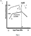
- Fig. 5 shows examples of backscattering versus input power curves 500.
- a transponder will typically be supplied with power through the field generated by the reader (which may also be referred to as an interrogator). This field is used to generate the local internal chip supply.
- the transponder typically responds to the reader by modulating this field, for example through a switch, which is usually an NMOS device. This process may also be referred to as backscattering.
- the strength of the backscatter depends on the gate voltage of the switch and the size of the switch. If the gate voltage is set to a maximum, then the strength of the backscatter will only be dependent on the size of this switch.
- the switch will have to be changed if the backscatter strength should be adjusted, for example to meet certain predefined requirements.
- the gate voltage of the NMOS switch may be varied in dependence on the strength of the input field. In this way, the backscatter strength may easily be adjusted. This may be necessary to meet requirements defined, for example, by the European Telecommunications Standards Institute (ETSI).
- ETSI European Telecommunications Standards Institute
- the backscatter strength and hence the electromagnetic interference (EMI) should be reduced at higher input power levels (for example -20dBm at +18dBm).
- EMI electromagnetic interference
- a maximum backscatter strength is required.
- a maximum backscattering versus input power curve 502 a backscattering versus input power according to predefined requirements curve 504 (i.e., a curve as should be achieved to meet predefined requirements such as the aforementioned ETSI requirements, and a backscattering versus input power curve after scaling down NMOS switch 506.
- predefined requirements curve 504 i.e., a curve as should be achieved to meet predefined requirements such as the aforementioned ETSI requirements
- An adaptive control which is based on the strength of the input field facilitates achieving this curve.
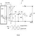
- Fig. 6 shows an illustrative embodiment of an adaptive modulation concept 600.
- the output of a shunt regulator 602 can be indicative of the strength of the input, more specifically of the amount of power available to the RFID transponder.
- the shunt regulator 602 may form part of a contactless front-end of the RFID transponder.
- the shunt regulator 602 is typically used to regulate the chip supply by shunting the excess current "I". Since the shunt current "I" has the characteristic that it increases proportionally with the input field strength, it is a suitable control parameter for an adaptive control of the kind set forth.
- a part of the shunt current can be mirrored by current mirror 608 to invert the characteristic using a resistor 606 to generate the gate voltage of the modulator switch 612.
- the controller is configured to sample the output of the shunt regulator 602 before the RFID transponder enters into a modulation phase. In this way, it may be ensured that the current can be mirrored during the modulation phase of the RFID transponder. In particular, the limiter current goes down during modulation, because all the current is shunted by the modulator switches 612 and 614. This problem may be overcome by sampling this current (and hence the voltage) on a sampling capacitor 610 before the modulation phase and by using this sampled voltage to drive the gate of the switch 612.
- Fig. 6 when the signal MOD is high, modulation takes place. Before modulation, i.e. when MOD_B is high, the limiter 602 current (and hence the voltage) is sampled on the sampling capacitor 610. During this phase switch 612 does not conduct. During the modulation phase, i.e. when MOD B is low and MOD is high, this sampled voltage is held by the sampling capacitor 610 and applied to the gate of the switch 612 which carries out the modulation.
- the minimum sampling capacitor size is determined by the instant charge to be provided to the parasitic gate capacitor of the switch 612 (and any logic in between, if any) and the longest modulation pulse duration.
- the maximum sampling capacitor is determined by the area limitation and time constant defined by sampling capacitor 610 and bias resistor 606 versus modulation period. Choosing a correct value of k and R can be used to achieve the ETSI specification at +18dBm. For example, by choosing a gate voltage which is less than the threshold of the switch 612, the backscatter strength can be reduced at 18 dBm and above, where only the switch 614 stays active during modulation.
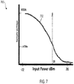
- Fig. 7 shows an illustrative embodiment of a sampled gate voltage 700.
- a curve 702 is shown which represents the sampled gate voltage versus the input power.
- the sampled gate voltage is less than the threshold of the switch 612 (VTHn) at 18 dBm and above.
- Fig. 8 shows examples of simulation results 800.
- curve 802 represents a simulation result without adaptive modulation
- curve 804 represents a simulation result with adaptive modulation in accordance with the present disclosure.
- curve 804 is similar to the desired curve 504 shown in Fig. 5 .
- predefined requirements e.g., ETSI requirements
- Fig. 9 shows a further illustrative embodiment of an RFID transponder 900.
- the RFID transponder comprises a controller 902, a voltage domain 904 and a level shifter 906.
- Fig. 9 shows one possible implementation that uses a level shifter 906 (which may also be referred to as a voltage level translator) for changing the control voltage of the modulator.
- the controller 902 is configured to adjust the backscatter strength by switching the voltage domain 904 of said voltage level converter 906.
- Fig. 10 shows a diagram 1000 which illustrates the impact of the changed level shifter voltage on the backscatter signal.
- Fig. 10 shows that the voltage level used by the level shifter can be used for changing the strength of the backscatter signal.
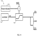
- Fig. 11 shows a further illustrative embodiment of an RFID transponder 1100.
- the RFID transponder 1100 comprises a controller 1102 and a level shifter 1106.
- Fig. 11 shows an implementation in which the level of the level shifter 1106 is changed using a power indicator 1104.
- This power indicator 1104 changes the voltage of the level shifter 1106 dynamically and adaptively, thereby also changing the strength of the backscatter signal.
Landscapes
- Engineering & Computer Science (AREA)
- Physics & Mathematics (AREA)
- Microelectronics & Electronic Packaging (AREA)
- Computer Hardware Design (AREA)
- Theoretical Computer Science (AREA)
- General Physics & Mathematics (AREA)
- Toxicology (AREA)
- Health & Medical Sciences (AREA)
- Computer Networks & Wireless Communication (AREA)
- Electromagnetism (AREA)
- Computer Vision & Pattern Recognition (AREA)
- Artificial Intelligence (AREA)
- General Health & Medical Sciences (AREA)
- Near-Field Transmission Systems (AREA)
Abstract
Description
- The present disclosure relates to a radio frequency identification transponder. Furthermore, the present disclosure relates to a method of operating a radio frequency identification transponder.
- Nowadays, radio frequency identification (RFID) transponders are widely used, in different areas of industry and commerce and for various purposes. RFID transponders may for example be embodied as so-called RFID tags or RFID cards. It is noted that, in the present disclosure, near field communication (NFC) transponders are regarded as a specific type of RFID transponders. Thus, the principles described herein may also be applied to NFC transponders.
- In accordance with a first aspect of the present disclosure, a radio frequency identification (RFID) transponder is provided, comprising a modulator and a controller, wherein: the modulator is configured to generate a modulated signal to be transmitted to an external RFID reader; the controller is configured to regulate an input voltage for the modulator, resulting in a regulated input voltage, and to feed said regulated input voltage to the modulator.
- In one or more embodiments, the controller is configured to regulate the input voltage in dependence on a power indicator, said power indicator being indicative of an amount of power available in the RFID transponder.
- In one or more embodiments, the controller is configured to regulate the input voltage in dependence on at least one of: an operating mode of the RFID transponder, an application domain in which the RFID transponder is used, a configuration of the RFID transponder, and parameters stored in the RFID transponder.
- In one or more embodiments, the controller is configured to control a voltage level translator, wherein said voltage level translator is configured to combine the regulated input voltage with a modulator control signal, to generate a regulated control signal for the modulator.
- In one or more embodiments, the modulator comprises an n-channel metal-oxide semiconductor (NMOS) switch, and said input voltage is the gate voltage of said NMOS switch.
- In one or more embodiments, the RFID transponder further comprises a shunt regulator, wherein the controller is configured to use an output of said shunt regulator for regulating the gate voltage.
- In one or more embodiments, the RFID transponder further comprises a current mirror, wherein said current mirror is configured to generate the gate voltage.
- In one or more embodiments, the controller is configured to sample the output of the shunt regulator before the RFID transponder enters into a modulation phase.
- In one or more embodiments, the RFID transponder is an RFID tag or an RFID card.
- In accordance with a second aspect of the present disclosure, a method of operating a radio frequency identification (RFID) transponder is conceived, the RFID transponder comprising a modulator and a controller, the method comprising: the controller regulates an input voltage for the modulator, resulting in a regulated input voltage, and feeds said regulated input voltage to the modulator; the modulator generates a modulated signal to be transmitted to an external RFID reader.
- In one or more embodiments, the controller regulates the input voltage in dependence on a power indicator, said power indicator being indicative of an amount of power available in the RFID transponder.
- In one or more embodiments, the controller regulates the input voltage in dependence on at least one of: an operating mode of the RFID transponder, an application domain in which the RFID transponder is used, a configuration of the RFID transponder, and parameters stored in the RFID transponder.
- In one or more embodiments, the controller controls a voltage level translator, wherein said voltage level translator combines the regulated input voltage with a modulator control signal, to generate a regulated control signal for the modulator.
- In one or more embodiments, the modulator comprises an n-channel metal-oxide semiconductor (NMOS) switch, and said input voltage is the gate voltage of said NMOS switch.
- In one or more embodiments, the RFID transponder further comprises a shunt regulator, and the controller uses an output of said shunt regulator for regulating the gate voltage.
- Embodiments will be described in more detail with reference to the appended drawings, in which:
-
Fig. 1 shows an illustrative embodiment of an RFID transponder; -
Fig. 2 shows an illustrative embodiment of a method of operating an RFID transponder; -
Fig. 3 shows an illustrative embodiment of a communication system; -
Fig. 4 shows another illustrative embodiment of an RFID transponder; -
Fig. 5 shows examples of backscattering versus input power curves; -
Fig. 6 shows an illustrative embodiment of an adaptive modulation concept; -
Fig. 7 shows an illustrative embodiment of a sampled gate voltage; -
Fig. 8 shows examples of simulation results; -
Fig. 9 shows a further illustrative embodiment of an RFID transponder; -
Fig. 10 shows a diagram which illustrates the impact of the changed level shifter voltage on the backscatter signal; -
Fig. 11 shows a further illustrative embodiment of an RFID transponder. - Nowadays, radio frequency identification (RFID) transponders are widely used, in different areas of industry and commerce and for various purposes. RFID transponders may for example be embodied as so-called RFID tags or RFID cards. It is noted that, in the present disclosure, near field communication (NFC) transponders are regarded as a specific type of RFID transponders. Thus, the principles described herein may also be applied to NFC transponders.
- RFID communication may be based on inductive coupling. The communication between an RFID reader and an RFID transponder, such as an RFID tag, is often realized by means of load modulation and can be split into a forward link and a return link. More specifically, the RFID reader may transmit commands to the RFID transponder through a forward link, and the RFID transponder may transmit responses to those commands back to the RFID reader through a return link. The RFID transponder contains a modulator, which load modulates a carrier signal. Different types of load modulation exist, for example active load modulation (ALM) and passive load modulation (PLM). The return link may also be referred to as a backscatter signal or more concisely as "backscatter".
- In RFID applications the return link is an important parameter. In RFID transponders this backscatter is generated by a modulator, which includes one or more modulation transistors. The voltage that drives this modulator typically has a fixed level or a fixed voltage domain, and therefore the backscatter strength is defined. However, the different applications of RFID often require different backscatter strengths. Such application-related requirements are often defined in regulations issued by regulatory authorities. Since these requirements may also be subject to change, the backscatter strength of an RFID transponder should be easily adjustable. Furthermore, it would be advantageous if an RFID transponder can be used for various applications, and not only for a single application or a limited number of applications. Also for this reason, the backscatter strength of an RFID transponder should be easily adjustable. Adjusting the backscatter strength of an RFID transponder typically requires that the modulator is changed. However, it may be difficult and costly to change the modulator. Now discussed are an RFID transponder and a corresponding method of operating an RFID transponder, which facilitate adjusting the backscatter strength.
-
Fig. 1 shows an illustrative embodiment of a radio frequency identification (RFID) transponder. TheRFID transponder 100 includes amodulator 102 controlled by acontroller 104. Themodulator 102 is configured to generate a modulated signal to be transmitted to an external RFID reader (not shown). Furthermore, thecontroller 104 is configured to regulate an input voltage for the modulator, which results in a regulated input voltage. Furthermore, thecontroller 104 is configured to feed the regulated input voltage to the modulator. In this way, the strength of the return link can easily be adjusted. -
Fig. 2 shows an illustrative embodiment of amethod 200 of operating an RFID transponder. Themethod 200 comprises the following steps. At 202, a controller regulates an input voltage for a modulator and feeds the regulated input voltage to the modulator. Furthermore, at 204, the modulator generates a modulator signal to be transmitted to an external RFID reader. In this way, the strength of the return link can easily be adjusted. -
Fig. 3 shows an illustrative embodiment of anRFID communication system 300 in which theRFID transponder 100 is used. Thecommunication system 300 comprises anRFID transponder 100 of the kind set forth and anRFID reader 302 which communicate with each other. TheRFID transponder 100 includes themodulator 102 which is controlled by thecontroller 104. Similarly, theRFID reader 302 includes ademodulator 304 which is controlled by acontroller 306. In operation, theRFID transponder 100 modulates a carrier wave generated by theRFID reader 302, resulting in a modulated signal, and transmits the modulated signal to theRFID reader 302. TheRFID reader 302 receives said modulated signal and demodulates it using thedemodulator 304. In accordance with the present disclosure, thecontroller 104 is configured to regulate an input voltage for the modulator, which results in a regulated input voltage. Furthermore, thecontroller 104 is configured to feed the regulated input voltage to the modulator. - In an embodiment, the controller is configured to regulate the input voltage in dependence on a power indicator, wherein said power indicator is indicative of an amount of power available in the RFID transponder. Thus, according to the available power, the backscatter strength may be adapted to fulfil national regulations, by changing the voltage used to control the modulator. To reduce the backscatter strength, a lower input voltage may be fed to the modulator. On the other hand, if the available amount of power is low, then the backscatter strength may be increased to increase the system performance. To increase the backscatter strength, a higher input voltage may be fed to the modulator. Thus, in this context, voltage regulation refers to an adjustment of the input voltage of the modulator.
- In an embodiment, the controller is configured to regulate the input voltage in dependence on an operating mode of the RFID transponder. For example, the operating mode may be a production mode, a certification mode, and an application mode of the RFID transponder. In this way, the backscatter strength can easily be adjusted to accommodate different operating conditions of the RFID transponder. Furthermore, in an embodiment, the controller is configured to regulate the input voltage in dependence on an application domain in which the RFID transponder is used. In this way, the backscatter strength can easily be adjusted to meet specific application-related requirements. In a further embodiment, the controller is configured to regulate the input voltage in dependence on a configuration of the RFID transponder. In this way, the backscatter strength can easily be adjusted in accordance with the configuration of the RFID transponder. For example, the configuration may be a setting that sets the modulator in one of the available operating modes. This setting may be stored in a memory of the RFID transponder. In a further embodiment, the controller is configured to regulate the input voltage in dependence on parameters stored in the RFID transponder. For example, the application domain and the configuration are parameters which may be stored in the RFID transponder. This enables an easy update of the parameters, which in turn results in an easy reconfiguration of the RFID transponder and/or the possibility of reusing the RFID transponder in another application domain.
-
Fig. 4 shows another illustrative embodiment of anRFID transponder 400. In particular, an example is shown of an implementation of the RFID transponder shown inFig. 1 . TheRFID transponder 400 comprises amodulator 402, avoltage regulator 404, avoltage level translator 414 and a plurality ofvoltage domains voltage regulator 404 forms part of a controller of the kind set forth. Furthermore, thevoltage level translator 414 may be controlled by a controller of the kind set forth. In some implementations, thevoltage level translator 414 may also form part of the controller. In a practical and effective implementation, thevoltage level translator 414 is configured to combine the regulated input voltage - i.e., the voltage output by the voltage regulator 404 - with amodulator signal 416. This may be done by changing the amplitude of the modulator signal. It is noted that the voltage level translator may also be referred to as a level shifter. Themodulator signal 416 may also be generated and provided by the controller. The output of thevoltage level translator 414 is an adjusted modulator control signal, which depends on the input voltage provided by thevoltage regulator 404. The adjusted modulator control signal is fed to the modulator. Thevoltage regulator 404 may regulate the input voltage for themodulator 402 in dependence on apower indicator 406 and/or a mode ofoperation 412. The power indicator may be indicative of the available amount of power in the RFID transponder, for example of the amount of power extracted from the field through RFp and RFn pins connected to the transponder's antenna (not shown). To regulate the input voltage for themodulator 402, thevoltage regulator 404 may be connectable todifferent voltage domains 408, 410 (i.e., power domains). By connecting thevoltage regulator 404 to a givenvoltage domain voltage level translator 414. A voltage domain has a given voltage supply level, which may be output by a charge pump or which may be generated within the integrated circuit for supplying power to other components. - In one or more embodiments, the modulator comprises an n-channel metal-oxide semiconductor (NMOS) switch, and said input voltage is the gate voltage of said NMOS switch. This results in a practical and effective implementation of the modulator. Furthermore, in this way, the backscatter strength can easily be adjusted. In one or more embodiments, the RFID transponder further comprises a shunt regulator, and the controller is configured to use an output of said shunt regulator for regulating the gate voltage. The shunt regulator may be included in a contactless front-end of the RFID transponder. The output of the shunt regulator provides a suitable indication of the amount of power available in the RFID transponder. Thus, in this way, the input voltage can easily be regulated in dependence on the available amount of power. Furthermore, in one or more embodiments, the RFID transponder comprises a current mirror which is configured to generate the gate voltage. This results in a practical and effective implementation. Furthermore, in one or more embodiments, the controller is configured to sample the output of the shunt regulator before the RFID transponder enters into a modulation phase. In this way, as will be explained in more detail hereinbelow, it is ensured that the current can be mirrored during the modulation phase of the RFID transponder.
-
Fig. 5 shows examples of backscattering versus input power curves 500. During normal communication a transponder will typically be supplied with power through the field generated by the reader (which may also be referred to as an interrogator). This field is used to generate the local internal chip supply. The transponder typically responds to the reader by modulating this field, for example through a switch, which is usually an NMOS device. This process may also be referred to as backscattering. In this example, the strength of the backscatter depends on the gate voltage of the switch and the size of the switch. If the gate voltage is set to a maximum, then the strength of the backscatter will only be dependent on the size of this switch. As a result, the switch will have to be changed if the backscatter strength should be adjusted, for example to meet certain predefined requirements. In accordance with the present disclosure, the gate voltage of the NMOS switch may be varied in dependence on the strength of the input field. In this way, the backscatter strength may easily be adjusted. This may be necessary to meet requirements defined, for example, by the European Telecommunications Standards Institute (ETSI). In order to meet ETSI requirements the backscatter strength and hence the electromagnetic interference (EMI) should be reduced at higher input power levels (for example -20dBm at +18dBm). In contrast, at low input powers levels (for example -22dBm to 0dBm) a maximum backscatter strength is required. With a constant gate voltage and size of the NMOS switch it is not possible to reduce the EMI at and above one point and achieve a maximum backscatter strength at lower input power levels. - This problem is illustrated in
Fig. 5 , wherein three curves are shown: a maximum backscattering versusinput power curve 502, a backscattering versus input power according to predefined requirements curve 504 (i.e., a curve as should be achieved to meet predefined requirements such as the aforementioned ETSI requirements, and a backscattering versus input power curve after scaling downNMOS switch 506. In particular, to avoid negatively affecting the backscatter strength at lower input power levels it would be necessary to achievecurve 504. An adaptive control which is based on the strength of the input field facilitates achieving this curve. -
Fig. 6 shows an illustrative embodiment of anadaptive modulation concept 600. The output of ashunt regulator 602 can be indicative of the strength of the input, more specifically of the amount of power available to the RFID transponder. Theshunt regulator 602 may form part of a contactless front-end of the RFID transponder. Theshunt regulator 602 is typically used to regulate the chip supply by shunting the excess current "I". Since the shunt current "I" has the characteristic that it increases proportionally with the input field strength, it is a suitable control parameter for an adaptive control of the kind set forth. Furthermore, a part of the shunt current can be mirrored by current mirror 608 to invert the characteristic using aresistor 606 to generate the gate voltage of themodulator switch 612. This inverted characteristic can be represented by the equation Vg = VDDA - I∗k∗R, where VDDA represents the internal chip supply, I represents the limiter current, k represents the scaling factor and R represents the bias resistor used to invert the characteristic. - As mentioned above, in one or more embodiments, the controller is configured to sample the output of the
shunt regulator 602 before the RFID transponder enters into a modulation phase. In this way, it may be ensured that the current can be mirrored during the modulation phase of the RFID transponder. In particular, the limiter current goes down during modulation, because all the current is shunted by the modulator switches 612 and 614. This problem may be overcome by sampling this current (and hence the voltage) on asampling capacitor 610 before the modulation phase and by using this sampled voltage to drive the gate of theswitch 612. - In
Fig. 6 , when the signal MOD is high, modulation takes place. Before modulation, i.e. when MOD_B is high, thelimiter 602 current (and hence the voltage) is sampled on thesampling capacitor 610. During thisphase switch 612 does not conduct. During the modulation phase, i.e. when MOD B is low and MOD is high, this sampled voltage is held by thesampling capacitor 610 and applied to the gate of theswitch 612 which carries out the modulation. The minimum sampling capacitor size is determined by the instant charge to be provided to the parasitic gate capacitor of the switch 612 (and any logic in between, if any) and the longest modulation pulse duration. The maximum sampling capacitor is determined by the area limitation and time constant defined by samplingcapacitor 610 andbias resistor 606 versus modulation period. Choosing a correct value of k and R can be used to achieve the ETSI specification at +18dBm. For example, by choosing a gate voltage which is less than the threshold of theswitch 612, the backscatter strength can be reduced at 18 dBm and above, where only theswitch 614 stays active during modulation. -
Fig. 7 shows an illustrative embodiment of a sampledgate voltage 700. In particular, acurve 702 is shown which represents the sampled gate voltage versus the input power. As shown, the sampled gate voltage is less than the threshold of the switch 612 (VTHn) at 18 dBm and above. -
Fig. 8 shows examples of simulation results 800. In particular,curve 802 represents a simulation result without adaptive modulation, whilecurve 804 represents a simulation result with adaptive modulation in accordance with the present disclosure. As shown,curve 804 is similar to the desiredcurve 504 shown inFig. 5 . Thus, by using the adaptive modulation, predefined requirements (e.g., ETSI requirements) can be met. -
Fig. 9 shows a further illustrative embodiment of anRFID transponder 900. The RFID transponder comprises acontroller 902, avoltage domain 904 and alevel shifter 906. In particular,Fig. 9 shows one possible implementation that uses a level shifter 906 (which may also be referred to as a voltage level translator) for changing the control voltage of the modulator. Thecontroller 902 is configured to adjust the backscatter strength by switching thevoltage domain 904 of saidvoltage level converter 906. -
Fig. 10 shows a diagram 1000 which illustrates the impact of the changed level shifter voltage on the backscatter signal. In particular,Fig. 10 shows that the voltage level used by the level shifter can be used for changing the strength of the backscatter signal. -
Fig. 11 shows a further illustrative embodiment of anRFID transponder 1100. TheRFID transponder 1100 comprises acontroller 1102 and alevel shifter 1106. In particular,Fig. 11 shows an implementation in which the level of thelevel shifter 1106 is changed using apower indicator 1104. Thispower indicator 1104 changes the voltage of thelevel shifter 1106 dynamically and adaptively, thereby also changing the strength of the backscatter signal. - It is noted that the embodiments above have been described with reference to different subject-matters. In particular, some embodiments may have been described with reference to method-type claims whereas other embodiments may have been described with reference to apparatus-type claims. However, a person skilled in the art will gather from the above that, unless otherwise indicated, in addition to any combination of features belonging to one type of subject-matter also any combination of features relating to different subject-matters, in particular a combination of features of the method-type claims and features of the apparatus-type claims, is considered to be disclosed with this document.
- Furthermore, it is noted that the drawings are schematic. In different drawings, similar or identical elements are provided with the same reference signs. Furthermore, it is noted that in an effort to provide a concise description of the illustrative embodiments, implementation details which fall into the customary practice of the skilled person may not have been described. It should be appreciated that in the development of any such implementation, as in any engineering or design project, numerous implementation-specific decisions must be made in order to achieve the developers' specific goals, such as compliance with system-related and business-related constraints, which may vary from one implementation to another. Moreover, it should be appreciated that such a development effort might be complex and time consuming, but would nevertheless be a routine undertaking of design, fabrication, and manufacture for those of ordinary skill.
- Finally, it is noted that the skilled person will be able to design many alternative embodiments without departing from the scope of the appended claims. In the claims, any reference sign placed between parentheses shall not be construed as limiting the claim. The word "comprise(s)" or "comprising" does not exclude the presence of elements or steps other than those listed in a claim. The word "a" or "an" preceding an element does not exclude the presence of a plurality of such elements. Measures recited in the claims may be implemented by means of hardware comprising several distinct elements and/or by means of a suitably programmed processor. In a device claim enumerating several means, several of these means maybe embodied by one and the same item of hardware. The mere fact that certain measures are recited in mutually different dependent claims does not indicate that a combination of these measures cannot be used to advantage.
-
- 100
- RFID transponder
- 102
- modulator
- 104
- controller
- 200
- method of operating an RFID transponder
- 202
- controller regulates an input voltage for a modulator and feeds the regulated input voltage to the modulator
- 204
- modulator generates a modulated signal to be transmitted to an external RFID reader
- 300
- communication system
- 302
- RFID reader
- 304
- demodulator
- 306
- controller
- 400
- RFID transponder
- 402
- modulator
- 404
- voltage regulator
- 406
- power indicator
- 408
-
voltage domain 1 - 410
- voltage domain n
- 412
- mode of operation
- 414
- voltage level translator
- 416
- modulator signal
- 500
- backscattering versus input power
- 502
- maximum backscattering versus input power
- 504
- backscattering versus input power according to requirements
- 506
- backscattering versus input power after scaling down NMOS switch
- 600
- adaptive modulation concept
- 602
- shunt regulator or limiter
- 604
- inverter
- 606
- bias resistor
- 608
- current mirror
- 610
- sampling capacitor
- 612
- modulator switch
- 614
- modulator switch
- 700
- sampled gate voltage
- 702
- sampled gate voltage versus input power
- 800
- simulation results
- 802
- simulation result without adaptive modulation
- 804
- simulation result with adaptive modulation
- 900
- RFID transponder
- 902
- controller
- 904
- voltage domain
- 906
- level shifter
- 1000
- impact of the changed level shifter voltage on the backscatter signal
- 1100
- RFID transponder
- 1102
- controller
- 1104
- power indicator
- 1106
- level shifter
Claims (15)
- A radio frequency identification, RFID, transponder, comprising a modulator and a controller, wherein:the modulator is configured to generate a modulated signal to be transmitted to an external RFID reader;the controller is configured to regulate an input voltage for the modulator, resulting in a regulated input voltage, and to feed said regulated input voltage to the modulator.
- The RFID transponder of claim 1, wherein the controller is configured to regulate the input voltage in dependence on a power indicator, said power indicator being indicative of an amount of power available in the RFID transponder.
- The RFID transponder of any preceding claim, wherein the controller is configured to regulate the input voltage in dependence on at least one of: an operating mode of the RFID transponder, an application domain in which the RFID transponder is used, a configuration of the RFID transponder, and parameters stored in the RFID transponder.
- The RFID transponder of any preceding claim, wherein the controller is configured to control a voltage level translator, wherein said voltage level translator is configured to combine the regulated input voltage with a modulator control signal, to generate a regulated control signal for the modulator.
- The RFID transponder of any preceding claim, wherein the modulator comprises an n-channel metal-oxide semiconductor (NMOS) switch, and wherein said input voltage is the gate voltage of said NMOS switch.
- The RFID transponder of claim 5, further comprising a shunt regulator, wherein the controller is configured to use an output of said shunt regulator for regulating the gate voltage.
- The RFID transponder of claim 5 or 6, further comprising a current mirror, wherein said current mirror is configured to generate the gate voltage.
- The RFID transponder of claim 6 and 7, wherein the controller is configured to sample the output of the shunt regulator before the RFID transponder enters into a modulation phase.
- The RFID transponder of any preceding claim, being an RFID tag or an RFID card.
- A method of operating a radio frequency identification, RFID, transponder, the RFID transponder comprising a modulator and a controller, the method comprising:the controller regulates an input voltage for the modulator, resulting in a regulated input voltage, and feeds said regulated input voltage to the modulator;the modulator generates a modulated signal to be transmitted to an external RFID reader.
- The method of claim 10, wherein the controller regulates the input voltage in dependence on a power indicator, said power indicator being indicative of an amount of power available in the RFID transponder.
- The method of claim 10 or 11, wherein the controller regulates the input voltage in dependence on at least one of: an operating mode of the RFID transponder, an application domain in which the RFID transponder is used, a configuration of the RFID transponder, and parameters stored in the RFID transponder.
- The method of any one of claims 10 to 12, wherein the controller controls a voltage level translator, wherein said voltage level translator combines the regulated input voltage with a modulator control signal, to generate a regulated control signal for the modulator.
- The method of any preceding claim, wherein the modulator comprises an n-channel metal-oxide semiconductor (NMOS) switch, and wherein said input voltage is the gate voltage of said NMOS switch.
- The method of claim 14, wherein the RFID transponder further comprises a shunt regulator, and wherein the controller uses an output of said shunt regulator for regulating the gate voltage.
Priority Applications (3)
| Application Number | Priority Date | Filing Date | Title |
|---|---|---|---|
| EP19206721.3A EP3816860B1 (en) | 2019-11-01 | 2019-11-01 | Rfid transponder and method of operating an rfid transponder |
| US17/065,582 US11164062B2 (en) | 2019-11-01 | 2020-10-08 | RFID transponder and method of operating an RFID transponder |
| CN202011091392.9A CN112784618B (en) | 2019-11-01 | 2020-10-13 | RFID transponder and method for operating an RFID transponder |
Applications Claiming Priority (1)
| Application Number | Priority Date | Filing Date | Title |
|---|---|---|---|
| EP19206721.3A EP3816860B1 (en) | 2019-11-01 | 2019-11-01 | Rfid transponder and method of operating an rfid transponder |
Publications (2)
| Publication Number | Publication Date |
|---|---|
| EP3816860A1 true EP3816860A1 (en) | 2021-05-05 |
| EP3816860B1 EP3816860B1 (en) | 2023-01-18 |
Family
ID=68426203
Family Applications (1)
| Application Number | Title | Priority Date | Filing Date |
|---|---|---|---|
| EP19206721.3A Active EP3816860B1 (en) | 2019-11-01 | 2019-11-01 | Rfid transponder and method of operating an rfid transponder |
Country Status (3)
| Country | Link |
|---|---|
| US (1) | US11164062B2 (en) |
| EP (1) | EP3816860B1 (en) |
| CN (1) | CN112784618B (en) |
Citations (4)
| Publication number | Priority date | Publication date | Assignee | Title |
|---|---|---|---|---|
| US20030183699A1 (en) * | 2002-03-29 | 2003-10-02 | Fujitsu Limited | Semiconductor integrated circuit, radio frequency identification transponder, and non-cotact IC card |
| US20050052279A1 (en) * | 2003-08-29 | 2005-03-10 | Raj Bridgelall | RFID system with selectable backscatter parameters |
| US20170061172A1 (en) * | 2015-08-24 | 2017-03-02 | Ruizhang Technology Limited Company | Increasing backscatter level for rfid chip |
| EP3416088A1 (en) * | 2017-06-14 | 2018-12-19 | Intermec Inc. | Method to increase rfid tag sensitivity |
Family Cites Families (11)
| Publication number | Priority date | Publication date | Assignee | Title |
|---|---|---|---|---|
| US20050140457A1 (en) * | 2003-12-31 | 2005-06-30 | Wj Communications, Inc. | Linearized power amplifier modulator in an RFID reader |
| US7990249B1 (en) | 2006-08-03 | 2011-08-02 | Impinj, Inc. | RFID tag circuits tags and methods for backscattering with controllable admittance |
| DE102007004843A1 (en) | 2007-01-31 | 2008-08-07 | Infineon Technologies Ag | Concept for providing a supply voltage and a load modulation in a transponder |
| GB0722516D0 (en) * | 2007-11-15 | 2007-12-27 | Innovision Res & Tech Plc | Near field communication devices |
| AU2011265835B2 (en) | 2010-06-11 | 2016-08-25 | Trident Rfid Pty Ltd | A transponder, RFID system and methods of operation |
| US8472887B2 (en) * | 2010-09-09 | 2013-06-25 | The United States Of America As Represented By The Secretary Of The Army | Radio frequency integrated circuit for enhanced transmit/receive performance in low power applications and method of making the same |
| DE102011016027A1 (en) * | 2011-04-04 | 2012-10-04 | Markus Rehm | Large signal VCO |
| US9070062B2 (en) | 2011-07-11 | 2015-06-30 | Square, Inc. | Streamlined apparatus and methods for RFID communication |
| JP6804364B2 (en) * | 2017-03-29 | 2020-12-23 | 富士通セミコンダクターメモリソリューション株式会社 | Rectifier circuit and electronic device |
| EP3457580B1 (en) * | 2017-09-19 | 2020-02-19 | Nxp B.V. | Nfc controller |
| US10228714B1 (en) * | 2018-05-25 | 2019-03-12 | Lite-On Singapore Pte. Ltd. | Low dropout shunt voltage regulator with wide input supply voltage range |
-
2019
- 2019-11-01 EP EP19206721.3A patent/EP3816860B1/en active Active
-
2020
- 2020-10-08 US US17/065,582 patent/US11164062B2/en active Active
- 2020-10-13 CN CN202011091392.9A patent/CN112784618B/en active Active
Patent Citations (4)
| Publication number | Priority date | Publication date | Assignee | Title |
|---|---|---|---|---|
| US20030183699A1 (en) * | 2002-03-29 | 2003-10-02 | Fujitsu Limited | Semiconductor integrated circuit, radio frequency identification transponder, and non-cotact IC card |
| US20050052279A1 (en) * | 2003-08-29 | 2005-03-10 | Raj Bridgelall | RFID system with selectable backscatter parameters |
| US20170061172A1 (en) * | 2015-08-24 | 2017-03-02 | Ruizhang Technology Limited Company | Increasing backscatter level for rfid chip |
| EP3416088A1 (en) * | 2017-06-14 | 2018-12-19 | Intermec Inc. | Method to increase rfid tag sensitivity |
Also Published As
| Publication number | Publication date |
|---|---|
| US20210133526A1 (en) | 2021-05-06 |
| US11164062B2 (en) | 2021-11-02 |
| CN112784618B (en) | 2025-12-19 |
| CN112784618A (en) | 2021-05-11 |
| EP3816860B1 (en) | 2023-01-18 |
Similar Documents
| Publication | Publication Date | Title |
|---|---|---|
| US11960955B1 (en) | Fast frequency switching for RFID applications | |
| US10566841B2 (en) | Wireless power supply device, wireless power receiving device, wireless power transmission system, and wireless power supply method | |
| CN109039387B (en) | Method for monitoring power level and corresponding contactless communication device | |
| US20250348701A1 (en) | Smart card | |
| US11270177B2 (en) | RFID transponder and corresponding operating method | |
| US11164062B2 (en) | RFID transponder and method of operating an RFID transponder | |
| US11023797B2 (en) | RFID transponder and method of operating the same | |
| US20160119033A1 (en) | Method for Operating Object Capable via Contactless Communication | |
| JP6529919B2 (en) | Wireless transmission apparatus and method | |
| US11264838B2 (en) | Semiconductor device and semiconductor module | |
| CN107659282B (en) | Radio frequency voltage limiting method and device | |
| US11126906B2 (en) | Transponder and corresponding operating method | |
| US10984301B2 (en) | Method for limiting the level of a modulated signal received by a tag and corresponding limiter | |
| US11909426B2 (en) | Wave-shaping for over- and undershoot prevention | |
| GB2484104A (en) | Combined regulator and rectifier for a near field RF communicator | |
| WO2025141507A1 (en) | Rfid tag, rfid analog conditioner circuit and rfid tag digital core | |
| CN111030449B (en) | Switch mode power supply of NFC type reader-writer | |
| JP2025149692A (en) | Wireless communication circuit | |
| US10870010B2 (en) | DC-DC converter for implantable medical devices | |
| KR20030088233A (en) | Identification card and identification card system | |
| CN103544521A (en) | Contactless card modulation circuit |
Legal Events
| Date | Code | Title | Description |
|---|---|---|---|
| PUAI | Public reference made under article 153(3) epc to a published international application that has entered the european phase |
Free format text: ORIGINAL CODE: 0009012 |
|
| STAA | Information on the status of an ep patent application or granted ep patent |
Free format text: STATUS: THE APPLICATION HAS BEEN PUBLISHED |
|
| AK | Designated contracting states |
Kind code of ref document: A1 Designated state(s): AL AT BE BG CH CY CZ DE DK EE ES FI FR GB GR HR HU IE IS IT LI LT LU LV MC MK MT NL NO PL PT RO RS SE SI SK SM TR |
|
| STAA | Information on the status of an ep patent application or granted ep patent |
Free format text: STATUS: REQUEST FOR EXAMINATION WAS MADE |
|
| 17P | Request for examination filed |
Effective date: 20211105 |
|
| RBV | Designated contracting states (corrected) |
Designated state(s): AL AT BE BG CH CY CZ DE DK EE ES FI FR GB GR HR HU IE IS IT LI LT LU LV MC MK MT NL NO PL PT RO RS SE SI SK SM TR |
|
| GRAP | Despatch of communication of intention to grant a patent |
Free format text: ORIGINAL CODE: EPIDOSNIGR1 |
|
| STAA | Information on the status of an ep patent application or granted ep patent |
Free format text: STATUS: GRANT OF PATENT IS INTENDED |
|
| INTG | Intention to grant announced |
Effective date: 20221020 |
|
| GRAS | Grant fee paid |
Free format text: ORIGINAL CODE: EPIDOSNIGR3 |
|
| GRAA | (expected) grant |
Free format text: ORIGINAL CODE: 0009210 |
|
| STAA | Information on the status of an ep patent application or granted ep patent |
Free format text: STATUS: THE PATENT HAS BEEN GRANTED |
|
| AK | Designated contracting states |
Kind code of ref document: B1 Designated state(s): AL AT BE BG CH CY CZ DE DK EE ES FI FR GB GR HR HU IE IS IT LI LT LU LV MC MK MT NL NO PL PT RO RS SE SI SK SM TR |
|
| REG | Reference to a national code |
Ref country code: GB Ref legal event code: FG4D |
|
| REG | Reference to a national code |
Ref country code: CH Ref legal event code: EP |
|
| REG | Reference to a national code |
Ref country code: DE Ref legal event code: R096 Ref document number: 602019024506 Country of ref document: DE |
|
| REG | Reference to a national code |
Ref country code: AT Ref legal event code: REF Ref document number: 1545094 Country of ref document: AT Kind code of ref document: T Effective date: 20230215 Ref country code: IE Ref legal event code: FG4D |
|
| REG | Reference to a national code |
Ref country code: LT Ref legal event code: MG9D |
|
| REG | Reference to a national code |
Ref country code: NL Ref legal event code: MP Effective date: 20230118 |
|
| REG | Reference to a national code |
Ref country code: AT Ref legal event code: MK05 Ref document number: 1545094 Country of ref document: AT Kind code of ref document: T Effective date: 20230118 |
|
| PG25 | Lapsed in a contracting state [announced via postgrant information from national office to epo] |
Ref country code: NL Free format text: LAPSE BECAUSE OF FAILURE TO SUBMIT A TRANSLATION OF THE DESCRIPTION OR TO PAY THE FEE WITHIN THE PRESCRIBED TIME-LIMIT Effective date: 20230118 |
|
| PG25 | Lapsed in a contracting state [announced via postgrant information from national office to epo] |
Ref country code: RS Free format text: LAPSE BECAUSE OF FAILURE TO SUBMIT A TRANSLATION OF THE DESCRIPTION OR TO PAY THE FEE WITHIN THE PRESCRIBED TIME-LIMIT Effective date: 20230118 Ref country code: PT Free format text: LAPSE BECAUSE OF FAILURE TO SUBMIT A TRANSLATION OF THE DESCRIPTION OR TO PAY THE FEE WITHIN THE PRESCRIBED TIME-LIMIT Effective date: 20230518 Ref country code: NO Free format text: LAPSE BECAUSE OF FAILURE TO SUBMIT A TRANSLATION OF THE DESCRIPTION OR TO PAY THE FEE WITHIN THE PRESCRIBED TIME-LIMIT Effective date: 20230418 Ref country code: LV Free format text: LAPSE BECAUSE OF FAILURE TO SUBMIT A TRANSLATION OF THE DESCRIPTION OR TO PAY THE FEE WITHIN THE PRESCRIBED TIME-LIMIT Effective date: 20230118 Ref country code: LT Free format text: LAPSE BECAUSE OF FAILURE TO SUBMIT A TRANSLATION OF THE DESCRIPTION OR TO PAY THE FEE WITHIN THE PRESCRIBED TIME-LIMIT Effective date: 20230118 Ref country code: HR Free format text: LAPSE BECAUSE OF FAILURE TO SUBMIT A TRANSLATION OF THE DESCRIPTION OR TO PAY THE FEE WITHIN THE PRESCRIBED TIME-LIMIT Effective date: 20230118 Ref country code: ES Free format text: LAPSE BECAUSE OF FAILURE TO SUBMIT A TRANSLATION OF THE DESCRIPTION OR TO PAY THE FEE WITHIN THE PRESCRIBED TIME-LIMIT Effective date: 20230118 Ref country code: AT Free format text: LAPSE BECAUSE OF FAILURE TO SUBMIT A TRANSLATION OF THE DESCRIPTION OR TO PAY THE FEE WITHIN THE PRESCRIBED TIME-LIMIT Effective date: 20230118 |
|
| P01 | Opt-out of the competence of the unified patent court (upc) registered |
Effective date: 20230725 |
|
| PG25 | Lapsed in a contracting state [announced via postgrant information from national office to epo] |
Ref country code: SE Free format text: LAPSE BECAUSE OF FAILURE TO SUBMIT A TRANSLATION OF THE DESCRIPTION OR TO PAY THE FEE WITHIN THE PRESCRIBED TIME-LIMIT Effective date: 20230118 Ref country code: PL Free format text: LAPSE BECAUSE OF FAILURE TO SUBMIT A TRANSLATION OF THE DESCRIPTION OR TO PAY THE FEE WITHIN THE PRESCRIBED TIME-LIMIT Effective date: 20230118 Ref country code: IS Free format text: LAPSE BECAUSE OF FAILURE TO SUBMIT A TRANSLATION OF THE DESCRIPTION OR TO PAY THE FEE WITHIN THE PRESCRIBED TIME-LIMIT Effective date: 20230518 Ref country code: GR Free format text: LAPSE BECAUSE OF FAILURE TO SUBMIT A TRANSLATION OF THE DESCRIPTION OR TO PAY THE FEE WITHIN THE PRESCRIBED TIME-LIMIT Effective date: 20230419 Ref country code: FI Free format text: LAPSE BECAUSE OF FAILURE TO SUBMIT A TRANSLATION OF THE DESCRIPTION OR TO PAY THE FEE WITHIN THE PRESCRIBED TIME-LIMIT Effective date: 20230118 |
|
| REG | Reference to a national code |
Ref country code: DE Ref legal event code: R097 Ref document number: 602019024506 Country of ref document: DE |
|
| PG25 | Lapsed in a contracting state [announced via postgrant information from national office to epo] |
Ref country code: SM Free format text: LAPSE BECAUSE OF FAILURE TO SUBMIT A TRANSLATION OF THE DESCRIPTION OR TO PAY THE FEE WITHIN THE PRESCRIBED TIME-LIMIT Effective date: 20230118 Ref country code: RO Free format text: LAPSE BECAUSE OF FAILURE TO SUBMIT A TRANSLATION OF THE DESCRIPTION OR TO PAY THE FEE WITHIN THE PRESCRIBED TIME-LIMIT Effective date: 20230118 Ref country code: EE Free format text: LAPSE BECAUSE OF FAILURE TO SUBMIT A TRANSLATION OF THE DESCRIPTION OR TO PAY THE FEE WITHIN THE PRESCRIBED TIME-LIMIT Effective date: 20230118 Ref country code: DK Free format text: LAPSE BECAUSE OF FAILURE TO SUBMIT A TRANSLATION OF THE DESCRIPTION OR TO PAY THE FEE WITHIN THE PRESCRIBED TIME-LIMIT Effective date: 20230118 Ref country code: CZ Free format text: LAPSE BECAUSE OF FAILURE TO SUBMIT A TRANSLATION OF THE DESCRIPTION OR TO PAY THE FEE WITHIN THE PRESCRIBED TIME-LIMIT Effective date: 20230118 |
|
| PLBE | No opposition filed within time limit |
Free format text: ORIGINAL CODE: 0009261 |
|
| STAA | Information on the status of an ep patent application or granted ep patent |
Free format text: STATUS: NO OPPOSITION FILED WITHIN TIME LIMIT |
|
| PG25 | Lapsed in a contracting state [announced via postgrant information from national office to epo] |
Ref country code: SK Free format text: LAPSE BECAUSE OF FAILURE TO SUBMIT A TRANSLATION OF THE DESCRIPTION OR TO PAY THE FEE WITHIN THE PRESCRIBED TIME-LIMIT Effective date: 20230118 |
|
| 26N | No opposition filed |
Effective date: 20231019 |
|
| PG25 | Lapsed in a contracting state [announced via postgrant information from national office to epo] |
Ref country code: SI Free format text: LAPSE BECAUSE OF FAILURE TO SUBMIT A TRANSLATION OF THE DESCRIPTION OR TO PAY THE FEE WITHIN THE PRESCRIBED TIME-LIMIT Effective date: 20230118 |
|
| PG25 | Lapsed in a contracting state [announced via postgrant information from national office to epo] |
Ref country code: IT Free format text: LAPSE BECAUSE OF FAILURE TO SUBMIT A TRANSLATION OF THE DESCRIPTION OR TO PAY THE FEE WITHIN THE PRESCRIBED TIME-LIMIT Effective date: 20230118 |
|
| REG | Reference to a national code |
Ref country code: CH Ref legal event code: PL |
|
| PG25 | Lapsed in a contracting state [announced via postgrant information from national office to epo] |
Ref country code: MC Free format text: LAPSE BECAUSE OF FAILURE TO SUBMIT A TRANSLATION OF THE DESCRIPTION OR TO PAY THE FEE WITHIN THE PRESCRIBED TIME-LIMIT Effective date: 20230118 |
|
| PG25 | Lapsed in a contracting state [announced via postgrant information from national office to epo] |
Ref country code: LU Free format text: LAPSE BECAUSE OF NON-PAYMENT OF DUE FEES Effective date: 20231101 |
|
| PG25 | Lapsed in a contracting state [announced via postgrant information from national office to epo] |
Ref country code: CH Free format text: LAPSE BECAUSE OF NON-PAYMENT OF DUE FEES Effective date: 20231130 |
|
| GBPC | Gb: european patent ceased through non-payment of renewal fee |
Effective date: 20231101 |
|
| PG25 | Lapsed in a contracting state [announced via postgrant information from national office to epo] |
Ref country code: MC Free format text: LAPSE BECAUSE OF FAILURE TO SUBMIT A TRANSLATION OF THE DESCRIPTION OR TO PAY THE FEE WITHIN THE PRESCRIBED TIME-LIMIT Effective date: 20230118 Ref country code: LU Free format text: LAPSE BECAUSE OF NON-PAYMENT OF DUE FEES Effective date: 20231101 Ref country code: CH Free format text: LAPSE BECAUSE OF NON-PAYMENT OF DUE FEES Effective date: 20231130 |
|
| REG | Reference to a national code |
Ref country code: BE Ref legal event code: MM Effective date: 20231130 |
|
| REG | Reference to a national code |
Ref country code: IE Ref legal event code: MM4A |
|
| PG25 | Lapsed in a contracting state [announced via postgrant information from national office to epo] |
Ref country code: IE Free format text: LAPSE BECAUSE OF NON-PAYMENT OF DUE FEES Effective date: 20231101 |
|
| PG25 | Lapsed in a contracting state [announced via postgrant information from national office to epo] |
Ref country code: GB Free format text: LAPSE BECAUSE OF NON-PAYMENT OF DUE FEES Effective date: 20231101 |
|
| PG25 | Lapsed in a contracting state [announced via postgrant information from national office to epo] |
Ref country code: BE Free format text: LAPSE BECAUSE OF NON-PAYMENT OF DUE FEES Effective date: 20231130 |
|
| PG25 | Lapsed in a contracting state [announced via postgrant information from national office to epo] |
Ref country code: IE Free format text: LAPSE BECAUSE OF NON-PAYMENT OF DUE FEES Effective date: 20231101 Ref country code: GB Free format text: LAPSE BECAUSE OF NON-PAYMENT OF DUE FEES Effective date: 20231101 Ref country code: BE Free format text: LAPSE BECAUSE OF NON-PAYMENT OF DUE FEES Effective date: 20231130 |
|
| PG25 | Lapsed in a contracting state [announced via postgrant information from national office to epo] |
Ref country code: BG Free format text: LAPSE BECAUSE OF FAILURE TO SUBMIT A TRANSLATION OF THE DESCRIPTION OR TO PAY THE FEE WITHIN THE PRESCRIBED TIME-LIMIT Effective date: 20230118 |
|
| PG25 | Lapsed in a contracting state [announced via postgrant information from national office to epo] |
Ref country code: BG Free format text: LAPSE BECAUSE OF FAILURE TO SUBMIT A TRANSLATION OF THE DESCRIPTION OR TO PAY THE FEE WITHIN THE PRESCRIBED TIME-LIMIT Effective date: 20230118 |
|
| PG25 | Lapsed in a contracting state [announced via postgrant information from national office to epo] |
Ref country code: CY Free format text: LAPSE BECAUSE OF FAILURE TO SUBMIT A TRANSLATION OF THE DESCRIPTION OR TO PAY THE FEE WITHIN THE PRESCRIBED TIME-LIMIT; INVALID AB INITIO Effective date: 20191101 |
|
| PG25 | Lapsed in a contracting state [announced via postgrant information from national office to epo] |
Ref country code: HU Free format text: LAPSE BECAUSE OF FAILURE TO SUBMIT A TRANSLATION OF THE DESCRIPTION OR TO PAY THE FEE WITHIN THE PRESCRIBED TIME-LIMIT; INVALID AB INITIO Effective date: 20191101 |
|
| PG25 | Lapsed in a contracting state [announced via postgrant information from national office to epo] |
Ref country code: TR Free format text: LAPSE BECAUSE OF FAILURE TO SUBMIT A TRANSLATION OF THE DESCRIPTION OR TO PAY THE FEE WITHIN THE PRESCRIBED TIME-LIMIT Effective date: 20230118 |
|
| PGFP | Annual fee paid to national office [announced via postgrant information from national office to epo] |
Ref country code: DE Payment date: 20251022 Year of fee payment: 7 |
|
| PGFP | Annual fee paid to national office [announced via postgrant information from national office to epo] |
Ref country code: FR Payment date: 20251022 Year of fee payment: 7 |