EP3816687A1 - Waveguide, waveguide production method, and polarisation splitter using said waveguide - Google Patents
Waveguide, waveguide production method, and polarisation splitter using said waveguide Download PDFInfo
- Publication number
- EP3816687A1 EP3816687A1 EP19759632.3A EP19759632A EP3816687A1 EP 3816687 A1 EP3816687 A1 EP 3816687A1 EP 19759632 A EP19759632 A EP 19759632A EP 3816687 A1 EP3816687 A1 EP 3816687A1
- Authority
- EP
- European Patent Office
- Prior art keywords
- waveguide
- sections
- core material
- polarisation
- effective index
- Prior art date
- Legal status (The legal status is an assumption and is not a legal conclusion. Google has not performed a legal analysis and makes no representation as to the accuracy of the status listed.)
- Granted
Links
Images


Classifications
-
- G—PHYSICS
- G02—OPTICS
- G02B—OPTICAL ELEMENTS, SYSTEMS OR APPARATUS
- G02B6/00—Light guides; Structural details of arrangements comprising light guides and other optical elements, e.g. couplings
- G02B6/0001—Light guides; Structural details of arrangements comprising light guides and other optical elements, e.g. couplings specially adapted for lighting devices or systems
- G02B6/0011—Light guides; Structural details of arrangements comprising light guides and other optical elements, e.g. couplings specially adapted for lighting devices or systems the light guides being planar or of plate-like form
- G02B6/0033—Means for improving the coupling-out of light from the light guide
- G02B6/0056—Means for improving the coupling-out of light from the light guide for producing polarisation effects, e.g. by a surface with polarizing properties or by an additional polarizing elements
-
- G—PHYSICS
- G02—OPTICS
- G02B—OPTICAL ELEMENTS, SYSTEMS OR APPARATUS
- G02B5/00—Optical elements other than lenses
- G02B5/18—Diffraction gratings
- G02B5/1833—Diffraction gratings comprising birefringent materials
-
- G—PHYSICS
- G02—OPTICS
- G02B—OPTICAL ELEMENTS, SYSTEMS OR APPARATUS
- G02B6/00—Light guides; Structural details of arrangements comprising light guides and other optical elements, e.g. couplings
- G02B6/10—Light guides; Structural details of arrangements comprising light guides and other optical elements, e.g. couplings of the optical waveguide type
- G02B6/12—Light guides; Structural details of arrangements comprising light guides and other optical elements, e.g. couplings of the optical waveguide type of the integrated circuit kind
- G02B6/126—Light guides; Structural details of arrangements comprising light guides and other optical elements, e.g. couplings of the optical waveguide type of the integrated circuit kind using polarisation effects
-
- G—PHYSICS
- G02—OPTICS
- G02B—OPTICAL ELEMENTS, SYSTEMS OR APPARATUS
- G02B5/00—Optical elements other than lenses
- G02B5/30—Polarising elements
- G02B5/3083—Birefringent or phase retarding elements
-
- G—PHYSICS
- G02—OPTICS
- G02B—OPTICAL ELEMENTS, SYSTEMS OR APPARATUS
- G02B6/00—Light guides; Structural details of arrangements comprising light guides and other optical elements, e.g. couplings
- G02B6/02—Optical fibres with cladding with or without a coating
- G02B6/028—Optical fibres with cladding with or without a coating with core or cladding having graded refractive index
- G02B6/0288—Multimode fibre, e.g. graded index core for compensating modal dispersion
-
- G—PHYSICS
- G02—OPTICS
- G02B—OPTICAL ELEMENTS, SYSTEMS OR APPARATUS
- G02B6/00—Light guides; Structural details of arrangements comprising light guides and other optical elements, e.g. couplings
- G02B6/24—Coupling light guides
-
- G—PHYSICS
- G02—OPTICS
- G02B—OPTICAL ELEMENTS, SYSTEMS OR APPARATUS
- G02B6/00—Light guides; Structural details of arrangements comprising light guides and other optical elements, e.g. couplings
- G02B6/02—Optical fibres with cladding with or without a coating
- G02B6/02057—Optical fibres with cladding with or without a coating comprising gratings
- G02B6/02076—Refractive index modulation gratings, e.g. Bragg gratings
- G02B6/0208—Refractive index modulation gratings, e.g. Bragg gratings characterised by their structure, wavelength response
- G02B6/02085—Refractive index modulation gratings, e.g. Bragg gratings characterised by their structure, wavelength response characterised by the grating profile, e.g. chirped, apodised, tilted, helical
-
- G—PHYSICS
- G02—OPTICS
- G02B—OPTICAL ELEMENTS, SYSTEMS OR APPARATUS
- G02B6/00—Light guides; Structural details of arrangements comprising light guides and other optical elements, e.g. couplings
- G02B6/10—Light guides; Structural details of arrangements comprising light guides and other optical elements, e.g. couplings of the optical waveguide type
- G02B6/12—Light guides; Structural details of arrangements comprising light guides and other optical elements, e.g. couplings of the optical waveguide type of the integrated circuit kind
- G02B6/122—Basic optical elements, e.g. light-guiding paths
- G02B6/124—Geodesic lenses or integrated gratings
Definitions
- the present invention relates to the field of integrated optics, and more specifically, to devices based on waveguides with sub-wavelength structures.
- US 5,090,790 presents a first polarisation-independent waveguide wherein multiple quantum well layers are introduced in the guide to control the birefringence of the same.
- US 2003/174982 A1 presents an alternative polarisation-independent waveguide wherein an electro-optical coating is deposited, controlled by a set of electrodes that generate a modified magnetic field around the core of the guide, the active control of which allows the effective indices of the TE and TM modes to be matched.
- MMI multimode interference
- US 5,838,842 has an MMI for polarisation splitting in integrated devices.
- the MMI has a multimode waveguide region (also known as a "slab") in which self-imaging of the transverse electric (TE) and transverse magnetic (TM) modes is generated at different lengths. Said lengths are determined by the differences in the propagation constants of both modes in the multimode waveguide region.
- the multimode waveguide region is a continuous waveguide, the differences between the propagation constants are small and hard to control, resulting in devices that are hardly efficient and require large propagation distances in the multimode waveguide region, thereby leading to an increased total size of the device.
- multimode interference (MMI) couplers have also been used conventionally for power splitting, in other words, instead of separating two polarisations into two output waveguides, part of the power of a single polarisation is separated into two or more output waveguides.
- MMI multimode interference
- the features of MMI as power splitters, and particularly the losses and the bandwidth thereof, have been improved by means of the use of sub-wavelength grating (SWG) structures, as shown in patent ES 2,379,058 .
- SWG sub-wavelength grating
- the geometric parameters of said SWG structure are selected so that the bandwidth of the device is optimised at one polarisation, the device being inoperative at the orthogonal polarisation.
- the birefringence of the multimode waveguide region implies different beat lengths for the TE and TM polarisations, and thus the positions of the MMI in which power splitting is verified are different for each polarisation, preventing the joint removal thereof.
- the birefringence and the anisotropy of the SWG structure are not controllable during design, but rather are a consequence of the geometric parameters thereof.
- the SWG structure is etched in a side of one of the single mode guides by means of slits perpendicular to the direction of propagation of light that only partially occupy the core of said guide.
- this geometry provides very limited control of the birefringence of the guide, given that the effects on the TE and TM modes of the structure continue to be linked to each other.
- This limitation when independently implementing the effective indices of the TE and TM modes, leads to reduced features with regard to insertion losses, extinction ratio and bandwidth.
- the response of this structure can only be adjusted by modifying the period and duty cycle thereof, which can affect the minimum feature size of the device and therefore does not affect the manufacturing difficulty thereof.
- the present invention solves the previously mentioned problems by means of a single mode waveguide with a SWG structure that is rotated a rotation angle with respect to the propagation direction of the guided light, which allows the birefringence properties of said guide to be modified.
- the single mode guide herein described can be integrated together with any other combination of devices in a photonic chip, able to be manufactured in the same exposure step as the rest of said devices (unlike other polarisation-independent guides or polarisation splitters that require multiple etch depths, inclined walls, additional materials, etc.).
- modified birefringence being understood not as a real time control of the birefringence of the wave guide, but as a constant alteration of said birefringence with respect to that of a traditional continuous waveguide, said alteration being controllable during a previous guide design phase by means of the selection of the geometric properties of the same, and in particular, of an angle of a SWG structure.
- the modified birefringence guide device makes use of a modified birefringence waveguide, therefore comprising a SWG structure formed by alternate arrangement of a plurality of sections of a core material and a plurality of sections of a covering material, with a smaller period than the wavelength of the light guided by said modified birefringence waveguide.
- the SWG structure is rotated an angle greater than zero with respect to the propagation direction of the light.
- the interfaces between the sections of covering material and the sections of core material have said angle with a plane that is perpendicular to the axis of the light propagation. Said angle allows a first effective index for the zero-order transverse electric mode and a second effective index for the zero-order transverse magnetic mode to be independently controlled.
- the specific angle for which a specific characteristic related to the birefringence is obtained depends on the rest of material and morphological characteristics of the guide, such as the height, width, core material, covering material, SWG period and SWG filling factor thereof.
- said specific angle is preferably determined in a previous design phase according to the method of the third aspect of the present invention.
- said specific conditions obtained by means of the selection of the rotation angle of the SWG structure can comprise both polarisation-independent behaviour (meaning one same value for the first effective index of the zero-order transverse electric mode and for the second effective index of the zero-order transverse magnetic mode) and polarisation-selective behaviour (meaning a value that is significantly different for the first effective index of the zero-order transverse electric mode and for the second effective index of the zero-order transverse magnetic mode.
- polarisation-independent behaviour meaning one same value for the first effective index of the zero-order transverse electric mode and for the second effective index of the zero-order transverse magnetic mode
- polarisation-selective behaviour meaning a value that is significantly different for the first effective index of the zero-order transverse electric mode and for the second effective index of the zero-order transverse magnetic mode.
- the geometric parameters (width, period, filling factor, angle) of the SWG structure of the modified birefringence waveguide can either remain constant throughout the whole guide, or be modified in a gradual or abrupt way throughout said guide, thereby obtaining different birefringent properties in different positions of the guide.
- the geometry of the sections of core material can also vary among implementations.
- three preferred options include:
- the modified birefringence waveguide is preferably implemented in silicon on insulator (SOI) with a covering material preferably selected among air (meaning, a covering layer is not included during the manufacturing and the air of the environment where the waveguide is applied acts as a covering material), silicon dioxide and a polymer. More preferably, in the case of using a polymer as a covering material, said polymer is selected such that it has an effective index variation with the temperature with a sign opposite to the silicon variation. In other words, by applying a temperature change, the modification in the effective indices of the SWG structure caused by the covering and the core have opposite signs, thereby mitigating the response variability of the guide with respect to environmental changes.
- SOI silicon on insulator
- said modified birefringence waveguides preferably comprise at least one modal adapter.
- the modal adapters comprise SWG structures with a variable width and/or a progressive rotation between a direction perpendicular to the waveguide and the rotation angle of the SWG structure.
- the modal adapters comprise a central bridge with a width that is inversely proportional to the width of the adapter.
- a continuous waveguide with a first width is connected by means of the modal adapter to a modified birefringence waveguide with a second width
- said modal adapter progressively increases the width thereof from said first width to said second width, while the central bridge progressively reduces from said first width to a third width (less than the first width), or until completely disappearing at the end of the modal adapter.
- a polarisation splitter system which is based on a polarisation-selective directional coupling, made up from the modified birefringence single mode waveguide of the first aspect of the invention.
- the device comprises two adjacent single mode guides (which we will call first guide and second guide), such that when a zero-order transverse magnetic mode is introduced through the first guide, a coupling to the second guide is produced; while when a zero-order transverse electric mode is introduced through the first guide, said coupling to the second guide is not produced.
- the second single mode guide comprises a SWG structure, the interfaces of which between the plurality of core material sections and the plurality of covering material sections form an angle greater than zero with a plane that is perpendicular to a propagation direction of guided light.
- the first single mode guide can be a continuous waveguide, a SWG waveguide with interfaces perpendicular to the propagation direction, or a rotated SWG waveguide with geometric properties (width, rotation angle, period and/or filling factor) that are different from those of the second waveguide.
- the polarisation-selective behaviour can be enhanced even by means of an auxiliary central structure arranged between the first single mode wave guide and the second single mode wave guide.
- said auxiliary structure can be a homogeneous segment of core material, a homogeneous segment of a material different from the core material, or a heterogeneous structure that combines multiple materials (for example a metamaterial or a SWG structure).
- the control of birefringence provided by the waveguide of the first aspect of the invention by being applied in the polarisation-splitting system by the directional coupling described, allows the dimensions of the system to be reduced, at the same time that the rest of the features (insertion losses, extinction ration, bandwidth, etc.) are optimised.
- a manufacturing method of the modified birefringence waveguide of the first aspect of the invention and, thus, of the polarisation splitter system of the second aspect of the invention is presented.
- the method comprises determining a rotation angle of the SWG structure to obtain the objective ratio between the first effective index for the zero-order transverse electric mode and a second effective index for the zero-order transverse magnetic mode.
- Said objective ratio can be, for example, obtaining one same value for the first effective index and the second effective index (polarisation-independent guides), or obtaining a difference greater than a specific threshold between the value of the first effective index and the value of the second effective index (polarisation-selective guides).
- the geometric and/or material parameters of the SWG structures can be fixed parameters or be iteratively modified within an optimisation process. It must likewise be noted that both the polarisation-independent behaviour and the polarisation-selective behaviour can be obtained for the same geometric and/or material parameters of the SWG structure, simply by modifying the rotation angle of the SWG structure. However, the particular values of the angle for said purposes will depend on the specific values of said geometric and/or material parameters of the SWG structure.
- the calculation of the angle to introduce in the manufactured SWG structure is done by means of numerical computations of the effective indices generated by the SWG structure rotated for said angle.
- said numerical computations can be performed by means of an algorithm selected from among the photonic simulation algorithms known in the state of the art, although preferably, an approximation of the SWG structure is recommended by means of a rotation of a diagonal tensor of homogeneous anisotropic medium, thereby reducing the computational load of the method.
- n xx , n yy , n zz being components of the diagonal tensor (n) of a homogeneous anisotropic medium (meaning, the SWG structure without rotating).
- the waveguide, polarisation splitter and design method described therefore provide a compact birefringence control, with low losses and high bandwidth, able to be manufactured in a single lithography step.
- the improvement of the features is not associated with an increase in manufacturing complexity.
- the preferred embodiments of the device (modified birefringence single mode waveguide) and of the associated system thereof (polarisation splitter based on said guide) object of the invention is preferably implemented in silicon on insulator (SOI) to thus benefit from the high contrast of the SOI index.
- SOI silicon on insulator
- all of the waveguides of the device are preferably made by means of a silicon core, deposited on an insulating layer, such as silicon dioxide.
- the covering material can vary for different embodiments of the invention, some of the possibilities being silicon dioxide, polymers or air, without this list limiting the use of other possible options.
- the preferred embodiments of the polarisation splitter of the invention are described with the system operating as a polarisation splitter.
- the same system can operate in a reciprocal manner as a polarisation multiplexer, in other words, combining two orthogonal polarisation signals of two input guides in a single output guide, simply by reversing the operating direction of the device.
- the sub-wavelength grating (SWG) structures do not increase the difficulty or the number of steps with respect to the manufacturing of conventional waveguides.
- all of the structures used by the polarisation splitter of the invention can be manufactured in a single exposure step at a complete depth with any conventional microelectronic etching technique, for example by means of exposure to e-beams or deep-UV.
- Figure 1 shows a schematic view of a preferred embodiment of a waveguide (100), preferably single mode, which allows the birefringence of the light that passes through at least part of said waveguide (100) object of a first aspect of the invention to be modified, likewise used in a preferred embodiment of the polarisation splitter (200) object of a second aspect of the invention, as well as the main geometric parameters thereof.
- the waveguide (100) is formed by a periodic alternative arrangement of sections of a core material (110) and sections of a covering material (120) with a period ( ⁇ ) smaller than the wavelength of a light propagated by said periodic arrangement of the waveguide (100); further having, arranged between the sections of core material (110) and sections of a covering material (120), interfaces that are rotated an angle ( ⁇ ) with respect to a plane perpendicular to the propagation direction of the light (meaning, perpendicular to the main axis of the waveguide).
- the core material sections (110) of the wave guide (100) have a height (H) and a width (W) and are arranged on a support material (130) which acts as an insulating layer.
- a filling factor or duty cycle (f) is defined as the ratio between the proportion of covering material (a) and the proportion of core material (b) within a period ( ⁇ ).
- n xx , n yy , n zz being components of a diagonal tensor (n) of the homogeneous anisotropic medium equivalent to the SWG structure without rotating (meaning, with interfaces perpendicular to the main axis of the waveguide).
- This modeling can provide a final value of the angle ( ⁇ ), or serve as a first approximation, refined in a second calculation step by means of a complete simulation (meaning, without approximations of SWG structures as homogeneous means) of the structure.
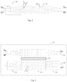
- Figure 2 shows a schematic upper view of a preferred embodiment of the waveguide (100) of the invention (meaning, a view on a plane parallel to the interface between the support (130) and the core (110), and in which the light therefore propagates following the horizontal direction of the figure).
- the waveguide (100) has an effective index (n TE ) for the zero-order transverse electric mode (TE 0 ) and a second effective index (n TM ) for the zero-order transverse magnetic mode (TM 0 ) for each wavelength (A).
- the first effective index (n TE ) can be equal to the second effective index (n TM ), or significantly different from said second effective index (n TM ).
- said waveguide (100) can comprise a modal adapter (140) on each end.
- Each modal adapter (140) has at least one SWG structure with the same period ( ⁇ ) and duty cycle (f) as the waveguide (100), while the width thereof progressively varies from the width of a single mode waveguide to a final width of a modal adapter (140), preferably greater than the width of the single mode waveguide, and thus, preferably, the SWG structures of the modal adapter (140) have an incremental width.
- Each modal adapter (140) likewise comprises a central bridge (141), which is a small connector made of core material in the center of the sections of covering material (120).
- the width of the central bridge reduces as the total width of the respective modal adapter (140) increases, completely disappearing in the interface with the rotated SWG structure. Note that the specific geometry of the modal adapter (140) can vary between implementations, as long as a progressive and smooth modal transition is guaranteed.
- Figure 3 shows a specific embodiment of a polarisation splitter (200) corresponding to a second aspect of the invention and comprises a directional coupler which, in turn, comprises, preferably adjacently arranged, a first single mode guide (210) and a second single mode guide (220), said second single mode guide (220) being a specific embodiment of the waveguide (100) of the first aspect of the invention.
- the first single mode guide (210) is a SWG waveguide with interfaces perpendicular to the axis of the guided light, with modal adapters (140) located on the ends thereof, although in other embodiments of the invention, the first single mode guide (210) can be a continuous waveguide or comprise SWG structures with other alternative geometries.
- the polarisation splitter (200) can comprise a central structure (230) arranged between the first single mode guide (210) and the second single mode guide (220), which allows the polarisation-selective properties of the system to be enhanced and the features thereof to be improved.
- the central structure (230) is simply a rectangular segment, preferably homogeneous of the same material as the sections of core material (110).
- the central structure (230) can be implemented by means of other alternative geometries and/or materials.
- the TE 0 and TM 0 modes are introduced in the same input of the first single mode waveguide (210). While the TM 0 mode couples to the second single mode waveguide (220), following the general behaviour of any directional coupler, the TE 0 mode is confined to the first single mode guide (210), thereby obtaining a highly efficient polarisation split in an extremely reduced size.
- the manufacturing process of the polarisation splitting system (200) is preferably carried out by means of a photonic simulation process consisting of two steps.
- a first step a first approximation of the design is obtained by a simulation of the SWG structure as a homogeneous and anisotropic material.
- the anisotropic material used is defined by a dielectric tensor, obtained by means of Rytov approximation.
- photonic simulations are carried out for a sweep of rotation angles ( ⁇ ), modeling the effect of said rotation by means of the expressions described for the waveguide (100). This first approximation allows simulations to be carried out in three dimensions reducing the computational time and cost of the simulation.
- said modeling is applied to a first optimisation by means of a sweep of different parameters, such as the width of the multimodal zone, the duty cycle of the corresponding real SWG structure or the length of the polarisation splitter.
- Said first optimisation process is done by executing sweeps of the aforementioned parameters and imposing as objectives the minimization of total insertion losses.
- the physical modeling of the complete SWG structure (without approximations to the homogeneous medium) is then carried out, which provides us with the final design of the polarisation splitter (200).
- this process can be done maintaining the degrees of freedom of all the design parameters, it is recommended that this second optimisation process be simplified in order to reduce the computational load of the same, establishing the width of the multimodal zone, the duty cycle, and the period (always imposing that said period be outside the Bragg regime, determined by the proportionality ratio between the period of the SWG structure and the effective wavelength of the light propagated by said structure).
- This second optimisation process is preferably done using three-dimensional finite difference time domain methods (FDTD), although other photonic computational techniques may likewise be applied to the same.
- FDTD three-dimensional finite difference time domain methods
- Figure 4 shows a variant of the polarisation splitter (200) of the invention, wherein the waveguide (100) with which the second waveguide (220) is implemented comprises a plurality of central attachments (140) that connect the sections of core material (110) of the SWG structure.
- the plurality of central attachments (140), and specifically the selection of the width thereof provides an additional degree of freedom in the design of the polarisation splitter (200), increasing the tuning of the first effective index (n TE ) for the zero-order transverse electric mode (TE 0 ) and of the second effective index (n TM ) for the zero-order transverse magnetic mode (TM 0 ).
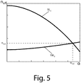
- figure 5 schematically shows a variation of the first effective index (n TE ) for the zero-order transverse electric mode (TE 0 ) and a second effective index (n TM ) for the zero-order transverse magnetic mode (TM 0 ) based on the rotation angle ( ⁇ ) of the SWG structure.
- n TE first effective index
- n TM second effective index
- ⁇ rotation angle
Landscapes
- Physics & Mathematics (AREA)
- General Physics & Mathematics (AREA)
- Optics & Photonics (AREA)
- Chemical & Material Sciences (AREA)
- Dispersion Chemistry (AREA)
- Engineering & Computer Science (AREA)
- Microelectronics & Electronic Packaging (AREA)
- Optical Integrated Circuits (AREA)
Abstract
Description
- The present invention relates to the field of integrated optics, and more specifically, to devices based on waveguides with sub-wavelength structures.
- The birefringence of photonic platforms, meaning the difference in behaviour between transverse electric polarisation (TE) and transverse magnetic polarisation (TM) in devices based on waveguides, is one of the biggest challenges for the development and expansion of integrated optics. In particular there are two main ways to approach this problem: making structures that are polarisation-independent (meaning with the same effective index and/or dispersive characteristics for TE and for TM) or developing polarisation-splitting devices (meaning devices that separate the TE and TM modes into two output guides, independently processing them afterwards, or discarding one of them).
- Regardless of the alternative followed (polarisation-independent or polarisation-selective), the difficulty arises when manipulating the birefringence of the waveguides used, either to match the response of the TE and TM modes or to make it so unequal so as to allow for the separation thereof. In general, given the design constraints obtainable by means of the geometric modification of a single material and etch depth, most solutions in the state of the art are based on the incorporation of additional materials to the core material of the waveguide, or on the use of structures with multiple layers or etch depths. However, these alternatives significantly increase the manufacturing complexity of the devices.
- For example,
US 5,090,790 presents a first polarisation-independent waveguide wherein multiple quantum well layers are introduced in the guide to control the birefringence of the same. In a second example,US 2003/174982 A1 presents an alternative polarisation-independent waveguide wherein an electro-optical coating is deposited, controlled by a set of electrodes that generate a modified magnetic field around the core of the guide, the active control of which allows the effective indices of the TE and TM modes to be matched. As can be seen, in both cases it is necessary to use complex manufacturing and control processes, requiring materials and geometries that are not able to be used with single-exposure manufacturing systems. - With regard to polarisation splitters, different phenomena, materials and optical structures have been proposed with the aim of implementing said polarisation splitters. Noteworthy among the alternatives proposed are sub-wavelength diffraction gratings, photonic crystals, the negative refraction present in said crystals or form birefringence (intrinsic of the materials). However, all of these configurations have serious problems in the manufacturing thereof, either due to a heightened sensitivity to deviations with respect to nominal designs, which are inevitable during the manufacturing process, or due to the fact that they require geometries or auxiliary elements that cannot be implemented by the normal manufacturing methods of commercial photonic chips.
- One possible solution to the previously mentioned manufacturing limitations is the use of multimode interference (MMI) couplers. For example,
US 5,838,842 has an MMI for polarisation splitting in integrated devices. The MMI has a multimode waveguide region (also known as a "slab") in which self-imaging of the transverse electric (TE) and transverse magnetic (TM) modes is generated at different lengths. Said lengths are determined by the differences in the propagation constants of both modes in the multimode waveguide region. However, given that the multimode waveguide region is a continuous waveguide, the differences between the propagation constants are small and hard to control, resulting in devices that are hardly efficient and require large propagation distances in the multimode waveguide region, thereby leading to an increased total size of the device. - It must be noted that multimode interference (MMI) couplers have also been used conventionally for power splitting, in other words, instead of separating two polarisations into two output waveguides, part of the power of a single polarisation is separated into two or more output waveguides. The features of MMI as power splitters, and particularly the losses and the bandwidth thereof, have been improved by means of the use of sub-wavelength grating (SWG) structures, as shown in patent
ES 2,379,058 - Another possible alternative are directional couplers, in which a lateral coupling is produced between two adjacent single mode guides. However, for this coupling to be polarisation-selective, and not merely power splitting (in other words, so that it only affects the TE or TM mode, while the other mode continues to propagate without alterations in the waveguide through which it has been introduced), it is still necessary to control the birefringence of at least one of the single mode guides of which it is made up. Said control can be done by depositing additional materials and/or active elements, with the previously mentioned drawbacks that said option entails, or, as exemplified in
CN 106,959,485 A , by means of the use of SWG structures. - In the case of
CN 106,959,485 A , the SWG structure is etched in a side of one of the single mode guides by means of slits perpendicular to the direction of propagation of light that only partially occupy the core of said guide. However, this geometry provides very limited control of the birefringence of the guide, given that the effects on the TE and TM modes of the structure continue to be linked to each other. This limitation, when independently implementing the effective indices of the TE and TM modes, leads to reduced features with regard to insertion losses, extinction ratio and bandwidth. Additionally, the response of this structure can only be adjusted by modifying the period and duty cycle thereof, which can affect the minimum feature size of the device and therefore does not affect the manufacturing difficulty thereof. - Thus, in the state of the art there is still a need for waveguide structures that are able to provide an efficient and compact polarisation control with a large bandwidth, and without increasing the manufacturing complexity of the devices.
- The present invention solves the previously mentioned problems by means of a single mode waveguide with a SWG structure that is rotated a rotation angle with respect to the propagation direction of the guided light, which allows the birefringence properties of said guide to be modified. The single mode guide herein described can be integrated together with any other combination of devices in a photonic chip, able to be manufactured in the same exposure step as the rest of said devices (unlike other polarisation-independent guides or polarisation splitters that require multiple etch depths, inclined walls, additional materials, etc.).
- In a first aspect of the invention, a modified birefringence guide device is presented, "modified birefringence" being understood not as a real time control of the birefringence of the wave guide, but as a constant alteration of said birefringence with respect to that of a traditional continuous waveguide, said alteration being controllable during a previous guide design phase by means of the selection of the geometric properties of the same, and in particular, of an angle of a SWG structure. The modified birefringence guide device makes use of a modified birefringence waveguide, therefore comprising a SWG structure formed by alternate arrangement of a plurality of sections of a core material and a plurality of sections of a covering material, with a smaller period than the wavelength of the light guided by said modified birefringence waveguide. In particular, the SWG structure is rotated an angle greater than zero with respect to the propagation direction of the light. In other words, the interfaces between the sections of covering material and the sections of core material have said angle with a plane that is perpendicular to the axis of the light propagation. Said angle allows a first effective index for the zero-order transverse electric mode and a second effective index for the zero-order transverse magnetic mode to be independently controlled.
- It must be noted that although other SWG geometric parameters, such as the period or the filling factor can affect the resulting birefringence or anisotropy, said effect is significantly less than that which is produced by the rotation of the interfaces, thereby limiting the features able to be obtained by the splitter. Moreover, it is significant that, unlike said parameters (period and filling factor), the rotation angle does not affect the minimum feature size of the device, and therefore it does not increase the manufacturing difficulty thereof.
- It is likewise noteworthy that the specific angle for which a specific characteristic related to the birefringence is obtained (for example, a specific condition between the first effective index for the zero-order transverse electric mode and the second effective index for the zero-order transverse magnetic mode) depends on the rest of material and morphological characteristics of the guide, such as the height, width, core material, covering material, SWG period and SWG filling factor thereof. Thus, said specific angle is preferably determined in a previous design phase according to the method of the third aspect of the present invention.
- Preferably, said specific conditions obtained by means of the selection of the rotation angle of the SWG structure can comprise both polarisation-independent behaviour (meaning one same value for the first effective index of the zero-order transverse electric mode and for the second effective index of the zero-order transverse magnetic mode) and polarisation-selective behaviour (meaning a value that is significantly different for the first effective index of the zero-order transverse electric mode and for the second effective index of the zero-order transverse magnetic mode.
- Also preferably, depending on the specific embodiment, the geometric parameters (width, period, filling factor, angle) of the SWG structure of the modified birefringence waveguide can either remain constant throughout the whole guide, or be modified in a gradual or abrupt way throughout said guide, thereby obtaining different birefringent properties in different positions of the guide.
- The geometry of the sections of core material can also vary among implementations. In particular, three preferred options include:
- A segment for each section, entirely separated from each other by the covering material. Preferably, each segment has a mainly rectangular or trapezoidal shape (seen on a plane parallel to an interface between a layer of core material and a layer of support material).
- Multiple segments for each section, each pair of segments of one same section being separated by a slit or channel of covering material.
- Sections connected to each other by means of a plurality of central attachments of core material, of either constant or variable width.
- The modified birefringence waveguide is preferably implemented in silicon on insulator (SOI) with a covering material preferably selected among air (meaning, a covering layer is not included during the manufacturing and the air of the environment where the waveguide is applied acts as a covering material), silicon dioxide and a polymer. More preferably, in the case of using a polymer as a covering material, said polymer is selected such that it has an effective index variation with the temperature with a sign opposite to the silicon variation. In other words, by applying a temperature change, the modification in the effective indices of the SWG structure caused by the covering and the core have opposite signs, thereby mitigating the response variability of the guide with respect to environmental changes.
- With the aim of optimising the insertion losses in input and output transitions of the modified birefringence single mode guide (for example, in an interface with a conventional continuous waveguide, or with a SWG guide without rotation), said modified birefringence waveguides preferably comprise at least one modal adapter. The modal adapters comprise SWG structures with a variable width and/or a progressive rotation between a direction perpendicular to the waveguide and the rotation angle of the SWG structure. Also preferably, the modal adapters comprise a central bridge with a width that is inversely proportional to the width of the adapter. For example, if a continuous waveguide with a first width is connected by means of the modal adapter to a modified birefringence waveguide with a second width, said modal adapter progressively increases the width thereof from said first width to said second width, while the central bridge progressively reduces from said first width to a third width (less than the first width), or until completely disappearing at the end of the modal adapter.
- In a second aspect of the invention, a polarisation splitter system is presented which is based on a polarisation-selective directional coupling, made up from the modified birefringence single mode waveguide of the first aspect of the invention. The device comprises two adjacent single mode guides (which we will call first guide and second guide), such that when a zero-order transverse magnetic mode is introduced through the first guide, a coupling to the second guide is produced; while when a zero-order transverse electric mode is introduced through the first guide, said coupling to the second guide is not produced.
- To achieve said polarisation-selective behaviour, at least the second single mode guide comprises a SWG structure, the interfaces of which between the plurality of core material sections and the plurality of covering material sections form an angle greater than zero with a plane that is perpendicular to a propagation direction of guided light. Depending on the specific implementation, the first single mode guide can be a continuous waveguide, a SWG waveguide with interfaces perpendicular to the propagation direction, or a rotated SWG waveguide with geometric properties (width, rotation angle, period and/or filling factor) that are different from those of the second waveguide.
- Preferably, the polarisation-selective behaviour can be enhanced even by means of an auxiliary central structure arranged between the first single mode wave guide and the second single mode wave guide. Specifically, said auxiliary structure can be a homogeneous segment of core material, a homogeneous segment of a material different from the core material, or a heterogeneous structure that combines multiple materials (for example a metamaterial or a SWG structure).
- The control of birefringence provided by the waveguide of the first aspect of the invention, by being applied in the polarisation-splitting system by the directional coupling described, allows the dimensions of the system to be reduced, at the same time that the rest of the features (insertion losses, extinction ration, bandwidth, etc.) are optimised.
- In a third aspect of the invention, a manufacturing method of the modified birefringence waveguide of the first aspect of the invention and, thus, of the polarisation splitter system of the second aspect of the invention, is presented. Given the geometric parameters and/or materials of the SWG structure (for example, width, height, duty cycle, period, covering material, core material), the method comprises determining a rotation angle of the SWG structure to obtain the objective ratio between the first effective index for the zero-order transverse electric mode and a second effective index for the zero-order transverse magnetic mode. Said objective ratio can be, for example, obtaining one same value for the first effective index and the second effective index (polarisation-independent guides), or obtaining a difference greater than a specific threshold between the value of the first effective index and the value of the second effective index (polarisation-selective guides). It must be noted that the geometric and/or material parameters of the SWG structures can be fixed parameters or be iteratively modified within an optimisation process. It must likewise be noted that both the polarisation-independent behaviour and the polarisation-selective behaviour can be obtained for the same geometric and/or material parameters of the SWG structure, simply by modifying the rotation angle of the SWG structure. However, the particular values of the angle for said purposes will depend on the specific values of said geometric and/or material parameters of the SWG structure.
- The calculation of the angle to introduce in the manufactured SWG structure is done by means of numerical computations of the effective indices generated by the SWG structure rotated for said angle. Specifically, said numerical computations can be performed by means of an algorithm selected from among the photonic simulation algorithms known in the state of the art, although preferably, an approximation of the SWG structure is recommended by means of a rotation of a diagonal tensor of homogeneous anisotropic medium, thereby reducing the computational load of the method.
- In particular, the method preferably comprises characterising the SWG structure rotated by means of a rotated tensor (ñ) according to the following expression:


- [nxx, nyy, nzz] being components of the diagonal tensor (n) of a homogeneous anisotropic medium (meaning, the SWG structure without rotating).
- The waveguide, polarisation splitter and design method described therefore provide a compact birefringence control, with low losses and high bandwidth, able to be manufactured in a single lithography step. In other words, the improvement of the features is not associated with an increase in manufacturing complexity. These and other advantages of the invention will become apparent in the light of the detailed description of the same.
- With the aim of helping improve the comprehension of the features of the invention according to a preferred practical embodiment thereof, and to complement this description, the following figures are attached as an integral part of the same, with an illustrative and non-limiting character:
-
Figure 1 schematically shows, in a perspective view, birefringence waveguides modified by means of the rotation of sub-wavelength grating structures according to a preferred embodiment of the invention, illustrating the main geometric parameters of said structure. -
Figure 2 illustrates, in an upper view, a preferred embodiment of the modified birefringence waveguide of the invention, wherein the rotation angle is selected such that a polarisation-independent behaviour is obtained. -
Figure 3 shows an integrated polarisation splitter based on directional coupling with a modified birefringence waveguide, according to a preferred embodiment of the invention. -
Figure 4 illustrates the effect of the rotation angle on the anisotropic properties of a SWG structure. -
Figure 5 illustrates a chart showing the variation of the first effective index (nTE) for the zero-order transverse electric mode (TE0) and a second effective index (nTM) for the zero-order transverse magnetic mode (TM0) based on the rotation angle (α) of the SWG structure. - Note that the preferred embodiments of the device (modified birefringence single mode waveguide) and of the associated system thereof (polarisation splitter based on said guide) object of the invention is preferably implemented in silicon on insulator (SOI) to thus benefit from the high contrast of the SOI index. However, specific embodiments could be implemented in other different photonic platforms. In other words, all of the waveguides of the device are preferably made by means of a silicon core, deposited on an insulating layer, such as silicon dioxide. The covering material can vary for different embodiments of the invention, some of the possibilities being silicon dioxide, polymers or air, without this list limiting the use of other possible options.
- Likewise, it must be noted that the preferred embodiments of the polarisation splitter of the invention are described with the system operating as a polarisation splitter. However, the same system can operate in a reciprocal manner as a polarisation multiplexer, in other words, combining two orthogonal polarisation signals of two input guides in a single output guide, simply by reversing the operating direction of the device.
- With regard to the manufacturing of the devices proposed, it must be noted that the sub-wavelength grating (SWG) structures, independent of the rotation angle thereof with respect to the optical axis, do not increase the difficulty or the number of steps with respect to the manufacturing of conventional waveguides. In other words, all of the structures used by the polarisation splitter of the invention can be manufactured in a single exposure step at a complete depth with any conventional microelectronic etching technique, for example by means of exposure to e-beams or deep-UV.
-
Figure 1 shows a schematic view of a preferred embodiment of a waveguide (100), preferably single mode, which allows the birefringence of the light that passes through at least part of said waveguide (100) object of a first aspect of the invention to be modified, likewise used in a preferred embodiment of the polarisation splitter (200) object of a second aspect of the invention, as well as the main geometric parameters thereof. - The waveguide (100) is formed by a periodic alternative arrangement of sections of a core material (110) and sections of a covering material (120) with a period (Λ) smaller than the wavelength of a light propagated by said periodic arrangement of the waveguide (100); further having, arranged between the sections of core material (110) and sections of a covering material (120), interfaces that are rotated an angle (α) with respect to a plane perpendicular to the propagation direction of the light (meaning, perpendicular to the main axis of the waveguide). The core material sections (110) of the wave guide (100) have a height (H) and a width (W) and are arranged on a support material (130) which acts as an insulating layer. On this structure, a filling factor or duty cycle (f) is defined as the ratio between the proportion of covering material (a) and the proportion of core material (b) within a period (Λ). The specific values of all of these geometric parameters are defined prior to the manufacturing of the device by means of numeric simulations according to that described by the method of the invention.
- Specifically, the waveguide (100) is preferably modeled as a rotated tensor (ñ) according to the following expression:


- [nxx, nyy, nzz] being components of a diagonal tensor (n) of the homogeneous anisotropic medium equivalent to the SWG structure without rotating (meaning, with interfaces perpendicular to the main axis of the waveguide). This modeling can provide a final value of the angle (α), or serve as a first approximation, refined in a second calculation step by means of a complete simulation (meaning, without approximations of SWG structures as homogeneous means) of the structure.
-
Figure 2 shows a schematic upper view of a preferred embodiment of the waveguide (100) of the invention (meaning, a view on a plane parallel to the interface between the support (130) and the core (110), and in which the light therefore propagates following the horizontal direction of the figure). The waveguide (100) has an effective index (nTE) for the zero-order transverse electric mode (TE0) and a second effective index (nTM) for the zero-order transverse magnetic mode (TM0) for each wavelength (A). Depending on the angle (α), for specific geometric and material conditions, the first effective index (nTE) can be equal to the second effective index (nTM), or significantly different from said second effective index (nTM). The necessary difference in order for it to be considered a "significantly different" value depends on the specific application of the device, but in general, this expression must be understood as a difference of propagation characteristics that allows for differential processing of the TE0 y TM0 modes. For example, in the case of using the waveguide (100) for implementing a polarisation splitter (200), "significantly different" is understood as an effective index difference that gives rise to the lateral coupling of the TM0 mode between adjacent guides, while said coupling does not occur in the TE0 mode (due to a greater first effective index of said TE0 mode with respect to the second effective index of the TM0 mode and, thus, a smaller modal diameter). - With the aim of reducing the reflection losses in the interfaces of the waveguide (100), said waveguide (100) can comprise a modal adapter (140) on each end. Each modal adapter (140) has at least one SWG structure with the same period (Λ) and duty cycle (f) as the waveguide (100), while the width thereof progressively varies from the width of a single mode waveguide to a final width of a modal adapter (140), preferably greater than the width of the single mode waveguide, and thus, preferably, the SWG structures of the modal adapter (140) have an incremental width. Each modal adapter (140) likewise comprises a central bridge (141), which is a small connector made of core material in the center of the sections of covering material (120). The width of the central bridge reduces as the total width of the respective modal adapter (140) increases, completely disappearing in the interface with the rotated SWG structure. Note that the specific geometry of the modal adapter (140) can vary between implementations, as long as a progressive and smooth modal transition is guaranteed.
-
Figure 3 shows a specific embodiment of a polarisation splitter (200) corresponding to a second aspect of the invention and comprises a directional coupler which, in turn, comprises, preferably adjacently arranged, a first single mode guide (210) and a second single mode guide (220), said second single mode guide (220) being a specific embodiment of the waveguide (100) of the first aspect of the invention. In this case, the first single mode guide (210) is a SWG waveguide with interfaces perpendicular to the axis of the guided light, with modal adapters (140) located on the ends thereof, although in other embodiments of the invention, the first single mode guide (210) can be a continuous waveguide or comprise SWG structures with other alternative geometries. - Additionally, the polarisation splitter (200) can comprise a central structure (230) arranged between the first single mode guide (210) and the second single mode guide (220), which allows the polarisation-selective properties of the system to be enhanced and the features thereof to be improved. In this example, the central structure (230) is simply a rectangular segment, preferably homogeneous of the same material as the sections of core material (110). However, in other specific embodiments, the central structure (230) can be implemented by means of other alternative geometries and/or materials.
- During the operation as a polarisation splitter (200), the TE0 and TM0 modes are introduced in the same input of the first single mode waveguide (210). While the TM0 mode couples to the second single mode waveguide (220), following the general behaviour of any directional coupler, the TE0 mode is confined to the first single mode guide (210), thereby obtaining a highly efficient polarisation split in an extremely reduced size.
- The manufacturing process of the polarisation splitting system (200) is preferably carried out by means of a photonic simulation process consisting of two steps. In a first step, a first approximation of the design is obtained by a simulation of the SWG structure as a homogeneous and anisotropic material. The anisotropic material used is defined by a dielectric tensor, obtained by means of Rytov approximation. Establishing these starting parameters, photonic simulations are carried out for a sweep of rotation angles (α), modeling the effect of said rotation by means of the expressions described for the waveguide (100). This first approximation allows simulations to be carried out in three dimensions reducing the computational time and cost of the simulation.
- Once the anisotropic properties are modeled at different angles for the specific geometry and platform under analysis, said modeling is applied to a first optimisation by means of a sweep of different parameters, such as the width of the multimodal zone, the duty cycle of the corresponding real SWG structure or the length of the polarisation splitter. Said first optimisation process is done by executing sweeps of the aforementioned parameters and imposing as objectives the minimization of total insertion losses. As a result of this optimisation, an approximation of the initial design parameters (angle, separation between guides, period, duty cycle and length of the device) is obtained.
- From the design parameters obtained in the first step, the physical modeling of the complete SWG structure (without approximations to the homogeneous medium) is then carried out, which provides us with the final design of the polarisation splitter (200). Although this process can be done maintaining the degrees of freedom of all the design parameters, it is recommended that this second optimisation process be simplified in order to reduce the computational load of the same, establishing the width of the multimodal zone, the duty cycle, and the period (always imposing that said period be outside the Bragg regime, determined by the proportionality ratio between the period of the SWG structure and the effective wavelength of the light propagated by said structure). This second optimisation process is preferably done using three-dimensional finite difference time domain methods (FDTD), although other photonic computational techniques may likewise be applied to the same.
-
Figure 4 shows a variant of the polarisation splitter (200) of the invention, wherein the waveguide (100) with which the second waveguide (220) is implemented comprises a plurality of central attachments (140) that connect the sections of core material (110) of the SWG structure. The plurality of central attachments (140), and specifically the selection of the width thereof provides an additional degree of freedom in the design of the polarisation splitter (200), increasing the tuning of the first effective index (nTE) for the zero-order transverse electric mode (TE0) and of the second effective index (nTM) for the zero-order transverse magnetic mode (TM0). - Lastly,
figure 5 schematically shows a variation of the first effective index (nTE) for the zero-order transverse electric mode (TE0) and a second effective index (nTM) for the zero-order transverse magnetic mode (TM0) based on the rotation angle (α) of the SWG structure. In spite of the fact that the specific dependencies of these indices with the angle (α) vary based on the materials used and the rest of the geometric properties, it must be mentioned that the effect of said rotation is greater for the TE0 mode than for the TM0 mode, and furthermore the variation thereof have opposite signs. This allows, on the one hand, the properties of the first effective index (nTE) to be altered without hardly modifying the response of the second effective index (nTM), thereby developing polarisation-selective devices; and on the other hand, determining an angle for polarisation independence (αind) in which it is verified that both the first effective index (nTE) and the second effective index (nTM) are equal to each other, taking a value of the polarisation-independent effective index (nind). - In light of this description and figures, a person skilled in the art will be able to understand that the invention has been described according to some preferred embodiments of the same, but multiple variations may be introduced in said preferred embodiments, without detracting from the object of the invention as claimed.
Claims (25)
- A waveguide (100) comprising a plurality of sections of a core material (110) and a plurality of sections of a covering material (120) alternately arranged in a periodic way with a period (Λ) smaller than the wavelength (A) of a light guided through the waveguide (100);
the waveguide (100) characterised in that it is single mode and comprises interfaces respectively defined between each one of the sections of the plurality of sections of core material (110) and each one of the sections of the plurality of sections of covering material (120) forming an angle (α) greater than zero with respect to a plane perpendicular to a propagation direction of the light intended to be guided by the waveguide (100). - The waveguide (100) according to claim 1, characterised in that the angle (α) is selected such that a first effective index (nTE) of a zero-order transverse electric mode (TE0) is different from a second effective index (nTM) of a zero-order transverse magnetic mode (TM0).
- The waveguide (100) according to claim 1, characterised in that the angle (α) is selected such that a first effective index (nTE) of a zero-order transverse electric mode (TE0) is equal to a second effective index (nTM) of a zero-order transverse magnetic mode (TM0).
- The waveguide (100) according to any of the preceding claims, characterised in that it comprises at least one modal adapter (140) connected to an input of the waveguide (100), said at least one modal adapter (140) comprising a plurality of sections of core material (110) and sections of covering material (120) arranged in an alternated and periodic way with a period (Λ) smaller than the wavelength (A) of a light guided through the at least one modal adapter (140), and the plurality of sections of core material (110) being arranged with progressive angles between a plane perpendicular to the propagation direction of the guided light and the angle (α).
- The waveguide (100) according to claim 4, characterised in that the at least one modal adapter (140) comprises a plurality of central attachments (141) of core material that joins the plurality of sections of core material (110) of said modal adapter (140), the width of each central bridge (141) being inversely proportional to the width of the modal adapter (140).
- The waveguide (100) according to any one of claims 4 and 5, characterised in that the sections of core material (210) of the at least one modal adapter (140) have a variable width.
- The waveguide (100) according to any one of the preceding claims, characterised in that the plurality of sections of core material (110) and the plurality of sections of covering material (120) have constant geometric properties throughout the length of the waveguide (100).
- The waveguide (100) according to any one of claims 1 to 6, characterised in that the plurality of sections of core material (110) and the plurality of sections of covering material (120) have variable geometric properties throughout the length of the waveguide (100).
- The waveguide (100) according to any one of the preceding claims, characterised in that the plurality of sections of core material (110) have at least one inner groove of covering material.
- The waveguide (100) according to any one of claims 1 to 8, characterised in that the plurality of sections of core material (110) have a plurality of central attachments (150) of core material.
- The waveguide (100) according to any one of the preceding claims, characterised in that the material of the sections of core material (110) is silicon.
- The waveguide (100) according to claim 11, characterised in that the material of the sections of covering material (120) is silicon dioxide.
- The waveguide (100) according to claim 11, characterised in that the material of the sections of covering material (120) is a polymer with an effective index variation with the temperature value having the sign opposite to the variation of the silicon of the sections of core material (110).
- The waveguide (100) according to claim 13, characterised in that the proportion of covering material with respect to the material of the sections of core material (110) within a period (Λ) is selected such that a variation is minimised with the temperature of the first effective index (nTE) and the second effective index (nTM).
- A polarisation splitter (200), comprising a first waveguide (210) and a second waveguide (220) adjacently arranged at a distance (d), characterised in that at least the second waveguide (220) is a waveguide (100) according to any one of claims 1 to 14.
- The polarisation splitter (200) according to claim 15, characterised in that the first waveguide (210) is a continuous waveguide.
- The polarisation splitter (200) according to claim 15, characterised in that the first waveguide (210) is a waveguide with a plurality of sections of a core material (110) and a plurality of sections of a covering material (120) alternately arranged in a periodic way with a period (Λ) smaller than the wavelength (A) of the guided light.
- The polarisation splitter (200) according to any one of claims 15 to 17, characterised in that it further comprises a central structure (230) arranged between the first waveguide (210) and the second waveguide (220).
- The polarisation splitter (200) according to claim 18, characterised in that the central structure (230) is a homogeneous segment of core material.
- The polarisation splitter (200) according to claim 18, characterised in that the central structure (230) is a homogeneous segment of a material different than the core material.
- The polarisation splitter (200) according to claim 18, characterised in that the central structure (230) is a heterogeneous structure that combines multiple materials.
- A manufacturing method of the waveguide (100) described in any one of claims 1 to 14, characterised in that it comprises, given a core material and a covering material of the waveguide (100), arranging a plurality of sections of core material (110) and a plurality of sections of covering material (120), defining between each one of the sections of core material (110) and each one of the sections of covering material (120) interfaces that respectively form an angle (α) greater than zero with respect to a plane perpendicular to a propagation direction of the light intended to be guided by the waveguide (100).
- The method according to claim 22, characterised in that the angle (α) is determined by means of the approximation of the waveguide (100) making use of a rotated tensor (ñ), resulting from rotating a diagonal tensor (n) of a homogeneous anisotropic medium.
- The method according to claim 23, characterised in that it comprises calculating the rotated tensor (ñ) according to:



- [nxx, nyy, nzz] being components of the diagonal tensor (n) of the homogeneous anisotropic medium.
Applications Claiming Priority (2)
| Application Number | Priority Date | Filing Date | Title |
|---|---|---|---|
| ES201830653A ES2736899B2 (en) | 2018-06-29 | 2018-06-29 | WAVE GUIDE, METHOD OF MANUFACTURE OF SUCH WAVE GUIDE AND POLARIZATION DIVIDER THAT MAKES USE OF SUCH WAVE GUIDE |
| PCT/ES2019/070452 WO2020002739A1 (en) | 2018-06-29 | 2019-06-27 | Waveguide, waveguide production method, and polarisation splitter using said waveguide |
Publications (2)
| Publication Number | Publication Date |
|---|---|
| EP3816687A1 true EP3816687A1 (en) | 2021-05-05 |
| EP3816687B1 EP3816687B1 (en) | 2025-05-14 |
Family
ID=67777349
Family Applications (1)
| Application Number | Title | Priority Date | Filing Date |
|---|---|---|---|
| EP19759632.3A Active EP3816687B1 (en) | 2018-06-29 | 2019-06-27 | Waveguide, waveguide production method, and polarisation splitter using said waveguide |
Country Status (5)
| Country | Link |
|---|---|
| US (2) | US11644612B2 (en) |
| EP (1) | EP3816687B1 (en) |
| ES (2) | ES2736899B2 (en) |
| SG (1) | SG11202013094UA (en) |
| WO (1) | WO2020002739A1 (en) |
Families Citing this family (3)
| Publication number | Priority date | Publication date | Assignee | Title |
|---|---|---|---|---|
| ES2872650B2 (en) * | 2020-04-29 | 2022-03-11 | Univ Malaga | BRICKED SUB-WAVELENGTH PERIODIC WAVEGUIDE, MODAL ADAPTER, POWER SPLITTER AND POLARIZATION SPLITTER MAKE USE OF SUCH WAVEGUIDE |
| CN112051641B (en) * | 2020-10-12 | 2024-12-03 | 苏州科沃微电子有限公司 | Tilted grating type polarization beam splitter using slit waveguide structure and manufacturing method thereof |
| ES2981814A1 (en) * | 2023-03-10 | 2024-10-10 | Consejo Superior Investigacion | POWER DIVIDER DEVICE INTEGRATED IN WAVEGUIDES (Machine-translation by Google Translate, not legally binding) |
Family Cites Families (8)
| Publication number | Priority date | Publication date | Assignee | Title |
|---|---|---|---|---|
| US5090790A (en) | 1990-06-29 | 1992-02-25 | At&T Bell Laboratories | Polarization-independent semiconductor waveguide |
| JP3142081B2 (en) * | 1992-04-13 | 2001-03-07 | 日本電信電話株式会社 | Waveguide type optical branching device |
| US5838842A (en) | 1997-01-10 | 1998-11-17 | The United States Of America As Represented By The Secretary Of The Army | Self-imaging waveguide optical polarization or wavelength splitters |
| US6795597B2 (en) | 2002-03-15 | 2004-09-21 | Optimer Photonics, Inc. | Electrode and core arrangements for polarization-independent waveguides |
| ES2379058B2 (en) | 2012-02-23 | 2012-10-01 | Universidad De Málaga | Waveguide coupler device, and design method of said device |
| US9411106B2 (en) * | 2014-09-30 | 2016-08-09 | International Business Machines Corporation | Polarization-independent grating coupler for silicon on insulator |
| CN106959485B (en) | 2017-04-28 | 2023-06-06 | 中国人民解放军国防科学技术大学 | Directional coupling TM polarizer and beam splitter based on subwavelength grating |
| ES2722753A1 (en) * | 2018-02-13 | 2019-08-16 | Consejo Superior Investigacion | INTEGRATED POLARIZATION DIVIDER (Machine-translation by Google Translate, not legally binding) |
-
2018
- 2018-06-29 ES ES201830653A patent/ES2736899B2/en active Active
-
2019
- 2019-06-27 EP EP19759632.3A patent/EP3816687B1/en active Active
- 2019-06-27 US US17/255,937 patent/US11644612B2/en active Active
- 2019-06-27 WO PCT/ES2019/070452 patent/WO2020002739A1/en not_active Ceased
- 2019-06-27 ES ES19759632T patent/ES3037085T3/en active Active
- 2019-06-27 SG SG11202013094UA patent/SG11202013094UA/en unknown
-
2023
- 2023-04-07 US US18/297,556 patent/US20230251414A1/en not_active Abandoned
Also Published As
| Publication number | Publication date |
|---|---|
| SG11202013094UA (en) | 2021-01-28 |
| US11644612B2 (en) | 2023-05-09 |
| ES3037085T3 (en) | 2025-09-26 |
| US20230251414A1 (en) | 2023-08-10 |
| ES2736899A1 (en) | 2020-01-08 |
| EP3816687B1 (en) | 2025-05-14 |
| ES2736899B2 (en) | 2020-05-11 |
| WO2020002739A4 (en) | 2020-03-26 |
| WO2020002739A1 (en) | 2020-01-02 |
| US20210263210A1 (en) | 2021-08-26 |
Similar Documents
| Publication | Publication Date | Title |
|---|---|---|
| US11131809B2 (en) | Integrated polarization splitter | |
| US20230251414A1 (en) | Waveguide, waveguide production method, and polarisation splitter using said waveguide | |
| Piggott et al. | Fabrication-constrained nanophotonic inverse design | |
| JP4398275B2 (en) | Light control element | |
| US10031291B1 (en) | Multi-mode interferometer coupler with core strips | |
| US10746932B2 (en) | Multi-mode interference coupler | |
| US20160091664A1 (en) | Polarization-independent grating coupler for silicon on insulator | |
| CN111819480A (en) | Photonic devices for converting light modes of light beams | |
| JP2006276857A (en) | Optical coupler device and method | |
| US20040258361A1 (en) | Low-loss optical waveguide crossovers using an out-of-plane waveguide | |
| KR101023254B1 (en) | Plasmon permeation filter | |
| de Cabo et al. | Extending the spectral operation of multimode and polarization-independent power splitters through subwavelength nanotechnology | |
| Zhang et al. | A Polarization-Insensitive 3dB Power Splitter Based On Inverse-Designed Subwavelength Pixelated Structure | |
| KR20230028245A (en) | Brick-type sub-wavelength periodic waveguides, modal adapters, power dividers, and polarization splitters using the waveguides | |
| Le | Design of a polarization independent MMI SOI coupler based microresonator using sandwich structures | |
| US20030118289A1 (en) | Radiation-free optical cavity | |
| EP4650863A1 (en) | Fabrication tolerant and temperature tolerant mach zehnder interferometers | |
| TW202609257A (en) | Fabrication tolerant and temperature tolerant mach zehnder interferometers | |
| Rabus et al. | Building Blocks of Ring Resonator Devices | |
| Timotijevic et al. | Optical filters in silicon-on-insulator: design considerations for devices based upon strip and rib waveguides | |
| Osgood jr et al. | Passive Waveguide Components | |
| Teng | Design and characterization of optical fiber-to-chip edge couplers and on-chip mode division multiplexing devices | |
| US7680383B1 (en) | Semiconductor-based broadband modulators | |
| Xu et al. | Selecting the polarization in silicon photonic wire components | |
| Ayre | Photonic crystal interfaces: a design-driven approach |
Legal Events
| Date | Code | Title | Description |
|---|---|---|---|
| STAA | Information on the status of an ep patent application or granted ep patent |
Free format text: STATUS: UNKNOWN |
|
| STAA | Information on the status of an ep patent application or granted ep patent |
Free format text: STATUS: THE INTERNATIONAL PUBLICATION HAS BEEN MADE |
|
| PUAI | Public reference made under article 153(3) epc to a published international application that has entered the european phase |
Free format text: ORIGINAL CODE: 0009012 |
|
| STAA | Information on the status of an ep patent application or granted ep patent |
Free format text: STATUS: REQUEST FOR EXAMINATION WAS MADE |
|
| 17P | Request for examination filed |
Effective date: 20210128 |
|
| AK | Designated contracting states |
Kind code of ref document: A1 Designated state(s): AL AT BE BG CH CY CZ DE DK EE ES FI FR GB GR HR HU IE IS IT LI LT LU LV MC MK MT NL NO PL PT RO RS SE SI SK SM TR |
|
| DAV | Request for validation of the european patent (deleted) | ||
| DAX | Request for extension of the european patent (deleted) | ||
| RIN1 | Information on inventor provided before grant (corrected) |
Inventor name: VILLAFRANCA VELASCO, AITOR Inventor name: WANGUEEMERT PEREZ, JUAN GONZALO Inventor name: MOLINA FERNANDEZ, INIGO Inventor name: ORTEGA MONUX, ALEJANDRO Inventor name: HERRERO BERMELLO, ALAINE Inventor name: LUQUE GONZALEZ, JOSE MANUEL Inventor name: HALIR, ROBERT |
|
| STAA | Information on the status of an ep patent application or granted ep patent |
Free format text: STATUS: EXAMINATION IS IN PROGRESS |
|
| 17Q | First examination report despatched |
Effective date: 20221103 |
|
| GRAP | Despatch of communication of intention to grant a patent |
Free format text: ORIGINAL CODE: EPIDOSNIGR1 |
|
| STAA | Information on the status of an ep patent application or granted ep patent |
Free format text: STATUS: GRANT OF PATENT IS INTENDED |
|
| INTG | Intention to grant announced |
Effective date: 20241210 |
|
| GRAS | Grant fee paid |
Free format text: ORIGINAL CODE: EPIDOSNIGR3 |
|
| GRAA | (expected) grant |
Free format text: ORIGINAL CODE: 0009210 |
|
| STAA | Information on the status of an ep patent application or granted ep patent |
Free format text: STATUS: THE PATENT HAS BEEN GRANTED |
|
| AK | Designated contracting states |
Kind code of ref document: B1 Designated state(s): AL AT BE BG CH CY CZ DE DK EE ES FI FR GB GR HR HU IE IS IT LI LT LU LV MC MK MT NL NO PL PT RO RS SE SI SK SM TR |
|
| REG | Reference to a national code |
Ref country code: GB Ref legal event code: FG4D |
|
| REG | Reference to a national code |
Ref country code: CH Ref legal event code: EP |
|
| REG | Reference to a national code |
Ref country code: IE Ref legal event code: FG4D |
|
| REG | Reference to a national code |
Ref country code: DE Ref legal event code: R096 Ref document number: 602019069983 Country of ref document: DE |
|
| P01 | Opt-out of the competence of the unified patent court (upc) registered |
Free format text: CASE NUMBER: APP_24616/2025 Effective date: 20250522 |
|
| PGFP | Annual fee paid to national office [announced via postgrant information from national office to epo] |
Ref country code: NL Payment date: 20250722 Year of fee payment: 7 |
|
| REG | Reference to a national code |
Ref country code: NL Ref legal event code: FP |
|
| REG | Reference to a national code |
Ref country code: ES Ref legal event code: FG2A Ref document number: 3037085 Country of ref document: ES Kind code of ref document: T3 Effective date: 20250926 |
|
| PG25 | Lapsed in a contracting state [announced via postgrant information from national office to epo] |
Ref country code: PT Free format text: LAPSE BECAUSE OF FAILURE TO SUBMIT A TRANSLATION OF THE DESCRIPTION OR TO PAY THE FEE WITHIN THE PRESCRIBED TIME-LIMIT Effective date: 20250915 Ref country code: FI Free format text: LAPSE BECAUSE OF FAILURE TO SUBMIT A TRANSLATION OF THE DESCRIPTION OR TO PAY THE FEE WITHIN THE PRESCRIBED TIME-LIMIT Effective date: 20250514 |
|
| PGFP | Annual fee paid to national office [announced via postgrant information from national office to epo] |
Ref country code: ES Payment date: 20250708 Year of fee payment: 7 |
|
| PGFP | Annual fee paid to national office [announced via postgrant information from national office to epo] |
Ref country code: DE Payment date: 20250722 Year of fee payment: 7 |
|
| REG | Reference to a national code |
Ref country code: LT Ref legal event code: MG9D |
|
| PG25 | Lapsed in a contracting state [announced via postgrant information from national office to epo] |
Ref country code: GR Free format text: LAPSE BECAUSE OF FAILURE TO SUBMIT A TRANSLATION OF THE DESCRIPTION OR TO PAY THE FEE WITHIN THE PRESCRIBED TIME-LIMIT Effective date: 20250815 Ref country code: NO Free format text: LAPSE BECAUSE OF FAILURE TO SUBMIT A TRANSLATION OF THE DESCRIPTION OR TO PAY THE FEE WITHIN THE PRESCRIBED TIME-LIMIT Effective date: 20250814 |
|
| PG25 | Lapsed in a contracting state [announced via postgrant information from national office to epo] |
Ref country code: PL Free format text: LAPSE BECAUSE OF FAILURE TO SUBMIT A TRANSLATION OF THE DESCRIPTION OR TO PAY THE FEE WITHIN THE PRESCRIBED TIME-LIMIT Effective date: 20250514 |
|
| REG | Reference to a national code |
Ref country code: AT Ref legal event code: MK05 Ref document number: 1795249 Country of ref document: AT Kind code of ref document: T Effective date: 20250514 |
|
| PG25 | Lapsed in a contracting state [announced via postgrant information from national office to epo] |
Ref country code: BG Free format text: LAPSE BECAUSE OF FAILURE TO SUBMIT A TRANSLATION OF THE DESCRIPTION OR TO PAY THE FEE WITHIN THE PRESCRIBED TIME-LIMIT Effective date: 20250514 |
|
| PGFP | Annual fee paid to national office [announced via postgrant information from national office to epo] |
Ref country code: BE Payment date: 20250722 Year of fee payment: 7 Ref country code: GB Payment date: 20250721 Year of fee payment: 7 |
|
| PG25 | Lapsed in a contracting state [announced via postgrant information from national office to epo] |
Ref country code: HR Free format text: LAPSE BECAUSE OF FAILURE TO SUBMIT A TRANSLATION OF THE DESCRIPTION OR TO PAY THE FEE WITHIN THE PRESCRIBED TIME-LIMIT Effective date: 20250514 |
|
| PG25 | Lapsed in a contracting state [announced via postgrant information from national office to epo] |
Ref country code: AT Free format text: LAPSE BECAUSE OF FAILURE TO SUBMIT A TRANSLATION OF THE DESCRIPTION OR TO PAY THE FEE WITHIN THE PRESCRIBED TIME-LIMIT Effective date: 20250514 |
|
| PGFP | Annual fee paid to national office [announced via postgrant information from national office to epo] |
Ref country code: FR Payment date: 20250715 Year of fee payment: 7 |
|
| PG25 | Lapsed in a contracting state [announced via postgrant information from national office to epo] |
Ref country code: RS Free format text: LAPSE BECAUSE OF FAILURE TO SUBMIT A TRANSLATION OF THE DESCRIPTION OR TO PAY THE FEE WITHIN THE PRESCRIBED TIME-LIMIT Effective date: 20250814 |
|
| PGFP | Annual fee paid to national office [announced via postgrant information from national office to epo] |
Ref country code: IE Payment date: 20250715 Year of fee payment: 7 |
|
| PG25 | Lapsed in a contracting state [announced via postgrant information from national office to epo] |
Ref country code: IS Free format text: LAPSE BECAUSE OF FAILURE TO SUBMIT A TRANSLATION OF THE DESCRIPTION OR TO PAY THE FEE WITHIN THE PRESCRIBED TIME-LIMIT Effective date: 20250914 |
|
| PG25 | Lapsed in a contracting state [announced via postgrant information from national office to epo] |
Ref country code: LV Free format text: LAPSE BECAUSE OF FAILURE TO SUBMIT A TRANSLATION OF THE DESCRIPTION OR TO PAY THE FEE WITHIN THE PRESCRIBED TIME-LIMIT Effective date: 20250514 |
|
| PG25 | Lapsed in a contracting state [announced via postgrant information from national office to epo] |
Ref country code: DK Free format text: LAPSE BECAUSE OF FAILURE TO SUBMIT A TRANSLATION OF THE DESCRIPTION OR TO PAY THE FEE WITHIN THE PRESCRIBED TIME-LIMIT Effective date: 20250514 Ref country code: SM Free format text: LAPSE BECAUSE OF FAILURE TO SUBMIT A TRANSLATION OF THE DESCRIPTION OR TO PAY THE FEE WITHIN THE PRESCRIBED TIME-LIMIT Effective date: 20250514 |
|
| PG25 | Lapsed in a contracting state [announced via postgrant information from national office to epo] |
Ref country code: CZ Free format text: LAPSE BECAUSE OF FAILURE TO SUBMIT A TRANSLATION OF THE DESCRIPTION OR TO PAY THE FEE WITHIN THE PRESCRIBED TIME-LIMIT Effective date: 20250514 |
|
| PG25 | Lapsed in a contracting state [announced via postgrant information from national office to epo] |
Ref country code: EE Free format text: LAPSE BECAUSE OF FAILURE TO SUBMIT A TRANSLATION OF THE DESCRIPTION OR TO PAY THE FEE WITHIN THE PRESCRIBED TIME-LIMIT Effective date: 20250514 |
|
| PG25 | Lapsed in a contracting state [announced via postgrant information from national office to epo] |
Ref country code: SK Free format text: LAPSE BECAUSE OF FAILURE TO SUBMIT A TRANSLATION OF THE DESCRIPTION OR TO PAY THE FEE WITHIN THE PRESCRIBED TIME-LIMIT Effective date: 20250514 Ref country code: RO Free format text: LAPSE BECAUSE OF FAILURE TO SUBMIT A TRANSLATION OF THE DESCRIPTION OR TO PAY THE FEE WITHIN THE PRESCRIBED TIME-LIMIT Effective date: 20250514 |
|
| REG | Reference to a national code |
Ref country code: CH Ref legal event code: H13 Free format text: ST27 STATUS EVENT CODE: U-0-0-H10-H13 (AS PROVIDED BY THE NATIONAL OFFICE) Effective date: 20260127 |
|
| PG25 | Lapsed in a contracting state [announced via postgrant information from national office to epo] |
Ref country code: IT Free format text: LAPSE BECAUSE OF FAILURE TO SUBMIT A TRANSLATION OF THE DESCRIPTION OR TO PAY THE FEE WITHIN THE PRESCRIBED TIME-LIMIT Effective date: 20250514 |
|
| PG25 | Lapsed in a contracting state [announced via postgrant information from national office to epo] |
Ref country code: LU Free format text: LAPSE BECAUSE OF NON-PAYMENT OF DUE FEES Effective date: 20250627 |
|
| REG | Reference to a national code |
Ref country code: DE Ref legal event code: R097 Ref document number: 602019069983 Country of ref document: DE |
|
| PG25 | Lapsed in a contracting state [announced via postgrant information from national office to epo] |
Ref country code: MC Free format text: LAPSE BECAUSE OF FAILURE TO SUBMIT A TRANSLATION OF THE DESCRIPTION OR TO PAY THE FEE WITHIN THE PRESCRIBED TIME-LIMIT Effective date: 20250514 |
|
| PLBE | No opposition filed within time limit |
Free format text: ORIGINAL CODE: 0009261 |
|
| STAA | Information on the status of an ep patent application or granted ep patent |
Free format text: STATUS: NO OPPOSITION FILED WITHIN TIME LIMIT |
|
| REG | Reference to a national code |
Ref country code: CH Ref legal event code: L10 Free format text: ST27 STATUS EVENT CODE: U-0-0-L10-L00 (AS PROVIDED BY THE NATIONAL OFFICE) Effective date: 20260325 |
|
| 26N | No opposition filed |
Effective date: 20260217 |
|
| PG25 | Lapsed in a contracting state [announced via postgrant information from national office to epo] |
Ref country code: CH Free format text: LAPSE BECAUSE OF NON-PAYMENT OF DUE FEES Effective date: 20250630 |