EP3813246A1 - Full-bridge inverter with unipolar switching scheme and its method of operation - Google Patents
Full-bridge inverter with unipolar switching scheme and its method of operation Download PDFInfo
- Publication number
- EP3813246A1 EP3813246A1 EP19205300.7A EP19205300A EP3813246A1 EP 3813246 A1 EP3813246 A1 EP 3813246A1 EP 19205300 A EP19205300 A EP 19205300A EP 3813246 A1 EP3813246 A1 EP 3813246A1
- Authority
- EP
- European Patent Office
- Prior art keywords
- inductor
- switch
- diode
- full
- bridge inverter
- Prior art date
- Legal status (The legal status is an assumption and is not a legal conclusion. Google has not performed a legal analysis and makes no representation as to the accuracy of the status listed.)
- Granted
Links
Images


Classifications
-
- H—ELECTRICITY
- H02—GENERATION; CONVERSION OR DISTRIBUTION OF ELECTRIC POWER
- H02M—APPARATUS FOR CONVERSION BETWEEN AC AND AC, BETWEEN AC AND DC, OR BETWEEN DC AND DC, AND FOR USE WITH MAINS OR SIMILAR POWER SUPPLY SYSTEMS; CONVERSION OF DC OR AC INPUT POWER INTO SURGE OUTPUT POWER; CONTROL OR REGULATION THEREOF
- H02M7/00—Conversion of AC power input into DC power output; Conversion of DC power input into AC power output
- H02M7/42—Conversion of DC power input into AC power output without possibility of reversal
- H02M7/44—Conversion of DC power input into AC power output without possibility of reversal by static converters
- H02M7/48—Conversion of DC power input into AC power output without possibility of reversal by static converters using discharge tubes with control electrode or semiconductor devices with control electrode
- H02M7/53—Conversion of DC power input into AC power output without possibility of reversal by static converters using discharge tubes with control electrode or semiconductor devices with control electrode using devices of a triode or transistor type requiring continuous application of a control signal
- H02M7/537—Conversion of DC power input into AC power output without possibility of reversal by static converters using discharge tubes with control electrode or semiconductor devices with control electrode using devices of a triode or transistor type requiring continuous application of a control signal using semiconductor devices only, e.g. single switched pulse inverters
- H02M7/5387—Conversion of DC power input into AC power output without possibility of reversal by static converters using discharge tubes with control electrode or semiconductor devices with control electrode using devices of a triode or transistor type requiring continuous application of a control signal using semiconductor devices only, e.g. single switched pulse inverters in a bridge configuration
-
- H—ELECTRICITY
- H02—GENERATION; CONVERSION OR DISTRIBUTION OF ELECTRIC POWER
- H02M—APPARATUS FOR CONVERSION BETWEEN AC AND AC, BETWEEN AC AND DC, OR BETWEEN DC AND DC, AND FOR USE WITH MAINS OR SIMILAR POWER SUPPLY SYSTEMS; CONVERSION OF DC OR AC INPUT POWER INTO SURGE OUTPUT POWER; CONTROL OR REGULATION THEREOF
- H02M7/00—Conversion of AC power input into DC power output; Conversion of DC power input into AC power output
- H02M7/42—Conversion of DC power input into AC power output without possibility of reversal
- H02M7/44—Conversion of DC power input into AC power output without possibility of reversal by static converters
- H02M7/48—Conversion of DC power input into AC power output without possibility of reversal by static converters using discharge tubes with control electrode or semiconductor devices with control electrode
- H02M7/53—Conversion of DC power input into AC power output without possibility of reversal by static converters using discharge tubes with control electrode or semiconductor devices with control electrode using devices of a triode or transistor type requiring continuous application of a control signal
- H02M7/537—Conversion of DC power input into AC power output without possibility of reversal by static converters using discharge tubes with control electrode or semiconductor devices with control electrode using devices of a triode or transistor type requiring continuous application of a control signal using semiconductor devices only, e.g. single switched pulse inverters
- H02M7/5387—Conversion of DC power input into AC power output without possibility of reversal by static converters using discharge tubes with control electrode or semiconductor devices with control electrode using devices of a triode or transistor type requiring continuous application of a control signal using semiconductor devices only, e.g. single switched pulse inverters in a bridge configuration
- H02M7/53871—Conversion of DC power input into AC power output without possibility of reversal by static converters using discharge tubes with control electrode or semiconductor devices with control electrode using devices of a triode or transistor type requiring continuous application of a control signal using semiconductor devices only, e.g. single switched pulse inverters in a bridge configuration with automatic control of output voltage or current
-
- H—ELECTRICITY
- H02—GENERATION; CONVERSION OR DISTRIBUTION OF ELECTRIC POWER
- H02M—APPARATUS FOR CONVERSION BETWEEN AC AND AC, BETWEEN AC AND DC, OR BETWEEN DC AND DC, AND FOR USE WITH MAINS OR SIMILAR POWER SUPPLY SYSTEMS; CONVERSION OF DC OR AC INPUT POWER INTO SURGE OUTPUT POWER; CONTROL OR REGULATION THEREOF
- H02M1/00—Details of apparatus for conversion
- H02M1/14—Arrangements for reducing ripples from DC input or output
-
- H—ELECTRICITY
- H02—GENERATION; CONVERSION OR DISTRIBUTION OF ELECTRIC POWER
- H02M—APPARATUS FOR CONVERSION BETWEEN AC AND AC, BETWEEN AC AND DC, OR BETWEEN DC AND DC, AND FOR USE WITH MAINS OR SIMILAR POWER SUPPLY SYSTEMS; CONVERSION OF DC OR AC INPUT POWER INTO SURGE OUTPUT POWER; CONTROL OR REGULATION THEREOF
- H02M1/00—Details of apparatus for conversion
- H02M1/0048—Circuits or arrangements for reducing losses
- H02M1/0054—Transistor switching losses
-
- H—ELECTRICITY
- H02—GENERATION; CONVERSION OR DISTRIBUTION OF ELECTRIC POWER
- H02M—APPARATUS FOR CONVERSION BETWEEN AC AND AC, BETWEEN AC AND DC, OR BETWEEN DC AND DC, AND FOR USE WITH MAINS OR SIMILAR POWER SUPPLY SYSTEMS; CONVERSION OF DC OR AC INPUT POWER INTO SURGE OUTPUT POWER; CONTROL OR REGULATION THEREOF
- H02M1/00—Details of apparatus for conversion
- H02M1/12—Arrangements for reducing harmonics from AC input or output
- H02M1/123—Suppression of common mode voltage or current
-
- H—ELECTRICITY
- H02—GENERATION; CONVERSION OR DISTRIBUTION OF ELECTRIC POWER
- H02M—APPARATUS FOR CONVERSION BETWEEN AC AND AC, BETWEEN AC AND DC, OR BETWEEN DC AND DC, AND FOR USE WITH MAINS OR SIMILAR POWER SUPPLY SYSTEMS; CONVERSION OF DC OR AC INPUT POWER INTO SURGE OUTPUT POWER; CONTROL OR REGULATION THEREOF
- H02M1/00—Details of apparatus for conversion
- H02M1/32—Means for protecting converters other than automatic disconnection
- H02M1/34—Snubber circuits
-
- H—ELECTRICITY
- H02—GENERATION; CONVERSION OR DISTRIBUTION OF ELECTRIC POWER
- H02M—APPARATUS FOR CONVERSION BETWEEN AC AND AC, BETWEEN AC AND DC, OR BETWEEN DC AND DC, AND FOR USE WITH MAINS OR SIMILAR POWER SUPPLY SYSTEMS; CONVERSION OF DC OR AC INPUT POWER INTO SURGE OUTPUT POWER; CONTROL OR REGULATION THEREOF
- H02M1/00—Details of apparatus for conversion
- H02M1/44—Circuits or arrangements for compensating for electromagnetic interference in converters or inverters
-
- Y—GENERAL TAGGING OF NEW TECHNOLOGICAL DEVELOPMENTS; GENERAL TAGGING OF CROSS-SECTIONAL TECHNOLOGIES SPANNING OVER SEVERAL SECTIONS OF THE IPC; TECHNICAL SUBJECTS COVERED BY FORMER USPC CROSS-REFERENCE ART COLLECTIONS [XRACs] AND DIGESTS
- Y02—TECHNOLOGIES OR APPLICATIONS FOR MITIGATION OR ADAPTATION AGAINST CLIMATE CHANGE
- Y02B—CLIMATE CHANGE MITIGATION TECHNOLOGIES RELATED TO BUILDINGS, e.g. HOUSING, HOUSE APPLIANCES OR RELATED END-USER APPLICATIONS
- Y02B70/00—Technologies for an efficient end-user side electric power management and consumption
- Y02B70/10—Technologies improving the efficiency by using switched-mode power supplies [SMPS], i.e. efficient power electronics conversion e.g. power factor correction or reduction of losses in power supplies or efficient standby modes
Definitions
- FIG. 1 illustrates an example of a full-bridge inverter 100, which is controlled based on a unipolar switching scheme.
- the full-bridge inverter 100 converts DC (Direct Current) electric power to AC (Alternating Current) electric power.
- the full-bridge inverter 100 comprises a first branch 102 and a second branch 104, which are electrically coupled in parallel between a first (higher voltage) DC node 10 and a second (lower voltage) DC node 12 of the full-bridge inverter 100.
- the first node 10 and the second node 12 receive the DC electric power.
- the first branch 102 comprises a first higher switch 106 and a first lower switch 108 in series.
- the second branch 104 comprises a second higher switch 110 and a second lower switch 112 in series.
- the full-bridge inverter 100 further comprises a third filter diode 172, whose cathode is electrically coupled with the first output node 190, and a fourth filter diode 174, whose cathode is electrically coupled with the second output node 192. Anodes of the third diode 172 and the fourth diode 174 being electrically coupled together.
- values of the first capacitor 182 and the second capacitor 188 may be chosen such that a high frequency disturbance (differential mode and/or common mode) may be filtered with the first electric path circuit 178 and the second electric path circuit 184, when the first path switch 180 and the second path switch 186 is in an electrically conducting state.
- the values of the first capacitor 182 and the second capacitor 188 may be chosen on the basis of the switching frequency. When the switching frequency increases, the values of the capacitances may be decreased for keeping a pass band at at least about the band of the disturbance.
- a person skilled in the art can determine suitable values of the capacitors without a burden on the basis of a laboratory test, simulation or theoretical analysis.
- the inductors 152, 158 on said wires may not work ideally. Namely, the inductors 152, 158 on said wires may require the electric path circuitries 178, 184 in addition to the filter circuit 150 and its inner circuit 150A.
- Figure 5 shows the problem of using only one inductor on either of the live wire or neutral wire. If there is a short circuit between the negative of input and neutral of the AC grid, a short circuit will result when the switch S 2 (corresponding to second higher switch 110 of Figure 1 ) is on. The path of short circuit is no way to protect, as the impedance of the path is zero ideally. However, input with inductors (first and second inductors 152 and 158) on both live and neutral wires as shown in Figure 6 , the short circuit current will be slowed down by the inductor L2 (corresponding to second inductor 158 in Figure 1 ) on the neutral wire. Therefore, the second electric path circuit 184 and correspondingly the first electric path circuit 178 still has enough time to react to the situation.
- a FB inverter may have an inductor 152, 158 on both live and neutral wires.
- this requirement prevents the implementation of the snubber circuit in the prior art inverter applications, such as those presented in the papers of L. C. de. Freitas and P. R. C. Gomes and K. M. Smith and K. M. Smedley mentioned above.
- Figure 9 illustrates operation of the full-bridge inverter 100 of the Figure 1 in a free wheeling stage.
- Figure 10 illustrates operation of the full-bridge inverter 100 in a circulating stage of the snubber.
- Figure 11 illustrates operation of the full-bridge inverter 100 in a commutation stage.
- Figure 12 illustrates operation of the full-bridge inverter 100 in a stage of zero voltage turn-on of the second lower switch 112 and a reset of the third inductor 176.
- Figure 13 illustrates operation of the full-bridge inverter 100 in energy transfer stage.
- Figure 14 illustrates operation of the full-bridge inverter 100 in a stage of zero voltage turn-off of the second lower switch 112.
- the first higher switch 106 i.e. a transistor 106A, and a diode 110B of the second higher switch 110 are electrically conducting and a load current may flow through them.
- the electric path circuit 184 is in an electrically conducting state, which forms an LC filter with the first and second inductors 152, 158 and a capacitor 188 of the electric path circuit 184. This, in turn, may suppress the differential mode current ripple to the ac grid and thus gives a high quality output current.
- the second higher switch 110 and the second lower switch 112 are electrically conducting and energy is transferring from input 10, 12 to the ac output 190, 192 (see Figures 1 and 13 ).
- the second switch 186 of the second electric path 184 is also still electrically conducting, which keeps the LC output filter structure, i.e. the filter circuit 150, working providing a low impedance path for the common mode current.
- the inverter In the operation of the first stage, the inverter is freewheeling.
- the main switch i.e. the first higher switch 106 is on, the second lower switch 112 and the first filtering unit switch 164 are off.
- the first filtering unit switch 164 turns on and the operation of the second stage begins.
- the second lower switch 112 turns on before the electric current going through the diode 112B is equal to zero.
- the third inductor 176 resets and the gate signal of the first filtering unit switch 164 can turn off when the electric current through the third inductor 176 is equal to zero. This is the end of fourth stage.
- the fifth stage starts and continues until the duty cycle finished.
- the second lower switch 112 turns off under zero voltage condition in the sixth stage. This stage ends when a voltage over the second lower switch 112 reaches the input voltage Vin.
- the first higher switch 106 is in an electrically conducting state and the second lower switch 112 is in an electrically non-conducting state.
- a high frequency disturbance may then be filtered by setting the second switch 186 of the second electric path 184 (if this part of the circuit is available) in an electrically conducting state.
- no energy has been stored in the first and second inductors 152, 158 and no electric current may be flowing out of them.
- the second lower switch 112 is opened (made electrically non-conductive) for returning through a transient period back to the freewheeling stage.
- a second stage 1802 switching second filtering unit switch 170 into an electrically conducting state, and causing a third inductor 176 to be parallel with a second inductor 158, and compensating an electric current from the second inductor 158 passing through a diode 110B of a second higher switch 110 by an electric current flowing through the third inductor 176 of the filter circuit 150, the electric current flowing through the third inductor 176 reaching a diode 110B of the second higher switch 110 via the second electric path circuit 184.
- fifth stage 1808 causing the full-bridge inverter 100 to enter in this stage in response to the electric current flowing through the third inductor 176 reaching zero, switching first lower switch 108 and the second lower switch 112 in electrically conducting states, filtering using the resonance between the inductance of the third inductor 176, and the capacitances of the second higher switch 110 and a second lower switch 112 by allowing the second electric path circuit 184 be electrically conductive.
- a sixth stage 1810 switching the second lower switch 112 in a non-conducting state for ending the zero-voltage condition, shifting to the first stage in response to condition where a voltage over the second lower switch 112 is equal to an input voltage.
- the control of the switches of the full-bridge inverter 100 based on a unipolar switching scheme may be implemented as a logic circuit solution or computer program in order to achieve the operation of the full-bridge inverter 100.
- the computer program may be placed on a computer program distribution means for the distribution thereof.
- the computer program distribution means is readable by a data processing device, and it encodes the computer program commands, carries out the operation of the full-bridge inverter 100.
- the computer program may be distributed using a distribution medium which may be any medium readable by the controller.
- the medium may be a program storage medium, a memory, a software distribution package, or a compressed software package.
- the distribution may be performed using at least one of the following: a near field communication signal, a short distance signal, and a telecommunications signal.
Landscapes
- Engineering & Computer Science (AREA)
- Power Engineering (AREA)
- Inverter Devices (AREA)
Abstract
Description
- The invention relates to a full-bridge inverter with unipolar switching scheme and a method of its operation.
- A full-bridge (FB) inverter with unipolar switching scheme (USS) is a popular combination in grid connected inverter applications, an example of which is a photovoltaic (PV) inverter because of high power efficiency and a simple circuitry and control. In order to reduce the size of the output inductor, the switching frequency should to be increased. However, a high switching frequency will incur high switching loss and thus the overall power efficiency will be offset. Hence, there is a need for improvement.
- The invention is defined by the independent claims. Embodiments are defined in the dependent claims.
- Example embodiments of the present invention are described below, by way of example only, with reference to the accompanying drawings, in which
-
Figure 1 illustrates an example of a full-bridge inverter based on a unipolar switching scheme; -
Figure 2 illustrates an example of a prior art snubber circuit for FB with USS; -
Figures 3 to 6 illustrate an example of operation of a full-bridge inverter with only one output inductor; -
Figures 7 and 8 illustrate an example of problems related with application of a snubber circuit to full-bridge inverter; -
Figures 9 to 14 illustrate an example of operation of the full-bridge inverter with a filter circuit; -
Figure 15 illustrate an example of simulation; -
Figure 16 illustrate an example of waveforms; -
Figure 17 illustrates of an example of a flow chart of an operating method of the full-bridge inverter; and -
Figure 18 illustrates a flow chart of six stages of the operation method. - The following embodiments are only examples. Although the specification may refer to "an" embodiment in several locations, this does not necessarily mean that each such reference is to the same embodiment(s), or that the feature only applies to a single embodiment. Single features of different embodiments may also be combined to provide other embodiments. Furthermore, words "comprising" and "including" should be understood as not limiting the described embodiments to consist of only those features that have been mentioned and such embodiments may contain also features/structures that have not been specifically mentioned. All combinations of the embodiments are considered possible if their combination does not lead to structural or logical contradiction.
- It should be noted that while Figures illustrate various embodiments, they are simplified diagrams that only show some structures and/or functional entities. The connections shown in the Figures may refer to logical or physical connections. It is apparent to a person skilled in the art that the described apparatus may also comprise other functions and structures than those described in Figures and text. It should be appreciated that details of some functions, structures, and the signalling used for measurement and/or controlling are irrelevant to the actual invention. Therefore, they need not be discussed in more detail here.
- In the electrical performance point of view, low switching limits a dynamic response of a power converter/inverter. Consequently, a higher switching frequency has benefits of lowering the bill-of-material cost by enabling lesser usage of ac output filter inductive materials and providing faster dynamic response. Thus, a problem is how to make the power converter/inverter to operate in a high switching frequency with high power efficiency simultaneously.
- The inverter output voltage switches between zero and +Voutput during any positive half cycle of the operating frequency of a switching scheme. The unipolar switched inverter is often used because its switching losses are lower than that of a bipolar switching scheme and it generates less EMI (Electromagnetic Interference).
-
Figure 1 illustrates an example of a full-bridge inverter 100, which is controlled based on a unipolar switching scheme. The full-bridge inverter 100 converts DC (Direct Current) electric power to AC (Alternating Current) electric power. The full-bridge inverter 100 comprises afirst branch 102 and asecond branch 104, which are electrically coupled in parallel between a first (higher voltage)DC node 10 and a second (lower voltage)DC node 12 of the full-bridge inverter 100. Thefirst node 10 and thesecond node 12 receive the DC electric power. Thefirst branch 102 comprises a firsthigher switch 106 and a firstlower switch 108 in series. Thesecond branch 104 comprises a secondhigher switch 110 and a secondlower switch 112 in series. - The full-bridge inverter 100 also comprises a filter circuit 150, which, in turn, comprises a
first inductor 152, one pin 154 of thefirst inductor 152 being electrically coupled with afirst branch conductor 120, which is electrically coupled between the firsthigher switch 106 and the firstlower switch 108. An opposite pin 156 of thefirst inductor 152 is electrically coupled with afirst output node 190 of the full-bridge inverter 100. - The full-bridge inverter 100 further comprises a
second inductor 158, one pin 160 of thesecond inductor 158 being electrically coupled with asecond branch conductor 122, which is electrically coupled between the secondhigher switch 110 and the secondlower switch 112. An opposite pin 162 of thesecond inductor 158 is electrically coupled with asecond output node 192 of the full-bridge inverter 100. - The full-bridge inverter 100 additionally comprises a first
filtering unit switch 164, afirst filter diode 166, asecond filter diode 168 and a secondfiltering unit switch 170 in series and they are electrically coupled between thefirst branch conductor 120 and thesecond branch conductor 122. Cathodes of thefirst diode 166 and thesecond diode 168 are electrically coupled together. - The full-bridge inverter 100 further comprises a
third filter diode 172, whose cathode is electrically coupled with thefirst output node 190, and afourth filter diode 174, whose cathode is electrically coupled with thesecond output node 192. Anodes of thethird diode 172 and thefourth diode 174 being electrically coupled together. - The full-bridge inverter 100 further comprises a
third inductor 176, which is electrically coupled between the cathodes of thefirst diode 166 and thesecond diode 168 and the anodes of thethird diode 172 and thefourth diode 174. - Furthermore, the full-bridge inverter 100 comprises
electric path circuits third inductor 176 and thefirst DC node 10 in response to switching the firstfiltering unit switch 164 into an electrically conducting state, and which conduct an electric current between thethird inductor 176 and thesecond DC node 12 in response to switching the secondfiltering unit switch 170 into an electrically conducting state. - In an embodiment, the
electric path circuits electric path circuit 178 electrically coupled between thefirst output node 190 and thefirst DC node 10 for conducting an electric current between thethird inductor 176 and thefirst DC node 10. Theelectric path circuits electric path circuit 184 electrically coupled between thesecond output node 192 and thesecond DC node 12 for conducting an electric current between thethird inductor 176 and thesecond DC node 12. - In an embodiment, the first
electric path circuit 178 may comprise afirst path switch 180 and afirst capacitor 182 in series. Thefirst path switch 180 may switch into an electrically conducting state for conducting an electric current between thethird inductor 176 and thefirst DC node 10. The secondelectric path circuit 184 may comprise asecond path switch 186 and asecond capacitor 188 in series. Thesecond path switch 186 may switch into an electrically conducting state for conducting an electric current between thethird inductor 176 and thesecond DC node 12. - In an embodiment, values of the
first capacitor 182 and thesecond capacitor 188 may be chosen such that a high frequency disturbance (differential mode and/or common mode) may be filtered with the firstelectric path circuit 178 and the secondelectric path circuit 184, when thefirst path switch 180 and thesecond path switch 186 is in an electrically conducting state. The values of thefirst capacitor 182 and thesecond capacitor 188 may be chosen on the basis of the switching frequency. When the switching frequency increases, the values of the capacitances may be decreased for keeping a pass band at at least about the band of the disturbance. A person skilled in the art can determine suitable values of the capacitors without a burden on the basis of a laboratory test, simulation or theoretical analysis. In an embodiment, an operational frequency of theswitches switches - In an embodiment, each of the first
higher switch 106, and the secondhigher switch 110 may comprise abipolar junction transistor biased diode lower switch 108 and each of the secondlower switch 112 may comprise afield effect transistor biased diode - Examine now the basis of the operation of the full-bridge (FB) inverter 100 based on a unipolar switching scheme (USS). A prior art snubber circuit for FB with USS is shown in
Figure 2 . It is presented and well explained in M. C. Jiang, W. S. Wang, H. K. Fu and K. W. Chang, "A novel single-phase soft-switching unipolar PWM inverter" in Proc. IEEE International Conference on Power Electronics and ECCE Asia, 2011, pp. 2874-2879, which is why it is not explained here in more detail. The high frequency switches in this FB circuit can perform ZV turn-on by the assistance of the snubber circuit. However, the snubber circuit ofFigure 2 can only work with the FB with USS in a manner of high frequency leg and low frequency leg. FB inverter with this leg configuration results in a high ground leakage current when the low frequency leg commutate and thus it is not preferred in many applications, such as photo voltaic inverter solutions. - An operating principle of the full-bridge inverter 100 based on a unipolar switching scheme is similar to the prior art presented in L. C. de. Freitas and P. R. C. Gomes, "A High-Frequency ZCS-ZVS-PWM Buck Converter Using a Feedback Resonant Circuit" IEEE Trans. Power Electronics, and K. M. Smith and K. M. Smedley, "A Comparison of Voltage-Mode Soft-Switching Methods for PWM Converters" IEEE Trans. Power Electronics, vol. 12, no. 2, March 1997, pp. 376-386. That is why a detailed explanation of the switching of different switches of the full-bridge inverter 100 is not necessary but it is useful to explain how disturbance, leakage and power efficiency can be optimized.
- For the inverter in single-phase grid-connected applications, it is necessary to have the
first inductor 152 and thesecond inductor 158 on the live and neutral wires because of EMI and safety issues. However, the two inductors in said wires may not work ideally. Namely, theinductors electric path circuitries inner circuit 150A. -
Figure 3 shows the FB with only one output inductor Li (corresponding tofirst inductor 152 ofFigure 1 ). The impedance to the CM (Common Mode) current via the live wire (marked with L) is determined by Li but via neutral wire (marked with N) is zero. Therefore, the design of the CM filter is limited by the CM current on the neutral wire, which results in a larger CM filter than the one with inductors on both live and neutral wires as shown inFigure 4 . -
Figure 5 shows the problem of using only one inductor on either of the live wire or neutral wire. If there is a short circuit between the negative of input and neutral of the AC grid, a short circuit will result when the switch S2 (corresponding to secondhigher switch 110 ofFigure 1 ) is on. The path of short circuit is no way to protect, as the impedance of the path is zero ideally. However, input with inductors (first andsecond inductors 152 and 158) on both live and neutral wires as shown inFigure 6 , the short circuit current will be slowed down by the inductor L2 (corresponding tosecond inductor 158 inFigure 1 ) on the neutral wire. Therefore, the secondelectric path circuit 184 and correspondingly the firstelectric path circuit 178 still has enough time to react to the situation. As a result, in practical application of an embodiment, a FB inverter may have aninductor - The snubber circuit presented in the papers of L. C. de. Freitas and P. R. C. Gomes and K. M. Smith and K. M. Smedley cannot be implemented in the inverter with
inductors Figure 7 shows the circuit schematic of applying such a case.Figure 8 shows the problem of the snubber circuit in the application of FB inverter. When the auxiliary switch Sa1 or Sa2 (corresponding to firstfiltering unit switch 164 or firstfiltering unit switch 170 inFigure 1 ) is on, electric current, iLs, from the snubber circuit has no way to go. It is because L1 and L2 can be considered as constant current sources in such as short time window and IL1 may be equal to ILa. - Therefore, additional
electrical path circuits second inductors electric path circuits third inductor 176 to go through. -
Figure 1 shows the circuit schematic of the proposed filter circuit 150, which may also be called snubber circuit, integrated into a FB with theelectrical path circuits diodes third inductor 176, although it may comprise a plurality of sub-inductors in series. Thethird inductor 176 is electrically coupled between the cathodes of thefirst diode 166 and thesecond diode 168 and the anodes of thethird diode 172 and thefourth diode 174. Theelectric path circuits third inductor 176 to go through to a suitableinput DC node - In explanation of
Figures 9 to 14 , the operation of the firstlower switch 108 has not been described. However, its operation is corresponding but opposite to that of the firsthigher switch 106, as a person skilled in the art can understand on the basis of the full-bridge inverters in general and the explanation of the operation of the firsthigher switch 106 in this document. -
Figure 9 illustrates operation of the full-bridge inverter 100 of theFigure 1 in a free wheeling stage.Figure 10 illustrates operation of the full-bridge inverter 100 in a circulating stage of the snubber.Figure 11 illustrates operation of the full-bridge inverter 100 in a commutation stage.Figure 12 illustrates operation of the full-bridge inverter 100 in a stage of zero voltage turn-on of the secondlower switch 112 and a reset of thethird inductor 176.Figure 13 illustrates operation of the full-bridge inverter 100 in energy transfer stage.Figure 14 illustrates operation of the full-bridge inverter 100 in a stage of zero voltage turn-off of the secondlower switch 112. - In the freewheeling stage (see
Figures 1 and9 ), i.e. in the first stage, which lasts from a moment to to a moment t1, the firsthigher switch 106, i.e. atransistor 106A, and adiode 110B of the secondhigher switch 110 are electrically conducting and a load current may flow through them. Theelectric path circuit 184 is in an electrically conducting state, which forms an LC filter with the first andsecond inductors capacitor 188 of theelectric path circuit 184. This, in turn, may suppress the differential mode current ripple to the ac grid and thus gives a high quality output current. It also may provide a low impedance path for the common mode current, which can significantly reduce the ground leakage current via the parasitic capacitor between the reference terminal of the inverter and the ground. The free wheeling ends when the second filtering unit switch 170 (compare with auxiliary switch of prior art) turns-on. - In the circulating stage (see
Figures 1 and10 ) i.e. in the second stage, which lasts from a moment ti to a moment t2, the secondfiltering unit switch 170 turns on. Thethird inductor 176 is now parallel with thesecond inductor 158. An electric current form thesecond inductor 158 through thediode 110B is compensated by an electric current of the third inductor 176 iLS. The electric current iLS is reaching thediode 110B via thesecond path switch 184, i.e. atransistor 186A, which solves the problem with the electric current of thesecond inductor 158. Because of the presence of Ls (third inductor 176), Sa2 (secondfiltering unit switch 170 turns-on at zero current:


third inductor 176, LS is an inductance of the third inductor 176 Vin is the DC input voltage, Vc2(t) is a voltage over thecapacitor 188 as a function of time t, Vac(t) is an AC output voltage of the inverter as function of time t, iD2(t) is an electric current through thediode 110B, iac(t) is an output electric current of the inverter as a function of time t, and iLS is an electric current through thethird inductor 176. - The operation in this circulation stage ends when iD2 equals to zero, duration of this mode is:

- An operation of the commutation stage, i.e. the third stage (see
Figures 1 and11 ), starts when the current iLS though thethird inductor 176 is larger than 1L1, which is an electric current flowing through thefirst inductor 152. Then thediode 110B turns off, i.e. no electric current passes through it. The magnitude of the electric current iLS decreases on the basis of a resonance process between a capacitance of the secondhigher switch 110, a capacitance of the secondlower switch 112 and the third inductor 176 (assuming that thecapacitor 188 of the lowerelectric path 184 is not affecting, because thecapacitor 188 is much bigger than a capacitance of the secondhigher switch 110 and second lower switch 112). What is explained above can be expressed also mathematically in a following manner:


first capacitor 182 of the firstelectric path 178 and/or the second higher switch 110 (Cs2), C2 may relate to thesecond capacitor 188 of the secondelectric path 184 and/or the second lower switch 112 (Cs4), vC2 [0-] is a voltage over thesecond capacitor 188, and vC1 is a voltage over thefirst capacitor 182. - Operation of this third stage ends when the capacitance of the second
higher switch 110 is fully charged, duration of this mode is:
- Operation of the ZV turn on stage, i.e. the fourth stage, starts when a capacitance of the second
lower switch 112 is fully discharge and thediode 112B conducts electrically (seeFigures 1 and12 ). The secondlower switch 112 now turns on in at zero voltage condition. At the same time, the voltage across thesecond inductor 158 is reversed because of the conduction of thediode 112B of the secondlower switch 112. The voltage polarity across thethird inductor 176 also reverses and thethird inductor 176 resets in this mode of operation. Operation of this stage ends when an electric current iLS of thethird inductor 176 becomes equal to zero, as thesnubber diodes 
- Operation of this stage ends when iLS equals to zero, duration of this mode is:

- In the energy transfer stage, which is the fifth stage lasting from moment t4 to moment t5, the second
higher switch 110 and the secondlower switch 112 are electrically conducting and energy is transferring frominput ac output 190, 192 (seeFigures 1 and13 ). Thesecond switch 186 of the secondelectric path 184 is also still electrically conducting, which keeps the LC output filter structure, i.e. the filter circuit 150, working providing a low impedance path for the common mode current. The electric current of thesecond inductor 158 may be mathematically expressed as:
- In the ZV turn-off stage, i.e. in the sixth stage, the second
lower switch 112 turns off when the duty cycle of the previous period is finished (seeFigures 1 and14 ). The secondlower switch 112 turns-off at zero voltage condition because of the presence of the capacitances of the secondhigher switch 110 and the secondlower switch 112, which reduces the voltage change dv/dt of terminal voltage of the secondhigher switch 110 and the secondlower switch 112. Mathematically this stage may be expressed as follows:

4 (t) refers to a voltage over the capacitance of the secondlower switch 112, Cdc-S2 refers to a capacitance of the secondhigher switch 110, Cdc-S4 refers to a capacitance of the secondlower switch 112, v Cds_S1 (t) refers to a voltage over the capacitance of the firsthigher switch 106, and the
ds_S4 (t)) is a voltage over the capacitance of the secondlower switch 112. Operation of this stage ends when v Cds_S4 (t) is equal to the input voltage Vin , and a duration of this mode is:
- The operation and theoretical prediction of the full-bridge inverter 100 have been verified by computer.
Figure 15 shows the simulation results of the full-bridge inverter 100 based on a unipolar switching scheme. A control voltage of the secondlower switch 112 is Vgs_S1, a control voltage of the secondfiltering unit switch 170 is Vgs_Sa1, an electric current through the secondlower switch 112 is iS1, and iLS is an electric current through thethird inductor 176. The top window shows the gate signals of the firsthigher switch 106 and the firstfiltering unit switch 164. The second and third windows show the voltage and current switching waveforms of the firsthigher switch 106 and the firstfiltering unit switch 164, respectively. The last window shows the voltage and current waveforms of thethird inductor 176. - In the operation of the first stage, the inverter is freewheeling. The main switch, i.e. the first
higher switch 106 is on, the secondlower switch 112 and the firstfiltering unit switch 164 are off. The firstfiltering unit switch 164 turns on and the operation of the second stage begins. - The electric current iLS of the
third inductor 176 is increasing during the operation of this stage until the electric current iLS reaches the load current, iac. - In operation of the third stage, the
diode 110B is off and the output capacitances of the secondhigher switch 110 and the secondlower switch 112 are discharging and charging, respectively. Operation of this stage ends and operation of the fourth stage starts when a voltage over the secondlower switch 112 is equal to zero and thediode 112B conducts. - The second
lower switch 112 turns on before the electric current going through thediode 112B is equal to zero. Thethird inductor 176 resets and the gate signal of the firstfiltering unit switch 164 can turn off when the electric current through thethird inductor 176 is equal to zero. This is the end of fourth stage. - The fifth stage starts and continues until the duty cycle finished. The second
lower switch 112 turns off under zero voltage condition in the sixth stage. This stage ends when a voltage over the secondlower switch 112 reaches the input voltage Vin. These stages complete the operation in one switching cycle, and a new cycle may start from the first stage. - In short, in the freewheeling stage the first
higher switch 106 is in an electrically conducting state and the secondlower switch 112 is in an electrically non-conducting state. A high frequency disturbance may then be filtered by setting thesecond switch 186 of the second electric path 184 (if this part of the circuit is available) in an electrically conducting state. In a situation where the inverter has just been started, no energy has been stored in the first andsecond inductors - In the second stage, an electric current through the
diode 110B is run to zero, and for that purpose the secondfiltering unit switch 170 is switched into an electrically conducting state, which allows an electric current to flow from the firsthigher switch 106 to the secondfiltering unit switch 170. At the same time, the energy stored in the first andsecond inductors third inductor 176. - In the third stage, when the
diode 110B has become electrically non-conductive (voltage overdiode 110B becomes opposite), the DC voltage at the first andsecond DC nodes higher switch 110 and the secondlower switch 112. The capacitance of the secondhigher switch 110 becomes loaded with electric energy and the capacitance of the secondlower switch 112 discharges. This causes a voltage over the first and the second higher andlower switches - In the fourth stage, electric current in the
inner circuit 150A may be caused to become zero by letting the electric current flow through thesecond path switch 186. Then the electric energy is transferred from thethird inductor 176 to the second capacitor 188 (resonance circuit). When an electric current of thesecond inductor 158 becomes zero, the secondfiltering unit switch 170 can be opened (made electrically non-conductive) and the secondlower switch 112 may be closed (made electrically conductive) at least almost without voltage over it. - In the fifth stage, either the first
higher switch 106 and the secondlower switch 112 are electrically conductive (positive half of cycle) or thelower switch 108 and the secondhigher switch 110 are electrically conductive (negative half of cycle). - In the sixth stage, the second
lower switch 112 is opened (made electrically non-conductive) for returning through a transient period back to the freewheeling stage. -
Figure 16 shows the waveforms in the successive stages of the cycle. Vgs_S1 means a gate voltage of the firsthigher switch 106, Vgs_S2 means a gate voltage of the secondhigher switch 110, Vgs_S3 means a gate voltage of the firstlower switch 108, Vgs_S4 means a gate voltage of the secondlower switch 112, Vgs_Sa1 means a gate voltage of the firstfiltering unit switch 164, and Vgs_S1 means a gate voltage of the first higher switch 106The output current quality is not affected by the snubber circuit. The top window shows the inverter output current waveform and it has a high quality. The middle window shows the electric current of thethird inductor 176, which shows the filter circuit 150 is operating throughout the cycle. The magnitude of the electric current of thethird inductor 176 is adaptive to the load current. This is an advantage of the present full-bridge inverter 100 based on a unipolar switching scheme as the losses can be minimized. -
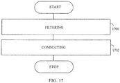
Figure 17 is a flow chart of the operation method. Instep 1700, a signal within the full-bridge inverter 100 is filtered with afirst inductor 152, asecond inductor 158, andthird inductor 176, where
one pin 154 of thefirst inductor 152 being electrically coupled with afirst branch conductor 120, thefirst branch conductor 120 being electrically coupled between the firsthigher switch 106 and the firstlower switch 108, and an opposite pin 156 of thefirst inductor 152 being electrically coupled with afirst output node 190 of the full-bridge inverter 100;
one pin 160 of thesecond inductor 158 being electrically coupled with asecond branch conductor 122, thesecond branch conductor 122 being electrically coupled between the secondhigher switch 110 and the secondlower switch 112, and an opposite pin 162 of thesecond inductor 158 being electrically coupled with asecond output node 192 of the full-bridge inverter 10; and
thethird inductor 176 being electrically coupled between cathodes of afirst diode 166 and asecond diode 168 and anodes of athird diode 172 and afourth diode 174, where thefirst filter diode 166, thesecond filter diode 168 and a secondfiltering unit switch 170 in series are electrically coupled between thefirst branch conductor 120 and thesecond branch conductor 122, cathodes of thefirst diode 166 and thesecond diode 168 are electrically coupled together, and a cathode of thethird diode 172 being electrically coupled with afirst output 190 and a cathode of thefourth diode 174 being electrically coupled with asecond output 192 of the full-bridge inverter 100. - In
step 1702, which is optional, an electric current between thethird inductor 176 and thefirst DC node 10 is conducted throughelectric path circuit 178 in response to switching the firstfiltering unit switch 164 into an electrically conducting state, and an electric current between thethird inductor 176 and thesecond DC node 12 is conducted throughelectric path circuit 184 in response to switching the secondfiltering unit switch 170 into an electrically conducting state. -
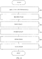
Figure 18 is a flow chart of six stages of the operation method. In afirst stage 1800, switching a firsthigher switch 106 of afirst branch 102 in an electrically conducting state, while a secondelectric path circuit 184 is in an electrically conducting state, for suppressing differential mode ripple and providing a low impedance part for a common mode with afirst inductor 152 and asecond inductor 158. - In a
second stage 1802, switching secondfiltering unit switch 170 into an electrically conducting state, and causing athird inductor 176 to be parallel with asecond inductor 158, and compensating an electric current from thesecond inductor 158 passing through adiode 110B of a secondhigher switch 110 by an electric current flowing through thethird inductor 176 of the filter circuit 150, the electric current flowing through thethird inductor 176 reaching adiode 110B of the secondhigher switch 110 via the secondelectric path circuit 184. - As to an
third stage 1804, causing the full-bridge inverter 100 to enter this stage when the electric current through the secondhigher switch 110 becomes zero, while the electric current flowing through thethird inductor 176 becomes larger than an electric current through thefirst inductor 152 for switching the secondhigher switch 110 in a non-conducting state, and decreasing a strength of the electric current flowing through thethird inductor 176 by a resonance between an inductance of thethird inductor 176, and capacitances of the secondhigher switch 110 and a secondlower switch 112. - As to a
fourth stage 1806, causing the full-bridge inverter 100 to enter in this stage in response to fully charging the capacitance of the secondhigher switch 110 and fully discharging a capacitance of the secondlower switch 112, making thediode 112B of the secondlower switch 112 to electrically conduct at a zero-voltage condition for causing a voltage over thesecond inductor 158 and thethird inductor 176 reverse, and making adiode 108B of a firstlower switch 108 and thediode 112B of the secondlower switch 112 in a non-conducting state in response to the electric current flowing through thethird inductor 176 reaching zero for proceeding to a fifth stage. - As to
fifth stage 1808, causing the full-bridge inverter 100 to enter in this stage in response to the electric current flowing through thethird inductor 176 reaching zero, switching firstlower switch 108 and the secondlower switch 112 in electrically conducting states, filtering using the resonance between the inductance of thethird inductor 176, and the capacitances of the secondhigher switch 110 and a secondlower switch 112 by allowing the secondelectric path circuit 184 be electrically conductive. - In a
sixth stage 1810, switching the secondlower switch 112 in a non-conducting state for ending the zero-voltage condition, shifting to the first stage in response to condition where a voltage over the secondlower switch 112 is equal to an input voltage. - The control of the switches of the full-bridge inverter 100 based on a unipolar switching scheme may be implemented as a logic circuit solution or computer program in order to achieve the operation of the full-bridge inverter 100. The computer program may be placed on a computer program distribution means for the distribution thereof. The computer program distribution means is readable by a data processing device, and it encodes the computer program commands, carries out the operation of the full-bridge inverter 100.
- The computer program may be distributed using a distribution medium which may be any medium readable by the controller. The medium may be a program storage medium, a memory, a software distribution package, or a compressed software package. In some cases, the distribution may be performed using at least one of the following: a near field communication signal, a short distance signal, and a telecommunications signal.
- It will be obvious to a person skilled in the art that, as technology advances, the inventive concept can be implemented in various ways. The invention and its embodiments are not limited to the example embodiments described above but may vary within the scope of the claims.
Claims (8)
- A full-bridge inverter (100) based on a unipolar switching scheme, the full-bridge inverter (100) being configured to convert DC electric power to AC electric power, wherein the full-bridge inverter (100) comprises
a first branch (102) and a second branch (104), which are electrically coupled in parallel between a first DC node (10) and a second DC node (12) of the full-bridge inverter (100) configured to receive the DC electric power, the first branch (102) comprising a first higher switch (106) and a first lower switch (108) in series, and the second branch (104) comprising a second higher switch (110) and a second lower switch (112) in series, characterized in that the full-bridge inverter (100) further comprises
a filter circuit (150) comprising
a first inductor (152), one pin (154) of the first inductor (152) being electrically coupled with a first branch conductor (120), the first branch conductor (120) being electrically coupled between the first higher switch (106) and the first lower switch (108), and an opposite pin (156) of the first inductor (152) being electrically coupled with a first output node (190) of the full-bridge inverter (100);
a second inductor (158), one pin (160) of the second inductor (158) being electrically coupled with a second branch conductor (122), the second branch conductor (122) being electrically coupled between the second higher switch (110) and the second lower switch (112), and an opposite pin (162) of the second inductor (158) being electrically coupled with a second output node (192) of the full-bridge inverter (100);
a first filtering unit switch (164), a first filter diode (166), a second filter diode (168) and a second filtering unit switch (170) in series electrically coupled between the first branch conductor (120) and the second branch conductor (122), cathodes of the first diode (166) and the second diode (168) being electrically coupled together;
a third filter diode (172), whose cathode is electrically coupled with the first output node (190), and a fourth filter diode (174), whose cathode is electrically coupled with the second output node (192), the anodes of the third diode (172) and the fourth diode (174) being electrically coupled together; and
a third inductor (176) electrically coupled between the cathodes of the first diode (166) and the second diode (168) and the anodes of the third diode (172) and the fourth diode (174). - The full-bridge inverter (100) of claim 1, characterized in that full-bridge inverter (100) further comprises electric path circuits (178, 184) configured to conduct an electric current between the third inductor (176) and the first DC node (10) in response to switching the first filtering unit switch (164) in an electrically conducting state, and conduct an electric current between the third inductor (176) and the second DC node (12) in response to switching the second filtering unit switch (170) in an electrically conducting state.
- The full-bridge inverter (100) of claim 1, characterized in that the electric path circuits (178, 184) comprise a first electric path circuit (178) electrically coupled between the second output node (192) and the lower node (12) for conducting an electric current between the third inductor (176) and the second DC node (12), and a second electric path circuit (184) electrically coupled between the first output node (190) and the first DC node (10) for conducting an electric current between the third inductor (176) and the first DC node (10).
- The full-bridge inverter (100) of claim 2 or 3, characterized in that the first electric path circuit (178) comprises a first path switch (180) and a first capacitor (182) in series, the first path switch (180) being configured to switch in an electrically conducting state for conducting an electric current between the third inductor (176) and the first DC node (10), and the second electric path circuit (184) comprises a second path switch (186) and a second capacitor (188) in series, the second path switch (186) being configured to switch in an electrically conducting state for conducting an electric current between the third inductor (176) and the second DC node (12).
- The full-bridge inverter (100) of claim 1, characterized in that the first higher switch (106), and the second higher switch (110) comprises a bipolar junction transistor (106A, 110A) and a reverse biased diode (106B, 110B); and the first lower switch (108) and the second lower switch (112) comprises a field effect transistor (108A, 112A) and a reverse biased diode (108B, 112B).
- A method of operation of a full-bridge inverter (100) based on a unipolar switching scheme, characterized by filtering (1700) a signal within the full-bridge inverter (100) with a first inductor (152), a second inductor (158), and third inductor (176), where
one pin (154) of the first inductor (152) being electrically coupled with a first branch conductor (120), the first branch conductor (120) being electrically coupled between the first higher switch (106) and the first lower switch (108), and an opposite pin (156) of the first inductor (152) being electrically coupled with a first output node (190) of the full-bridge inverter (100);
one pin (160) of the second inductor (158) being electrically coupled with a second branch conductor (122), the second branch conductor (122) being electrically coupled between the second higher switch (110) and the second lower switch (112), and an opposite pin (162) of the second inductor (158) being electrically coupled with a second output node (192) of the full-bridge inverter (100);
the third inductor (176) being electrically coupled between cathodes of a first diode (166) and a second diode (168) and a anodes of a third diode (172) and a fourth diode (174), where the first filter diode (166), the second filter diode (168) and a second filtering unit switch (170) in series are electrically coupled between the first branch conductor (120) and the second branch conductor (122), cathodes of the first diode (166) and the second diode (168) are electrically coupled together, and a cathode of the third diode (172) being electrically coupled with a first output (190) and a cathode of the fourth diode (174) being electrically coupled with a second output (192) of the full-bridge inverter (100); and
conducting (1702), through electric path circuits (178, 184), an electric current between the third inductor (176) and the first DC node (10) in response to switching the first filtering unit switch (164) into an electrically conducting state, and an electric current between the third inductor (176) and the second DC node (12) in response to switching the second filtering unit switch (170) into an electrically conducting state. - The method of claim 6, characterized in by causing the full-bridge inverter (100) to go through the following succeeding operational states in cycles:a first stage (1800) where a first higher switch (106) is in electrically conducting state, the second lower switch (112) and a first filtering unit switch (164) are in an electrically non-conducting state;a second stage (1802) where the first filtering unit switch (164) is in an electrically conducting state causing an electric current flowing through a third inductor (176) to increase until it reaches a same strength as an electric current flowing through a first inductor (152);a third stage (1804) where a reverse diode (110B) of a second higher switch (110) is in an electrically non-conducting state, while capacitance of a second higher switch (110) is discharging, and capacitance of a second lower switch (112) is charging;a fourth stage (1806) where a voltage over the second lower switch (112) is zero and a reverse diode (112B) parallel to the second lower switch (112) conducts electrically, the second lower switch (112) switches into an electrically conducting state before an electric current flowing through the reverse diode (112B) parallel to the second lower switch (112) becomes zero, the third inductor (176) resets and a the first filtering unit switch (164) is switched into an electrically non-conductive state when an electric current flowing through the third inductor (176) is zero;a fifth stage (1808), whose duration depends on a duty cycle of a resonance between an inductance of the third inductor (176), and the capacitances of the second higher switch (110) and a second lower switch (112);a sixth stage (1810) where the second lower switch (112) is in an electrically non-conducting state under a zero-voltage condition, and which ends when a voltage of the second lower switch (112) equals the input voltage of the full-bridge inverter (100).
- The method of claim 6, characterized in that
in a first stage (1800), switching a first higher switch (106) of a first branch (102) in an electrically conducting state, while a second electric path circuit (184) is in an electrically conducting state, for suppressing differential mode ripple and providing a low impedance part for a common mode with a first inductor (152) and a second inductor (158);
in a second stage (1802), switching second filtering unit switch (170) into an electrically conducting state, and causing a third inductor (176) to be parallel with a second inductor (158), and compensating an electric current from the second inductor (158) passing through a diode (110B) of a second higher switch (110) by an electric current flowing through the third inductor (176) of the filter circuit (150), the electric current flowing through the third inductor (176) reaching a diode (110B) of the second higher switch (110) via the second electric path circuit (184);
causing the full-bridge inverter (100) to enter in a third stage (1804) when the electric current through the second higher switch (110) becomes zero, while the electric current flowing through the third inductor (176) becomes larger than an electric current through the first inductor (152) for switching the second higher switch (110) in a non-conducting state, and decreasing a strength of the electric current flowing through the third inductor (176) by a resonance between an inductance of the third inductor (176), and capacitances of the second higher switch (110) and a second lower switch (112);
causing the full-bridge inverter (100) to enter in a fourth stage (1806) in response to fully charging the capacitance of the second higher switch (110) and fully discharging a capacitance of the second lower switch (112), making the diode (112B) of the second lower switch (112) to electrically conduct at a zero-voltage condition for causing a voltage over the second inductor (158) and the third inductor (176) reverse, and making a diode (108B) of a first lower switch (108) and the diode (112B) of the second lower switch (112) in a non-conducting state in response to the electric current flowing through the third inductor (176) reaching zero for proceeding to a fifth stage;
causing the full-bridge inverter (100) to enter in the fifth stage (1808) in response to the electric current flowing through the third inductor (176) reaching zero, switching first lower switch (108) and the second lower switch (112) in electrically conducting states, filtering using the resonance between the inductance of the third inductor (176), and the capacitances of the second higher switch (110) and a second lower switch (112) by allowing the second electric path circuit (184) be electrically conductive; and
in a sixth stage (1810), switching the second lower switch (112) in a non-conducting state for ending the zero-voltage condition, shifting to the first stage in response to condition where a voltage over the second lower switch (112) is equal to an input voltage.
Priority Applications (3)
| Application Number | Priority Date | Filing Date | Title |
|---|---|---|---|
| EP19205300.7A EP3813246B1 (en) | 2019-10-25 | 2019-10-25 | Full-bridge inverter with unipolar switching scheme and its method of operation |
| CN202011149398.7A CN112713792B (en) | 2019-10-25 | 2020-10-23 | Full-bridge inverter with unipolar switching scheme and method of operating the same |
| US17/080,194 US11277078B2 (en) | 2019-10-25 | 2020-10-26 | Full-bridge inverter with unipolar switching scheme and its method of operation |
Applications Claiming Priority (1)
| Application Number | Priority Date | Filing Date | Title |
|---|---|---|---|
| EP19205300.7A EP3813246B1 (en) | 2019-10-25 | 2019-10-25 | Full-bridge inverter with unipolar switching scheme and its method of operation |
Publications (2)
| Publication Number | Publication Date |
|---|---|
| EP3813246A1 true EP3813246A1 (en) | 2021-04-28 |
| EP3813246B1 EP3813246B1 (en) | 2023-09-06 |
Family
ID=68344694
Family Applications (1)
| Application Number | Title | Priority Date | Filing Date |
|---|---|---|---|
| EP19205300.7A Active EP3813246B1 (en) | 2019-10-25 | 2019-10-25 | Full-bridge inverter with unipolar switching scheme and its method of operation |
Country Status (3)
| Country | Link |
|---|---|
| US (1) | US11277078B2 (en) |
| EP (1) | EP3813246B1 (en) |
| CN (1) | CN112713792B (en) |
Families Citing this family (2)
| Publication number | Priority date | Publication date | Assignee | Title |
|---|---|---|---|---|
| KR101957575B1 (en) * | 2017-06-23 | 2019-03-13 | 인투코어테크놀로지 주식회사 | Power supply supporting device and method of supporting power supply to load |
| US11201562B1 (en) * | 2019-06-23 | 2021-12-14 | Purdue Research Foundation | Soft-switching voltage-edge-rate-limiting power inverter |
Citations (2)
| Publication number | Priority date | Publication date | Assignee | Title |
|---|---|---|---|---|
| WO2009156230A2 (en) * | 2008-06-25 | 2009-12-30 | Siemens Ag Österreich | Inverter and method for operating the inverter |
| EP2882090A1 (en) * | 2013-12-05 | 2015-06-10 | ABB Oy | Single-phase fullbridge inverter with switchable output filter |
Family Cites Families (8)
| Publication number | Priority date | Publication date | Assignee | Title |
|---|---|---|---|---|
| US5440209A (en) * | 1978-03-20 | 1995-08-08 | Nilssen; Ole K. | Driven full-bridge inverter ballast |
| US9118259B2 (en) * | 2007-12-03 | 2015-08-25 | Texas Instruments Incorporated | Phase-shifted dual-bridge DC/DC converter with wide-range ZVS and zero circulating current |
| CN102437765B (en) * | 2011-10-17 | 2015-09-23 | 华为技术有限公司 | A kind of inverter topology circuit, inverse method and a kind of inverter |
| CN103051233B (en) * | 2012-12-12 | 2015-02-18 | 东南大学 | Non-isolated single-phase photovoltaic grid-connected inverter and on-off control timing sequence thereof |
| CA2814527C (en) * | 2013-03-15 | 2018-10-23 | Queen's University At Kingston | Single phase power system controller and method therefor |
| TWI488421B (en) * | 2013-04-03 | 2015-06-11 | 台達電子工業股份有限公司 | DC to AC power conversion system and operation method thereof |
| EP3061174B1 (en) * | 2013-10-21 | 2018-04-25 | ABB Schweiz AG | Double-stage inverter apparatus for energy conversion systems and control method thereof |
| US10778106B2 (en) * | 2017-04-24 | 2020-09-15 | Panasonic Intellectual Property Management Co., Ltd. | Power conversion system |
-
2019
- 2019-10-25 EP EP19205300.7A patent/EP3813246B1/en active Active
-
2020
- 2020-10-23 CN CN202011149398.7A patent/CN112713792B/en active Active
- 2020-10-26 US US17/080,194 patent/US11277078B2/en not_active Expired - Fee Related
Patent Citations (2)
| Publication number | Priority date | Publication date | Assignee | Title |
|---|---|---|---|---|
| WO2009156230A2 (en) * | 2008-06-25 | 2009-12-30 | Siemens Ag Österreich | Inverter and method for operating the inverter |
| EP2882090A1 (en) * | 2013-12-05 | 2015-06-10 | ABB Oy | Single-phase fullbridge inverter with switchable output filter |
Non-Patent Citations (5)
| Title |
|---|
| K. M. SMITHK. M. SMEDLEY: "A Comparison of Voltage-Mode Soft-Switching Methods for PWM Converters", IEEE TRANS. POWER ELECTRONICS, vol. 12, no. 2, March 1997 (1997-03-01), pages 376 - 386 |
| KHAN MD NOMAN H ET AL: "Transformerless Inverter Topologies for Single-Phase Photovoltaic Systems: A Comparative Review", IEEE JOURNAL OF EMERGING AND SELECTED TOPICS IN POWER ELECTRONICS, IEEE, PISCATAWAY, NJ, USA, vol. 8, no. 1, 5 April 2019 (2019-04-05), pages 805 - 835, XP011769500, ISSN: 2168-6777, [retrieved on 20200131], DOI: 10.1109/JESTPE.2019.2908672 * |
| L. C. DE. FREITASP. R. C. GOMES: "A High-Frequency ZCS-ZVS-PWM Buck Converter Using a Feedback Resonant Circuit", IEEE TRANS. POWER ELECTRONICS, vol. 10, no. 1, January 1995 (1995-01-01), pages 19 - 24 |
| LI WUHUA ET AL: "Topology Review and Derivation Methodology of Single-Phase Transformerless Photovoltaic Inverters for Leakage Current Suppression", IEEE TRANSACTIONS ON INDUSTRIAL ELECTRONICS, IEEE SERVICE CENTER, PISCATAWAY, NJ, USA, vol. 62, no. 7, 1 July 2015 (2015-07-01), pages 4537 - 4551, XP011581623, ISSN: 0278-0046, [retrieved on 20150515], DOI: 10.1109/TIE.2015.2399278 * |
| M. C. JIANGW. S. WANGH. K. FUK. W. CHANG: "A novel single-phase soft-switching unipolar PWM inverter", PROC. IEEE INTERNATIONAL CONFERENCE ON POWER ELECTRONICS AND ECCE ASIA, 2011, pages 2874 - 2879, XP031956381, DOI: 10.1109/ICPE.2011.5944785 |
Also Published As
| Publication number | Publication date |
|---|---|
| EP3813246B1 (en) | 2023-09-06 |
| CN112713792B (en) | 2023-05-26 |
| CN112713792A (en) | 2021-04-27 |
| US11277078B2 (en) | 2022-03-15 |
| US20210126554A1 (en) | 2021-04-29 |
Similar Documents
| Publication | Publication Date | Title |
|---|---|---|
| US5414613A (en) | Soft switching active snubber for semiconductor circuit operated in discontinuous conduction mode | |
| US20020008981A1 (en) | High frequency sine wave AC Inverter | |
| US10243455B2 (en) | Bidirectional DC-DC converter | |
| US9806629B2 (en) | Single-phase inverter | |
| US20160226479A1 (en) | Converter system, driving circuit and method for semiconductor switch | |
| US20230006540A1 (en) | Power conversion device | |
| US10361624B2 (en) | Multi-cell power converter with improved start-up routine | |
| Fujiwara et al. | A novel lossless passive snubber for soft-switching boost-type converters | |
| US12212221B2 (en) | Power electronic transformer and power supply system | |
| CN103607131A (en) | Neutral point potential balancing control system and method of three-level inverter | |
| EP2882090A1 (en) | Single-phase fullbridge inverter with switchable output filter | |
| US11277078B2 (en) | Full-bridge inverter with unipolar switching scheme and its method of operation | |
| US20240332979A1 (en) | Power conversion system including a second circuit being configured to control a current or power such that the current or the power is synchronized with power ripples caused by the ac power supply or the ac load | |
| CN107819403B (en) | A bipolar soft-switching DC transformer | |
| US20230008233A1 (en) | Ac/dc converter stage for converter system with input series structure with improved common mode performance | |
| CN109039139B (en) | Isolated bidirectional AC/DC conversion circuit and control method thereof | |
| KR20050083812A (en) | Zero-voltage-switching single-switched resonant dc link with minimized conduction loss | |
| CN115765449A (en) | DC conversion circuit and photovoltaic inverter | |
| CN212367151U (en) | Inverter circuit | |
| CN111555648A (en) | an inverter circuit | |
| Seragi et al. | Review on Z-Source Inverter | |
| CN111934572B (en) | Super-large-scale energy storage MMC converter device and energy storage control method | |
| Narimani et al. | A comparative study of three-level DC-DC converters | |
| CN117897883A (en) | Wireless power transmission device for inductive power transmission and method for operating the power transmission device to support zero voltage switching | |
| Khan et al. | Dual-buck three-phase AC-AC converter without commutation problems |
Legal Events
| Date | Code | Title | Description |
|---|---|---|---|
| PUAI | Public reference made under article 153(3) epc to a published international application that has entered the european phase |
Free format text: ORIGINAL CODE: 0009012 |
|
| STAA | Information on the status of an ep patent application or granted ep patent |
Free format text: STATUS: THE APPLICATION HAS BEEN PUBLISHED |
|
| AK | Designated contracting states |
Kind code of ref document: A1 Designated state(s): AL AT BE BG CH CY CZ DE DK EE ES FI FR GB GR HR HU IE IS IT LI LT LU LV MC MK MT NL NO PL PT RO RS SE SI SK SM TR |
|
| AX | Request for extension of the european patent |
Extension state: BA ME |
|
| STAA | Information on the status of an ep patent application or granted ep patent |
Free format text: STATUS: REQUEST FOR EXAMINATION WAS MADE |
|
| 17P | Request for examination filed |
Effective date: 20211022 |
|
| RBV | Designated contracting states (corrected) |
Designated state(s): AL AT BE BG CH CY CZ DE DK EE ES FI FR GB GR HR HU IE IS IT LI LT LU LV MC MK MT NL NO PL PT RO RS SE SI SK SM TR |
|
| RAP1 | Party data changed (applicant data changed or rights of an application transferred) |
Owner name: ABB E-MOBILITY B.V. |
|
| GRAP | Despatch of communication of intention to grant a patent |
Free format text: ORIGINAL CODE: EPIDOSNIGR1 |
|
| STAA | Information on the status of an ep patent application or granted ep patent |
Free format text: STATUS: GRANT OF PATENT IS INTENDED |
|
| INTG | Intention to grant announced |
Effective date: 20230327 |
|
| GRAS | Grant fee paid |
Free format text: ORIGINAL CODE: EPIDOSNIGR3 |
|
| GRAA | (expected) grant |
Free format text: ORIGINAL CODE: 0009210 |
|
| STAA | Information on the status of an ep patent application or granted ep patent |
Free format text: STATUS: THE PATENT HAS BEEN GRANTED |
|
| AK | Designated contracting states |
Kind code of ref document: B1 Designated state(s): AL AT BE BG CH CY CZ DE DK EE ES FI FR GB GR HR HU IE IS IT LI LT LU LV MC MK MT NL NO PL PT RO RS SE SI SK SM TR |
|
| REG | Reference to a national code |
Ref country code: GB Ref legal event code: FG4D |
|
| REG | Reference to a national code |
Ref country code: CH Ref legal event code: EP |
|
| REG | Reference to a national code |
Ref country code: IE Ref legal event code: FG4D |
|
| REG | Reference to a national code |
Ref country code: DE Ref legal event code: R096 Ref document number: 602019036646 Country of ref document: DE |
|
| REG | Reference to a national code |
Ref country code: LT Ref legal event code: MG9D |
|
| REG | Reference to a national code |
Ref country code: NL Ref legal event code: MP Effective date: 20230906 |
|
| PG25 | Lapsed in a contracting state [announced via postgrant information from national office to epo] |
Ref country code: GR Free format text: LAPSE BECAUSE OF FAILURE TO SUBMIT A TRANSLATION OF THE DESCRIPTION OR TO PAY THE FEE WITHIN THE PRESCRIBED TIME-LIMIT Effective date: 20231207 |
|
| PG25 | Lapsed in a contracting state [announced via postgrant information from national office to epo] |
Ref country code: SE Free format text: LAPSE BECAUSE OF FAILURE TO SUBMIT A TRANSLATION OF THE DESCRIPTION OR TO PAY THE FEE WITHIN THE PRESCRIBED TIME-LIMIT Effective date: 20230906 Ref country code: RS Free format text: LAPSE BECAUSE OF FAILURE TO SUBMIT A TRANSLATION OF THE DESCRIPTION OR TO PAY THE FEE WITHIN THE PRESCRIBED TIME-LIMIT Effective date: 20230906 Ref country code: NO Free format text: LAPSE BECAUSE OF FAILURE TO SUBMIT A TRANSLATION OF THE DESCRIPTION OR TO PAY THE FEE WITHIN THE PRESCRIBED TIME-LIMIT Effective date: 20231206 Ref country code: LV Free format text: LAPSE BECAUSE OF FAILURE TO SUBMIT A TRANSLATION OF THE DESCRIPTION OR TO PAY THE FEE WITHIN THE PRESCRIBED TIME-LIMIT Effective date: 20230906 Ref country code: LT Free format text: LAPSE BECAUSE OF FAILURE TO SUBMIT A TRANSLATION OF THE DESCRIPTION OR TO PAY THE FEE WITHIN THE PRESCRIBED TIME-LIMIT Effective date: 20230906 Ref country code: HR Free format text: LAPSE BECAUSE OF FAILURE TO SUBMIT A TRANSLATION OF THE DESCRIPTION OR TO PAY THE FEE WITHIN THE PRESCRIBED TIME-LIMIT Effective date: 20230906 Ref country code: GR Free format text: LAPSE BECAUSE OF FAILURE TO SUBMIT A TRANSLATION OF THE DESCRIPTION OR TO PAY THE FEE WITHIN THE PRESCRIBED TIME-LIMIT Effective date: 20231207 Ref country code: FI Free format text: LAPSE BECAUSE OF FAILURE TO SUBMIT A TRANSLATION OF THE DESCRIPTION OR TO PAY THE FEE WITHIN THE PRESCRIBED TIME-LIMIT Effective date: 20230906 |
|
| REG | Reference to a national code |
Ref country code: AT Ref legal event code: MK05 Ref document number: 1609836 Country of ref document: AT Kind code of ref document: T Effective date: 20230906 |
|
| PG25 | Lapsed in a contracting state [announced via postgrant information from national office to epo] |
Ref country code: NL Free format text: LAPSE BECAUSE OF FAILURE TO SUBMIT A TRANSLATION OF THE DESCRIPTION OR TO PAY THE FEE WITHIN THE PRESCRIBED TIME-LIMIT Effective date: 20230906 |
|
| PG25 | Lapsed in a contracting state [announced via postgrant information from national office to epo] |
Ref country code: IS Free format text: LAPSE BECAUSE OF FAILURE TO SUBMIT A TRANSLATION OF THE DESCRIPTION OR TO PAY THE FEE WITHIN THE PRESCRIBED TIME-LIMIT Effective date: 20240106 |
|
| PG25 | Lapsed in a contracting state [announced via postgrant information from national office to epo] |
Ref country code: AT Free format text: LAPSE BECAUSE OF FAILURE TO SUBMIT A TRANSLATION OF THE DESCRIPTION OR TO PAY THE FEE WITHIN THE PRESCRIBED TIME-LIMIT Effective date: 20230906 |
|
| PG25 | Lapsed in a contracting state [announced via postgrant information from national office to epo] |
Ref country code: ES Free format text: LAPSE BECAUSE OF FAILURE TO SUBMIT A TRANSLATION OF THE DESCRIPTION OR TO PAY THE FEE WITHIN THE PRESCRIBED TIME-LIMIT Effective date: 20230906 |
|
| PG25 | Lapsed in a contracting state [announced via postgrant information from national office to epo] |
Ref country code: SM Free format text: LAPSE BECAUSE OF FAILURE TO SUBMIT A TRANSLATION OF THE DESCRIPTION OR TO PAY THE FEE WITHIN THE PRESCRIBED TIME-LIMIT Effective date: 20230906 Ref country code: RO Free format text: LAPSE BECAUSE OF FAILURE TO SUBMIT A TRANSLATION OF THE DESCRIPTION OR TO PAY THE FEE WITHIN THE PRESCRIBED TIME-LIMIT Effective date: 20230906 Ref country code: IS Free format text: LAPSE BECAUSE OF FAILURE TO SUBMIT A TRANSLATION OF THE DESCRIPTION OR TO PAY THE FEE WITHIN THE PRESCRIBED TIME-LIMIT Effective date: 20240106 Ref country code: ES Free format text: LAPSE BECAUSE OF FAILURE TO SUBMIT A TRANSLATION OF THE DESCRIPTION OR TO PAY THE FEE WITHIN THE PRESCRIBED TIME-LIMIT Effective date: 20230906 Ref country code: EE Free format text: LAPSE BECAUSE OF FAILURE TO SUBMIT A TRANSLATION OF THE DESCRIPTION OR TO PAY THE FEE WITHIN THE PRESCRIBED TIME-LIMIT Effective date: 20230906 Ref country code: CZ Free format text: LAPSE BECAUSE OF FAILURE TO SUBMIT A TRANSLATION OF THE DESCRIPTION OR TO PAY THE FEE WITHIN THE PRESCRIBED TIME-LIMIT Effective date: 20230906 Ref country code: AT Free format text: LAPSE BECAUSE OF FAILURE TO SUBMIT A TRANSLATION OF THE DESCRIPTION OR TO PAY THE FEE WITHIN THE PRESCRIBED TIME-LIMIT Effective date: 20230906 Ref country code: SK Free format text: LAPSE BECAUSE OF FAILURE TO SUBMIT A TRANSLATION OF THE DESCRIPTION OR TO PAY THE FEE WITHIN THE PRESCRIBED TIME-LIMIT Effective date: 20230906 Ref country code: PT Free format text: LAPSE BECAUSE OF FAILURE TO SUBMIT A TRANSLATION OF THE DESCRIPTION OR TO PAY THE FEE WITHIN THE PRESCRIBED TIME-LIMIT Effective date: 20240108 |
|
| PG25 | Lapsed in a contracting state [announced via postgrant information from national office to epo] |
Ref country code: PL Free format text: LAPSE BECAUSE OF FAILURE TO SUBMIT A TRANSLATION OF THE DESCRIPTION OR TO PAY THE FEE WITHIN THE PRESCRIBED TIME-LIMIT Effective date: 20230906 Ref country code: IT Free format text: LAPSE BECAUSE OF FAILURE TO SUBMIT A TRANSLATION OF THE DESCRIPTION OR TO PAY THE FEE WITHIN THE PRESCRIBED TIME-LIMIT Effective date: 20230906 |
|
| REG | Reference to a national code |
Ref country code: CH Ref legal event code: PL |
|
| REG | Reference to a national code |
Ref country code: DE Ref legal event code: R097 Ref document number: 602019036646 Country of ref document: DE |
|
| REG | Reference to a national code |
Ref country code: BE Ref legal event code: MM Effective date: 20231031 |
|
| PG25 | Lapsed in a contracting state [announced via postgrant information from national office to epo] |
Ref country code: LU Free format text: LAPSE BECAUSE OF NON-PAYMENT OF DUE FEES Effective date: 20231025 |
|
| PG25 | Lapsed in a contracting state [announced via postgrant information from national office to epo] |
Ref country code: LU Free format text: LAPSE BECAUSE OF NON-PAYMENT OF DUE FEES Effective date: 20231025 |
|
| PG25 | Lapsed in a contracting state [announced via postgrant information from national office to epo] |
Ref country code: MC Free format text: LAPSE BECAUSE OF FAILURE TO SUBMIT A TRANSLATION OF THE DESCRIPTION OR TO PAY THE FEE WITHIN THE PRESCRIBED TIME-LIMIT Effective date: 20230906 |
|
| PG25 | Lapsed in a contracting state [announced via postgrant information from national office to epo] |
Ref country code: DK Free format text: LAPSE BECAUSE OF FAILURE TO SUBMIT A TRANSLATION OF THE DESCRIPTION OR TO PAY THE FEE WITHIN THE PRESCRIBED TIME-LIMIT Effective date: 20230906 |
|
| PLBE | No opposition filed within time limit |
Free format text: ORIGINAL CODE: 0009261 |
|
| STAA | Information on the status of an ep patent application or granted ep patent |
Free format text: STATUS: NO OPPOSITION FILED WITHIN TIME LIMIT |
|
| PG25 | Lapsed in a contracting state [announced via postgrant information from national office to epo] |
Ref country code: CH Free format text: LAPSE BECAUSE OF NON-PAYMENT OF DUE FEES Effective date: 20231031 |
|
| PG25 | Lapsed in a contracting state [announced via postgrant information from national office to epo] |
Ref country code: MC Free format text: LAPSE BECAUSE OF FAILURE TO SUBMIT A TRANSLATION OF THE DESCRIPTION OR TO PAY THE FEE WITHIN THE PRESCRIBED TIME-LIMIT Effective date: 20230906 Ref country code: DK Free format text: LAPSE BECAUSE OF FAILURE TO SUBMIT A TRANSLATION OF THE DESCRIPTION OR TO PAY THE FEE WITHIN THE PRESCRIBED TIME-LIMIT Effective date: 20230906 Ref country code: CH Free format text: LAPSE BECAUSE OF NON-PAYMENT OF DUE FEES Effective date: 20231031 Ref country code: SI Free format text: LAPSE BECAUSE OF FAILURE TO SUBMIT A TRANSLATION OF THE DESCRIPTION OR TO PAY THE FEE WITHIN THE PRESCRIBED TIME-LIMIT Effective date: 20230906 |
|
| 26N | No opposition filed |
Effective date: 20240607 |
|
| GBPC | Gb: european patent ceased through non-payment of renewal fee |
Effective date: 20231206 |
|
| PG25 | Lapsed in a contracting state [announced via postgrant information from national office to epo] |
Ref country code: BE Free format text: LAPSE BECAUSE OF NON-PAYMENT OF DUE FEES Effective date: 20231031 |
|
| PG25 | Lapsed in a contracting state [announced via postgrant information from national office to epo] |
Ref country code: IE Free format text: LAPSE BECAUSE OF NON-PAYMENT OF DUE FEES Effective date: 20231025 |
|
| PG25 | Lapsed in a contracting state [announced via postgrant information from national office to epo] |
Ref country code: GB Free format text: LAPSE BECAUSE OF NON-PAYMENT OF DUE FEES Effective date: 20231206 |
|
| PG25 | Lapsed in a contracting state [announced via postgrant information from national office to epo] |
Ref country code: FR Free format text: LAPSE BECAUSE OF NON-PAYMENT OF DUE FEES Effective date: 20231106 |
|
| PG25 | Lapsed in a contracting state [announced via postgrant information from national office to epo] |
Ref country code: IE Free format text: LAPSE BECAUSE OF NON-PAYMENT OF DUE FEES Effective date: 20231025 Ref country code: GB Free format text: LAPSE BECAUSE OF NON-PAYMENT OF DUE FEES Effective date: 20231206 Ref country code: FR Free format text: LAPSE BECAUSE OF NON-PAYMENT OF DUE FEES Effective date: 20231106 |
|
| PG25 | Lapsed in a contracting state [announced via postgrant information from national office to epo] |
Ref country code: BG Free format text: LAPSE BECAUSE OF FAILURE TO SUBMIT A TRANSLATION OF THE DESCRIPTION OR TO PAY THE FEE WITHIN THE PRESCRIBED TIME-LIMIT Effective date: 20230906 |
|
| PG25 | Lapsed in a contracting state [announced via postgrant information from national office to epo] |
Ref country code: BG Free format text: LAPSE BECAUSE OF FAILURE TO SUBMIT A TRANSLATION OF THE DESCRIPTION OR TO PAY THE FEE WITHIN THE PRESCRIBED TIME-LIMIT Effective date: 20230906 |
|
| PGFP | Annual fee paid to national office [announced via postgrant information from national office to epo] |
Ref country code: DE Payment date: 20241021 Year of fee payment: 6 |
|
| PG25 | Lapsed in a contracting state [announced via postgrant information from national office to epo] |
Ref country code: CY Free format text: LAPSE BECAUSE OF FAILURE TO SUBMIT A TRANSLATION OF THE DESCRIPTION OR TO PAY THE FEE WITHIN THE PRESCRIBED TIME-LIMIT; INVALID AB INITIO Effective date: 20191025 |
|
| PG25 | Lapsed in a contracting state [announced via postgrant information from national office to epo] |
Ref country code: HU Free format text: LAPSE BECAUSE OF FAILURE TO SUBMIT A TRANSLATION OF THE DESCRIPTION OR TO PAY THE FEE WITHIN THE PRESCRIBED TIME-LIMIT; INVALID AB INITIO Effective date: 20191025 |
|
| PG25 | Lapsed in a contracting state [announced via postgrant information from national office to epo] |
Ref country code: TR Free format text: LAPSE BECAUSE OF FAILURE TO SUBMIT A TRANSLATION OF THE DESCRIPTION OR TO PAY THE FEE WITHIN THE PRESCRIBED TIME-LIMIT Effective date: 20230906 |