EP3809472A1 - A single-photon avalanche diode and a sensor array - Google Patents
A single-photon avalanche diode and a sensor array Download PDFInfo
- Publication number
- EP3809472A1 EP3809472A1 EP20200333.1A EP20200333A EP3809472A1 EP 3809472 A1 EP3809472 A1 EP 3809472A1 EP 20200333 A EP20200333 A EP 20200333A EP 3809472 A1 EP3809472 A1 EP 3809472A1
- Authority
- EP
- European Patent Office
- Prior art keywords
- doped region
- region
- spad
- semiconductor substrate
- lowly
- Prior art date
- Legal status (The legal status is an assumption and is not a legal conclusion. Google has not performed a legal analysis and makes no representation as to the accuracy of the status listed.)
- Granted
Links
Images

Classifications
-
- H—ELECTRICITY
- H10—SEMICONDUCTOR DEVICES; ELECTRIC SOLID-STATE DEVICES NOT OTHERWISE PROVIDED FOR
- H10F—INORGANIC SEMICONDUCTOR DEVICES SENSITIVE TO INFRARED RADIATION, LIGHT, ELECTROMAGNETIC RADIATION OF SHORTER WAVELENGTH OR CORPUSCULAR RADIATION
- H10F77/00—Constructional details of devices covered by this subclass
- H10F77/10—Semiconductor bodies
- H10F77/14—Shape of semiconductor bodies; Shapes, relative sizes or dispositions of semiconductor regions within semiconductor bodies
- H10F77/148—Shapes of potential barriers
-
- H—ELECTRICITY
- H10—SEMICONDUCTOR DEVICES; ELECTRIC SOLID-STATE DEVICES NOT OTHERWISE PROVIDED FOR
- H10F—INORGANIC SEMICONDUCTOR DEVICES SENSITIVE TO INFRARED RADIATION, LIGHT, ELECTROMAGNETIC RADIATION OF SHORTER WAVELENGTH OR CORPUSCULAR RADIATION
- H10F30/00—Individual radiation-sensitive semiconductor devices in which radiation controls the flow of current through the devices, e.g. photodetectors
- H10F30/20—Individual radiation-sensitive semiconductor devices in which radiation controls the flow of current through the devices, e.g. photodetectors the devices having potential barriers, e.g. phototransistors
- H10F30/21—Individual radiation-sensitive semiconductor devices in which radiation controls the flow of current through the devices, e.g. photodetectors the devices having potential barriers, e.g. phototransistors the devices being sensitive to infrared, visible or ultraviolet radiation
- H10F30/22—Individual radiation-sensitive semiconductor devices in which radiation controls the flow of current through the devices, e.g. photodetectors the devices having potential barriers, e.g. phototransistors the devices being sensitive to infrared, visible or ultraviolet radiation the devices having only one potential barrier, e.g. photodiodes
- H10F30/225—Individual radiation-sensitive semiconductor devices in which radiation controls the flow of current through the devices, e.g. photodetectors the devices having potential barriers, e.g. phototransistors the devices being sensitive to infrared, visible or ultraviolet radiation the devices having only one potential barrier, e.g. photodiodes the potential barrier working in avalanche mode, e.g. avalanche photodiodes
-
- H—ELECTRICITY
- H10—SEMICONDUCTOR DEVICES; ELECTRIC SOLID-STATE DEVICES NOT OTHERWISE PROVIDED FOR
- H10F—INORGANIC SEMICONDUCTOR DEVICES SENSITIVE TO INFRARED RADIATION, LIGHT, ELECTROMAGNETIC RADIATION OF SHORTER WAVELENGTH OR CORPUSCULAR RADIATION
- H10F39/00—Integrated devices, or assemblies of multiple devices, comprising at least one element covered by group H10F30/00, e.g. radiation detectors comprising photodiode arrays
- H10F39/10—Integrated devices
- H10F39/107—Integrated devices having multiple elements covered by H10F30/00 in a repetitive configuration, e.g. radiation detectors comprising photodiode arrays
-
- H—ELECTRICITY
- H10—SEMICONDUCTOR DEVICES; ELECTRIC SOLID-STATE DEVICES NOT OTHERWISE PROVIDED FOR
- H10F—INORGANIC SEMICONDUCTOR DEVICES SENSITIVE TO INFRARED RADIATION, LIGHT, ELECTROMAGNETIC RADIATION OF SHORTER WAVELENGTH OR CORPUSCULAR RADIATION
- H10F77/00—Constructional details of devices covered by this subclass
- H10F77/20—Electrodes
- H10F77/206—Electrodes for devices having potential barriers
-
- H—ELECTRICITY
- H10—SEMICONDUCTOR DEVICES; ELECTRIC SOLID-STATE DEVICES NOT OTHERWISE PROVIDED FOR
- H10F—INORGANIC SEMICONDUCTOR DEVICES SENSITIVE TO INFRARED RADIATION, LIGHT, ELECTROMAGNETIC RADIATION OF SHORTER WAVELENGTH OR CORPUSCULAR RADIATION
- H10F77/00—Constructional details of devices covered by this subclass
- H10F77/30—Coatings
- H10F77/306—Coatings for devices having potential barriers
Definitions
- the present disclosure generally relates to the field of light detection. More in particular, the present disclosure relates to light detection using single-photon avalanche diodes, which may be arranged in an array.
- a commonly-used technique for single-photon detection is based on solid-state avalanche photodiodes. Such devices may be operated in the so-called Geiger mode, meaning that individual photo-generated charges are multiplied into detectable charge packets through impact ionization in a large electric field.
- the detector When operating in this mode, the detector may be referred to as a single-photon avalanche diode (SPAD).
- SBA single-photon avalanche diode
- NIR near-infrared
- An objective of the present inventive concept is to provide a single-photon avalanche diode that enables detection of photons with a relatively high uniformity and sensitivity.
- a single-photon avalanche diode for use in a complementary metal-oxide-semiconductor (CMOS) integrated circuit and adapted for detection of light, such as visible or near infrared light
- the SPAD comprising: a semiconductor substrate comprising a top surface at a front side and a back side opposite to the front side; an inner doped region disposed at a top surface of a semiconductor substrate connected to a first terminal, wherein a geometrical structure of a boundary of the inner doped region is rotationally symmetric in a horizontal direction of the semiconductor substrate and wherein the inner doped region comprises dopant implantations of a first type; at least one outer doped region disposed at a top surface of a semiconductor substrate connected to a second terminal, wherein the at least one outer doped region is arranged to at least partially enclose the inner doped region in the horizontal direction of the semiconductor substrate and wherein the outer doped region comprises dopant implantation
- the SPAD according to the first aspect may provide a localized electric field peak which is controlled by the geometry of implants. This implies that there is control over generation of the localized electric field peak, which makes the SPAD relatively insensitive to process variations.
- the SPAD may provide a high photon detection efficiency and may be particularly useful for detection of near infrared light, although the SPAD may also or alternatively be used for detection of other wavelengths.
- the electric field in the depletion volume can be represented by field lines.
- field lines start at an edge of a space charge region near the doped region that is electrically connected to the terminal with the higher potential and end at the edge of the space charge region near the doped region that is electrically connected to the terminal with the lower potential.
- the inner doped region is at least partially enclosed by the outer doped region, the surface of the edge of the space charge region around the inner doped region is smaller than the surface of the edge of the space charge region near outer doped regions and the bottom surface of the lowly doped depletion volume. Consequently, the field line density must be larger near the inner doped region. This results in a local field peak near the inner doped region. Therefore, the geometry of the SPAD may provide a localized electric field peak, which may be approximately uniform, close to the inner doped region which may facilitate light detection.
- a uniform arrangement of the localized electric field peak may be provided around the inner doped region.
- the combined doping profiles of the inner doped region and the outer doped region may be configured such that the field peak around the inner doped region does not extend entirely to an oxide interface at the top surface. Consequently, charges generated on a defective oxide interface have a lower probability of being multiplied. Additionally, charge trapping of carriers generated by an avalanche event is less likely.
- the dopant implantations of the first type are different than the dopant implantations of the second type.
- top surface should be construed as providing a relation of the top surface to other parts of the SPAD.
- the top surface will be an uppermost surface of the semiconductor substrate.
- horizontal direction of the semiconductor substrate should be construed as a direction along or parallel to a main extension of the semiconductor substrate, e.g. parallel to an extension of the top surface.
- a geometrical structure being "rotationally symmetric" should be construed as the geometrical structure having any shape, wherein the geometrical structure is symmetric around a central axis. Since the geometrical structure is symmetric in a horizontal direction, the geometrical structure is symmetric around a central axis being normal to the horizontal direction of the semiconductor substrate.
- At least partially enclose should be interpreted as the at least one outer doped region being arranged around the inner doped region, but the outer doped region need not necessarily form a closed shape that completely encloses the inner doped region. Rather, one or more openings in the shape formed by the at least one outer doped region may be present around the inner doped region.
- the openings in the shape may be symmetrically arranged around the inner doped region with outer doped regions being concentrically arranged around the inner doped region with an equal angular spacing between adjacent outer doped regions.
- the lowly doped depletion volume may be arranged such that the lowly doped depletion volume is arranged between the at least one outer doped region and the inner doped region.
- the at least one outer doped region is arranged to at least partially enclose the inner doped region such that, when the reverse bias is applied to the anode, a surface of a space charge region at the at least one outer doped region is larger than a surface of a space charge region at the inner doped region.
- the at least one outer doped region may be arranged in such manner that the partial enclosing of the inner doped region may ensure that the surface of the space charge region of the at least one outer doped region is larger than the surface of the space charge region at the inner doped region. This implies that it is ensured that the field line density is larger near the inner doped region.
- a ratio of a depth of the lowly doped depletion volume to a horizontal spacing at the top surface between the inner doped region and the outer doped region is in a range of 1-4.
- the depth is too large, full depletion of the lowly doped depletion volume at the breakdown voltage may be difficult to achieve in a vertical direction. If the depth is too small, vertical depletion may occur at a lower voltage than the breakdown voltage.
- a horizontal spacing at the top surface between the inner doped region and the outer doped region is in a range of 2-10 ⁇ m.
- a depth of the lowly doped depletion volume is in a range of 5-30 ⁇ m.
- This may be a suitable depth in order to provide desired characteristics for depletion of the lowly doped depletion volume.
- the boundary of the inner doped region is a surface of a volume in which a dopant concentration is above 1 ⁇ 10 16 cm -3 and wherein the boundary forms a half sphere.
- This may be a suitable dopant concentration. Thanks to the boundary forming a half sphere, uniform field lines around the inner doped region may be formed and the localized electric field peak may be approximately uniform, close to the inner doped region.
- doping gradients at the boundary between the inner doped region and the lowly doped depletion volume is below 1 ⁇ 10 19 cm -3 ⁇ m -1 .
- the doping gradients being small, it may be ensured that no sharp corners or excessively steep doping gradients exist at the boundary between the inner doped region and the lowly doped depletion volume. This enables a localized field peak facilitating impact ionization and Geiger mode multiplication of charges.
- the low doping gradient may be provided exactly at the boundary between the inner doped region and the lowly doped depletion volume, but the low doping gradient may also be provided in proximity of the boundary, such as extending +- 0.1 ⁇ m from the boundary.
- a ratio between a depth and a radius of the rotationally symmetric geometrical structure is in a range of 0.7-1.3.
- the ratio between the depth and the radius of the rotationally symmetric geometrical structure may be around 1.
- the shape of the rotationally symmetric geometrical structure may thus facilitate formation of uniform field lines around the inner doped region.
- a depth of the rotationally symmetric geometrical structure is in a range of 0.3-1.5 ⁇ m and a radius of the rotationally symmetric geometrical structure is in a range of 0.3-1.5 ⁇ m.
- a small size of the rotationally symmetric geometrical structure may enforce local crowding of the electric field lines to form the localized electric field peak.
- the lowly doped depletion volume is configured to extend to a highly doped region at the back side.
- the highly doped region may be commonly connected to the second terminal.
- the highly doped region may have a large thickness such as being up to 1 mm thick.
- the highly doped region may have a dopant concentration above 1 ⁇ 10 18 cm -3 .
- the lowly doped depletion volume may extend to the highly doped region or may transition into the highly doped region through a region of gradually increasing dopant concentration.
- the SPAD is configured for back side illumination, wherein the highly doped region is disposed at a surface of the back side, wherein a thickness of the highly doped region is below 1 ⁇ m and a dopant concentration is above 1 ⁇ 10 18 cm -3 .
- This may be suitable for facilitating detection of light incident at the back side.
- the SPAD is configured for front side illumination
- the highly doped region has a dopant concentration above 1 ⁇ 10 18 cm -3 and has a thickness below 1 mm.
- a doping concentration of the lowly doped depletion volume is below 1 ⁇ 10 14 cm -3 .
- the lowly doped depletion volume may be seen as having a (nearly) intrinsic doping.
- a doping concentration in the lowly doped depletion volume is graded towards a higher doping concentration farther away from the top surface.
- the lowly doped depletion volume may gradually transition into the highly doped region at a back side of the semiconductor substrate.
- the lowly doped depletion volume comprises dopant implantations of p-type.
- This may be a suitable doping of the lowly doped depletion volume.
- doping types may be interchanged.
- the lowly doped depletion volume is depleted to at least 60% of its volume.
- the lowly doped depletion volume provides an at least nearly fully depleted volume.
- the generated carriers may thus move quickly to the inner doped region connected to the first terminal and the outer doped regions connected to the second terminal.
- the inner doped region comprises an innermost region surrounded by an outermost region, wherein the innermost region has a higher doping concentration than the outermost region.
- an outermost region of the inner doped region may present a region which is non-depleted to a high degree at operating conditions.
- the innermost region may have a doping concentration suitable for providing a contact with the first terminal.
- the outermost region defines the boundary of the inner doped region.
- the innermost region is configured to form an ohmic contact with the first terminal. This facilitates a good contact between the inner doped region and the first terminal.
- the inner doped region comprises iso-concentration surfaces that define a doping profile of the inner doped region.
- An outermost iso-concentration surface may also define a boundary of the inner doped region.
- the iso-concentration surfaces of the outermost region of the inner doped region form approximate half spheres for concentrations ranging from 1 ⁇ 10 18 cm -3 to 1 ⁇ 10 16 cm -3 .
- the iso-concentration surface with concentration 1 ⁇ 10 17 cm -3 has a radius in a range of 0.5-1.0 ⁇ m.
- a small size of the rotationally symmetric geometrical structure may be provided to enforce local crowding of the electric field lines to form the localized electric field peak.
- the inner doped region comprises dopant implantations of n-type and wherein the outer doped region comprises dopant implantations of p-type.
- This may be a suitable doping of the inner doped region and the outer doped region.
- doping types may be interchanged.
- each of the at least one outer doped region comprises a highly doped region and a moderately doped region, the highly doped region having a higher doping concentration than the moderately doped region.
- the highly doped region may be provided with a doping concentration suitable for providing a contact with the second terminal.
- the moderately doped region may define a boundary of the outer doped region and may be partially depleted at a transition of the outer doped region to the lowly doped depletion volume.
- the highly doped region is configured to form an ohmic contact with the second terminal. This facilitates a good contact between the outer doped region and the second terminal.
- the moderately doped region is arranged closer to the inner doped region than the highly doped region and wherein the moderately doped region defines the depth of the at least one outer doped region.
- the moderately doped region may be designed with a shape and size such that the lowly doped depletion volume which extends between the outer doped region and the inner doped region may be depleted to a high degree and such that uniform field lines may be formed around the inner doped region.
- the outer doped region comprises iso-concentration surfaces that define a doping profile of the outer doped region.
- An outermost iso-concentration surface may also define a boundary of the outer doped region.
- a distance between the top surface and the back side is larger than a smallest distance between a center of the inner doped region and an iso-concentration surface with concentration 1 ⁇ 10 17 cm -3 in the outer doped region by a factor between 1 and 4.
- the lowly doped depletion volume may extend in a major portion of the distance between the top surface and the back side. If the distance is too large, full depletion of the lowly doped depletion volume at the breakdown voltage may be difficult to achieve in a vertical direction. If the distance is too small, vertical depletion may occur at a lower voltage than the breakdown voltage.
- the depth of the outer doped region is in a range of 0.5-3.5 ⁇ m.
- the outer doped region may relate to the inner doped region for forming uniform field lines around the inner doped region.
- the outer doped region comprises a portion bulging inwards from the top surface.
- the portion bulging inwards may ensure that the distance between the inner and outer doped region increases near the top surface, which may ensure that localized field peak does not extend to the top surface.
- the SPAD further comprises a shallow lowly doped region at the top surface between the inner doped region and the outer doped region and above the lowly doped depletion volume.
- the shallow lowly doped region comprises dopant implantations of the first type and has a doping concentration in a range of 1 ⁇ 10 12 cm -3 to 1 ⁇ 10 15 cm -3 .
- the shallow lowly doped region may also be configured in relation to an effect of the shallow lowly doped region on electric field lines in a remainder of the SPAD.
- the shallow lowly doped region has a thickness that is smaller than 200 nm.
- This may be a suitable thickness of the shallow lowly doped region in order for the shallow lowly doped region to reduce localized filed peak only at the top surface of the semiconductor substrate.
- the SPAD is configured such that, when the reverse bias is applied to the second terminal and the back side of the semiconductor substrate, the electric field peak does not extend to the top surface.
- the shallow lowly doped region may be depleted by more than 90% of its volume. Thus, charges generated on a defective interface between the top surface and an oxide above have a lower probability of being multiplied. Additionally, charge trapping of carriers generated by an avalanche event is less likely.
- the SPAD is configured such that, when a reverse bias of 50V is applied to the anode, the electric field peak enabling impact ionization and multiplication of charges is formed.
- the electric field peak may be formed while applying a relatively small voltage of 50V. It should be realized that the electric field peak may be formed with even lower voltages being applied, but the electric field peak should at least be formed when a reverse bias of 50V is applied to the anode.
- the SPAD further comprises a top layer of silicon dioxide arranged above the top surface of the semiconductor substrate, wherein connections between the inner doped region and the first terminal and between the at least one outer doped region and the second terminal extend through the top layer.
- the top layer of silicon dioxide may ensure electric isolation between the first and second terminals. Further, it should be realized that other materials than silicon dioxide may be used.
- the at least one outer doped region is configured to completely enclose the inner doped region in the horizontal direction of the semiconductor substrate.
- the at least one outer doped region is configured to circularly enclose the inner doped region.
- the at least one outer region comprises a plurality of outer regions, wherein the plurality of outer regions together enclose the inner doped region forming an n-fold symmetry around the inner doped region, where n > 3.
- the plurality of regions may be arranged symmetrically around the inner doped region.
- the plurality of regions may be equally spaced on a circular line concentric with the inner doped region.
- a spacing may be provided between adjacent outer doped regions, while the outer doped regions do not fully enclose the inner doped region.
- the arrangement may still ensure that uniform field lines are formed around the inner doped region and may facilitate that a localized electric field peak is formed.
- a sensor array comprising: an array of single-photon avalanche diodes, SPADs, wherein each SPAD in the array of SPADs is a SPAD according to the first aspect; wherein the second terminals of each of the SPADs are commonly connected.
- the second terminals may be commonly connected, which reduces the number of connections to the array of SPADs.
- the first terminals of each of the SPADs are separately connected for separate read-out of light detected by each of the SPADs.
- the second terminals may be commonly connected, the first terminals being separately connected still ensures that each of the SPADs may be separately read out for two-dimensional imaging.
- the outer regions of each of the SPADs are shared and form a single coherent region.
- This may be a simple manner of forming the outer regions, as the outer regions of different SPADs need not necessarily be separated from each other.
- an outer region may be shared by more than one SPAD.
- a deep trench isolation structure is provided between each pair of adjacent SPADs in the array of SPADs.
- lowly doped depletion volumes of adjacent SPADs transition into each other and a lowly doped depletion volume belonging to an individual SPAD is defined by a pitch of the array of SPADs.
- the individual SPADs may be defined by the arrangement of the outer doped regions and inner doped regions such that field lines are defined within the individual SPADs and crosstalk is avoided.
- Fig. 1 is based on Figure 1 of Takai, Isamu, et al. "Single-photon avalanche diode with enhanced NIR-sensitivity for automotive LIDAR systems.”, Sensors 16.4 (2016): 459 .
- NIR-enhanced SPADs 100 rely on deep pn-junctions formed by stacked p-type 103 and n-type 102 implants. They are fabricated in a CMOS compatible platform with limited custom processing steps.
- the guard ring surrounding the junctions is relatively simple and small, and the SPADs can be integrated into dense arrays.
- An example of the doping profile of such a device is given in Fig. 1 .
- the junction contains a laterally uniform high-field region parallel to the top device interface. This approach has two shortcomings:
- Fig. 2 is based on the Figure on page 1 of Grubi ⁇ i ⁇ , D., and A. Shah. "New silicon reach-through avalanche photodiodes with enhanced sensitivity in the DUV/UV wavelength range.” 2013 36th International Convention on Information and Communication Technology, Electronics and Microelectronics (MIPRO). IEEE, 2013 .
- the absorption depth may be increased to tens of microns by introducing a deep absorption region 200 below the top pn-junction as demonstrated in Fig. 2 .
- the device is now called a reach through SPAD.
- the absorption region is lowly doped and fully depleted such that generated carriers are transported quickly towards the multiplication field.
- the main junction is still formed by dedicated p-type implants 204 and n-type implants 202 parallel to the top interface.
- the high field region remains contained within this junction.
- the addition of the thick depleted region results in additional shortcomings:
- planar silicon NIR-enhanced SPAD designs rely on the doping profile of some sort of pn- or pin-junction for the formation of the multiplication field. Active measures are taken to prevent premature breakdown at the junction edges.
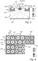
- Fig. 3 demonstrates the doping profile and electric field of a planar silicon SPAD based on separate absorption and multiplication (SAM).
- the doping profile consists of multiple inner n-type doping implantations 300 and outer p-type doping implantations 302 for the formation of the cathode and anode respectively.
- the anode encloses the cathode in the horizontal cross-section near the top oxide interface 304.
- the cathode and anode are separated by a lowly doped p-type 306 (nearly) fully depleted volume which extends up to tens of microns deep.
- the lowly doped volume terminates at the back of the device 308.
- the anode is reverse biased above the breakdown voltage, and the backside 308 is biased at the same voltage as the anode.
- a dedicated doping implant for creating the multiplication field is absent. Consequently, the device relies on the geometry of the implants for the formation of a localized uniform field peak 312 near the cathode, rather than on the doping profile of a steep pn-junction. More specifically, the geometry enforces the crowding of the electric field lines 310, 312 near the cathode, as demonstrated in Fig. 3 .
- the field peak 312 is spherically uniform around the cathode but remains spaced away from the oxide interface.
- the device is illuminated from the backside 308, so called backside illumination (BSI) 308.
- BSI backside illumination
- the device may alternatively be illuminated from a frontside 316, so called frontside illumination (FSI).
- FSI frontside illumination
- the device is intended for the integration into large uniform monolithic arrays wherein all anodes are commonly connected, and each cathode is connected to a separate readout circuit. Doping types may be interchanged. If so, the cathodes are commonly connected while the anodes are separately read out.
- a single SPAD in an array can be described generically as follows:
- the SPAD detector may have the following properties and features (in no particular order):
- the device employs a geometry-constrained uniform field peak 312 around a narrow central doped region 300.
- the field extends into a deep lowly doped region 306.
- this allows for higher NIR photon detection efficiency, near-unity BSI fill factor, acceptable breakdown voltage and lower sensitivity to process variations.
- the time resolution also remains acceptable for time-of-flight applications.
- the inner doped region 300 may be small and rotationally symmetric to allow for an approximately spherically uniform field peak 312.
- the outer doped region 306 need not necessarily comply with specific symmetries, as long as the shape does not affect the uniformity of the field peak 312 and allows for efficient depletion and a low breakdown voltage.
- Fig. 4 demonstrates a non-exhaustive set of horizontal cross sections near the top interface of possible arrangements 400, 402, 404, 406, 408 of the doped regions in an array of SPADs.
- the arrangement 400 may be preferred.
- Deep trench isolation (DTI) 440 may be employed to reduce optical crosstalk.
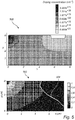
- Fig. 5 shows the doping profile 500 in a top graph of Fig. 5 , a normalized electric field 502 and depletion region 504 in a bottom graph of Fig. 5 near the top device interface in a relatively well-optimized design.
Landscapes
- Light Receiving Elements (AREA)
Abstract
Description
- The present disclosure generally relates to the field of light detection. More in particular, the present disclosure relates to light detection using single-photon avalanche diodes, which may be arranged in an array.
- A commonly-used technique for single-photon detection is based on solid-state avalanche photodiodes. Such devices may be operated in the so-called Geiger mode, meaning that individual photo-generated charges are multiplied into detectable charge packets through impact ionization in a large electric field. When operating in this mode, the detector may be referred to as a single-photon avalanche diode (SPAD). For many applications, including for example range-finding, detecting near-infrared (NIR) radiation with high efficiency using such SPAD detectors may be important.
- To exploit well-established semiconductor processing platforms, and to simplify on-chip integration of CMOS circuitry, there may be a strong interest in developing and fabricating arrays of such SPADs in silicon. However, due to the low energy (∼1eV) of NIR radiation, silicon provides a small absorption coefficient for such radiation. Therefore, a large depleted volume may be required in addition to a large electric field. This may introduce trade-offs between detection speed, noise, uniformity, and sensitivity. Implementing arrays of SPADs in silicon may thus be challenging.
- An objective of the present inventive concept is to provide a single-photon avalanche diode that enables detection of photons with a relatively high uniformity and sensitivity.
- These and other objects of the invention are at least partly met by the invention as defined in the independent claims. Preferred embodiments are set out in the dependent claims.
- According to a first aspect of the present inventive concept, there is provided a single-photon avalanche diode (SPAD) for use in a complementary metal-oxide-semiconductor (CMOS) integrated circuit and adapted for detection of light, such as visible or near infrared light, the SPAD comprising: a semiconductor substrate comprising a top surface at a front side and a back side opposite to the front side; an inner doped region disposed at a top surface of a semiconductor substrate connected to a first terminal, wherein a geometrical structure of a boundary of the inner doped region is rotationally symmetric in a horizontal direction of the semiconductor substrate and wherein the inner doped region comprises dopant implantations of a first type; at least one outer doped region disposed at a top surface of a semiconductor substrate connected to a second terminal, wherein the at least one outer doped region is arranged to at least partially enclose the inner doped region in the horizontal direction of the semiconductor substrate and wherein the outer doped region comprises dopant implantations of a second type; a lowly doped depletion volume, which is arranged to surround the rotationally symmetric inner doped region and which comprises dopant implantations of the first type or dopant implantations of the second type; wherein a depth of the lowly doped depletion volume extending from the top surface of the semiconductor substrate into the semiconductor substrate is larger than a depth of the at least one outer doped region, wherein the second terminal and the back side of the semiconductor substrate are commonly connected, and wherein one of the first and the second terminal forms an anode and another of the first and the second terminal forms a cathode; and wherein the SPAD is configured such that, when a reverse bias is applied to the anode, an electric field peak around the inner doped region is formed to enable impact ionization and multiplication of charges.
- The SPAD according to the first aspect may provide a localized electric field peak which is controlled by the geometry of implants. This implies that there is control over generation of the localized electric field peak, which makes the SPAD relatively insensitive to process variations.
- Further, the SPAD may provide a high photon detection efficiency and may be particularly useful for detection of near infrared light, although the SPAD may also or alternatively be used for detection of other wavelengths.
- The electric field in the depletion volume can be represented by field lines. When a reverse bias is applied, field lines start at an edge of a space charge region near the doped region that is electrically connected to the terminal with the higher potential and end at the edge of the space charge region near the doped region that is electrically connected to the terminal with the lower potential. Because the inner doped region is at least partially enclosed by the outer doped region, the surface of the edge of the space charge region around the inner doped region is smaller than the surface of the edge of the space charge region near outer doped regions and the bottom surface of the lowly doped depletion volume. Consequently, the field line density must be larger near the inner doped region. This results in a local field peak near the inner doped region. Therefore, the geometry of the SPAD may provide a localized electric field peak, which may be approximately uniform, close to the inner doped region which may facilitate light detection.
- Thanks to the boundary of the inner doped region being rotationally symmetric, a uniform arrangement of the localized electric field peak may be provided around the inner doped region.
- Thanks to the arrangement of the SPAD, the combined doping profiles of the inner doped region and the outer doped region may be configured such that the field peak around the inner doped region does not extend entirely to an oxide interface at the top surface. Consequently, charges generated on a defective oxide interface have a lower probability of being multiplied. Additionally, charge trapping of carriers generated by an avalanche event is less likely.
- The dopant implantations of the first type are different than the dopant implantations of the second type.
- As used herein, "top surface" should be construed as providing a relation of the top surface to other parts of the SPAD. Thus, when the semiconductor substrate is oriented with the front side facing upwards, the top surface will be an uppermost surface of the semiconductor substrate. However, it should further be realized that there may be other structures arranged on or above the "top surface", such that the "top surface" need not necessarily be an uppermost surface of the SPAD.
- As used herein, "horizontal direction of the semiconductor substrate" should be construed as a direction along or parallel to a main extension of the semiconductor substrate, e.g. parallel to an extension of the top surface.
- As used herein, a geometrical structure being "rotationally symmetric" should be construed as the geometrical structure having any shape, wherein the geometrical structure is symmetric around a central axis. Since the geometrical structure is symmetric in a horizontal direction, the geometrical structure is symmetric around a central axis being normal to the horizontal direction of the semiconductor substrate.
- As used herein, "at least partially enclose" should be interpreted as the at least one outer doped region being arranged around the inner doped region, but the outer doped region need not necessarily form a closed shape that completely encloses the inner doped region. Rather, one or more openings in the shape formed by the at least one outer doped region may be present around the inner doped region. The openings in the shape may be symmetrically arranged around the inner doped region with outer doped regions being concentrically arranged around the inner doped region with an equal angular spacing between adjacent outer doped regions.
- The lowly doped depletion volume may be arranged such that the lowly doped depletion volume is arranged between the at least one outer doped region and the inner doped region.
- According to an embodiment, the at least one outer doped region is arranged to at least partially enclose the inner doped region such that, when the reverse bias is applied to the anode, a surface of a space charge region at the at least one outer doped region is larger than a surface of a space charge region at the inner doped region.
- Hence, the at least one outer doped region may be arranged in such manner that the partial enclosing of the inner doped region may ensure that the surface of the space charge region of the at least one outer doped region is larger than the surface of the space charge region at the inner doped region. This implies that it is ensured that the field line density is larger near the inner doped region.
- According to an embodiment, a ratio of a depth of the lowly doped depletion volume to a horizontal spacing at the top surface between the inner doped region and the outer doped region is in a range of 1-4.
- If the depth is too large, full depletion of the lowly doped depletion volume at the breakdown voltage may be difficult to achieve in a vertical direction. If the depth is too small, vertical depletion may occur at a lower voltage than the breakdown voltage.
- According to an embodiment, a horizontal spacing at the top surface between the inner doped region and the outer doped region is in a range of 2-10 µm.
- If the spacing is too large, full depletion of the lowly doped depletion volume at the breakdown voltage may be difficult to achieve in the horizontal direction. If the depth is too small, horizontal depletion may occur at a lower voltage than the breakdown voltage.
- According to an embodiment, a depth of the lowly doped depletion volume is in a range of 5-30 µm.
- This may be a suitable depth in order to provide desired characteristics for depletion of the lowly doped depletion volume.
- According to an embodiment, the boundary of the inner doped region is a surface of a volume in which a dopant concentration is above 1∗1016 cm-3 and wherein the boundary forms a half sphere.
- This may be a suitable dopant concentration. Thanks to the boundary forming a half sphere, uniform field lines around the inner doped region may be formed and the localized electric field peak may be approximately uniform, close to the inner doped region.
- According to an embodiment, doping gradients at the boundary between the inner doped region and the lowly doped depletion volume is below 1∗1019 cm-3 µm-1.
- Thanks to the doping gradients being small, it may be ensured that no sharp corners or excessively steep doping gradients exist at the boundary between the inner doped region and the lowly doped depletion volume. This enables a localized field peak facilitating impact ionization and Geiger mode multiplication of charges.
- The low doping gradient may be provided exactly at the boundary between the inner doped region and the lowly doped depletion volume, but the low doping gradient may also be provided in proximity of the boundary, such as extending +- 0.1 µm from the boundary.
- According to an embodiment, a ratio between a depth and a radius of the rotationally symmetric geometrical structure is in a range of 0.7-1.3.
- The ratio between the depth and the radius of the rotationally symmetric geometrical structure may be around 1.
- The shape of the rotationally symmetric geometrical structure may thus facilitate formation of uniform field lines around the inner doped region.
- According to an embodiment, a depth of the rotationally symmetric geometrical structure is in a range of 0.3-1.5 µm and a radius of the rotationally symmetric geometrical structure is in a range of 0.3-1.5 µm.
- A small size of the rotationally symmetric geometrical structure may enforce local crowding of the electric field lines to form the localized electric field peak.
- According to an embodiment, the lowly doped depletion volume is configured to extend to a highly doped region at the back side.
- The highly doped region may be commonly connected to the second terminal. The highly doped region may have a large thickness such as being up to 1 mm thick. The highly doped region may have a dopant concentration above 1∗1018 cm-3.
- The lowly doped depletion volume may extend to the highly doped region or may transition into the highly doped region through a region of gradually increasing dopant concentration.
- According to an embodiment, the SPAD is configured for back side illumination, wherein the highly doped region is disposed at a surface of the back side, wherein a thickness of the highly doped region is below 1 µm and a dopant concentration is above 1∗1018 cm-3.
- This may be suitable for facilitating detection of light incident at the back side.
- According to an embodiment, the SPAD is configured for front side illumination, the highly doped region has a dopant concentration above 1∗1018 cm-3 and has a thickness below 1 mm.
- This may facilitate that light incident on the back side of the semiconductor substrate does not affect detection of front side illumination.
- According to an embodiment, a doping concentration of the lowly doped depletion volume is below 1∗1014 cm-3.
- This implies that very few dopant implantations are present in the lowly doped depletion volume. The lowly doped depletion volume may be seen as having a (nearly) intrinsic doping.
- According to an embodiment, a doping concentration in the lowly doped depletion volume is graded towards a higher doping concentration farther away from the top surface.
- Thus, the lowly doped depletion volume may gradually transition into the highly doped region at a back side of the semiconductor substrate.
- According to an embodiment, the lowly doped depletion volume comprises dopant implantations of p-type.
- This may be a suitable doping of the lowly doped depletion volume. However, doping types may be interchanged.
- According to an embodiment, the lowly doped depletion volume is depleted to at least 60% of its volume.
- This implies that the lowly doped depletion volume provides an at least nearly fully depleted volume. The generated carriers may thus move quickly to the inner doped region connected to the first terminal and the outer doped regions connected to the second terminal.
- According to an embodiment, the inner doped region comprises an innermost region surrounded by an outermost region, wherein the innermost region has a higher doping concentration than the outermost region.
- This implies that an outermost region of the inner doped region may present a region which is non-depleted to a high degree at operating conditions. The innermost region may have a doping concentration suitable for providing a contact with the first terminal.
- According to an embodiment, the outermost region defines the boundary of the inner doped region.
- According to an embodiment, the innermost region is configured to form an ohmic contact with the first terminal. This facilitates a good contact between the inner doped region and the first terminal.
- According to an embodiment, the inner doped region comprises iso-concentration surfaces that define a doping profile of the inner doped region. An outermost iso-concentration surface may also define a boundary of the inner doped region.
- According to an embodiment, the iso-concentration surfaces of the outermost region of the inner doped region form approximate half spheres for concentrations ranging from 1∗1018 cm-3 to 1∗1016 cm-3.
- Thus, forming of uniform field lines around the inner doped region may be facilitated.
- According to an embodiment, the iso-concentration surface with
concentration 1∗1017 cm-3 has a radius in a range of 0.5-1.0 µm. - Thus, a small size of the rotationally symmetric geometrical structure may be provided to enforce local crowding of the electric field lines to form the localized electric field peak.
- According to an embodiment, the inner doped region comprises dopant implantations of n-type and wherein the outer doped region comprises dopant implantations of p-type.
- This may be a suitable doping of the inner doped region and the outer doped region. However, doping types may be interchanged.
- According to an embodiment, each of the at least one outer doped region comprises a highly doped region and a moderately doped region, the highly doped region having a higher doping concentration than the moderately doped region.
- This implies that the highly doped region may be provided with a doping concentration suitable for providing a contact with the second terminal. The moderately doped region may define a boundary of the outer doped region and may be partially depleted at a transition of the outer doped region to the lowly doped depletion volume.
- According to an embodiment, the highly doped region is configured to form an ohmic contact with the second terminal. This facilitates a good contact between the outer doped region and the second terminal.
- According to an embodiment, the moderately doped region is arranged closer to the inner doped region than the highly doped region and wherein the moderately doped region defines the depth of the at least one outer doped region.
- The moderately doped region may be designed with a shape and size such that the lowly doped depletion volume which extends between the outer doped region and the inner doped region may be depleted to a high degree and such that uniform field lines may be formed around the inner doped region.
- According to an embodiment, the outer doped region comprises iso-concentration surfaces that define a doping profile of the outer doped region. An outermost iso-concentration surface may also define a boundary of the outer doped region.
- According to an embodiment, a distance between the top surface and the back side is larger than a smallest distance between a center of the inner doped region and an iso-concentration surface with
concentration 1∗1017 cm-3 in the outer doped region by a factor between 1 and 4. - The lowly doped depletion volume may extend in a major portion of the distance between the top surface and the back side. If the distance is too large, full depletion of the lowly doped depletion volume at the breakdown voltage may be difficult to achieve in a vertical direction. If the distance is too small, vertical depletion may occur at a lower voltage than the breakdown voltage.
- According to an embodiment, the depth of the outer doped region is in a range of 0.5-3.5 µm.
- This implies that the outer doped region may relate to the inner doped region for forming uniform field lines around the inner doped region.
- According to an embodiment, the outer doped region comprises a portion bulging inwards from the top surface.
- This may be beneficial in ensuring that charge trapping at the top surface of carriers generated by an avalanche event is less likely. The portion bulging inwards may ensure that the distance between the inner and outer doped region increases near the top surface, which may ensure that localized field peak does not extend to the top surface.
- According to an embodiment, the SPAD further comprises a shallow lowly doped region at the top surface between the inner doped region and the outer doped region and above the lowly doped depletion volume.
- This may further reduce a localized field peak at the top surface.
- According to an embodiment, the shallow lowly doped region comprises dopant implantations of the first type and has a doping concentration in a range of 1∗1012 cm-3 to 1∗1015 cm-3.
- This may be a suitable doping concentration of the shallow lowly doped region. The shallow lowly doped region may also be configured in relation to an effect of the shallow lowly doped region on electric field lines in a remainder of the SPAD.
- According to an embodiment, the shallow lowly doped region has a thickness that is smaller than 200 nm.
- This may be a suitable thickness of the shallow lowly doped region in order for the shallow lowly doped region to reduce localized filed peak only at the top surface of the semiconductor substrate.
- According to an embodiment, the SPAD is configured such that, when the reverse bias is applied to the second terminal and the back side of the semiconductor substrate, the electric field peak does not extend to the top surface. The shallow lowly doped region may be depleted by more than 90% of its volume. Thus, charges generated on a defective interface between the top surface and an oxide above have a lower probability of being multiplied. Additionally, charge trapping of carriers generated by an avalanche event is less likely.
- According to an embodiment, the SPAD is configured such that, when a reverse bias of 50V is applied to the anode, the electric field peak enabling impact ionization and multiplication of charges is formed.
- This implies that the electric field peak may be formed while applying a relatively small voltage of 50V. It should be realized that the electric field peak may be formed with even lower voltages being applied, but the electric field peak should at least be formed when a reverse bias of 50V is applied to the anode.
- According to an embodiment, the SPAD further comprises a top layer of silicon dioxide arranged above the top surface of the semiconductor substrate, wherein connections between the inner doped region and the first terminal and between the at least one outer doped region and the second terminal extend through the top layer.
- The top layer of silicon dioxide may ensure electric isolation between the first and second terminals. Further, it should be realized that other materials than silicon dioxide may be used.
- According to an embodiment, the at least one outer doped region is configured to completely enclose the inner doped region in the horizontal direction of the semiconductor substrate.
- This may facilitate that uniform field lines may be formed around an entire circumference of the inner doped region, as the outer doped region completely encloses the inner doped region.
- According to an embodiment, the at least one outer doped region is configured to circularly enclose the inner doped region.
- This may further facilitate that uniform field lines are formed around the inner doped region.
- According to an embodiment, the at least one outer region comprises a plurality of outer regions, wherein the plurality of outer regions together enclose the inner doped region forming an n-fold symmetry around the inner doped region, where n > 3.
- Thus, the plurality of regions may be arranged symmetrically around the inner doped region. The plurality of regions may be equally spaced on a circular line concentric with the inner doped region. With such arrangement, a spacing may be provided between adjacent outer doped regions, while the outer doped regions do not fully enclose the inner doped region. The arrangement may still ensure that uniform field lines are formed around the inner doped region and may facilitate that a localized electric field peak is formed.
- According to a second aspect, there is provided a sensor array, comprising: an array of single-photon avalanche diodes, SPADs, wherein each SPAD in the array of SPADs is a SPAD according to the first aspect; wherein the second terminals of each of the SPADs are commonly connected.
- Effects and features of this second aspect are largely analogous to those described above in connection with the first aspect. Embodiments mentioned in relation to the first aspect are largely compatible with the second aspect.
- Thanks to having an array of SPADs, two-dimensional imaging using the SPADs is enabled.
- The second terminals may be commonly connected, which reduces the number of connections to the array of SPADs.
- According to an embodiment, the first terminals of each of the SPADs are separately connected for separate read-out of light detected by each of the SPADs.
- Thus, while the second terminals may be commonly connected, the first terminals being separately connected still ensures that each of the SPADs may be separately read out for two-dimensional imaging.
- According to an embodiment, the outer regions of each of the SPADs are shared and form a single coherent region.
- This may be a simple manner of forming the outer regions, as the outer regions of different SPADs need not necessarily be separated from each other.
- Also, in some embodiments, such as when a plurality of outer regions is provided, an outer region may be shared by more than one SPAD.
- According to an embodiment, a deep trench isolation structure is provided between each pair of adjacent SPADs in the array of SPADs.
- This may reduce optical crosstalk between adjacent SPADs.
- According to an embodiment, lowly doped depletion volumes of adjacent SPADs transition into each other and a lowly doped depletion volume belonging to an individual SPAD is defined by a pitch of the array of SPADs.
- This may facilitate forming of the lowly doped depletion volume. The individual SPADs may be defined by the arrangement of the outer doped regions and inner doped regions such that field lines are defined within the individual SPADs and crosstalk is avoided.
- The above, as well as additional objects, features and advantages of the present inventive concept, will be better understood through the following illustrative and non-limiting detailed description, with reference to the appended drawings. In the drawings like reference numerals will be used for like elements unless stated otherwise.
-
Fig. 1 shows a cross-section of the doping profile of a prior art planar NIR-enhanced SPAD as disclosed in Takai, Isamu, et al. "Single-photon avalanche diode with enhanced NIR-sensitivity for automotive LIDAR systems." Sensors 16.4 (2016): 459. -
Fig. 2 shows a cross-section of the doping profile of a reach through prior art NIR-enhanced SPAD as disclosed in Grubiš̌̌ić, D., and A. Shah. "New silicon reach-through avalanche photodiodes with enhanced sensitivity in the DUV/UV wavelength range." 2013 36th International Convention on Information and Communication Technology, Electronics and Microelectronics (MIPRO). IEEE, 2013. -
Fig. 3 shows a cross-section of the doping profile of one embodiment of a NIR-enhanced SPAD with a geometry-constrained field peak around a rotationally symmetric inner doped region. Field lines and the multiplication region are indicated. -
Fig. 4 shows a non-exhaustive set of horizontal cross-sections of possible arrangement of different device regions in a NIR-enhanced SPAD array with geometry-constrained field peaks. -
Fig. 5 shows a doping profile, normalized electric field and depletion region edge near a top interface of a SPAD with a geometry-constrained field. The rotationally symmetric axis is located at x = 0 µm. - There is a strong interest in the development of SPAD arrays in silicon. This allows for the exploitation of well-established semiconductor processing platforms and simplifies the on-chip integration of CMOS circuitry. Furthermore, silicon detectors generally exhibit better noise characteristics than germanium and III-V counterparts. However, a large disadvantage of silicon is the low NIR absorption coefficient, and therefore a low photon detection probability (PDP).
- Reference is now made to
Fig. 1 , which is based onFigure 1 of Takai, Isamu, et al. "Single-photon avalanche diode with enhanced NIR-sensitivity for automotive LIDAR systems.", Sensors 16.4 (2016): 459. Typically, NIR-enhancedSPADs 100 rely on deep pn-junctions formed by stacked p-type 103 and n-type 102 implants. They are fabricated in a CMOS compatible platform with limited custom processing steps. The guard ring surrounding the junctions is relatively simple and small, and the SPADs can be integrated into dense arrays. An example of the doping profile of such a device is given inFig. 1 . The junction contains a laterally uniform high-field region parallel to the top device interface. This approach has two shortcomings: - The absorption depth remains limited to a couple of microns. As a result, the single photon detection efficiency is typically not larger than 10 % at 905 nm.
- Carriers absorbed on the sides of the junction have a lower detection probability, as they may not be transported through the high-field region or recombine too soon. This limits the photon detection efficiency of SPADs integrated into arrays. The size of the peripheral region is determined by the size of the guard ring, device contacts and any additional in-pixel circuits.
- Reference is now made to
Fig. 2 , which is based on the Figure onpage 1 of Grubiš̌ić, D., and A. Shah. "New silicon reach-through avalanche photodiodes with enhanced sensitivity in the DUV/UV wavelength range." 2013 36th International Convention on Information and Communication Technology, Electronics and Microelectronics (MIPRO). IEEE, 2013deep absorption region 200 below the top pn-junction as demonstrated inFig. 2 . The device is now called a reach through SPAD. The absorption region is lowly doped and fully depleted such that generated carriers are transported quickly towards the multiplication field. The main junction is still formed by dedicated p-type implants 204 and n-type implants 202 parallel to the top interface. The high field region remains contained within this junction. The addition of the thick depleted region results in additional shortcomings: - The breakdown voltage is high (>> 100 V) because the electric field distributes over the entire depleted volume from the moment the top pn-junction becomes depleted. Besides, the depletion behavior relies strongly on the doping profile of the top junction. This results in large sensitivity to process fluctuations. More specifically, small variations in the doping profile can result in large variations in the device behavior and breakdown voltage.
- If the absorption region is too deep, the transport time variance of carriers generated throughout the device may be poor (>> 200 ps).
- Reach through SPADs are generally less suitable for monolithic integration into dense arrays. They tend to have a large diameter, require large peripheral structures, suffer from uniformity issues and/or sometimes use non-standard processing steps.
- The detection efficiency loss due to the lack of multiplication of charges from the periphery remains.
- Typically, planar silicon NIR-enhanced SPAD designs rely on the doping profile of some sort of pn- or pin-junction for the formation of the multiplication field. Active measures are taken to prevent premature breakdown at the junction edges.
-
Fig. 3 demonstrates the doping profile and electric field of a planar silicon SPAD based on separate absorption and multiplication (SAM). The doping profile consists of multiple inner n-type doping implantations 300 and outer p-type doping implantations 302 for the formation of the cathode and anode respectively. The anode encloses the cathode in the horizontal cross-section near thetop oxide interface 304. The cathode and anode are separated by a lowly doped p-type 306 (nearly) fully depleted volume which extends up to tens of microns deep. The lowly doped volume terminates at the back of thedevice 308. The anode is reverse biased above the breakdown voltage, and thebackside 308 is biased at the same voltage as the anode. A dedicated doping implant for creating the multiplication field is absent. Consequently, the device relies on the geometry of the implants for the formation of a localizeduniform field peak 312 near the cathode, rather than on the doping profile of a steep pn-junction. More specifically, the geometry enforces the crowding of theelectric field lines Fig. 3 . Thefield peak 312 is spherically uniform around the cathode but remains spaced away from the oxide interface. For optimal NIR detection efficiency, the device is illuminated from thebackside 308, so called backside illumination (BSI) 308. However, the device may alternatively be illuminated from a frontside 316, so called frontside illumination (FSI). The device is intended for the integration into large uniform monolithic arrays wherein all anodes are commonly connected, and each cathode is connected to a separate readout circuit. Doping types may be interchanged. If so, the cathodes are commonly connected while the anodes are separately read out. - A single SPAD in an array can be described generically as follows:
- An electrically connected inner
doped region 300 comprising of one or more shallow narrow rotationally symmetric dopant implantations of a first type. - One or more electrically connected outer
doped regions 302 comprising of one or more dopant implantations of a second type, partially or fully enclosing the inner doped region in a horizontal cross-section. - A lowly doped
region 306 of either the first type or second type separating and surrounding the innerdoped region 300 and outerdoped region 302 and extending to thebackside 308 of the device. - At the operating voltage:
- ∘ An approximately spherically uniform
electric field peak 312 surrounding the innerdoped region 300, sufficiently high to enable impact ionization and Geiger mode multiplication. - ∘ An
electric field 310 in the lowly dopedregion 306, such that the lowly dopedregion 306 is (nearly) fully depleted and the therein generated carriers move quickly to the device electrodes.
- ∘ An approximately spherically uniform
- The SPAD detector may have the following properties and features (in no particular order):
- The detector is made of silicon and has a breakdown voltage near or below 50 V. This allows for relatively easy monolithic integration, system integration and CMOS compatibility (using a custom process).
- The narrow inner
doped region 300 is surrounded by an approximatelyuniform field peak 312. Thefield peak 312 does not extend to the oxide interface. Charges moving in any direction through thefield peak 312 have large probabilities of being multiplied through impact ionization. Charges generated in the lowly dopedvolume 306 below the outerdoped regions 302 are also multiplied efficiently (these charges would typically not be multiplied in 'standard' SPADs). Thefield peak 312 is formed by the local crowding of the electric field lines 310. In reference to a 'standard' SPAD with a steep pn-junction, this behavior can be thought of as 'controlled' premature edge breakdown. - The NIR photon detection efficiency is high (> 15 % at 905 nm) because the lowly doped
volume 306 is a least 10 µm deep. The temporal response (in particular, transport time variance) remains acceptable (< 200 ps) because the lowly dopedregion 306 is (nearly) fully depleted such that a sloped electric field is present directed away from the cathode. - The sensitivity to process variations is low, resulting in high device uniformity. The main cause of non-uniformity for the device illustrated in
Fig. 2 is the vertical doping profile (implantation dose and energy) of the steep pn-junction near the top interface. In the absence of the deeper doped region, this source of variability is removed. However, this doped region is responsible for creating the junction in which a laterally uniform field peak can develop. In the absence of this region, the device illustrated inFig. 2 would either have an unreasonably high breakdown voltage (>> 1000 V) or prematurely breakdown at the junction edges resulting in poor NIR sensitivity. In the presently disclosed device, the wide pn-junction is replaced by a narrow centraldoped region 300 from which the depletion region extends gradually into the lowly dopedregion 306 as the reverse bias is increased. Due to the geometry, the field line density is higher near the narrowcentral implant 300 resulting in alocal field peak 312. - Features of an embodiment of the SPAD detector can be summarized as follows:
The device employs a geometry-constraineduniform field peak 312 around a narrow centraldoped region 300. The field extends into a deep lowlydoped region 306. Compared to other silicon NIR-enhanced SPAD architectures, this allows for higher NIR photon detection efficiency, near-unity BSI fill factor, acceptable breakdown voltage and lower sensitivity to process variations. The time resolution also remains acceptable for time-of-flight applications. - The shapes, doping profiles and relative sizes of the different design elements may facilitate these features. For instance, the inner
doped region 300 may be small and rotationally symmetric to allow for an approximately sphericallyuniform field peak 312. On the other hand, the outerdoped region 306 need not necessarily comply with specific symmetries, as long as the shape does not affect the uniformity of thefield peak 312 and allows for efficient depletion and a low breakdown voltage. -
Fig. 4 demonstrates a non-exhaustive set of horizontal cross sections near the top interface ofpossible arrangements arrangement 400 may be preferred. Deep trench isolation (DTI) 440 may be employed to reduce optical crosstalk. - The following list enumerates non-exhaustive guidelines and constraints on the different elements of the disclosed device (in no particular order) such that the beforementioned features may be obtained:
- The inner
doped region region region region region doped region - The surrounding surface of the inner
doped region region - The outer
doped region region region region region region region - The outer
doped region field peak 312 around the innerdoped region 300 may be spherically uniform. - The combined doping profiles of the inner
doped region doped region top oxide interface 304 are such that thefield peak 312 around the innerdoped region top oxide interface 304. Consequently, charges generated on this defective oxide interface have a lower probability of being multiplied. Additionally, charge trapping of carriers generated by an avalanche event is less likely. This condition may be satisfied by increasing the distance between the inner and outer doped regions near the interface, for example, by making the outer doped region bulge inwards on the interface - Preferentially, the outer
doped region doped region uniform field peak 312 around the innerdoped region - Optionally, a shallow lowly doped region of the first type may be present at the top interface. It may have a depth smaller than 200 nm and the concentration between 1e12 cm-3 and 1e15 cm-3. The purpose of this region is to further reduce the field peak on the top interface. However, it also affects how the electric field builds up in the remainder of the device. The shallow lowly doped region is highly depleted at the operating condition.
- The minimal spacing between the inner 300, 410 and outer 302, 420 doped regions may be between 2 µm and 10 µm, for example 5 µm. If the spacing is too large, full depletion of the lowly doped
region region - The lowly doped
region - The lowly doped
region doped region doped region - Optionally, the volume below the lowly doped region may be absent. If so, the device may be backside illuminated. If not, the volume may have a uniform doping concentration above 1e18 cm3. The doping may gradually transition into the lowly doped
region 306 over a distance below 5 µm. - Optionally, if the device is backside illuminated, a highly doped region may be present on the backside with a concentration above 1e18 cm-3 and a thickness below 1 µm.
- The pitch of SPADs in an array may be between 5 µm and 30 µm, for example 15 µm. If the pitch is too large, non-depleted regions may be present between SPADs and below the outer doped regions. Additionally, the large intermediate volume encourages thermal generation and noise. If the pitch is too small, the depletion regions of SPADs may overlap. This may influence the way the electric field builds up in the SPADs, for example, because each SPAD depletes faster in the horizontal direction compared to the vertical direction. Furthermore, a small pitch encourages optical crosstalk.
- In conclusion, the electric field distribution is determined by all geometry and doping elements. Co-optimization of these elements is therefore required. As an example,
Fig. 5 shows thedoping profile 500 in a top graph ofFig. 5 , a normalizedelectric field 502 anddepletion region 504 in a bottom graph ofFig. 5 near the top device interface in a relatively well-optimized design. - In the above the inventive concept has mainly been described with reference to a limited number of examples. However, as is readily appreciated by a person skilled in the art, other examples than the ones disclosed above are equally possible within the scope of the inventive concept, as defined by the appended claims.
Claims (15)
- A single-photon avalanche diode, SPAD, for use in a complementary metal-oxide-semiconductor, CMOS, integrated circuit and adapted for detection of light, such as visible or near infrared light, the SPAD comprising:a semiconductor substrate comprising a top surface at a front side and a back side opposite to the front side;an inner doped region disposed at a top surface of a semiconductor substrate connected to a first terminal, wherein a geometrical structure of a boundary of the inner doped region is rotationally symmetric in a horizontal direction of the semiconductor substrate and wherein the inner doped region comprises dopant implantations of a first type;at least one outer doped region disposed at a top surface of a semiconductor substrate connected to a second terminal, wherein the at least one outer doped region is arranged to at least partially enclose the inner doped region in the horizontal direction of the semiconductor substrate and wherein the outer doped region comprises dopant implantations of a second type;a lowly doped depletion volume, which is arranged to surround the rotationally symmetric inner doped region and which comprises dopant implantations of the first type or dopant implantations of the second type;wherein a depth of the lowly doped depletion volume extending from the top surface of the semiconductor substrate into the semiconductor substrate is larger than a depth of the at least one outer doped region,wherein the second terminal and the back side of the semiconductor substrate are commonly connected, and wherein one of the first and the second terminal forms an anode and another of the first and the second terminal forms a cathode; andwherein the SPAD is configured such that, when a reverse bias is applied to the anode, an electric field peak around the inner doped region is formed to enable impact ionization and multiplication of charges.
- The SPAD according to claim 1, wherein the at least one outer doped region is arranged to at least partially enclose the inner doped region such that, when the reverse bias is applied to the anode, a surface of a space charge region at the at least one outer doped region is larger than a surface of a space charge region at the inner doped region.
- The SPAD according to claim 1 or 2, wherein a ratio of a depth of the lowly doped depletion volume to a horizontal spacing at the top surface between the inner doped region and the outer doped region is in a range of 1-4.
- The SPAD according to any one of the preceding claims, wherein the lowly doped depletion volume is configured to extend to a highly doped region at the back side.
- The SPAD according to any one of the preceding claims, wherein the inner doped region comprises an innermost region surrounded by an outermost region, wherein the innermost region has a higher doping concentration than the outermost region.
- The SPAD according to any one of the preceding claims, wherein each of the at least one outer doped region comprises a highly doped region and a moderately doped region, the highly doped region having a higher doping concentration than the moderately doped region.
- The SPAD according to any one of the preceding claims, wherein the outer doped region comprises a portion bulging inwards from the top surface.
- The SPAD according to any one of the preceding claims, further comprising a shallow lowly doped region at the top surface between the inner doped region and the outer doped region and above the lowly doped depletion volume.
- The SPAD according to any one of the preceding claims, wherein the at least one outer doped region is configured to completely enclose the inner doped region in the horizontal direction of the semiconductor substrate.
- The SPAD according to claim 9, wherein the at least one outer doped region is configured to circularly enclose the inner doped region.
- The SPAD according to any one of claims 1-8, wherein the at least one outer region comprises a plurality of outer regions, wherein the plurality of outer regions together enclose the inner doped region forming an n-fold symmetry around the inner doped region, where n > 3.
- A sensor array, comprising:an array of single-photon avalanche diodes, SPADs, wherein each SPAD in the array of SPADs is a SPAD according to any one of the preceding claims;wherein the second terminals of each of the SPADs are commonly connected.
- The sensor array according to claim 12, wherein the first terminals of each of the SPADs are separately connected for separate read-out of light detected by each of the SPADs.
- The sensor array according to claim 12 or 13, wherein the outer regions of each of the SPADs are shared and form a single coherent region.
- The sensor array according to claim 12 or 13, wherein a deep trench isolation structure is provided between each pair of adjacent SPADs in the array of SPADs.
Applications Claiming Priority (1)
| Application Number | Priority Date | Filing Date | Title |
|---|---|---|---|
| EP19204088 | 2019-10-18 |
Publications (2)
| Publication Number | Publication Date |
|---|---|
| EP3809472A1 true EP3809472A1 (en) | 2021-04-21 |
| EP3809472B1 EP3809472B1 (en) | 2023-04-05 |
Family
ID=68296116
Family Applications (1)
| Application Number | Title | Priority Date | Filing Date |
|---|---|---|---|
| EP20200333.1A Active EP3809472B1 (en) | 2019-10-18 | 2020-10-06 | A single-photon avalanche diode and a sensor array |
Country Status (2)
| Country | Link |
|---|---|
| US (1) | US11335825B2 (en) |
| EP (1) | EP3809472B1 (en) |
Cited By (2)
| Publication number | Priority date | Publication date | Assignee | Title |
|---|---|---|---|---|
| US11355653B2 (en) * | 2017-07-26 | 2022-06-07 | Ams Ag | SPAD device for excess bias monitoring |
| CN115274895A (en) * | 2022-06-16 | 2022-11-01 | 北京师范大学 | Silicon photomultiplier detector |
Families Citing this family (1)
| Publication number | Priority date | Publication date | Assignee | Title |
|---|---|---|---|---|
| US11830959B2 (en) * | 2021-01-29 | 2023-11-28 | Taiwan Semiconductor Manufacturing Company, Ltd. | Photodetection device and manufacturing method thereof |
Citations (3)
| Publication number | Priority date | Publication date | Assignee | Title |
|---|---|---|---|---|
| US20120299141A1 (en) * | 2011-05-27 | 2012-11-29 | Mitsubishi Electric Corporation | Avalanche photodiode and avalanche photodiode array |
| CN108039390A (en) * | 2017-11-22 | 2018-05-15 | 天津大学 | Contactless protection ring single-photon avalanche diode and preparation method |
| CN109346552A (en) * | 2018-10-22 | 2019-02-15 | 中国科学院半导体研究所 | Avalanche photodetector based on arc-shaped diffusion region and fabrication method thereof |
Family Cites Families (3)
| Publication number | Priority date | Publication date | Assignee | Title |
|---|---|---|---|---|
| JP6107430B2 (en) * | 2012-06-08 | 2017-04-05 | 豊田合成株式会社 | Semiconductor device |
| JP7055544B2 (en) * | 2016-11-29 | 2022-04-18 | ソニーセミコンダクタソリューションズ株式会社 | Sensor chips and electronic devices |
| JP7362352B2 (en) * | 2019-08-23 | 2023-10-17 | キヤノン株式会社 | Photoelectric conversion devices, photoelectric conversion systems, and mobile objects |
-
2020
- 2020-09-23 US US17/030,203 patent/US11335825B2/en active Active
- 2020-10-06 EP EP20200333.1A patent/EP3809472B1/en active Active
Patent Citations (3)
| Publication number | Priority date | Publication date | Assignee | Title |
|---|---|---|---|---|
| US20120299141A1 (en) * | 2011-05-27 | 2012-11-29 | Mitsubishi Electric Corporation | Avalanche photodiode and avalanche photodiode array |
| CN108039390A (en) * | 2017-11-22 | 2018-05-15 | 天津大学 | Contactless protection ring single-photon avalanche diode and preparation method |
| CN109346552A (en) * | 2018-10-22 | 2019-02-15 | 中国科学院半导体研究所 | Avalanche photodetector based on arc-shaped diffusion region and fabrication method thereof |
Non-Patent Citations (3)
| Title |
|---|
| GRUBISIC, D.A. SHAH.: "2013 36th International Convention on Information and Communication Technology, Electronics and Microelectronics (MIPRO", 2013, IEEE, article "New silicon reach-through avalanche photodiodes with enhanced sensitivity in the DUV/UV wavelength range" |
| TAKAI, ISAMU ET AL.: "Single-photon avalanche diode with enhanced NIR-sensitivity for automotive LIDAR systems", SENSORS, vol. 16, no. 4, 2016, pages 459, XP055526688, DOI: 10.3390/s16040459 |
| XIAO Z ET AL: "A New Single Photon Avalanche Diode in CMOS High-Voltage Technology", SOLID-STATE SENSORS, ACTUATORS AND MICROSYSTEMS CONFERENCE, 2007. TRANSDUCERS 2007. INTERNATIONAL, IEEE, PISCATAWAY, NJ, USA, 10 June 2007 (2007-06-10), pages 1365 - 1368, XP031216296, ISBN: 978-1-4244-0841-2 * |
Cited By (2)
| Publication number | Priority date | Publication date | Assignee | Title |
|---|---|---|---|---|
| US11355653B2 (en) * | 2017-07-26 | 2022-06-07 | Ams Ag | SPAD device for excess bias monitoring |
| CN115274895A (en) * | 2022-06-16 | 2022-11-01 | 北京师范大学 | Silicon photomultiplier detector |
Also Published As
| Publication number | Publication date |
|---|---|
| US11335825B2 (en) | 2022-05-17 |
| US20210119069A1 (en) | 2021-04-22 |
| EP3809472B1 (en) | 2023-04-05 |
Similar Documents
| Publication | Publication Date | Title |
|---|---|---|
| US9257589B2 (en) | Single photon avalanche diode with second semiconductor layer burried in epitaxial layer | |
| US11271031B2 (en) | Back-illuminated single-photon avalanche diode | |
| US9178100B2 (en) | Single photon avalanche diode for CMOS circuits | |
| US10153310B2 (en) | Stacked-chip backside-illuminated SPAD sensor with high fill-factor | |
| EP2144303B1 (en) | Improvements in Single Photon Avalanche Diodes | |
| KR101753468B1 (en) | Protection ring for image sensors | |
| US20190221704A1 (en) | Avalanche Diode and Method for Manufacturing the Same Field | |
| JP2017005276A (en) | Single photon avalanche diode | |
| EP1679749A1 (en) | Semiconductor photodiode and method of making | |
| US11335825B2 (en) | Single-photon avalanche diode and a sensor array | |
| US20180158849A1 (en) | Photodiode device and method of manufacture | |
| CN115443545B (en) | Single-photon avalanche diode and manufacturing method thereof, light detection device and system | |
| KR20200049816A (en) | Semiconductor photomultiplier tube with improved operating voltage range | |
| CN107895743B (en) | Apparatus and method for single-photon avalanche photodiode detectors | |
| EP4593090A1 (en) | Single-photon avalanche diode, electronic device, and lidar device | |
| CN115428152B (en) | Single photon avalanche diode and manufacturing method thereof, light detector and system | |
| KR102653478B1 (en) | SINGLE PHOTON DETECTION ELEMENT, ELECTRONIC DEVICE, AND LiDAR DEVICE | |
| KR20250005020A (en) | SINGLE PHOTON DETECTION ELEMENT, ELECTRONIC DEVICE, AND LiDAR DEVICE | |
| US20240113147A1 (en) | Opto-electrical insulated frontside illuminated 3d digital silicon photomultiplier | |
| US20250040263A1 (en) | SINGLE PHOTON AVALANCHE DIODE, ELECTRONIC DEVICE, AND LiDAR DEVICE | |
| US20250133843A1 (en) | Single photon avalanche diode | |
| US20260020365A1 (en) | Photodiode with deep trench isolation structures and intermediate doped regions | |
| US8294232B2 (en) | High quantum efficiency optical detectors |
Legal Events
| Date | Code | Title | Description |
|---|---|---|---|
| PUAI | Public reference made under article 153(3) epc to a published international application that has entered the european phase |
Free format text: ORIGINAL CODE: 0009012 |
|
| STAA | Information on the status of an ep patent application or granted ep patent |
Free format text: STATUS: THE APPLICATION HAS BEEN PUBLISHED |
|
| AK | Designated contracting states |
Kind code of ref document: A1 Designated state(s): AL AT BE BG CH CY CZ DE DK EE ES FI FR GB GR HR HU IE IS IT LI LT LU LV MC MK MT NL NO PL PT RO RS SE SI SK SM TR |
|
| AX | Request for extension of the european patent |
Extension state: BA ME |
|
| STAA | Information on the status of an ep patent application or granted ep patent |
Free format text: STATUS: REQUEST FOR EXAMINATION WAS MADE |
|
| 17P | Request for examination filed |
Effective date: 20211020 |
|
| RBV | Designated contracting states (corrected) |
Designated state(s): AL AT BE BG CH CY CZ DE DK EE ES FI FR GB GR HR HU IE IS IT LI LT LU LV MC MK MT NL NO PL PT RO RS SE SI SK SM TR |
|
| GRAP | Despatch of communication of intention to grant a patent |
Free format text: ORIGINAL CODE: EPIDOSNIGR1 |
|
| STAA | Information on the status of an ep patent application or granted ep patent |
Free format text: STATUS: GRANT OF PATENT IS INTENDED |
|
| RIC1 | Information provided on ipc code assigned before grant |
Ipc: H01L 31/107 20060101AFI20220930BHEP |
|
| INTG | Intention to grant announced |
Effective date: 20221026 |
|
| GRAS | Grant fee paid |
Free format text: ORIGINAL CODE: EPIDOSNIGR3 |
|
| GRAA | (expected) grant |
Free format text: ORIGINAL CODE: 0009210 |
|
| STAA | Information on the status of an ep patent application or granted ep patent |
Free format text: STATUS: THE PATENT HAS BEEN GRANTED |
|
| AK | Designated contracting states |
Kind code of ref document: B1 Designated state(s): AL AT BE BG CH CY CZ DE DK EE ES FI FR GB GR HR HU IE IS IT LI LT LU LV MC MK MT NL NO PL PT RO RS SE SI SK SM TR |
|
| REG | Reference to a national code |
Ref country code: GB Ref legal event code: FG4D |
|
| REG | Reference to a national code |
Ref country code: DE Ref legal event code: R096 Ref document number: 602020009419 Country of ref document: DE |
|
| REG | Reference to a national code |
Ref country code: CH Ref legal event code: EP |
|
| REG | Reference to a national code |
Ref country code: AT Ref legal event code: REF Ref document number: 1558916 Country of ref document: AT Kind code of ref document: T Effective date: 20230415 |
|
| REG | Reference to a national code |
Ref country code: IE Ref legal event code: FG4D |
|
| P01 | Opt-out of the competence of the unified patent court (upc) registered |
Effective date: 20230513 |
|
| REG | Reference to a national code |
Ref country code: LT Ref legal event code: MG9D |
|
| REG | Reference to a national code |
Ref country code: NL Ref legal event code: MP Effective date: 20230405 |
|
| REG | Reference to a national code |
Ref country code: AT Ref legal event code: MK05 Ref document number: 1558916 Country of ref document: AT Kind code of ref document: T Effective date: 20230405 |
|
| PG25 | Lapsed in a contracting state [announced via postgrant information from national office to epo] |
Ref country code: NL Free format text: LAPSE BECAUSE OF FAILURE TO SUBMIT A TRANSLATION OF THE DESCRIPTION OR TO PAY THE FEE WITHIN THE PRESCRIBED TIME-LIMIT Effective date: 20230405 |
|
| PG25 | Lapsed in a contracting state [announced via postgrant information from national office to epo] |
Ref country code: SE Free format text: LAPSE BECAUSE OF FAILURE TO SUBMIT A TRANSLATION OF THE DESCRIPTION OR TO PAY THE FEE WITHIN THE PRESCRIBED TIME-LIMIT Effective date: 20230405 Ref country code: PT Free format text: LAPSE BECAUSE OF FAILURE TO SUBMIT A TRANSLATION OF THE DESCRIPTION OR TO PAY THE FEE WITHIN THE PRESCRIBED TIME-LIMIT Effective date: 20230807 Ref country code: NO Free format text: LAPSE BECAUSE OF FAILURE TO SUBMIT A TRANSLATION OF THE DESCRIPTION OR TO PAY THE FEE WITHIN THE PRESCRIBED TIME-LIMIT Effective date: 20230705 Ref country code: ES Free format text: LAPSE BECAUSE OF FAILURE TO SUBMIT A TRANSLATION OF THE DESCRIPTION OR TO PAY THE FEE WITHIN THE PRESCRIBED TIME-LIMIT Effective date: 20230405 Ref country code: AT Free format text: LAPSE BECAUSE OF FAILURE TO SUBMIT A TRANSLATION OF THE DESCRIPTION OR TO PAY THE FEE WITHIN THE PRESCRIBED TIME-LIMIT Effective date: 20230405 |
|
| PG25 | Lapsed in a contracting state [announced via postgrant information from national office to epo] |
Ref country code: RS Free format text: LAPSE BECAUSE OF FAILURE TO SUBMIT A TRANSLATION OF THE DESCRIPTION OR TO PAY THE FEE WITHIN THE PRESCRIBED TIME-LIMIT Effective date: 20230405 Ref country code: PL Free format text: LAPSE BECAUSE OF FAILURE TO SUBMIT A TRANSLATION OF THE DESCRIPTION OR TO PAY THE FEE WITHIN THE PRESCRIBED TIME-LIMIT Effective date: 20230405 Ref country code: LV Free format text: LAPSE BECAUSE OF FAILURE TO SUBMIT A TRANSLATION OF THE DESCRIPTION OR TO PAY THE FEE WITHIN THE PRESCRIBED TIME-LIMIT Effective date: 20230405 Ref country code: LT Free format text: LAPSE BECAUSE OF FAILURE TO SUBMIT A TRANSLATION OF THE DESCRIPTION OR TO PAY THE FEE WITHIN THE PRESCRIBED TIME-LIMIT Effective date: 20230405 Ref country code: IS Free format text: LAPSE BECAUSE OF FAILURE TO SUBMIT A TRANSLATION OF THE DESCRIPTION OR TO PAY THE FEE WITHIN THE PRESCRIBED TIME-LIMIT Effective date: 20230805 Ref country code: HR Free format text: LAPSE BECAUSE OF FAILURE TO SUBMIT A TRANSLATION OF THE DESCRIPTION OR TO PAY THE FEE WITHIN THE PRESCRIBED TIME-LIMIT Effective date: 20230405 Ref country code: GR Free format text: LAPSE BECAUSE OF FAILURE TO SUBMIT A TRANSLATION OF THE DESCRIPTION OR TO PAY THE FEE WITHIN THE PRESCRIBED TIME-LIMIT Effective date: 20230706 Ref country code: AL Free format text: LAPSE BECAUSE OF FAILURE TO SUBMIT A TRANSLATION OF THE DESCRIPTION OR TO PAY THE FEE WITHIN THE PRESCRIBED TIME-LIMIT Effective date: 20230405 |
|
| PG25 | Lapsed in a contracting state [announced via postgrant information from national office to epo] |
Ref country code: FI Free format text: LAPSE BECAUSE OF FAILURE TO SUBMIT A TRANSLATION OF THE DESCRIPTION OR TO PAY THE FEE WITHIN THE PRESCRIBED TIME-LIMIT Effective date: 20230405 |
|
| REG | Reference to a national code |
Ref country code: DE Ref legal event code: R097 Ref document number: 602020009419 Country of ref document: DE |
|
| PG25 | Lapsed in a contracting state [announced via postgrant information from national office to epo] |
Ref country code: SK Free format text: LAPSE BECAUSE OF FAILURE TO SUBMIT A TRANSLATION OF THE DESCRIPTION OR TO PAY THE FEE WITHIN THE PRESCRIBED TIME-LIMIT Effective date: 20230405 |
|
| PG25 | Lapsed in a contracting state [announced via postgrant information from national office to epo] |
Ref country code: SM Free format text: LAPSE BECAUSE OF FAILURE TO SUBMIT A TRANSLATION OF THE DESCRIPTION OR TO PAY THE FEE WITHIN THE PRESCRIBED TIME-LIMIT Effective date: 20230405 Ref country code: SK Free format text: LAPSE BECAUSE OF FAILURE TO SUBMIT A TRANSLATION OF THE DESCRIPTION OR TO PAY THE FEE WITHIN THE PRESCRIBED TIME-LIMIT Effective date: 20230405 Ref country code: RO Free format text: LAPSE BECAUSE OF FAILURE TO SUBMIT A TRANSLATION OF THE DESCRIPTION OR TO PAY THE FEE WITHIN THE PRESCRIBED TIME-LIMIT Effective date: 20230405 Ref country code: EE Free format text: LAPSE BECAUSE OF FAILURE TO SUBMIT A TRANSLATION OF THE DESCRIPTION OR TO PAY THE FEE WITHIN THE PRESCRIBED TIME-LIMIT Effective date: 20230405 Ref country code: DK Free format text: LAPSE BECAUSE OF FAILURE TO SUBMIT A TRANSLATION OF THE DESCRIPTION OR TO PAY THE FEE WITHIN THE PRESCRIBED TIME-LIMIT Effective date: 20230405 Ref country code: CZ Free format text: LAPSE BECAUSE OF FAILURE TO SUBMIT A TRANSLATION OF THE DESCRIPTION OR TO PAY THE FEE WITHIN THE PRESCRIBED TIME-LIMIT Effective date: 20230405 |
|
| PLBE | No opposition filed within time limit |
Free format text: ORIGINAL CODE: 0009261 |
|
| STAA | Information on the status of an ep patent application or granted ep patent |
Free format text: STATUS: NO OPPOSITION FILED WITHIN TIME LIMIT |
|
| 26N | No opposition filed |
Effective date: 20240108 |
|
| PG25 | Lapsed in a contracting state [announced via postgrant information from national office to epo] |
Ref country code: SI Free format text: LAPSE BECAUSE OF FAILURE TO SUBMIT A TRANSLATION OF THE DESCRIPTION OR TO PAY THE FEE WITHIN THE PRESCRIBED TIME-LIMIT Effective date: 20230405 |
|
| PG25 | Lapsed in a contracting state [announced via postgrant information from national office to epo] |
Ref country code: SI Free format text: LAPSE BECAUSE OF FAILURE TO SUBMIT A TRANSLATION OF THE DESCRIPTION OR TO PAY THE FEE WITHIN THE PRESCRIBED TIME-LIMIT Effective date: 20230405 Ref country code: IT Free format text: LAPSE BECAUSE OF FAILURE TO SUBMIT A TRANSLATION OF THE DESCRIPTION OR TO PAY THE FEE WITHIN THE PRESCRIBED TIME-LIMIT Effective date: 20230405 Ref country code: MC Free format text: LAPSE BECAUSE OF FAILURE TO SUBMIT A TRANSLATION OF THE DESCRIPTION OR TO PAY THE FEE WITHIN THE PRESCRIBED TIME-LIMIT Effective date: 20230405 |
|
| REG | Reference to a national code |
Ref country code: CH Ref legal event code: PL |
|
| REG | Reference to a national code |
Ref country code: BE Ref legal event code: MM Effective date: 20231031 |
|
| PG25 | Lapsed in a contracting state [announced via postgrant information from national office to epo] |
Ref country code: LU Free format text: LAPSE BECAUSE OF NON-PAYMENT OF DUE FEES Effective date: 20231006 |
|
| PG25 | Lapsed in a contracting state [announced via postgrant information from national office to epo] |
Ref country code: LU Free format text: LAPSE BECAUSE OF NON-PAYMENT OF DUE FEES Effective date: 20231006 |
|
| PG25 | Lapsed in a contracting state [announced via postgrant information from national office to epo] |
Ref country code: CH Free format text: LAPSE BECAUSE OF NON-PAYMENT OF DUE FEES Effective date: 20231031 |
|
| PG25 | Lapsed in a contracting state [announced via postgrant information from national office to epo] |
Ref country code: FR Free format text: LAPSE BECAUSE OF NON-PAYMENT OF DUE FEES Effective date: 20231031 Ref country code: CH Free format text: LAPSE BECAUSE OF NON-PAYMENT OF DUE FEES Effective date: 20231031 |
|
| PG25 | Lapsed in a contracting state [announced via postgrant information from national office to epo] |
Ref country code: BE Free format text: LAPSE BECAUSE OF NON-PAYMENT OF DUE FEES Effective date: 20231031 |
|
| PG25 | Lapsed in a contracting state [announced via postgrant information from national office to epo] |
Ref country code: IE Free format text: LAPSE BECAUSE OF NON-PAYMENT OF DUE FEES Effective date: 20231006 |
|
| PG25 | Lapsed in a contracting state [announced via postgrant information from national office to epo] |
Ref country code: IE Free format text: LAPSE BECAUSE OF NON-PAYMENT OF DUE FEES Effective date: 20231006 |
|
| PG25 | Lapsed in a contracting state [announced via postgrant information from national office to epo] |
Ref country code: BG Free format text: LAPSE BECAUSE OF FAILURE TO SUBMIT A TRANSLATION OF THE DESCRIPTION OR TO PAY THE FEE WITHIN THE PRESCRIBED TIME-LIMIT Effective date: 20230405 |
|
| REG | Reference to a national code |
Ref country code: DE Ref legal event code: R079 Ref document number: 602020009419 Country of ref document: DE Free format text: PREVIOUS MAIN CLASS: H01L0031107000 Ipc: H10F0030225000 |
|
| PG25 | Lapsed in a contracting state [announced via postgrant information from national office to epo] |
Ref country code: BG Free format text: LAPSE BECAUSE OF FAILURE TO SUBMIT A TRANSLATION OF THE DESCRIPTION OR TO PAY THE FEE WITHIN THE PRESCRIBED TIME-LIMIT Effective date: 20230405 |
|
| GBPC | Gb: european patent ceased through non-payment of renewal fee |
Effective date: 20241006 |
|
| PG25 | Lapsed in a contracting state [announced via postgrant information from national office to epo] |
Ref country code: GB Free format text: LAPSE BECAUSE OF NON-PAYMENT OF DUE FEES Effective date: 20241006 |
|
| PG25 | Lapsed in a contracting state [announced via postgrant information from national office to epo] |
Ref country code: CY Free format text: LAPSE BECAUSE OF FAILURE TO SUBMIT A TRANSLATION OF THE DESCRIPTION OR TO PAY THE FEE WITHIN THE PRESCRIBED TIME-LIMIT; INVALID AB INITIO Effective date: 20201006 |
|
| PG25 | Lapsed in a contracting state [announced via postgrant information from national office to epo] |
Ref country code: HU Free format text: LAPSE BECAUSE OF FAILURE TO SUBMIT A TRANSLATION OF THE DESCRIPTION OR TO PAY THE FEE WITHIN THE PRESCRIBED TIME-LIMIT; INVALID AB INITIO Effective date: 20201006 |
|
| PG25 | Lapsed in a contracting state [announced via postgrant information from national office to epo] |
Ref country code: TR Free format text: LAPSE BECAUSE OF FAILURE TO SUBMIT A TRANSLATION OF THE DESCRIPTION OR TO PAY THE FEE WITHIN THE PRESCRIBED TIME-LIMIT Effective date: 20230405 |
|
| PGFP | Annual fee paid to national office [announced via postgrant information from national office to epo] |
Ref country code: DE Payment date: 20250923 Year of fee payment: 6 |