EP3809246A1 - Electromagnetic touch-control structure, direct-type backlight display module and display - Google Patents
Electromagnetic touch-control structure, direct-type backlight display module and display Download PDFInfo
- Publication number
- EP3809246A1 EP3809246A1 EP18922542.8A EP18922542A EP3809246A1 EP 3809246 A1 EP3809246 A1 EP 3809246A1 EP 18922542 A EP18922542 A EP 18922542A EP 3809246 A1 EP3809246 A1 EP 3809246A1
- Authority
- EP
- European Patent Office
- Prior art keywords
- electromagnetic
- permanent magnet
- rear shell
- film
- disposed
- Prior art date
- Legal status (The legal status is an assumption and is not a legal conclusion. Google has not performed a legal analysis and makes no representation as to the accuracy of the status listed.)
- Granted
Links
Images


Classifications
-
- G—PHYSICS
- G06—COMPUTING OR CALCULATING; COUNTING
- G06F—ELECTRIC DIGITAL DATA PROCESSING
- G06F3/00—Input arrangements for transferring data to be processed into a form capable of being handled by the computer; Output arrangements for transferring data from processing unit to output unit, e.g. interface arrangements
- G06F3/01—Input arrangements or combined input and output arrangements for interaction between user and computer
- G06F3/03—Arrangements for converting the position or the displacement of a member into a coded form
- G06F3/041—Digitisers, e.g. for touch screens or touch pads, characterised by the transducing means
- G06F3/0416—Control or interface arrangements specially adapted for digitisers
-
- G—PHYSICS
- G06—COMPUTING OR CALCULATING; COUNTING
- G06F—ELECTRIC DIGITAL DATA PROCESSING
- G06F3/00—Input arrangements for transferring data to be processed into a form capable of being handled by the computer; Output arrangements for transferring data from processing unit to output unit, e.g. interface arrangements
- G06F3/01—Input arrangements or combined input and output arrangements for interaction between user and computer
- G06F3/03—Arrangements for converting the position or the displacement of a member into a coded form
- G06F3/041—Digitisers, e.g. for touch screens or touch pads, characterised by the transducing means
- G06F3/0412—Digitisers structurally integrated in a display
-
- G—PHYSICS
- G06—COMPUTING OR CALCULATING; COUNTING
- G06F—ELECTRIC DIGITAL DATA PROCESSING
- G06F3/00—Input arrangements for transferring data to be processed into a form capable of being handled by the computer; Output arrangements for transferring data from processing unit to output unit, e.g. interface arrangements
- G06F3/01—Input arrangements or combined input and output arrangements for interaction between user and computer
- G06F3/03—Arrangements for converting the position or the displacement of a member into a coded form
- G06F3/041—Digitisers, e.g. for touch screens or touch pads, characterised by the transducing means
- G06F3/046—Digitisers, e.g. for touch screens or touch pads, characterised by the transducing means by electromagnetic means
-
- G—PHYSICS
- G06—COMPUTING OR CALCULATING; COUNTING
- G06F—ELECTRIC DIGITAL DATA PROCESSING
- G06F2203/00—Indexing scheme relating to G06F3/00 - G06F3/048
- G06F2203/041—Indexing scheme relating to G06F3/041 - G06F3/045
- G06F2203/04107—Shielding in digitiser, i.e. guard or shielding arrangements, mostly for capacitive touchscreens, e.g. driven shields, driven grounds
Definitions
- the present invention relates to the field of display equipment technologies, and in particular, to an electromagnetic touch structure, a direct-backlight display module and a display.
- the present invention provides an electromagnetic touch structure, a direct-backlight display module and a display, which can strengthen electromagnetic signals shielded by the metal rear shell and can properly recognize touching or writing signals.
- An electromagnetic touch structure includes a frame structure, and an electromagnetic screen structure disposed on the frame structure;
- the frame structure includes a metal rear shell in a groove shape and a rim structure circumferentially disposed at a peripheral edge of the metal rear shell;
- the electromagnetic screen structure includes a diffusion panel and an electromagnetic film which are stacked between the metal rear shell and the rim structure, and a permanent magnet structure disposed at a peripheral edge of the electromagnetic film, and the permanent magnet structure is located between the metal rear shell and the rim structure, and the electromagnetic film is disposed above or below the diffusion panel.
- the peripheral edges of the electromagnetic film and the electromagnetic screen structure are disposed between the metal rear shell and the rim structure, a distance between an electromagnetic antenna module corresponding to the electromagnetic film and the metal rear shell is relatively close.
- the metal rear shell and the rim structure form an electromagnetic shielding to the edge part of the electromagnetic screen structure located between them, resulting in reduced magnetic flux of an electromagnetic coil of the electromagnetic antenna module at the edge of the metal rear shell.
- the magnetic flux of some coils of the electromagnetic antenna module at the edge position can be strengthened, thereby weakening or eliminating the electromagnetic signal shielding caused by the metal rear shell and the rim structure to the electromagnetic film and the electromagnetic screen structure, and thus enabling the electromagnetic signal to be properly identified even at the edge position of the electromagnetic screen structure when electromagnetic writing is performed by using the electromagnetic screen structure, and ensuring normal use of the electromagnetic screen structure.
- the permanent magnet structure is provided as silicon steel sheets.
- the metal rear shell includes a groove-shaped rear shell main body and a rear shell edge part disposed on a periphery of the rear shell main body;
- the electromagnetic film includes a film main body suspended above the rear shell main body, and a film edge part disposed on a periphery of the film main body and corresponding to the rear shell edge part, and the permanent magnet structure is disposed between the film edge part and the rear shell edge part.
- the permanent magnet structure includes a permanent magnet main body disposed between the film edge part and the rear shell edge part, and further includes a permanent magnet connecting part connected to the permanent magnet main body and extending to an interior of the rear shell main body.
- the permanent magnet structure includes a permanent magnet main body disposed between the film edge part and the rear shell edge part, and further includes a permanent magnet auxiliary body located between the film edge part and the rim structure, and the permanent magnet main body and the permanent magnet auxiliary body are respectively wrapped on two sides of the film edge part.
- the permanent magnet main body and the permanent magnet auxiliary body are disposed in a mutually independent manner; or, the permanent magnet main body is extended around an end of the film edge part and is connected to the permanent magnet auxiliary body.
- the electromagnetic touch structure also includes a reflector disposed inside the metal rear shell and corresponding to the diffusion panel, and the permanent magnet structure is disposed between the metal rear shell and the reflector.
- the electromagnetic screen structure also includes a display screen body disposed in the rim structure, and the display screen body corresponds to the electromagnetic film.
- the present invention also provides a direct-backlight display module, which includes the electromagnetic touch structure as described above.
- the present invention also provides a display, which includes the direct-backlight display module as described above.
- the present invention has following beneficial effects: by adding a permanent magnet structure (such as silicon steel sheets) on the peripheral edge of the electromagnetic touch structure, the magnetic flux of the coil at the edge part of the electromagnetic antenna module corresponding to the edge of the metal rear shell can be strengthened, so that the signal responsive to electromagnetic writing at the edge can be improved in the application scenario, thereby mitigating the problem of abnormality in writing at the edge.
- a permanent magnet structure such as silicon steel sheets
- embodiments of the invention provides an electromagnetic touch structure, including a frame structure and an electromagnetic screen structure disposed on the frame structure.
- the frame structure can provide support and fixation for the electromagnetic screen structure, and the electromagnetic screen structure can realize electromagnetic writing and control functions.
- the above-referenced frame structure includes a groove-shaped metal rear shell 100 (that is, the metal rear shell 100 protrudes outward) and a rim structure 200 disposed at a peripheral edge of the metal rear shell 100.
- An edge of the electromagnetic screen structure is disposed on the metal rear shell 100, a middle part of the electromagnetic screen structure corresponds to a groove in the middle of the metal rear shell, and the rim structure 200 provides peripheral positioning and fixing of the electromagnetic screen structure, so that the electromagnetic screen structure is fixed on the frame structure.
- the metal rear shell 100 includes a groove-shaped rear shell main body 110, and a rear shell edge part 120 disposed on a periphery of the rear shell main body, and the peripheral edge of the electromagnetic screen structure is disposed on the rear shell edge part 120, and the middle part of the electromagnetic screen structure is suspended above the rear shell main body 110.
- the rim structure 200 includes a rim main body 210 disposed on the rear shell edge part 120, and a positioning slot 220 disposed on the rim main body 210. The positioning slot 220 is located between the rim main body 210 and the rear shell edge part 120, while the peripheral edge of the electromagnetic screen structure is located in the positioning slot 220, thereby realizing the positioning and fixing of the electromagnetic screen structure.
- the electromagnetic screen structure includes a diffusion panel 300 and an electromagnetic film 400 which are stacked between the metal rear shell 100 and the rim structure 200.
- the electromagnetic film 400 may be disposed above the diffusion panel 300 (that is, on a side of the diffusion panel away from the metal rear shell 100) or below the diffusion panel 300 (that is, on a side of the diffusion panel facing the metal rear shell 100).
- surrounding edges of the diffusion panel 300 and the electromagnetic film 400 are disposed in the positioning slot 220 between the metal rear shell 100 and the rim structure 200 to realize the fixation of the diffusion panel 300 and the electromagnetic film 400.
- the electromagnetic screen structure also includes a permanent magnet structure 500 disposed at a peripheral edge of the electromagnetic film 400, and the permanent magnet structure 500 is located between the metal rear shell 100 and the rim structure 200.
- a distance between the electromagnetic antenna module corresponding to the electromagnetic film 400 and the metal rear shell 100 is relatively close.
- the metal rear shell 100 and the rim structure 200 form an electromagnetic shielding to the edge part of the electromagnetic screen structure located between them, resulting in reduced magnetic flux of an electromagnetic coil of the electromagnetic antenna module at an edge position of the metal back case 100.
- the magnetic flux of some coils of the electromagnetic antenna module corresponding to the edge position of the electromagnetic screen structure can be strengthened, thereby reducing or eliminating the electromagnetic signal shielding by the metal rear shell 100 and the rim structure 200 to the electromagnetic film 400 and the electromagnetic screen structure, and thus enabling the electromagnetic signal to be properly identified even at the edge position of the electromagnetic screen structure when electromagnetic writing is performed by using the electromagnetic screen structure, and ensuring normal use of the electromagnetic screen structure.
- the electromagnetic film 400 includes a film main body 410 suspended above the rear shell main body 110, and a film edge part 420 disposed on a periphery of the film main body 410 and corresponding to the rear shell edge part 120.
- the permanent magnet structure 500 is disposed between the film edge part 420 and the rear shell edge part 120, and the film edge part 420 is also located in the positioning slot 220 between the rear shell edge part 120 and the rim main body 210.
- the electromagnetic capacity of the film edge part 420 of the electromagnetic film 400 located between the rear shell edge part 120 and the rim main body 210 can be enhanced by the permanent magnet structure 500, and the magnetic flux of some coils of the electromagnetic antenna module at the film edge part 420 can be strengthened, and the electromagnetic signal shielding of the metal rear shell 100 and the rim structure 200 to the film edge part 420 can be reduced or eliminated, so that the film edge part 420 can also identify an electromagnetic signal properly, and thus, the whole electromagnetic film 400 can identify the electromagnetic signal properly, thereby ensuring normal operation of the whole electromagnetic touch structure.
- the permanent magnet structure 500 includes a permanent magnet main body 510 disposed between the film edge part 420 and the rear shell edge part 120, and further incudes a permanent magnet connecting part 520 connected to the permanent magnet main body 510 and extended to an interior of the rear shell main body 110 (that is a side facing the diffusion panel 300).
- Setting the permanent magnet connecting part 520 facilitates positioning and fixation of the entire permanent magnet structure 500.
- Setting the permanent magnet main body 510 located at the film edge part 420 facilitates enhancement of the electromagnetic performance of the film edge part 420.
- the permanent main body 510 is partially extended to the film main body 410, ensuring the electromagnetic performance of the connection transition between the film main body 410 and the film edge part 420.
- the electromagnetic film 400 may be disposed under the diffusion panel 300, that is, the electromagnetic film 400 is disposed on a side facing the metal rear shell 100.
- the permanent magnet structure 500 includes not only the permanent magnet main body 510 disposed between the film edge part 420 and the rear shell edge part 120, but also a permanent magnet auxiliary body 530 located between the film edge part 420 and the rim structure 200, and the permanent magnet main body 510 and the permanent magnet auxiliary body 530 are respectively wrapped on both sides of the film edge part 420.
- the electromagnetic capacity of the film edge part 420 can be enhanced from both sides, so that the film edge part 420 can better identify the electromagnetic signal.
- the permanent magnet main body 510 and the permanent magnet auxiliary body 530 both partially extend to the film main body 410, ensuring the electromagnetic performance of the connection transition between the film main body 410 and the film edge part 420.
- the electromagnetic film 400 may be disposed below or above the diffusion panel 300.
- the permanent magnet main body 510 and the permanent magnet auxiliary body 530 may be disposed in a mutually independent manner, that is, they are respectively disposed on both sides of the film edge part 420; or, the permanent magnet main body 510 may be extended around an end of the film edge part 420 and connected to the permanent magnet auxiliary body 530, that is, the permanent magnet structure 500 may be set into a U-shaped structure to wrap on both sides of the film edge part 420.
- the permanent magnet structure 500 may be provided as silicon steel sheets, which have excellent electromagnetic capability and can significantly enhance the electromagnetic performance at the edge position of the electromagnetic film 400.
- the permanent magnet structure 500 may be set as an integral structure, that is, an integral frame structure designed according to the peripheral edge shapes of the metal rear shell 100 and the rim structure 200.
- the permanent magnet structure 500 may also be set as a split structure, that is, the permanent magnet structure 500 may be set as multiple silicon steel sheets, which are respectively disposed at the peripheral edges of the metal rear shell 100 and the rim structure 200.
- the electromagnetic touch structure also includes a reflector disposed inside the metal rear shell 100 and corresponding to the diffusion panel 300, and the permanent magnet structure 500 is disposed between the metal rear shell 100 and the reflector. In this way, the permanent magnet structure 500 will not affect the optical performance of the electromagnetic touch structure.
- the electromagnetic screen structure may also include a display screen body 600 disposed in the rim structure 200, where the display screen body 600 corresponds to the electromagnetic film 400.
- the electromagnetic screen structure can realize not only the electromagnetic touch function, but also the display function.
- the rim structure 200 may be made of a metal material or a plastic material, or other materials as needed.
- the present invention also provides a direct-backlight display module, which includes the electromagnetic touch structure as described above.
- the present invention also provides a display, which includes the direct-backlight display module as described above.
Landscapes
- Engineering & Computer Science (AREA)
- General Engineering & Computer Science (AREA)
- Theoretical Computer Science (AREA)
- Physics & Mathematics (AREA)
- Human Computer Interaction (AREA)
- General Physics & Mathematics (AREA)
- Electromagnetism (AREA)
- Devices For Indicating Variable Information By Combining Individual Elements (AREA)
- Shielding Devices Or Components To Electric Or Magnetic Fields (AREA)
Abstract
Description
- The present invention relates to the field of display equipment technologies, and in particular, to an electromagnetic touch structure, a direct-backlight display module and a display.
- In traditional technical solutions, when the electromagnetic touch technology is applied to large format touch all-in-one machines (larger than 40 inches), especially when a display screen module is designed with a direct-backlight module, because an edge of the metal rear shell of the display screen module is close to the electromagnetic antenna, electromagnetic signals at the edge of the display screen will be partially shielded by the metal rear shell during electromagnetic writing, resulting in reduced magnetic flux of the electromagnetic coil of the electromagnetic antenna at the edge of the metal rear shell, causing that it is difficult to recognize a writing signal, and the display cannot be used normally at the edge of the display when writing or controlling with an electromagnetic writing stylus (for example, problems such as a line being broken and a line being unable to be drawn may occur).
- Based on this, in view of the above-identified problems, the present invention provides an electromagnetic touch structure, a direct-backlight display module and a display, which can strengthen electromagnetic signals shielded by the metal rear shell and can properly recognize touching or writing signals.
- The technical solution is as follows:
- An electromagnetic touch structure includes a frame structure, and an electromagnetic screen structure disposed on the frame structure;
the frame structure includes a metal rear shell in a groove shape and a rim structure circumferentially disposed at a peripheral edge of the metal rear shell;
the electromagnetic screen structure includes a diffusion panel and an electromagnetic film which are stacked between the metal rear shell and the rim structure, and a permanent magnet structure disposed at a peripheral edge of the electromagnetic film, and the permanent magnet structure is located between the metal rear shell and the rim structure, and the electromagnetic film is disposed above or below the diffusion panel. - In traditional technical solution, because the peripheral edges of the electromagnetic film and the electromagnetic screen structure are disposed between the metal rear shell and the rim structure, a distance between an electromagnetic antenna module corresponding to the electromagnetic film and the metal rear shell is relatively close. As a result, the metal rear shell and the rim structure form an electromagnetic shielding to the edge part of the electromagnetic screen structure located between them, resulting in reduced magnetic flux of an electromagnetic coil of the electromagnetic antenna module at the edge of the metal rear shell. In the present application, by setting a permanent magnet structure at the edge part of the electromagnetic screen structure, the magnetic flux of some coils of the electromagnetic antenna module at the edge position can be strengthened, thereby weakening or eliminating the electromagnetic signal shielding caused by the metal rear shell and the rim structure to the electromagnetic film and the electromagnetic screen structure, and thus enabling the electromagnetic signal to be properly identified even at the edge position of the electromagnetic screen structure when electromagnetic writing is performed by using the electromagnetic screen structure, and ensuring normal use of the electromagnetic screen structure.
- Further technical solutions are described below:
- Further, the permanent magnet structure is provided as silicon steel sheets.
- Further, the metal rear shell includes a groove-shaped rear shell main body and a rear shell edge part disposed on a periphery of the rear shell main body;
the electromagnetic film includes a film main body suspended above the rear shell main body, and a film edge part disposed on a periphery of the film main body and corresponding to the rear shell edge part, and the permanent magnet structure is disposed between the film edge part and the rear shell edge part. - Further, the permanent magnet structure includes a permanent magnet main body disposed between the film edge part and the rear shell edge part, and further includes a permanent magnet connecting part connected to the permanent magnet main body and extending to an interior of the rear shell main body.
- Further, the permanent magnet structure includes a permanent magnet main body disposed between the film edge part and the rear shell edge part, and further includes a permanent magnet auxiliary body located between the film edge part and the rim structure, and the permanent magnet main body and the permanent magnet auxiliary body are respectively wrapped on two sides of the film edge part.
- Further, the permanent magnet main body and the permanent magnet auxiliary body are disposed in a mutually independent manner;
or, the permanent magnet main body is extended around an end of the film edge part and is connected to the permanent magnet auxiliary body. - Further, the electromagnetic touch structure also includes a reflector disposed inside the metal rear shell and corresponding to the diffusion panel, and the permanent magnet structure is disposed between the metal rear shell and the reflector.
- Further, the electromagnetic screen structure also includes a display screen body disposed in the rim structure, and the display screen body corresponds to the electromagnetic film.
- In addition, the present invention also provides a direct-backlight display module, which includes the electromagnetic touch structure as described above.
- In addition, the present invention also provides a display, which includes the direct-backlight display module as described above.
- The present invention has following beneficial effects: by adding a permanent magnet structure (such as silicon steel sheets) on the peripheral edge of the electromagnetic touch structure, the magnetic flux of the coil at the edge part of the electromagnetic antenna module corresponding to the edge of the metal rear shell can be strengthened, so that the signal responsive to electromagnetic writing at the edge can be improved in the application scenario, thereby mitigating the problem of abnormality in writing at the edge.
-
-
FIG. 1 is a schematic block diagram of a cutaway view of an electromagnetic touch structure according to an embodiment the present invention; -
FIG. 2 is a schematic block diagram of a cross-sectional structure of an electromagnetic touch structure according to some embodiments of the present invention; -
FIG. 3 is an enlarged regional schematic diagram of part A ofFIG. 2 ; -
FIG. 4 is a schematic block diagram of a cross-sectional structure of an electromagnetic touch structure according to some other embodiments of the present invention; and -
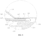
FIG. 5 is an enlarged regional schematic diagram of part B ofFIG. 4 . - 100-metal rear shell, 110-rear shell main body, 120-rear shell edge part, 200-rim structure, 210-rim main body, 220-positioning slot, 300-diffusion panel, 400-electromagnetic film, 410-film main body, 420-film edge part, 500-permanent magnet structure, 510-permanent magnet main body, 520-permanent magnet connecting part, 530-permanent magnet auxiliary body, 600-display screen body.
- Embodiments of the present invention are described in detail below, and examples of the embodiments are shown in the drawings, where same labels in respective drawings represent same parts. The embodiments described below with reference to the drawings are illustrative and are used only to explain the present invention and should not be understood as limitation to the present invention.
- As shown in
FIGS. 1 and 2 , embodiments of the invention provides an electromagnetic touch structure, including a frame structure and an electromagnetic screen structure disposed on the frame structure. The frame structure can provide support and fixation for the electromagnetic screen structure, and the electromagnetic screen structure can realize electromagnetic writing and control functions. - In particular, as shown in
FIG. 3 , the above-referenced frame structure includes a groove-shaped metal rear shell 100 (that is, the metalrear shell 100 protrudes outward) and arim structure 200 disposed at a peripheral edge of the metalrear shell 100. An edge of the electromagnetic screen structure is disposed on the metalrear shell 100, a middle part of the electromagnetic screen structure corresponds to a groove in the middle of the metal rear shell, and therim structure 200 provides peripheral positioning and fixing of the electromagnetic screen structure, so that the electromagnetic screen structure is fixed on the frame structure. Further, the metalrear shell 100 includes a groove-shaped rear shellmain body 110, and a rearshell edge part 120 disposed on a periphery of the rear shell main body, and the peripheral edge of the electromagnetic screen structure is disposed on the rearshell edge part 120, and the middle part of the electromagnetic screen structure is suspended above the rear shellmain body 110. In addition, therim structure 200 includes a rimmain body 210 disposed on the rearshell edge part 120, and apositioning slot 220 disposed on the rimmain body 210. Thepositioning slot 220 is located between the rimmain body 210 and the rearshell edge part 120, while the peripheral edge of the electromagnetic screen structure is located in thepositioning slot 220, thereby realizing the positioning and fixing of the electromagnetic screen structure. - Moreover, the electromagnetic screen structure includes a
diffusion panel 300 and anelectromagnetic film 400 which are stacked between the metalrear shell 100 and therim structure 200. Theelectromagnetic film 400 may be disposed above the diffusion panel 300 (that is, on a side of the diffusion panel away from the metal rear shell 100) or below the diffusion panel 300 (that is, on a side of the diffusion panel facing the metal rear shell 100). Moreover, surrounding edges of thediffusion panel 300 and theelectromagnetic film 400 are disposed in thepositioning slot 220 between the metalrear shell 100 and therim structure 200 to realize the fixation of thediffusion panel 300 and theelectromagnetic film 400. - In addition, the electromagnetic screen structure also includes a
permanent magnet structure 500 disposed at a peripheral edge of theelectromagnetic film 400, and thepermanent magnet structure 500 is located between the metalrear shell 100 and therim structure 200. In a traditional technical solution, because the peripheral edges of theelectromagnetic film 400 and the electromagnetic screen structure are disposed between the metalrear shell 100 and therim structure 200, a distance between the electromagnetic antenna module corresponding to theelectromagnetic film 400 and the metalrear shell 100 is relatively close. As a result, the metalrear shell 100 and therim structure 200 form an electromagnetic shielding to the edge part of the electromagnetic screen structure located between them, resulting in reduced magnetic flux of an electromagnetic coil of the electromagnetic antenna module at an edge position of themetal back case 100. In the present, by setting apermanent magnet structure 500 at the edge part of the electromagnetic screen structure, the magnetic flux of some coils of the electromagnetic antenna module corresponding to the edge position of the electromagnetic screen structure can be strengthened, thereby reducing or eliminating the electromagnetic signal shielding by the metalrear shell 100 and therim structure 200 to theelectromagnetic film 400 and the electromagnetic screen structure, and thus enabling the electromagnetic signal to be properly identified even at the edge position of the electromagnetic screen structure when electromagnetic writing is performed by using the electromagnetic screen structure, and ensuring normal use of the electromagnetic screen structure. - Further, the
electromagnetic film 400 includes a filmmain body 410 suspended above the rear shellmain body 110, and afilm edge part 420 disposed on a periphery of the filmmain body 410 and corresponding to the rearshell edge part 120. Thepermanent magnet structure 500 is disposed between thefilm edge part 420 and the rearshell edge part 120, and thefilm edge part 420 is also located in thepositioning slot 220 between the rearshell edge part 120 and the rimmain body 210. That is, the electromagnetic capacity of thefilm edge part 420 of theelectromagnetic film 400 located between the rearshell edge part 120 and the rimmain body 210 can be enhanced by thepermanent magnet structure 500, and the magnetic flux of some coils of the electromagnetic antenna module at thefilm edge part 420 can be strengthened, and the electromagnetic signal shielding of the metalrear shell 100 and therim structure 200 to thefilm edge part 420 can be reduced or eliminated, so that thefilm edge part 420 can also identify an electromagnetic signal properly, and thus, the wholeelectromagnetic film 400 can identify the electromagnetic signal properly, thereby ensuring normal operation of the whole electromagnetic touch structure. - Furthermore, as shown in
FIGS. 2 and3 , in some embodiments, thepermanent magnet structure 500 includes a permanent magnetmain body 510 disposed between thefilm edge part 420 and the rearshell edge part 120, and further incudes a permanentmagnet connecting part 520 connected to the permanent magnetmain body 510 and extended to an interior of the rear shell main body 110 (that is a side facing the diffusion panel 300). Setting the permanentmagnet connecting part 520 facilitates positioning and fixation of the entirepermanent magnet structure 500. Setting the permanent magnetmain body 510 located at thefilm edge part 420 facilitates enhancement of the electromagnetic performance of thefilm edge part 420. Moreover, the permanentmain body 510 is partially extended to the filmmain body 410, ensuring the electromagnetic performance of the connection transition between the filmmain body 410 and thefilm edge part 420. In addition, in this case, theelectromagnetic film 400 may be disposed under thediffusion panel 300, that is, theelectromagnetic film 400 is disposed on a side facing the metalrear shell 100. - In addition, as shown in
FIGS. 4 to 5 , in some other embodiments, thepermanent magnet structure 500 includes not only the permanent magnetmain body 510 disposed between thefilm edge part 420 and the rearshell edge part 120, but also a permanent magnetauxiliary body 530 located between thefilm edge part 420 and therim structure 200, and the permanent magnetmain body 510 and the permanent magnetauxiliary body 530 are respectively wrapped on both sides of thefilm edge part 420. By setting apermanent magnet structure 500 on both sides of thefilm edge part 420, the electromagnetic capacity of thefilm edge part 420 can be enhanced from both sides, so that thefilm edge part 420 can better identify the electromagnetic signal. Furthermore, the permanent magnetmain body 510 and the permanent magnetauxiliary body 530 both partially extend to the filmmain body 410, ensuring the electromagnetic performance of the connection transition between the filmmain body 410 and thefilm edge part 420. In addition, in this case, theelectromagnetic film 400 may be disposed below or above thediffusion panel 300. Moreover, the permanent magnetmain body 510 and the permanent magnetauxiliary body 530 may be disposed in a mutually independent manner, that is, they are respectively disposed on both sides of thefilm edge part 420; or, the permanent magnetmain body 510 may be extended around an end of thefilm edge part 420 and connected to the permanent magnetauxiliary body 530, that is, thepermanent magnet structure 500 may be set into a U-shaped structure to wrap on both sides of thefilm edge part 420. - In addition, the
permanent magnet structure 500 may be provided as silicon steel sheets, which have excellent electromagnetic capability and can significantly enhance the electromagnetic performance at the edge position of theelectromagnetic film 400. Moreover, thepermanent magnet structure 500 may be set as an integral structure, that is, an integral frame structure designed according to the peripheral edge shapes of the metalrear shell 100 and therim structure 200. In addition, thepermanent magnet structure 500 may also be set as a split structure, that is, thepermanent magnet structure 500 may be set as multiple silicon steel sheets, which are respectively disposed at the peripheral edges of the metalrear shell 100 and therim structure 200. - In addition, the electromagnetic touch structure also includes a reflector disposed inside the metal
rear shell 100 and corresponding to thediffusion panel 300, and thepermanent magnet structure 500 is disposed between the metalrear shell 100 and the reflector. In this way, thepermanent magnet structure 500 will not affect the optical performance of the electromagnetic touch structure. - In addition, the electromagnetic screen structure may also include a
display screen body 600 disposed in therim structure 200, where thedisplay screen body 600 corresponds to theelectromagnetic film 400. By setting thedisplay screen body 600, the electromagnetic screen structure can realize not only the electromagnetic touch function, but also the display function. In addition, in the present embodiment, therim structure 200 may be made of a metal material or a plastic material, or other materials as needed. - In addition, the present invention also provides a direct-backlight display module, which includes the electromagnetic touch structure as described above. In addition, the present invention also provides a display, which includes the direct-backlight display module as described above. In this way, by adding permanent magnet structures (such as silicon steel sheets) at the peripheral edge of the electromagnetic touch structure, the magnetic flux of edge part coils of the electromagnetic antenna module located at the edge of the metal rear shell is enhanced, so that the signal response to electromagnetic writing at the edge is improved in the application scenario, and the problem of abnormality in writing at the edge is improved, and thus the writing and touch functions of the electromagnetic touch structure can be normally used at the edge of the display.
- In addition, it should be understood that in the embodiments, the terms "lower", "upper", "front", "rear", "left", "right", "inside", "outside", "top", "bottom", "one side", "the other side", "one end", "the other end", etc., are based on the position relationship shown in the accompanying drawings; the terms "first" and "second" are used to distinguish different structural components. These terms are only intended to facilitate describing the present invention and simplifying the description, and should not be understood as limitations to the invention.
- The technical features of the above-mentioned embodiments may be combined arbitrarily. In order to make the description concise, all possible combinations of the various technical features in the embodiments are not described. However, as long as there is no contradiction between the combinations of these technical features, they should be considered as within the scope recorded in this specification.
- The above-mentioned embodiments only express several embodiments of the present invention, and their descriptions are specific and detailed, but they cannot be understood as a limitation on the scope of the present invention. It should be pointed out that, for ordinary technicians in the art, various deformations and improvements can be made without departing from the concept of the present invention, which all belong to the scope of protection of the present invention. Therefore, the scope of protection of the patent for the invention shall be based on the attached claims.
Claims (10)
- An electromagnetic touch structure, comprising a frame structure, and an electromagnetic screen structure disposed on the frame structure;
the frame structure comprising a groove-shaped metal rear shell and a rim structure circumferentially disposed at a peripheral edge of the metal rear shell;
the electromagnetic screen structure comprising a diffusion panel and an electromagnetic film which are stacked between the metal rear shell and the rim structure, and a permanent magnet structure disposed at a peripheral edge of the electromagnetic film, the permanent magnet structure being located between the metal rear shell and the rim structure, and the electromagnetic film being disposed above or below the diffusion panel. - The electromagnetic touch structure according to claim 1, wherein the permanent magnet structure is provided as silicon steel sheets.
- The electromagnetic touch structure according to claim 1, wherein the metal rear shell comprises a groove-shaped rear shell main body and a rear shell edge part disposed on a periphery of the rear shell main body, and
the electromagnetic film comprises a film main body suspended above the rear shell main body, and a film edge part disposed on a periphery of the film main body and corresponding to the rear shell edge part, and the permanent magnet structure is disposed between the film edge part and the rear shell edge part. - The electromagnetic touch structure according to claim 3, wherein the permanent magnet structure comprises a permanent magnet main body disposed between the film edge part and the rear shell edge part, and further comprises a permanent magnet connecting part connected to the permanent magnet main body and extended to an interior of the rear shell main body.
- The electromagnetic touch structure according to claim 3 or claim 4, wherein the permanent magnet structure comprises a permanent magnet main body disposed between the film edge part and the rear shell edge part, and further comprises a permanent magnet auxiliary body located between the film edge part and the rim structure, and the permanent magnet main body and the permanent magnet auxiliary body are respectively wrapped on two sides of the film edge part.
- The electromagnetic touch structure according to claim 5, wherein the permanent magnet main body and the permanent magnet auxiliary body are disposed in a mutually independent manner;
or, the permanent magnet main body is extended around an end of the film edge part and is connected to the permanent magnet auxiliary body. - The electromagnetic touch structure according to any one of claims 1 to 3, wherein the electromagnetic touch structure further comprises a reflector disposed inside the metal rear shell and corresponding to the diffusion panel, and the permanent magnet structure is disposed between the metal rear shell and the reflector.
- The electromagnetic touch structure according to any one of claims 1 to 3, wherein the electromagnetic screen structure further comprises a display screen body disposed in the rim structure, and the display screen body corresponds to the electromagnetic film.
- A direct-backlight display module, comprising the electromagnetic touch structure according to any one of claims 1 to 8.
- A display, comprising the direct-backlight display module according to claim 9.
Applications Claiming Priority (2)
| Application Number | Priority Date | Filing Date | Title |
|---|---|---|---|
| CN201820927188.8U CN208367670U (en) | 2018-06-14 | 2018-06-14 | Electromagnetic touch structure, direct type backlight display module and display |
| PCT/CN2018/118461 WO2019237669A1 (en) | 2018-06-14 | 2018-11-30 | Electromagnetic touch-control structure, direct-type backlight display module and display |
Publications (4)
| Publication Number | Publication Date |
|---|---|
| EP3809246A1 true EP3809246A1 (en) | 2021-04-21 |
| EP3809246A4 EP3809246A4 (en) | 2021-08-11 |
| EP3809246B1 EP3809246B1 (en) | 2024-04-24 |
| EP3809246B8 EP3809246B8 (en) | 2024-06-12 |
Family
ID=64929165
Family Applications (1)
| Application Number | Title | Priority Date | Filing Date |
|---|---|---|---|
| EP18922542.8A Active EP3809246B8 (en) | 2018-06-14 | 2018-11-30 | Electromagnetic touch-control structure, direct-type backlight display module and display |
Country Status (6)
| Country | Link |
|---|---|
| US (1) | US11188184B2 (en) |
| EP (1) | EP3809246B8 (en) |
| JP (1) | JP7278310B2 (en) |
| CN (1) | CN208367670U (en) |
| ES (1) | ES2983764T3 (en) |
| WO (1) | WO2019237669A1 (en) |
Families Citing this family (3)
| Publication number | Priority date | Publication date | Assignee | Title |
|---|---|---|---|---|
| CN209728723U (en) * | 2018-07-26 | 2019-12-03 | 广州视源电子科技股份有限公司 | Electromagnetic touch screen and interactive intelligent equipment |
| CN110517585A (en) * | 2019-09-26 | 2019-11-29 | 京东方科技集团股份有限公司 | Support construction for backlight module and the backlight module with it |
| CN118012292A (en) * | 2024-03-22 | 2024-05-10 | 深圳市弘扬德教科技有限公司 | Handwriting device with printing function |
Family Cites Families (14)
| Publication number | Priority date | Publication date | Assignee | Title |
|---|---|---|---|---|
| JPH0713144A (en) * | 1993-06-24 | 1995-01-17 | Canon Inc | Liquid crystal display |
| JPH07104935A (en) * | 1993-10-01 | 1995-04-21 | Totoku Electric Co Ltd | Liquid crystal display device having digitizer sensor section |
| US6215476B1 (en) * | 1997-10-10 | 2001-04-10 | Apple Computer, Inc. | Flat panel display with integrated electromagnetic pen digitizer |
| JP4126610B2 (en) * | 2002-12-26 | 2008-07-30 | エルジー ディスプレイ カンパニー リミテッド | Liquid crystal display |
| JP4177142B2 (en) * | 2003-03-10 | 2008-11-05 | 富士通コンポーネント株式会社 | Coordinate input device and drive device |
| JP5270482B2 (en) * | 2009-07-13 | 2013-08-21 | 株式会社ワコム | Position detecting device and sensor unit |
| KR101975596B1 (en) * | 2012-08-29 | 2019-05-07 | 삼성전자주식회사 | Touch screen device for compensating distortion of input sensing signal |
| US20170277282A1 (en) * | 2012-09-14 | 2017-09-28 | Widevantage Inc. | Input device for transmitting user input |
| US9489049B2 (en) * | 2014-08-26 | 2016-11-08 | Samsung Electronics Co., Ltd. | Force simulation finger sleeve using orthogonal uniform magnetic field |
| US9696752B2 (en) * | 2015-03-27 | 2017-07-04 | Apple Inc. | Dynamically stabilized magnetic array |
| US10437359B1 (en) * | 2017-02-28 | 2019-10-08 | Apple Inc. | Stylus with external magnetic influence |
| CN106980207B (en) * | 2017-05-12 | 2023-09-01 | 广州视源电子科技股份有限公司 | Direct-lit backlight display module and display device |
| CN207008591U (en) * | 2017-07-25 | 2018-02-13 | 朱智 | Backlight module and display device |
| US10656771B2 (en) * | 2018-02-27 | 2020-05-19 | Dell Products, Lp | Method and apparatus for multi configuration tuning for magnet to electromagnetic resonance panel proximity |
-
2018
- 2018-06-14 CN CN201820927188.8U patent/CN208367670U/en active Active
- 2018-11-30 JP JP2020568670A patent/JP7278310B2/en active Active
- 2018-11-30 WO PCT/CN2018/118461 patent/WO2019237669A1/en not_active Ceased
- 2018-11-30 ES ES18922542T patent/ES2983764T3/en active Active
- 2018-11-30 EP EP18922542.8A patent/EP3809246B8/en active Active
-
2020
- 2020-12-10 US US17/118,333 patent/US11188184B2/en active Active
Also Published As
| Publication number | Publication date |
|---|---|
| JP2021526273A (en) | 2021-09-30 |
| ES2983764T3 (en) | 2024-10-24 |
| JP7278310B2 (en) | 2023-05-19 |
| US11188184B2 (en) | 2021-11-30 |
| EP3809246B1 (en) | 2024-04-24 |
| US20210096673A1 (en) | 2021-04-01 |
| EP3809246A4 (en) | 2021-08-11 |
| EP3809246B8 (en) | 2024-06-12 |
| WO2019237669A1 (en) | 2019-12-19 |
| CN208367670U (en) | 2019-01-11 |
Similar Documents
| Publication | Publication Date | Title |
|---|---|---|
| US11188184B2 (en) | Electromagnetic touch structure, direct-backlight display module and display | |
| US20170346164A1 (en) | Electronic device with multi-slot antenna | |
| US11925010B2 (en) | Display panel, display module and manufacture method thereof, and communication device | |
| EP2487526A1 (en) | Display device | |
| US10355500B2 (en) | Wireless charging device | |
| US20200119438A1 (en) | Display device and communication system | |
| US20180035188A1 (en) | Electronic device with speaker | |
| CN214201993U (en) | Backlight module and display device | |
| CN108664176B (en) | Electromagnetic touch structure, lateral backlight display module and display | |
| US20200218308A1 (en) | Backlight Module and Display Device | |
| CN210804357U (en) | Touch screen with sound production function | |
| US20170371094A1 (en) | Backlight module and display device | |
| KR20130105973A (en) | Mobile terminal | |
| CN113056857B (en) | Wireless Charging Coil Assembly | |
| CN208367671U (en) | Electromagnetic touch structure, lateral backlight display module and display | |
| KR20130105082A (en) | Mobile terminal | |
| CN209057448U (en) | A kind of vehicle electronic device | |
| CN217181373U (en) | Display module and display device | |
| JP4201637B2 (en) | Flat speaker and electronic device using the same | |
| JP7295625B2 (en) | Position detection unit | |
| CN207571988U (en) | Antifalsification label card and packing case | |
| JP4211160B2 (en) | speaker | |
| EP3483775A1 (en) | Display module and display device with near field communication module | |
| KR20150008998A (en) | Mobile terminal | |
| US11868838B2 (en) | Device supporting card-swiping |
Legal Events
| Date | Code | Title | Description |
|---|---|---|---|
| STAA | Information on the status of an ep patent application or granted ep patent |
Free format text: STATUS: THE INTERNATIONAL PUBLICATION HAS BEEN MADE |
|
| PUAI | Public reference made under article 153(3) epc to a published international application that has entered the european phase |
Free format text: ORIGINAL CODE: 0009012 |
|
| STAA | Information on the status of an ep patent application or granted ep patent |
Free format text: STATUS: REQUEST FOR EXAMINATION WAS MADE |
|
| 17P | Request for examination filed |
Effective date: 20210112 |
|
| AK | Designated contracting states |
Kind code of ref document: A1 Designated state(s): AL AT BE BG CH CY CZ DE DK EE ES FI FR GB GR HR HU IE IS IT LI LT LU LV MC MK MT NL NO PL PT RO RS SE SI SK SM TR |
|
| AX | Request for extension of the european patent |
Extension state: BA ME |
|
| A4 | Supplementary search report drawn up and despatched |
Effective date: 20210713 |
|
| RIC1 | Information provided on ipc code assigned before grant |
Ipc: G06F 3/041 20060101ALI20210707BHEP Ipc: G06F 3/046 20060101AFI20210707BHEP |
|
| DAV | Request for validation of the european patent (deleted) | ||
| DAX | Request for extension of the european patent (deleted) | ||
| GRAP | Despatch of communication of intention to grant a patent |
Free format text: ORIGINAL CODE: EPIDOSNIGR1 |
|
| STAA | Information on the status of an ep patent application or granted ep patent |
Free format text: STATUS: GRANT OF PATENT IS INTENDED |
|
| INTG | Intention to grant announced |
Effective date: 20230912 |
|
| P01 | Opt-out of the competence of the unified patent court (upc) registered |
Effective date: 20231116 |
|
| GRAS | Grant fee paid |
Free format text: ORIGINAL CODE: EPIDOSNIGR3 |
|
| RAP3 | Party data changed (applicant data changed or rights of an application transferred) |
Owner name: GUANGZHOU SHIRUI ELECTRONICS CO., LTD. Owner name: GUANGZHOU SHIYUAN ELECTRONICS CO., LTD. |
|
| GRAA | (expected) grant |
Free format text: ORIGINAL CODE: 0009210 |
|
| STAA | Information on the status of an ep patent application or granted ep patent |
Free format text: STATUS: THE PATENT HAS BEEN GRANTED |
|
| GRAT | Correction requested after decision to grant or after decision to maintain patent in amended form |
Free format text: ORIGINAL CODE: EPIDOSNCDEC |
|
| RAP3 | Party data changed (applicant data changed or rights of an application transferred) |
Owner name: GUANGZHOU SHIRUI ELECTRONICS CO., LTD. Owner name: GUANGZHOU SHIYUAN ELECTRONIC TECHNOLOGY COMPANY LIMITED |
|
| AK | Designated contracting states |
Kind code of ref document: B1 Designated state(s): AL AT BE BG CH CY CZ DE DK EE ES FI FR GB GR HR HU IE IS IT LI LT LU LV MC MK MT NL NO PL PT RO RS SE SI SK SM TR |
|
| REG | Reference to a national code |
Ref country code: GB Ref legal event code: FG4D |
|
| REG | Reference to a national code |
Ref country code: CH Ref legal event code: EP |
|
| RAP4 | Party data changed (patent owner data changed or rights of a patent transferred) |
Owner name: GUANGZHOU SHIRUI ELECTRONICS CO., LTD. Owner name: GUANGZHOU SHIYUAN ELECTRONIC TECHNOLOGY COMPANY LIMITED |
|
| REG | Reference to a national code |
Ref country code: CH Ref legal event code: PK Free format text: BERICHTIGUNG B8 |
|
| REG | Reference to a national code |
Ref country code: DE Ref legal event code: R096 Ref document number: 602018068731 Country of ref document: DE |
|
| REG | Reference to a national code |
Ref country code: IE Ref legal event code: FG4D |
|
| REG | Reference to a national code |
Ref country code: NL Ref legal event code: FP |
|
| REG | Reference to a national code |
Ref country code: LT Ref legal event code: MG9D |
|
| REG | Reference to a national code |
Ref country code: AT Ref legal event code: MK05 Ref document number: 1680317 Country of ref document: AT Kind code of ref document: T Effective date: 20240424 |
|
| PG25 | Lapsed in a contracting state [announced via postgrant information from national office to epo] |
Ref country code: IS Free format text: LAPSE BECAUSE OF FAILURE TO SUBMIT A TRANSLATION OF THE DESCRIPTION OR TO PAY THE FEE WITHIN THE PRESCRIBED TIME-LIMIT Effective date: 20240824 |
|
| PG25 | Lapsed in a contracting state [announced via postgrant information from national office to epo] |
Ref country code: BG Free format text: LAPSE BECAUSE OF FAILURE TO SUBMIT A TRANSLATION OF THE DESCRIPTION OR TO PAY THE FEE WITHIN THE PRESCRIBED TIME-LIMIT Effective date: 20240424 |
|
| PG25 | Lapsed in a contracting state [announced via postgrant information from national office to epo] |
Ref country code: FI Free format text: LAPSE BECAUSE OF FAILURE TO SUBMIT A TRANSLATION OF THE DESCRIPTION OR TO PAY THE FEE WITHIN THE PRESCRIBED TIME-LIMIT Effective date: 20240424 Ref country code: HR Free format text: LAPSE BECAUSE OF FAILURE TO SUBMIT A TRANSLATION OF THE DESCRIPTION OR TO PAY THE FEE WITHIN THE PRESCRIBED TIME-LIMIT Effective date: 20240424 |
|
| PG25 | Lapsed in a contracting state [announced via postgrant information from national office to epo] |
Ref country code: GR Free format text: LAPSE BECAUSE OF FAILURE TO SUBMIT A TRANSLATION OF THE DESCRIPTION OR TO PAY THE FEE WITHIN THE PRESCRIBED TIME-LIMIT Effective date: 20240725 |
|
| PG25 | Lapsed in a contracting state [announced via postgrant information from national office to epo] |
Ref country code: PT Free format text: LAPSE BECAUSE OF FAILURE TO SUBMIT A TRANSLATION OF THE DESCRIPTION OR TO PAY THE FEE WITHIN THE PRESCRIBED TIME-LIMIT Effective date: 20240826 |
|
| PG25 | Lapsed in a contracting state [announced via postgrant information from national office to epo] |
Ref country code: AT Free format text: LAPSE BECAUSE OF FAILURE TO SUBMIT A TRANSLATION OF THE DESCRIPTION OR TO PAY THE FEE WITHIN THE PRESCRIBED TIME-LIMIT Effective date: 20240424 |
|
| REG | Reference to a national code |
Ref country code: ES Ref legal event code: FG2A Ref document number: 2983764 Country of ref document: ES Kind code of ref document: T3 Effective date: 20241024 |
|
| PG25 | Lapsed in a contracting state [announced via postgrant information from national office to epo] |
Ref country code: PL Free format text: LAPSE BECAUSE OF FAILURE TO SUBMIT A TRANSLATION OF THE DESCRIPTION OR TO PAY THE FEE WITHIN THE PRESCRIBED TIME-LIMIT Effective date: 20240424 |
|
| PG25 | Lapsed in a contracting state [announced via postgrant information from national office to epo] |
Ref country code: LV Free format text: LAPSE BECAUSE OF FAILURE TO SUBMIT A TRANSLATION OF THE DESCRIPTION OR TO PAY THE FEE WITHIN THE PRESCRIBED TIME-LIMIT Effective date: 20240424 |
|
| PG25 | Lapsed in a contracting state [announced via postgrant information from national office to epo] |
Ref country code: PT Free format text: LAPSE BECAUSE OF FAILURE TO SUBMIT A TRANSLATION OF THE DESCRIPTION OR TO PAY THE FEE WITHIN THE PRESCRIBED TIME-LIMIT Effective date: 20240826 Ref country code: PL Free format text: LAPSE BECAUSE OF FAILURE TO SUBMIT A TRANSLATION OF THE DESCRIPTION OR TO PAY THE FEE WITHIN THE PRESCRIBED TIME-LIMIT Effective date: 20240424 Ref country code: NO Free format text: LAPSE BECAUSE OF FAILURE TO SUBMIT A TRANSLATION OF THE DESCRIPTION OR TO PAY THE FEE WITHIN THE PRESCRIBED TIME-LIMIT Effective date: 20240724 Ref country code: LV Free format text: LAPSE BECAUSE OF FAILURE TO SUBMIT A TRANSLATION OF THE DESCRIPTION OR TO PAY THE FEE WITHIN THE PRESCRIBED TIME-LIMIT Effective date: 20240424 Ref country code: IS Free format text: LAPSE BECAUSE OF FAILURE TO SUBMIT A TRANSLATION OF THE DESCRIPTION OR TO PAY THE FEE WITHIN THE PRESCRIBED TIME-LIMIT Effective date: 20240824 Ref country code: HR Free format text: LAPSE BECAUSE OF FAILURE TO SUBMIT A TRANSLATION OF THE DESCRIPTION OR TO PAY THE FEE WITHIN THE PRESCRIBED TIME-LIMIT Effective date: 20240424 Ref country code: GR Free format text: LAPSE BECAUSE OF FAILURE TO SUBMIT A TRANSLATION OF THE DESCRIPTION OR TO PAY THE FEE WITHIN THE PRESCRIBED TIME-LIMIT Effective date: 20240725 Ref country code: FI Free format text: LAPSE BECAUSE OF FAILURE TO SUBMIT A TRANSLATION OF THE DESCRIPTION OR TO PAY THE FEE WITHIN THE PRESCRIBED TIME-LIMIT Effective date: 20240424 Ref country code: BG Free format text: LAPSE BECAUSE OF FAILURE TO SUBMIT A TRANSLATION OF THE DESCRIPTION OR TO PAY THE FEE WITHIN THE PRESCRIBED TIME-LIMIT Effective date: 20240424 Ref country code: AT Free format text: LAPSE BECAUSE OF FAILURE TO SUBMIT A TRANSLATION OF THE DESCRIPTION OR TO PAY THE FEE WITHIN THE PRESCRIBED TIME-LIMIT Effective date: 20240424 Ref country code: RS Free format text: LAPSE BECAUSE OF FAILURE TO SUBMIT A TRANSLATION OF THE DESCRIPTION OR TO PAY THE FEE WITHIN THE PRESCRIBED TIME-LIMIT Effective date: 20240724 |
|
| PG25 | Lapsed in a contracting state [announced via postgrant information from national office to epo] |
Ref country code: DK Free format text: LAPSE BECAUSE OF FAILURE TO SUBMIT A TRANSLATION OF THE DESCRIPTION OR TO PAY THE FEE WITHIN THE PRESCRIBED TIME-LIMIT Effective date: 20240424 |
|
| PG25 | Lapsed in a contracting state [announced via postgrant information from national office to epo] |
Ref country code: EE Free format text: LAPSE BECAUSE OF FAILURE TO SUBMIT A TRANSLATION OF THE DESCRIPTION OR TO PAY THE FEE WITHIN THE PRESCRIBED TIME-LIMIT Effective date: 20240424 |
|
| PG25 | Lapsed in a contracting state [announced via postgrant information from national office to epo] |
Ref country code: CZ Free format text: LAPSE BECAUSE OF FAILURE TO SUBMIT A TRANSLATION OF THE DESCRIPTION OR TO PAY THE FEE WITHIN THE PRESCRIBED TIME-LIMIT Effective date: 20240424 |
|
| PG25 | Lapsed in a contracting state [announced via postgrant information from national office to epo] |
Ref country code: SK Free format text: LAPSE BECAUSE OF FAILURE TO SUBMIT A TRANSLATION OF THE DESCRIPTION OR TO PAY THE FEE WITHIN THE PRESCRIBED TIME-LIMIT Effective date: 20240424 Ref country code: RO Free format text: LAPSE BECAUSE OF FAILURE TO SUBMIT A TRANSLATION OF THE DESCRIPTION OR TO PAY THE FEE WITHIN THE PRESCRIBED TIME-LIMIT Effective date: 20240424 |
|
| REG | Reference to a national code |
Ref country code: DE Ref legal event code: R097 Ref document number: 602018068731 Country of ref document: DE |
|
| PG25 | Lapsed in a contracting state [announced via postgrant information from national office to epo] |
Ref country code: SM Free format text: LAPSE BECAUSE OF FAILURE TO SUBMIT A TRANSLATION OF THE DESCRIPTION OR TO PAY THE FEE WITHIN THE PRESCRIBED TIME-LIMIT Effective date: 20240424 |
|
| PG25 | Lapsed in a contracting state [announced via postgrant information from national office to epo] |
Ref country code: SM Free format text: LAPSE BECAUSE OF FAILURE TO SUBMIT A TRANSLATION OF THE DESCRIPTION OR TO PAY THE FEE WITHIN THE PRESCRIBED TIME-LIMIT Effective date: 20240424 Ref country code: SK Free format text: LAPSE BECAUSE OF FAILURE TO SUBMIT A TRANSLATION OF THE DESCRIPTION OR TO PAY THE FEE WITHIN THE PRESCRIBED TIME-LIMIT Effective date: 20240424 Ref country code: RO Free format text: LAPSE BECAUSE OF FAILURE TO SUBMIT A TRANSLATION OF THE DESCRIPTION OR TO PAY THE FEE WITHIN THE PRESCRIBED TIME-LIMIT Effective date: 20240424 Ref country code: EE Free format text: LAPSE BECAUSE OF FAILURE TO SUBMIT A TRANSLATION OF THE DESCRIPTION OR TO PAY THE FEE WITHIN THE PRESCRIBED TIME-LIMIT Effective date: 20240424 Ref country code: DK Free format text: LAPSE BECAUSE OF FAILURE TO SUBMIT A TRANSLATION OF THE DESCRIPTION OR TO PAY THE FEE WITHIN THE PRESCRIBED TIME-LIMIT Effective date: 20240424 Ref country code: CZ Free format text: LAPSE BECAUSE OF FAILURE TO SUBMIT A TRANSLATION OF THE DESCRIPTION OR TO PAY THE FEE WITHIN THE PRESCRIBED TIME-LIMIT Effective date: 20240424 |
|
| PLBE | No opposition filed within time limit |
Free format text: ORIGINAL CODE: 0009261 |
|
| STAA | Information on the status of an ep patent application or granted ep patent |
Free format text: STATUS: NO OPPOSITION FILED WITHIN TIME LIMIT |
|
| 26N | No opposition filed |
Effective date: 20250127 |
|
| PG25 | Lapsed in a contracting state [announced via postgrant information from national office to epo] |
Ref country code: SI Free format text: LAPSE BECAUSE OF FAILURE TO SUBMIT A TRANSLATION OF THE DESCRIPTION OR TO PAY THE FEE WITHIN THE PRESCRIBED TIME-LIMIT Effective date: 20240424 |
|
| REG | Reference to a national code |
Ref country code: CH Ref legal event code: PL |
|
| PG25 | Lapsed in a contracting state [announced via postgrant information from national office to epo] |
Ref country code: MC Free format text: LAPSE BECAUSE OF FAILURE TO SUBMIT A TRANSLATION OF THE DESCRIPTION OR TO PAY THE FEE WITHIN THE PRESCRIBED TIME-LIMIT Effective date: 20240424 |
|
| PG25 | Lapsed in a contracting state [announced via postgrant information from national office to epo] |
Ref country code: LU Free format text: LAPSE BECAUSE OF NON-PAYMENT OF DUE FEES Effective date: 20241130 |
|
| REG | Reference to a national code |
Ref country code: CH Ref legal event code: PL |
|
| PG25 | Lapsed in a contracting state [announced via postgrant information from national office to epo] |
Ref country code: CH Free format text: LAPSE BECAUSE OF NON-PAYMENT OF DUE FEES Effective date: 20241130 |
|
| REG | Reference to a national code |
Ref country code: BE Ref legal event code: MM Effective date: 20241130 |
|
| PG25 | Lapsed in a contracting state [announced via postgrant information from national office to epo] |
Ref country code: SE Free format text: LAPSE BECAUSE OF FAILURE TO SUBMIT A TRANSLATION OF THE DESCRIPTION OR TO PAY THE FEE WITHIN THE PRESCRIBED TIME-LIMIT Effective date: 20240424 |
|
| PG25 | Lapsed in a contracting state [announced via postgrant information from national office to epo] |
Ref country code: BE Free format text: LAPSE BECAUSE OF NON-PAYMENT OF DUE FEES Effective date: 20241130 |
|
| PG25 | Lapsed in a contracting state [announced via postgrant information from national office to epo] |
Ref country code: IE Free format text: LAPSE BECAUSE OF NON-PAYMENT OF DUE FEES Effective date: 20241130 |
|
| PGFP | Annual fee paid to national office [announced via postgrant information from national office to epo] |
Ref country code: NL Payment date: 20251119 Year of fee payment: 8 |
|
| PGFP | Annual fee paid to national office [announced via postgrant information from national office to epo] |
Ref country code: DE Payment date: 20251119 Year of fee payment: 8 |
|
| PGFP | Annual fee paid to national office [announced via postgrant information from national office to epo] |
Ref country code: GB Payment date: 20251121 Year of fee payment: 8 |
|
| PGFP | Annual fee paid to national office [announced via postgrant information from national office to epo] |
Ref country code: FR Payment date: 20251126 Year of fee payment: 8 |
|
| PG25 | Lapsed in a contracting state [announced via postgrant information from national office to epo] |
Ref country code: IT Free format text: LAPSE BECAUSE OF FAILURE TO SUBMIT A TRANSLATION OF THE DESCRIPTION OR TO PAY THE FEE WITHIN THE PRESCRIBED TIME-LIMIT Effective date: 20240424 |
|
| PGFP | Annual fee paid to national office [announced via postgrant information from national office to epo] |
Ref country code: ES Payment date: 20251229 Year of fee payment: 8 |
|
| PG25 | Lapsed in a contracting state [announced via postgrant information from national office to epo] |
Ref country code: CY Free format text: LAPSE BECAUSE OF FAILURE TO SUBMIT A TRANSLATION OF THE DESCRIPTION OR TO PAY THE FEE WITHIN THE PRESCRIBED TIME-LIMIT; INVALID AB INITIO Effective date: 20181130 |