EP3806492B1 - Passive thermal-control system of a mesh network device and associated mesh network devices - Google Patents
Passive thermal-control system of a mesh network device and associated mesh network devices Download PDFInfo
- Publication number
- EP3806492B1 EP3806492B1 EP20200820.7A EP20200820A EP3806492B1 EP 3806492 B1 EP3806492 B1 EP 3806492B1 EP 20200820 A EP20200820 A EP 20200820A EP 3806492 B1 EP3806492 B1 EP 3806492B1
- Authority
- EP
- European Patent Office
- Prior art keywords
- heat
- integrated circuit
- heat sink
- mesh network
- network device
- Prior art date
- Legal status (The legal status is an assumption and is not a legal conclusion. Google has not performed a legal analysis and makes no representation as to the accuracy of the status listed.)
- Active
Links
Images



Classifications
-
- H—ELECTRICITY
- H05—ELECTRIC TECHNIQUES NOT OTHERWISE PROVIDED FOR
- H05K—PRINTED CIRCUITS; CASINGS OR CONSTRUCTIONAL DETAILS OF ELECTRIC APPARATUS; MANUFACTURE OF ASSEMBLAGES OF ELECTRICAL COMPONENTS
- H05K7/00—Constructional details common to different types of electric apparatus
- H05K7/20—Modifications to facilitate cooling, ventilating, or heating
- H05K7/2039—Modifications to facilitate cooling, ventilating, or heating characterised by the heat transfer by conduction from the heat generating element to a dissipating body
-
- H—ELECTRICITY
- H05—ELECTRIC TECHNIQUES NOT OTHERWISE PROVIDED FOR
- H05K—PRINTED CIRCUITS; CASINGS OR CONSTRUCTIONAL DETAILS OF ELECTRIC APPARATUS; MANUFACTURE OF ASSEMBLAGES OF ELECTRICAL COMPONENTS
- H05K7/00—Constructional details common to different types of electric apparatus
- H05K7/20—Modifications to facilitate cooling, ventilating, or heating
- H05K7/2039—Modifications to facilitate cooling, ventilating, or heating characterised by the heat transfer by conduction from the heat generating element to a dissipating body
- H05K7/20509—Multiple-component heat spreaders; Multi-component heat-conducting support plates; Multi-component non-closed heat-conducting structures
-
- H—ELECTRICITY
- H04—ELECTRIC COMMUNICATION TECHNIQUE
- H04R—LOUDSPEAKERS, MICROPHONES, GRAMOPHONE PICK-UPS OR LIKE ACOUSTIC ELECTROMECHANICAL TRANSDUCERS; ELECTRIC HEARING AIDS; PUBLIC ADDRESS SYSTEMS
- H04R9/00—Transducers of moving-coil, moving-strip, or moving-wire type
- H04R9/02—Details
- H04R9/022—Cooling arrangements
-
- H—ELECTRICITY
- H04—ELECTRIC COMMUNICATION TECHNIQUE
- H04R—LOUDSPEAKERS, MICROPHONES, GRAMOPHONE PICK-UPS OR LIKE ACOUSTIC ELECTROMECHANICAL TRANSDUCERS; ELECTRIC HEARING AIDS; PUBLIC ADDRESS SYSTEMS
- H04R9/00—Transducers of moving-coil, moving-strip, or moving-wire type
- H04R9/06—Loudspeakers
Definitions
- the present specification relates to embodiments of an apparatus including a speaker module and a passive thermal-control system.
- a mesh network is a network that includes multiple nodes that link together to improve network performance and network accessibility.
- a mesh network supporting a wireless local area network may include multiple wireless nodes linking together across an area.
- Each wireless node, or mesh network device may provide wireless devices access to the WLAN and exchange network information with other mesh network devices.
- the aggregate functions of the multiple mesh network devices in general, improve connectivity to the WLAN across the area and improve efficiency of data exchange.
- the mesh network device may be a range-extending mesh network device that includes a voice assistant.
- the mesh network device may be a small form-factor and include multiple electronic subsystems that generate heat.
- An example of an electronic subsystem is a printed circuit board (PCB) that is populated with a variety of integrated circuit (IC) devices.
- Another example of an electronic subsystem is a speaker module that may be used by the voice assistant.
- thermal-control system may be used.
- an active thermal-control system such as a thermal-control system that circulates a coolant or a liquid, may not be feasible due to form-factor and/or power consumption considerations.
- US 2015/382448 A1 relates to system-in-package assemblies in portable electronic devices.
- US 2019/104640 A1 relates to a mid-spreader for stacked circuit boards in an electronic device.
- the passive thermal-control system which may include a heat sink and multiple heat spreaders, is structured such that heat originating from IC devices of the mesh network device and a speaker module of the mesh network device may be transferred to other components of the mesh network device, such as a housing component. The heat may then be dissipated to an external environment to maintain a desired thermal profile of the mesh network device.
- Heat transfer in general, is energy that is in transit due to a temperature difference. If one or more temperature differences exist across components of a system, such as the mesh network device, heat (e.g., energy in Joules (J)) will transfer from higher temperature zones to lower temperature zones to reduce the temperature differences. There are several mechanisms for heat transfer across the components of the system to reduce temperature differences, including convection, radiation, and conduction.
- q conv represents a rate of heat transfer from a surface through convection (e . g ., in J per second or Watts (W))
- h represents a convection heat-transfer coefficient ( e . g ., in W per meter squared (W/m 2 ))
- T s represents a temperature of a surface ( e.g., in Kelvin (K) or degrees Celsius (°C))
- T ⁇ represents a temperature of a fluid ( e.g., in K or °C) to which the surface is exposed.
- A represents an area of a surface ( e . g ., in m 2 ).
- q rad represents a rate of heat transfer through radiation (e.g., in W)
- ⁇ represents emissivity (dimensionless)
- T s represents a temperature of a surface (e.g., in K or °C)
- T surr represents a temperature of surroundings of the surface ( e . g ., in K or °C).
- A represents an area of the surface ( e . g ., in m 2 ).
- q cond represents a rate of heat transfer in a solid material through conduction (e.g., in W)
- k represents a thermal conductivity of the solid material (e.g., in W/(m ⁇ K))
- dT / dx represents a temperature gradient through the solid material (e.g., in K/m or °C/m).
- A represents a cross-sectional area of the solid material (e.g., in m 2 ).
- the physical bodies may be in thermal contact. In some instances, this can include direct physical contact between the bodies or a material (e . g ., a TIM) located between the bodies, enabling conduction-based heat transfer between the bodies. In other instances, this can include an air gap between the bodies that enables convection-based and/or radiation-based heat transfer between the bodies.
- a material e . g ., a TIM
- a mesh network device includes a passive thermal-control system that, e.g., transfers heat using one or more of the heat-transfer mechanisms described above.
- rates and/or quantities of heat transfer can be varied by increasing or decreasing surface areas for convection and/or radiation within the mesh network device (e.g., increasing or decreasing surface areas of planar heat spreaders).
- rates and/or quantities of heat transfer can also be varied by introducing, between surfaces, one or more thermal interface materials (TIMs) that have a high thermal conductivity.
- TIMs thermal interface materials
- the passive thermal-control system may transfer heat originating from heat-generating electronic devices within the mesh network device to an interior surface of a housing component of the mesh network device.
- An exterior surface of the housing component may then dissipate the heat to an external environment through convection and/or radiation, effective to prevent degradation of the electronic subsystems that may include the heat-generating electronic devices.
- FIG. 1 illustrates an example operating environment 100 including a mesh network device 102.
- the mesh network device 102 includes multiple electronic devices, including a PCB 104 populated with one or more IC devices.
- the mesh network device 102 also includes a speaker module 106.
- the mesh network device 102 may serve as a node of a wireless mesh network (e.g., a WLAN network conforming to IEEE 802.11 communication protocols (Wi-Fi)).
- a wireless mesh network e.g., a WLAN network conforming to IEEE 802.11 communication protocols (Wi-Fi)
- the mesh network device 102 may wirelessly couple other wireless devices (e.g., a wireless phone, a laptop computer) to the wireless mesh network.
- the mesh network device 102 may, in some instances, include a voice-assistant to receive audible inputs from a user of the mesh network device 102.
- the mesh network device 102 may receive, through the speaker module 106 and from a user of the mesh network device 102, a vocal command that the mesh network device 102 transmits to one or more applications available through the wireless mesh network (e.g., available from a cloud-computing environment or available through another device to which the mesh network device 102 is wirelessly coupled).
- the vocal command may be transmitted to a remote application supporting a home automation or security system.
- the mesh network device 102 may receive, through the speaker module and from the user of the mesh network device 102, a vocal query.
- the mesh network device 102 may transmit the vocal query to one or more other applications available through the wireless mesh network (e.g., available from a cloud-computing environment or available through another device to which the mesh network device 102 is wirelessly coupled).
- the vocal query may direct a search to be performed by a search engine available through the wireless mesh network.
- the vocal query may direct media to be streamed through the speaker module 106 of the mesh network device 102 (e.g., play music through the mesh network device 102).
- the one or more IC devices populated on the PCB 104 and the speaker module 106 may generate an internal heat load 108 within the mesh network device 102.
- a passive thermal-control system 110 is used.
- the passive thermal-control system 110 includes multiple elements, including a heat sink 112, a heat-sink heat spreader 114, and a speaker-module heat spreader 116 (not visible in FIG. 1 ). In some instances, the passive thermal-control system 110 may also include multiple thermal interface materials (TIMs).
- TIMs thermal interface materials
- the heat sink 112 is generally cylindrical in shape, die-cast from a metal material (e.g., an aluminum material, a magnesium material).
- the heat-sink heat spreader 114 and the speaker-module heat spreader 116 each may be generally elliptical (or generally circular) in shape.
- the heat-sink heat spreader 114 and the speaker-module heat spreader 116 each are also generally planar, formed from respective sheets of a graphite material.
- the elements of the passive thermal-control system 110 conduct, spread, and transfer the internal heat load 108 (e.g., a rate of heat transfer q i in Watts) to a housing component 118 of the mesh network device 102 or to a base 120 of the mesh network device.
- the housing component(s) 118 may then dissipate the internal heat load 108 (e.g., using a thermal-convection heat-transfer mechanism and/or a thermal-radiation heat-transfer mechanism) to an external environment.
- portions of the internal heat load 108 transferred to the housing component(s) 118 may vary.
- the passive thermal-control system 110 further maintains a desired thermal profile of the mesh network device 102.
- the conduction, spreading, and transfer of the internal heat load 108 by the passive thermal-control system 110 may maintain a surface temperature of the housing component(s) 118 at or below a temperature of approximately 67° Celsius (°C) while the mesh network device 102 is operating in ambient conditions of 25 °C.
- the passive thermal-control system 110 may also maintain junction temperatures of the IC devices populating the PCB 104 at or below different respective temperature thresholds.
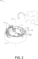
- FIG. 2 illustrates a top isometric view 200 of an example heat sink and an example heat-sink heat spreader (e.g., the heat sink 112 and the heat-sink heat spreader 114 of FIG. 1 ).
- the heat sink 112 includes a body 202 that is generally disk-like (e.g., middle region of the heat sink 112) extending radially from a central axis 204 to define a perimeter.
- the body 202 includes a first generally planar surface 206 (located under the heat-sink heat spreader 114 in FIG. 2 ) that is substantially orthogonal to the central axis 204.
- the heat-sink heat spreader 114 attaches to the first generally planar surface 206 ( e.g., using a thermally conductive epoxy). Further, the heat-sink heat spreader 114 may be positioned coaxially with the heat sink 112, according to the central axis 204.
- the heat-sink heat spreader 114 may spread and transfer heat to the body 202 using a thermal-conduction heat-transfer mechanism. In other instances, the heat-sink heat spreader 114 may spread and transfer heat to a surrounding environment ( e.g., a cavity within the mesh network device 102 of FIG. 1 ) using a thermal-convection heat-transfer mechanism and/or a thermal-radiation heat-transfer mechanism. For example, the heat-sink heat spreader 114 may spread and transfer heat in a generally outward direction away from the first generally planar surface 206 of the body 202 of the heat sink 112.
- the heat-sink heat spreader 114 may include one or more sheets (e.g., layers) of a thermally conductive material such as a graphite material. Furthermore, different types of materials may be selected to increase or decrease emissivity ( ⁇ ) and alter thermal radiation characteristics of the heat-sink heat spreader 114.
- the heat sink 112 may include one or more fin region(s) 208. Each fin region 208 may extend from the perimeter of the body 202 in one or more directions that are substantially parallel to the central axis 204. Furthermore, each fin region 208 may include an interior surface 210 and an opposing exterior surface 212. In some instances, each fin region 208 may transfer heat to a surrounding environment (e.g., to a cavity within the mesh network device 102 of FIG. 1 or to the housing component(s) 118 of the mesh network device of FIG. 1 ) using one or more of a thermal conduction, a thermal convection, and/or a thermal-radiation heat-transfer mechanism.
- the heat sink 112 may also include mounts, stands, or other fixturing mechanisms for one or more antenna(s) 214 that support wireless communications.
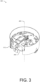
- FIG. 3 illustrates a bottom isometric view 300 of an example heat sink (e.g., the heat sink 112 of FIG. 1 ).
- the body 202 of the heat sink 112 includes a second generally planar surface (e.g., second generally planar surface 302 that is opposite the first generally planar surface 206 of FIG. 1 ).
- the second generally planar surface 302 may be generally orthogonal to the central axis 204.
- the second generally planar surface may face a speaker module (e.g., the speaker module 106).
- the body 202 includes one or more pedestal(s) 304 that protrude from the second generally planar surface 302.
- Each pedestal 304 may interface with a thermal interface material (TIM) and enable the TIM to make physical (and thermally conductive) contact with a respective, heat-generating device (e.g., an IC device that may be part of the PCB 104 of FIG. 1 ).
- the TIM may effectuate thermal coupling between the heat-generating device and the pedestal 304.
- the pedestal 304 may, in turn, and using a thermal-conduction heat-transfer mechanism, transfer heat to the body 202 of the heat sink 112.
- TIMs examples include gel materials and/or grease materials that may be thermally conductive. These materials may be injected with nano-particles, such as magnesium or aluminum nano-particles, to improve thermal conduction properties. Furthermore, TIMs located between the heat-generating devices and the one or more pedestal(s) 304 may reduce gaps and/or bond line gaps and improve thermal conduction efficiencies. Other examples of TIMs include thermally conductive foam materials and thermally conductive pad materials.
- FIG. 4 illustrates a top isometric view 400 of an example speaker-module subassembly 402 that may be included in a mesh network device ( e.g., the speaker-module subassembly 402 may be part of the speaker module 106 of the mesh network device 102 of FIG. 1 ).
- the speaker-module subassembly 402 includes a base 404 and a speaker-module driver 406.
- the base 404 includes an interior surface 408 that is generally planar and substantially orthogonal to the central axis 204.
- the interior surface 408 faces a second surface of a heat sink (e.g., the second generally planar surface 302).
- a heat spreader attaches to the interior surface 408 of the base 404.
- the speaker-module heat spreader 116 may attach to the interior surface 408 using a thermally conductive epoxy.
- the interior surface 408 may face a surface of a heat sink (e.g., the second generally planar surface 302 of FIG. 2 ).
- the speaker-module heat spreader 116 may be located between the interior surface 408 and a magnet of the speaker-module driver 406.
- the speaker-module heat spreader 116 may use a thermal-conduction heat-transfer mechanism to transfer heat from the speaker-module driver 406 to the base 404.
- the base 404 may use thermal conduction and/or thermal convection heat-transfer mechanisms to transfer the heat to a surrounding environment.
- the speaker-module heat spreader 116 may include one or more sheets (e.g., layers) of a thermally conductive material such as a graphite material. Furthermore, different types of materials may be selected to increase or decrease emissivity ( ⁇ ) and alter thermal radiation characteristics of the speaker-module heat spreader 116.
- FIG. 5 illustrates a top plan view 500 of an example PCB that may be included in a mesh network device (e.g., the PCB 104 of the mesh network device 102 of FIG. 1 ).
- the PCB 104 may be a multi-layer PCB that includes a glass-reinforced epoxy laminate material (e.g., FR-4) and multiple layers of electrically conductive traces.
- the PCB 104 may also be a "double-sided" PCB, where different IC devices may be mounted to opposing surfaces of the PCB 104 using surface-mount (SMT) soldering techniques.
- SMT surface-mount
- traces within the multiple layers of the PCB 104 may include a thermally conductive material.
- traces within the multiple layers of the PCB 104 may include a copper material.
- the PCB 104 may also include one or more ground planes (e.g., copper ground planes) that may each absorb, spread, and transfer heat within the PCB 104.
- a first surface of the PCB 104 may be populated with a first set of IC devices.
- the first set of IC devices include, for example, one or more memory IC devices 504, such as double-data rate dynamic random access memory (DDR DRAM) devices.
- the first set of IC devices also includes a system-on-chip (SoC) IC device 506 or an embedded multimedia card (eMMC) IC device 508.
- SoC system-on-chip
- eMMC embedded multimedia card
- Each IC device may electrically connect to the PCB 104 using solder connections that result from surface-mount (SMT) manufacturing techniques.
- SMT surface-mount
- the first set of IC devices populating the first surface 502 of the PCB 104 when operating, may contribute to a heat load (e.g., the internal heat load 108 of FIG. 1 ) within a mesh network device ( e.g., the mesh network device 102 of FIG. 1 ).
- an electromagnetic interference (EMI) shield 510 may surround one or more planar regions 512 of the first surface 502 containing one or more the first set of IC devices.
- FIG. 6 illustrates a bottom plan view 600 of an example PCB that may be included in a mesh network device (e.g., the PCB 104 of the mesh network device 102 of FIG. 1 ).
- a second surface of the PCB 104 e.g., a second surface 602 that is opposite the first surface 502 of FIG. 5
- the second set of IC devices may include, for example, one or more front end module (FEM) IC devices 604 (e.g., 2.4 Gigahertz (GHz) FEM, 5 GHz FEM, Thread FEM) and one or more radio frequency (RF) IC devices 606 (e.g., 2.4 GHz RF, 5 GHz RF) that may be associated with wireless communications of a wireless local area network (WLAN).
- FEM front end module
- RF radio frequency
- the second set of IC devices populating the second surface 602 of the PCB 104 when operating, may contribute to a heat load (e.g., the internal heat load 108 of FIG. 1 ) within a mesh network device (e.g., the mesh network device 102 of FIG. 1 ).
- a mesh network device e.g., the mesh network device 102 of FIG. 1
- another electromagnetic interference (EMI) shield may surround one or more planar regions 608 of the second surface 602 containing or more of the second set of IC devices.
- FIG. 7 illustrates a top isometric view 700 of an example arrangement of TIMs that may be included in a mesh network device.
- the TIMs as arranged, may transfer heat from IC devices populating the PCB 104 to a heat sink ( e.g., the heat sink 112 of FIG. 1 ).
- a first set of TIMs 702 may thermally couple a first set of IC devices populating a first surface of the PCB 104 (e.g., the one or more memory IC devices 504, the SoC IC device 506, and the eMMC IC device 508 populating the first surface 502 of FIG. 5 ) to respective pedestals that are part of the heat sink ( e.g., a subset of the one or more pedestal(s) 304 of FIG. 3 ).
- the first set of TIMs 702 may be in directed thermal contact with the first set of IC devices.
- the first set of TIMs 702 may be positioned between the first set of IC devices and respective pedestals that are part of the heat sink. Furthermore, the first set of TIMs 702 may use a thermal-conduction heat-transfer mechanism to transfer heat from the first set of IC devices to the heat sink. In some instances, an EMI shield 708 may surround the first set of IC devices. In such instances, a thermally conductive foam may be located between the EMI shield 708 and the heat sink.
- a second set of TIMs 704 may thermally couple, indirectly, a second set of IC devices, populating a second surface of the PCB 104 (e.g., the one or more FEM IC devices 604, and the one or more RF IC devices 606, populating the second surface 602 of FIG. 6 ), to other respective pedestals that are part of the heat sink (e.g., another subset of the one or more pedestal(s) 304 of FIG. 3 ).
- the second set of TIMs 704 may be in direct physical contact with the surface of the PCB 104 (e.g., the first surface 502 of FIG. 5 ), which is opposite from the surface to which the other IC devices are mounted (e.g., the second surface 602 of FIG. 6 ) and proximate (e.g., located coaxially, respectively) to the second set of IC devices.
- the second set of TIMs 704 may be positioned between the surface of the PCB 104 and the other respective pedestals that are part of the heat sink, proximate to multiple other IC devices. Furthermore, the second set of TIMs 704 may use a thermal-conduction heat-transfer mechanism to transfer heat from the multiple other IC devices to the heat sink.
- FIG. 8 illustrates example details 800 of heat-transfer paths within the example mesh network device 102.
- the example details 800 include several instances of a sectional view of the mesh network device 102, including instances 802, 804, and 806.
- the top illustration of FIG. 8 illustrates a first heat-transfer path 808 that transfers heat (e.g., a portion of the internal heat load 108 originating from multiple IC devices populating the PCB 104 and/or the speaker module 106 of FIG. 1 ) through the heat sink 112.
- heat e.g., a portion of the internal heat load 108 originating from multiple IC devices populating the PCB 104 and/or the speaker module 106 of FIG. 1
- the heat sink 112 may then, using convection, conduction, and/or radiation heat-transfer mechanisms, transfer the heat through the one or more fin regions 208 to the housing component 118 in a direction that is generally orthogonal to the central axis 204 of the heat sink 112.
- the housing component 118 may then, using convection and/or radiation heat-transfer mechanisms, transfer heat received through the first heat-transfer path 802 to the surrounding environment.
- the middle illustration of FIG. 8 illustrates an enlarged view 810 of the second instance 804 within the example mesh network device 102.
- the second instance includes a second heat transfer path 812.
- a TIM of the first set of TIM(s) 702 uses thermal conduction to transfer heat from the SoC IC device 506 to one of the one or more pedestal(s) 304 ( e.g., a corresponding respective pedestal of the one or more pedestal(s) 304).
- Heat transferred through the second heat-transfer path 812 may "join" with heat of the first heat-transfer path 808 to be transferred through the housing component 118 to the surrounding environment.
- the bottom illustration of FIG. 8 illustrates a third instance 806.
- the third instance 806 includes a third heat-transfer path 814 that may use convection and/or radiation heat-transfer mechanisms to transfer heat (e.g., another portion of the internal heat load 108 originating from multiple IC devices populating the PCB 104 and/or the speaker module 106 of FIG. 1 ) to the housing component 118. Then, the housing component 118 may, using convection and/or radiation heat-transfer mechanisms, transfer heat received through the third heat-transfer path 814 to the surrounding environment.
- heat e.g., another portion of the internal heat load 108 originating from multiple IC devices populating the PCB 104 and/or the speaker module 106 of FIG. 1
- the housing component 118 may, using convection and/or radiation heat-transfer mechanisms, transfer heat received through the third heat-transfer path 814 to the surrounding environment.
Landscapes
- Physics & Mathematics (AREA)
- Engineering & Computer Science (AREA)
- Acoustics & Sound (AREA)
- Signal Processing (AREA)
- Thermal Sciences (AREA)
- Microelectronics & Electronic Packaging (AREA)
- Cooling Or The Like Of Electrical Apparatus (AREA)
- Cooling Or The Like Of Semiconductors Or Solid State Devices (AREA)
Description
- The present specification relates to embodiments of an apparatus including a speaker module and a passive thermal-control system.
- A mesh network is a network that includes multiple nodes that link together to improve network performance and network accessibility. As an example, a mesh network supporting a wireless local area network (WLAN) may include multiple wireless nodes linking together across an area. Each wireless node, or mesh network device, may provide wireless devices access to the WLAN and exchange network information with other mesh network devices. The aggregate functions of the multiple mesh network devices, in general, improve connectivity to the WLAN across the area and improve efficiency of data exchange.
- In some instances, the mesh network device may be a range-extending mesh network device that includes a voice assistant. The mesh network device may be a small form-factor and include multiple electronic subsystems that generate heat. An example of an electronic subsystem is a printed circuit board (PCB) that is populated with a variety of integrated circuit (IC) devices. Another example of an electronic subsystem is a speaker module that may be used by the voice assistant.
- To dissipate heat from the electronic subsystems and avoid degradation of the electronic subsystems, a thermal-control system may be used. However, an active thermal-control system, such as a thermal-control system that circulates a coolant or a liquid, may not be feasible due to form-factor and/or power consumption considerations.
-
US 2015/382448 A1 relates to system-in-package assemblies in portable electronic devices.US 2019/104640 A1 relates to a mid-spreader for stacked circuit boards in an electronic device. - The invention is defined by independent claim 1. Features of exemplary embodiments are defined in the dependent claims.
- The details of one or more aspects of a passive thermal-control system for a mesh network device and associated mesh network devices are described below. The use of the same reference numbers in different instances in the description and the figures may indicate like elements:
-
FIG. 1 illustrates an example operating environment including a mesh network device having a passive thermal-control system. -
FIG. 2 illustrates a top isometric view of an example heat sink that may be included in a mesh network device. -
FIG. 3 illustrates a bottom isometric view of an example heat sink that may be included in a mesh network device. -
FIG. 4 illustrates a top isometric view of an example speaker-module subassembly that may be included in a mesh network device. -
FIG. 5 illustrates a top plan view of an example PCB that may be included in a mesh network device. -
FIG. 6 illustrates a bottom plan view of an example PCB that may be included in a mesh network device. -
FIG. 7 illustrates an isometric view of example arrangements of thermal interface materials (TIMs) that may be included in a mesh network device. -
FIG. 8 illustrates details of example heat flow paths within an example mesh network device. - This document describes a passive thermal-control system that is integrated into a mesh network device. The passive thermal-control system, which may include a heat sink and multiple heat spreaders, is structured such that heat originating from IC devices of the mesh network device and a speaker module of the mesh network device may be transferred to other components of the mesh network device, such as a housing component. The heat may then be dissipated to an external environment to maintain a desired thermal profile of the mesh network device.
- Heat transfer, in general, is energy that is in transit due to a temperature difference. If one or more temperature differences exist across components of a system, such as the mesh network device, heat (e.g., energy in Joules (J)) will transfer from higher temperature zones to lower temperature zones to reduce the temperature differences. There are several mechanisms for heat transfer across the components of the system to reduce temperature differences, including convection, radiation, and conduction.
- Convection, or heat transfer from a surface due to movement of molecules within fluids such as gases and liquids, may be quantified by equation (1) below:

- For equation (1), qconv represents a rate of heat transfer from a surface through convection (e.g., in J per second or Watts (W)), h represents a convection heat-transfer coefficient (e.g., in W per meter squared (W/m2)), Ts represents a temperature of a surface (e.g., in Kelvin (K) or degrees Celsius (°C)), and T∞ represents a temperature of a fluid (e.g., in K or °C) to which the surface is exposed. The term A represents an area of a surface (e.g., in m2).
- Radiation, or heat transfer from a surface through electromagnetic radiation, may be quantified by equation (2) below:

- For equation (2), qrad represents a rate of heat transfer through radiation (e.g., in W), ε represents emissivity (dimensionless), σ represents the Stefen-Boltzmann constant (e.g., σ = 5.67 × 10⁻⁸ W/(m2·K4)), Ts represents a temperature of a surface (e.g., in K or °C), and Tsurr represents a temperature of surroundings of the surface (e.g., in K or °C). The term A represents an area of the surface (e.g., in m2).
- Conduction, or heat transfer through a solid body through atomic and molecular activity, may be quantified by equation (3) below:

- For equation (3), qcond represents a rate of heat transfer in a solid material through conduction (e.g., in W), k represents a thermal conductivity of the solid material (e.g., in W/(m·K)), and dT/dx represents a temperature gradient through the solid material (e.g., in K/m or °C/m). The term A represents a cross-sectional area of the solid material (e.g., in m2).
- In instances of heat transfer from one physical body to another, through one or more of a convection heat-transfer mechanism, a radiation heat-transfer mechanism, or a conduction heat-transfer mechanism, the physical bodies may be in thermal contact. In some instances, this can include direct physical contact between the bodies or a material (e.g., a TIM) located between the bodies, enabling conduction-based heat transfer between the bodies. In other instances, this can include an air gap between the bodies that enables convection-based and/or radiation-based heat transfer between the bodies.
- A mesh network device includes a passive thermal-control system that, e.g., transfers heat using one or more of the heat-transfer mechanisms described above. In general, and in accordance with equations (1) and (2), rates and/or quantities of heat transfer can be varied by increasing or decreasing surface areas for convection and/or radiation within the mesh network device (e.g., increasing or decreasing surface areas of planar heat spreaders). In accordance with equation (3) and within the passive thermal-control system, rates and/or quantities of heat transfer can also be varied by introducing, between surfaces, one or more thermal interface materials (TIMs) that have a high thermal conductivity.
- Through conduction, convection, and radiation heat-transfer mechanisms, as described and quantified by equations (1) - (3) above, the passive thermal-control system may transfer heat originating from heat-generating electronic devices within the mesh network device to an interior surface of a housing component of the mesh network device. An exterior surface of the housing component may then dissipate the heat to an external environment through convection and/or radiation, effective to prevent degradation of the electronic subsystems that may include the heat-generating electronic devices.
- While features and concepts of the described passive thermal-control system can be implemented in any number of different environments, apparatuses, and/or various configurations, aspects are described in the context of the following examples.
-
FIG. 1 illustrates anexample operating environment 100 including amesh network device 102. Themesh network device 102 includes multiple electronic devices, including a PCB 104 populated with one or more IC devices. Themesh network device 102 also includes aspeaker module 106. - The
mesh network device 102 may serve as a node of a wireless mesh network (e.g., a WLAN network conforming to IEEE 802.11 communication protocols (Wi-Fi)). In general, themesh network device 102 may wirelessly couple other wireless devices (e.g., a wireless phone, a laptop computer) to the wireless mesh network. - The
mesh network device 102 may, in some instances, include a voice-assistant to receive audible inputs from a user of themesh network device 102. For example, themesh network device 102 may receive, through thespeaker module 106 and from a user of themesh network device 102, a vocal command that themesh network device 102 transmits to one or more applications available through the wireless mesh network (e.g., available from a cloud-computing environment or available through another device to which themesh network device 102 is wirelessly coupled). As an example, the vocal command may be transmitted to a remote application supporting a home automation or security system. - As another example, the
mesh network device 102 may receive, through the speaker module and from the user of themesh network device 102, a vocal query. Themesh network device 102 may transmit the vocal query to one or more other applications available through the wireless mesh network (e.g., available from a cloud-computing environment or available through another device to which themesh network device 102 is wirelessly coupled). In some instances, the vocal query may direct a search to be performed by a search engine available through the wireless mesh network. In other instances, the vocal query may direct media to be streamed through thespeaker module 106 of the mesh network device 102 (e.g., play music through the mesh network device 102). - In general, and while performing operations (e.g., wirelessly coupling the other devices, receiving vocal commands, receiving vocal queries, playing media), the one or more IC devices populated on the
PCB 104 and thespeaker module 106 may generate aninternal heat load 108 within themesh network device 102. To manage theinternal heat load 108 within the mesh network device 102 (e.g., prevent thermal runaway or damage to electronic systems of the mesh network device 102), a passive thermal-control system 110 is used. - The passive thermal-
control system 110 includes multiple elements, including aheat sink 112, a heat-sink heat spreader 114, and a speaker-module heat spreader 116 (not visible inFIG. 1 ). In some instances, the passive thermal-control system 110 may also include multiple thermal interface materials (TIMs). - The
heat sink 112 is generally cylindrical in shape, die-cast from a metal material (e.g., an aluminum material, a magnesium material). The heat-sink heat spreader 114 and the speaker-module heat spreader 116 each may be generally elliptical (or generally circular) in shape. The heat-sink heat spreader 114 and the speaker-module heat spreader 116 each are also generally planar, formed from respective sheets of a graphite material. - The elements of the passive thermal-control system 110 (e.g., the
heat sink 112, the heat-sink heat spreader 114, the speaker-module heat spreader 116) conduct, spread, and transfer the internal heat load 108 (e.g., a rate of heat transfer qi in Watts) to ahousing component 118 of themesh network device 102 or to a base 120 of the mesh network device. The housing component(s) 118 may then dissipate the internal heat load 108 (e.g., using a thermal-convection heat-transfer mechanism and/or a thermal-radiation heat-transfer mechanism) to an external environment. In some instances, and depending on configurations of the passive thermal-control system 110, portions of theinternal heat load 108 transferred to the housing component(s) 118 may vary. - The passive thermal-
control system 110 further maintains a desired thermal profile of themesh network device 102. As an example, the conduction, spreading, and transfer of theinternal heat load 108 by the passive thermal-control system 110 may maintain a surface temperature of the housing component(s) 118 at or below a temperature of approximately 67° Celsius (°C) while themesh network device 102 is operating in ambient conditions of 25 °C. The passive thermal-control system 110 may also maintain junction temperatures of the IC devices populating thePCB 104 at or below different respective temperature thresholds. -
FIG. 2 illustrates a topisometric view 200 of an example heat sink and an example heat-sink heat spreader (e.g., theheat sink 112 and the heat-sink heat spreader 114 ofFIG. 1 ). As illustrated, theheat sink 112 includes abody 202 that is generally disk-like (e.g., middle region of the heat sink 112) extending radially from acentral axis 204 to define a perimeter. Thebody 202 includes a first generally planar surface 206 (located under the heat-sink heat spreader 114 inFIG. 2 ) that is substantially orthogonal to thecentral axis 204. The heat-sink heat spreader 114 attaches to the first generally planar surface 206 (e.g., using a thermally conductive epoxy). Further, the heat-sink heat spreader 114 may be positioned coaxially with theheat sink 112, according to thecentral axis 204. - In some instances, the heat-
sink heat spreader 114 may spread and transfer heat to thebody 202 using a thermal-conduction heat-transfer mechanism. In other instances, the heat-sink heat spreader 114 may spread and transfer heat to a surrounding environment (e.g., a cavity within themesh network device 102 ofFIG. 1 ) using a thermal-convection heat-transfer mechanism and/or a thermal-radiation heat-transfer mechanism. For example, the heat-sink heat spreader 114 may spread and transfer heat in a generally outward direction away from the first generallyplanar surface 206 of thebody 202 of theheat sink 112. - The heat-
sink heat spreader 114 may include one or more sheets (e.g., layers) of a thermally conductive material such as a graphite material. Furthermore, different types of materials may be selected to increase or decrease emissivity (ε) and alter thermal radiation characteristics of the heat-sink heat spreader 114. - The
heat sink 112 may include one or more fin region(s) 208. Eachfin region 208 may extend from the perimeter of thebody 202 in one or more directions that are substantially parallel to thecentral axis 204. Furthermore, eachfin region 208 may include aninterior surface 210 and an opposingexterior surface 212. In some instances, eachfin region 208 may transfer heat to a surrounding environment (e.g., to a cavity within themesh network device 102 ofFIG. 1 or to the housing component(s) 118 of the mesh network device ofFIG. 1 ) using one or more of a thermal conduction, a thermal convection, and/or a thermal-radiation heat-transfer mechanism. Theheat sink 112 may also include mounts, stands, or other fixturing mechanisms for one or more antenna(s) 214 that support wireless communications. -
FIG. 3 illustrates a bottomisometric view 300 of an example heat sink (e.g., theheat sink 112 ofFIG. 1 ). As illustrated, thebody 202 of theheat sink 112 includes a second generally planar surface (e.g., second generallyplanar surface 302 that is opposite the first generallyplanar surface 206 ofFIG. 1 ). The second generallyplanar surface 302 may be generally orthogonal to thecentral axis 204. Furthermore, the second generally planar surface may face a speaker module (e.g., the speaker module 106). - As illustrated, the
body 202 includes one or more pedestal(s) 304 that protrude from the second generallyplanar surface 302. Eachpedestal 304 may interface with a thermal interface material (TIM) and enable the TIM to make physical (and thermally conductive) contact with a respective, heat-generating device (e.g., an IC device that may be part of thePCB 104 ofFIG. 1 ). The TIM may effectuate thermal coupling between the heat-generating device and thepedestal 304. Thepedestal 304 may, in turn, and using a thermal-conduction heat-transfer mechanism, transfer heat to thebody 202 of theheat sink 112. - Examples of TIMs include gel materials and/or grease materials that may be thermally conductive. These materials may be injected with nano-particles, such as magnesium or aluminum nano-particles, to improve thermal conduction properties. Furthermore, TIMs located between the heat-generating devices and the one or more pedestal(s) 304 may reduce gaps and/or bond line gaps and improve thermal conduction efficiencies. Other examples of TIMs include thermally conductive foam materials and thermally conductive pad materials.
-
FIG. 4 illustrates a topisometric view 400 of an example speaker-module subassembly 402 that may be included in a mesh network device (e.g., the speaker-module subassembly 402 may be part of thespeaker module 106 of themesh network device 102 ofFIG. 1 ). As illustrated, the speaker-module subassembly 402 includes abase 404 and a speaker-module driver 406. Thebase 404 includes aninterior surface 408 that is generally planar and substantially orthogonal to thecentral axis 204. Theinterior surface 408 faces a second surface of a heat sink (e.g., the second generally planar surface 302). - As illustrated, a heat spreader (e.g., the speaker-
module heat spreader 116 ofFIG. 1 ) attaches to theinterior surface 408 of thebase 404. For example, the speaker-module heat spreader 116 may attach to theinterior surface 408 using a thermally conductive epoxy. In some instances, theinterior surface 408 may face a surface of a heat sink (e.g., the second generallyplanar surface 302 ofFIG. 2 ). - In some instances, the speaker-
module heat spreader 116 may be located between theinterior surface 408 and a magnet of the speaker-module driver 406. The speaker-module heat spreader 116 may use a thermal-conduction heat-transfer mechanism to transfer heat from the speaker-module driver 406 to thebase 404. In some instances, thebase 404 may use thermal conduction and/or thermal convection heat-transfer mechanisms to transfer the heat to a surrounding environment. - The speaker-
module heat spreader 116 may include one or more sheets (e.g., layers) of a thermally conductive material such as a graphite material. Furthermore, different types of materials may be selected to increase or decrease emissivity (ε) and alter thermal radiation characteristics of the speaker-module heat spreader 116. -
FIG. 5 illustrates atop plan view 500 of an example PCB that may be included in a mesh network device (e.g., thePCB 104 of themesh network device 102 ofFIG. 1 ). ThePCB 104 may be a multi-layer PCB that includes a glass-reinforced epoxy laminate material (e.g., FR-4) and multiple layers of electrically conductive traces. ThePCB 104 may also be a "double-sided" PCB, where different IC devices may be mounted to opposing surfaces of thePCB 104 using surface-mount (SMT) soldering techniques. In some instances, traces within the multiple layers of thePCB 104 may include a thermally conductive material. For example, traces within the multiple layers of thePCB 104 may include a copper material. ThePCB 104 may also include one or more ground planes (e.g., copper ground planes) that may each absorb, spread, and transfer heat within thePCB 104. - A first surface of the PCB 104 (e.g., a first surface 502) may be populated with a first set of IC devices. The first set of IC devices include, for example, one or more
memory IC devices 504, such as double-data rate dynamic random access memory (DDR DRAM) devices. Alternatively or additionally, the first set of IC devices (also) includes a system-on-chip (SoC)IC device 506 or an embedded multimedia card (eMMC)IC device 508. - Each IC device may electrically connect to the
PCB 104 using solder connections that result from surface-mount (SMT) manufacturing techniques. In general, the first set of IC devices populating thefirst surface 502 of thePCB 104, when operating, may contribute to a heat load (e.g., theinternal heat load 108 ofFIG. 1 ) within a mesh network device (e.g., themesh network device 102 ofFIG. 1 ). In some instances, an electromagnetic interference (EMI)shield 510 may surround one or moreplanar regions 512 of thefirst surface 502 containing one or more the first set of IC devices. -
FIG. 6 illustrates abottom plan view 600 of an example PCB that may be included in a mesh network device (e.g., thePCB 104 of themesh network device 102 ofFIG. 1 ). A second surface of the PCB 104 (e.g., asecond surface 602 that is opposite thefirst surface 502 ofFIG. 5 ) may be populated with a second set of IC devices. The second set of IC devices may include, for example, one or more front end module (FEM) IC devices 604 (e.g., 2.4 Gigahertz (GHz) FEM, 5 GHz FEM, Thread FEM) and one or more radio frequency (RF) IC devices 606 (e.g., 2.4 GHz RF, 5 GHz RF) that may be associated with wireless communications of a wireless local area network (WLAN). - In general, the second set of IC devices populating the
second surface 602 of thePCB 104, when operating, may contribute to a heat load (e.g., theinternal heat load 108 ofFIG. 1 ) within a mesh network device (e.g., themesh network device 102 ofFIG. 1 ). In some instances, another electromagnetic interference (EMI) shield may surround one or moreplanar regions 608 of thesecond surface 602 containing or more of the second set of IC devices. -
FIG. 7 illustrates a topisometric view 700 of an example arrangement of TIMs that may be included in a mesh network device. The TIMs, as arranged, may transfer heat from IC devices populating thePCB 104 to a heat sink (e.g., theheat sink 112 ofFIG. 1 ). - A first set of
TIMs 702 may thermally couple a first set of IC devices populating a first surface of the PCB 104 (e.g., the one or morememory IC devices 504, theSoC IC device 506, and theeMMC IC device 508 populating thefirst surface 502 ofFIG. 5 ) to respective pedestals that are part of the heat sink (e.g., a subset of the one or more pedestal(s) 304 ofFIG. 3 ). The first set ofTIMs 702 may be in directed thermal contact with the first set of IC devices. - In general, the first set of
TIMs 702 may be positioned between the first set of IC devices and respective pedestals that are part of the heat sink. Furthermore, the first set ofTIMs 702 may use a thermal-conduction heat-transfer mechanism to transfer heat from the first set of IC devices to the heat sink. In some instances, anEMI shield 708 may surround the first set of IC devices. In such instances, a thermally conductive foam may be located between theEMI shield 708 and the heat sink. - A second set of
TIMs 704 may thermally couple, indirectly, a second set of IC devices, populating a second surface of the PCB 104 (e.g., the one or moreFEM IC devices 604, and the one or moreRF IC devices 606, populating thesecond surface 602 ofFIG. 6 ), to other respective pedestals that are part of the heat sink (e.g., another subset of the one or more pedestal(s) 304 ofFIG. 3 ). In this instance, and as opposed to being in direct physical contact with the second set of IC devices, the second set ofTIMs 704 may be in direct physical contact with the surface of the PCB 104 (e.g., thefirst surface 502 ofFIG. 5 ), which is opposite from the surface to which the other IC devices are mounted (e.g., thesecond surface 602 ofFIG. 6 ) and proximate (e.g., located coaxially, respectively) to the second set of IC devices. - In general, the second set of
TIMs 704 may be positioned between the surface of thePCB 104 and the other respective pedestals that are part of the heat sink, proximate to multiple other IC devices. Furthermore, the second set ofTIMs 704 may use a thermal-conduction heat-transfer mechanism to transfer heat from the multiple other IC devices to the heat sink. -
FIG. 8 illustrates example details 800 of heat-transfer paths within the examplemesh network device 102. The example details 800 include several instances of a sectional view of themesh network device 102, includinginstances FIG. 8 illustrates a first heat-transfer path 808 that transfers heat (e.g., a portion of theinternal heat load 108 originating from multiple IC devices populating thePCB 104 and/or thespeaker module 106 ofFIG. 1 ) through theheat sink 112. Theheat sink 112 may then, using convection, conduction, and/or radiation heat-transfer mechanisms, transfer the heat through the one ormore fin regions 208 to thehousing component 118 in a direction that is generally orthogonal to thecentral axis 204 of theheat sink 112. Thehousing component 118 may then, using convection and/or radiation heat-transfer mechanisms, transfer heat received through the first heat-transfer path 802 to the surrounding environment. - The middle illustration of
FIG. 8 illustrates anenlarged view 810 of thesecond instance 804 within the examplemesh network device 102. As illustrated, the second instance includes a secondheat transfer path 812. As part of the secondheat transfer path 812, a TIM of the first set of TIM(s) 702 uses thermal conduction to transfer heat from theSoC IC device 506 to one of the one or more pedestal(s) 304 (e.g., a corresponding respective pedestal of the one or more pedestal(s) 304). Heat transferred through the second heat-transfer path 812 may "join" with heat of the first heat-transfer path 808 to be transferred through thehousing component 118 to the surrounding environment. - The bottom illustration of
FIG. 8 illustrates athird instance 806. Thethird instance 806 includes a third heat-transfer path 814 that may use convection and/or radiation heat-transfer mechanisms to transfer heat (e.g., another portion of theinternal heat load 108 originating from multiple IC devices populating thePCB 104 and/or thespeaker module 106 ofFIG. 1 ) to thehousing component 118. Then, thehousing component 118 may, using convection and/or radiation heat-transfer mechanisms, transfer heat received through the third heat-transfer path 814 to the surrounding environment. - Although techniques using and apparatuses for a passive thermal-control system of a mesh network device and associated mesh network devices are described, it is to be understood that the subject of the appended claims is not necessarily limited to the specific features or methods described. Rather, the specific features and methods are disclosed as example ways in which a thermal-control system of a mesh network device and associated mesh network devices can be implemented.
Claims (14)
- An apparatus (102) comprising:one or more integrated circuit devices (504, 506, 508);a speaker module (106) comprising a base (404) and a speaker driver (406); anda passive thermal-control system (110) to conduct heat generated by the speaker module (106) and by the one or more integrated circuit devices (504, 506, 508) to a housing component (118) of the apparatus (102) for external dissipation, the passive thermal-control system (110) comprising:a heat sink (112), the heat sink generally cylindrical and centered about a central axis (204), the heat sink (112) including an interior disk-like body (202) that is substantially orthogonal to the central axis (204) and thermally coupled to at least one of the one or more integrated circuit devices (504, 506, 508);a first heat spreader (114), the first heat spreader generally planar and attached to a first surface (206) of the interior disk-like body (202); anda second heat spreader (116), the second heat spreader generally planar and attached to a surface (408) of the speaker module (106) that is substantially orthogonal to the central axis (204) and faces a second surface (302) of the interior disk-like body that is opposite the first surface (206) of the interior disk-like body (202),wherein the second heat spreader (116) is attached to the base (404) of the speaker module (106) and is located between the surface (408) of the speaker module (106) and a magnet of the speaker driver (406).
- The apparatus of claim 1, wherein the heat sink (112) includes one or more fin regions (208) that extend from a perimeter of the disk-like body (202) of the heat sink (112) in one or more directions that are substantially parallel to the central axis (204), the each of the one or more fin regions (208) proximate an inner surface of the housing (118).
- The apparatus of claim 2, further comprising: an electromagnetic interference shield (510) surrounding the one or more integrated circuit devices (504, 506, 508), and a thermally conductive foam material that thermally couples the electromagnetic interference shield (510) to the heat sink (112).
- The apparatus of claim 3, wherein the heat sink (112) includes a die-cast aluminum material or a magnesium material.
- The apparatus of claim 3 or 4, wherein the first heat spreader (114) or the second heat spreader (116) includes a graphite material.
- The apparatus of any one of the preceding claims, further comprising a printed circuit board (104) to which the one or more integrated circuit devices (504, 506, 508) are mounted, wherein the second surface (302) of the disk-like body (202) faces the printed circuit board (104).
- The apparatus of any one of the preceding claims, wherein one or more respective thermal interface materials located between the one or more integrated circuit devices (504, 506, 508) and the heat sink (112) thermally couple the one or more integrated circuit devices (504, 506, 508) to the heat sink (112).
- The apparatus of any one of the preceding claims in combination with claim 2, wherein the disk-like body (202) of the heat sink (112) extends radially from the central axis (204) and defines the perimeter, the disk-like body (202) having:
one or more pedestals (304) extending from the second surface (302); and
wherein each of the one or more fin regions (208) has an interior surface (210) and an opposing exterior surface (212), the interior surface (210) facing toward the central axis (204). - The apparatus of claim 8, wherein the one or more integrated circuit devices (504, 506, 508) include a system-on-chip integrated circuit device (506) and the apparatus (102) further includes a first thermal interface material that is located between a first pedestal of the one or more pedestals (304) and the system-on-chip integrated circuit device (506).
- The apparatus of claim 9, wherein the one or more integrated circuit devices (504, 506, 508) include a memory integrated circuit device (504) and the apparatus (102) further includes a second thermal interface material that is located between a second pedestal of the one or more pedestals (304) and the memory integrated circuit device (504).
- The apparatus of claims 9 and 10 in combination with claims 3 and 6, wherein the system-on-chip integrated circuit device (506) and the memory integrated circuit device (504)
occupy a region (512) of the printed circuit board (104) that is generally planar and surrounded by the electromagnetic interference shield (510). - The apparatus of claim 11, further including a thermally conductive foam material located between the electromagnetic interference shield (510) and the body (202).
- The apparatus of claim 12, wherein the printed circuit board (104) is located between the disk-like body (202) of the heat sink (112) and the speaker module (106).
- The apparatus of any one of claims 8 to 13, wherein the heat sink (112) includes a mount that attaches an antenna to the heat sink (112).
Applications Claiming Priority (2)
| Application Number | Priority Date | Filing Date | Title |
|---|---|---|---|
| US201962913342P | 2019-10-10 | 2019-10-10 | |
| US17/064,372 US11812583B2 (en) | 2020-10-06 | 2020-10-06 | Passive thermal-control system of a mesh network device and associated mesh network devices |
Publications (2)
| Publication Number | Publication Date |
|---|---|
| EP3806492A1 EP3806492A1 (en) | 2021-04-14 |
| EP3806492B1 true EP3806492B1 (en) | 2024-09-04 |
Family
ID=72811708
Family Applications (1)
| Application Number | Title | Priority Date | Filing Date |
|---|---|---|---|
| EP20200820.7A Active EP3806492B1 (en) | 2019-10-10 | 2020-10-08 | Passive thermal-control system of a mesh network device and associated mesh network devices |
Country Status (2)
| Country | Link |
|---|---|
| EP (1) | EP3806492B1 (en) |
| CN (1) | CN112105242A (en) |
Families Citing this family (2)
| Publication number | Priority date | Publication date | Assignee | Title |
|---|---|---|---|---|
| CN215774028U (en) * | 2021-08-09 | 2022-02-08 | 北京小米移动软件有限公司 | Sound production structure and playback device |
| CN115150695B (en) * | 2022-07-01 | 2025-07-22 | 立讯精密工业股份有限公司 | Intelligent sound box |
Family Cites Families (6)
| Publication number | Priority date | Publication date | Assignee | Title |
|---|---|---|---|---|
| US9820373B2 (en) * | 2014-06-26 | 2017-11-14 | Apple Inc. | Thermal solutions for system-in-package assemblies in portable electronic devices |
| US10972685B2 (en) * | 2017-05-25 | 2021-04-06 | Google Llc | Video camera assembly having an IR reflector |
| US10285303B2 (en) * | 2017-07-14 | 2019-05-07 | Apple Inc. | Electronic device with integrated passive and active cooling |
| US10299405B2 (en) * | 2017-10-02 | 2019-05-21 | Plume Design, Inc. | Mid-spreader for stacked circuit boards in an electronic device |
| US20190205655A1 (en) * | 2017-12-31 | 2019-07-04 | Google Llc | Infant monitoring system with video-based temperature baselining and elevated temperature detection |
| US10709335B2 (en) * | 2017-12-31 | 2020-07-14 | Google Llc | Infant monitoring system with observation-based system control and feedback loops |
-
2020
- 2020-10-08 EP EP20200820.7A patent/EP3806492B1/en active Active
- 2020-10-09 CN CN202011073776.8A patent/CN112105242A/en active Pending
Also Published As
| Publication number | Publication date |
|---|---|
| EP3806492A1 (en) | 2021-04-14 |
| CN112105242A (en) | 2020-12-18 |
Similar Documents
| Publication | Publication Date | Title |
|---|---|---|
| US11812583B2 (en) | Passive thermal-control system of a mesh network device and associated mesh network devices | |
| US20240251498A1 (en) | Thermal-Control System Of A Mesh Network Device and Associated Mesh Network Devices | |
| CN100407097C (en) | Heat Dissipation Structure of Mobile Devices | |
| EP3443439B1 (en) | Passive thermal management system with phase change material | |
| US8031470B2 (en) | Systems and methods for thermal management | |
| US9515003B1 (en) | Embedded air core inductors for integrated circuit package substrates with thermal conductor | |
| EP3809713B1 (en) | Passive thermal-control system of an electronic speaker device and associated electronic speaker devices | |
| US10429908B2 (en) | Black body radiation in a computing device | |
| US11497119B2 (en) | Carrier substrate, an electronic assembly and an apparatus for wireless communication | |
| JP2020527863A (en) | In-vehicle telematic device with integrated cooling function for automobiles | |
| EP3806492A1 (en) | Passive thermal-control system of a mesh network device and associated mesh network devices | |
| EP1676314A1 (en) | Variable density graphite foam heat sink | |
| EP4218375A1 (en) | Thermal-control system of a media-streaming device and associated media-streaming devices | |
| US20220087065A1 (en) | Thermal design of an access point | |
| US20130094152A1 (en) | Electronic device and heat sink employing the same | |
| CN116963455A (en) | Heat-absorbing chassis, electronic components, and methods of making heat-absorbing chassis | |
| US20060227515A1 (en) | Cooling apparatus for electronic device | |
| US20220228820A1 (en) | Graphene and carbon nanotube based thermal management device | |
| WO2013123970A1 (en) | Cooling system and method for cooling a heat generating unit | |
| CN217985855U (en) | Phase change heat sink and electronic device having the same | |
| CN221159962U (en) | Capacitor ceramic substrate abrasive cutting wheel | |
| JPS6332270B2 (en) | ||
| US20070030657A1 (en) | Circuit board with a cooling architecture | |
| CN119450982A (en) | A wireless access point device | |
| JP2025091504A (en) | Antenna and Transmitter/Receiver Module |
Legal Events
| Date | Code | Title | Description |
|---|---|---|---|
| PUAI | Public reference made under article 153(3) epc to a published international application that has entered the european phase |
Free format text: ORIGINAL CODE: 0009012 |
|
| STAA | Information on the status of an ep patent application or granted ep patent |
Free format text: STATUS: THE APPLICATION HAS BEEN PUBLISHED |
|
| AK | Designated contracting states |
Kind code of ref document: A1 Designated state(s): AL AT BE BG CH CY CZ DE DK EE ES FI FR GB GR HR HU IE IS IT LI LT LU LV MC MK MT NL NO PL PT RO RS SE SI SK SM TR |
|
| AX | Request for extension of the european patent |
Extension state: BA ME |
|
| STAA | Information on the status of an ep patent application or granted ep patent |
Free format text: STATUS: REQUEST FOR EXAMINATION WAS MADE |
|
| 17P | Request for examination filed |
Effective date: 20210810 |
|
| RBV | Designated contracting states (corrected) |
Designated state(s): AL AT BE BG CH CY CZ DE DK EE ES FI FR GB GR HR HU IE IS IT LI LT LU LV MC MK MT NL NO PL PT RO RS SE SI SK SM TR |
|
| STAA | Information on the status of an ep patent application or granted ep patent |
Free format text: STATUS: EXAMINATION IS IN PROGRESS |
|
| 17Q | First examination report despatched |
Effective date: 20230119 |
|
| GRAP | Despatch of communication of intention to grant a patent |
Free format text: ORIGINAL CODE: EPIDOSNIGR1 |
|
| STAA | Information on the status of an ep patent application or granted ep patent |
Free format text: STATUS: GRANT OF PATENT IS INTENDED |
|
| INTG | Intention to grant announced |
Effective date: 20240604 |
|
| GRAS | Grant fee paid |
Free format text: ORIGINAL CODE: EPIDOSNIGR3 |
|
| GRAA | (expected) grant |
Free format text: ORIGINAL CODE: 0009210 |
|
| STAA | Information on the status of an ep patent application or granted ep patent |
Free format text: STATUS: THE PATENT HAS BEEN GRANTED |
|
| AK | Designated contracting states |
Kind code of ref document: B1 Designated state(s): AL AT BE BG CH CY CZ DE DK EE ES FI FR GB GR HR HU IE IS IT LI LT LU LV MC MK MT NL NO PL PT RO RS SE SI SK SM TR |
|
| REG | Reference to a national code |
Ref country code: GB Ref legal event code: FG4D |
|
| P01 | Opt-out of the competence of the unified patent court (upc) registered |
Free format text: CASE NUMBER: APP_44744/2024 Effective date: 20240801 |
|
| REG | Reference to a national code |
Ref country code: CH Ref legal event code: EP |
|
| REG | Reference to a national code |
Ref country code: IE Ref legal event code: FG4D |
|
| REG | Reference to a national code |
Ref country code: DE Ref legal event code: R096 Ref document number: 602020036984 Country of ref document: DE |
|
| REG | Reference to a national code |
Ref country code: NL Ref legal event code: FP |
|
| REG | Reference to a national code |
Ref country code: LT Ref legal event code: MG9D |
|
| PG25 | Lapsed in a contracting state [announced via postgrant information from national office to epo] |
Ref country code: NO Free format text: LAPSE BECAUSE OF FAILURE TO SUBMIT A TRANSLATION OF THE DESCRIPTION OR TO PAY THE FEE WITHIN THE PRESCRIBED TIME-LIMIT Effective date: 20241204 |
|
| PG25 | Lapsed in a contracting state [announced via postgrant information from national office to epo] |
Ref country code: PL Free format text: LAPSE BECAUSE OF FAILURE TO SUBMIT A TRANSLATION OF THE DESCRIPTION OR TO PAY THE FEE WITHIN THE PRESCRIBED TIME-LIMIT Effective date: 20240904 Ref country code: GR Free format text: LAPSE BECAUSE OF FAILURE TO SUBMIT A TRANSLATION OF THE DESCRIPTION OR TO PAY THE FEE WITHIN THE PRESCRIBED TIME-LIMIT Effective date: 20241205 Ref country code: FI Free format text: LAPSE BECAUSE OF FAILURE TO SUBMIT A TRANSLATION OF THE DESCRIPTION OR TO PAY THE FEE WITHIN THE PRESCRIBED TIME-LIMIT Effective date: 20240904 |
|
| PG25 | Lapsed in a contracting state [announced via postgrant information from national office to epo] |
Ref country code: BG Free format text: LAPSE BECAUSE OF FAILURE TO SUBMIT A TRANSLATION OF THE DESCRIPTION OR TO PAY THE FEE WITHIN THE PRESCRIBED TIME-LIMIT Effective date: 20240904 |
|
| PG25 | Lapsed in a contracting state [announced via postgrant information from national office to epo] |
Ref country code: LV Free format text: LAPSE BECAUSE OF FAILURE TO SUBMIT A TRANSLATION OF THE DESCRIPTION OR TO PAY THE FEE WITHIN THE PRESCRIBED TIME-LIMIT Effective date: 20240904 |
|
| PG25 | Lapsed in a contracting state [announced via postgrant information from national office to epo] |
Ref country code: HR Free format text: LAPSE BECAUSE OF FAILURE TO SUBMIT A TRANSLATION OF THE DESCRIPTION OR TO PAY THE FEE WITHIN THE PRESCRIBED TIME-LIMIT Effective date: 20240904 |
|
| PG25 | Lapsed in a contracting state [announced via postgrant information from national office to epo] |
Ref country code: ES Free format text: LAPSE BECAUSE OF FAILURE TO SUBMIT A TRANSLATION OF THE DESCRIPTION OR TO PAY THE FEE WITHIN THE PRESCRIBED TIME-LIMIT Effective date: 20240904 Ref country code: RS Free format text: LAPSE BECAUSE OF FAILURE TO SUBMIT A TRANSLATION OF THE DESCRIPTION OR TO PAY THE FEE WITHIN THE PRESCRIBED TIME-LIMIT Effective date: 20241204 |
|
| PG25 | Lapsed in a contracting state [announced via postgrant information from national office to epo] |
Ref country code: RS Free format text: LAPSE BECAUSE OF FAILURE TO SUBMIT A TRANSLATION OF THE DESCRIPTION OR TO PAY THE FEE WITHIN THE PRESCRIBED TIME-LIMIT Effective date: 20241204 Ref country code: PL Free format text: LAPSE BECAUSE OF FAILURE TO SUBMIT A TRANSLATION OF THE DESCRIPTION OR TO PAY THE FEE WITHIN THE PRESCRIBED TIME-LIMIT Effective date: 20240904 Ref country code: NO Free format text: LAPSE BECAUSE OF FAILURE TO SUBMIT A TRANSLATION OF THE DESCRIPTION OR TO PAY THE FEE WITHIN THE PRESCRIBED TIME-LIMIT Effective date: 20241204 Ref country code: LV Free format text: LAPSE BECAUSE OF FAILURE TO SUBMIT A TRANSLATION OF THE DESCRIPTION OR TO PAY THE FEE WITHIN THE PRESCRIBED TIME-LIMIT Effective date: 20240904 Ref country code: HR Free format text: LAPSE BECAUSE OF FAILURE TO SUBMIT A TRANSLATION OF THE DESCRIPTION OR TO PAY THE FEE WITHIN THE PRESCRIBED TIME-LIMIT Effective date: 20240904 Ref country code: GR Free format text: LAPSE BECAUSE OF FAILURE TO SUBMIT A TRANSLATION OF THE DESCRIPTION OR TO PAY THE FEE WITHIN THE PRESCRIBED TIME-LIMIT Effective date: 20241205 Ref country code: FI Free format text: LAPSE BECAUSE OF FAILURE TO SUBMIT A TRANSLATION OF THE DESCRIPTION OR TO PAY THE FEE WITHIN THE PRESCRIBED TIME-LIMIT Effective date: 20240904 Ref country code: ES Free format text: LAPSE BECAUSE OF FAILURE TO SUBMIT A TRANSLATION OF THE DESCRIPTION OR TO PAY THE FEE WITHIN THE PRESCRIBED TIME-LIMIT Effective date: 20240904 Ref country code: BG Free format text: LAPSE BECAUSE OF FAILURE TO SUBMIT A TRANSLATION OF THE DESCRIPTION OR TO PAY THE FEE WITHIN THE PRESCRIBED TIME-LIMIT Effective date: 20240904 |
|
| REG | Reference to a national code |
Ref country code: AT Ref legal event code: MK05 Ref document number: 1721651 Country of ref document: AT Kind code of ref document: T Effective date: 20240904 |
|
| PG25 | Lapsed in a contracting state [announced via postgrant information from national office to epo] |
Ref country code: IS Free format text: LAPSE BECAUSE OF FAILURE TO SUBMIT A TRANSLATION OF THE DESCRIPTION OR TO PAY THE FEE WITHIN THE PRESCRIBED TIME-LIMIT Effective date: 20250104 Ref country code: PT Free format text: LAPSE BECAUSE OF FAILURE TO SUBMIT A TRANSLATION OF THE DESCRIPTION OR TO PAY THE FEE WITHIN THE PRESCRIBED TIME-LIMIT Effective date: 20250106 |
|
| PG25 | Lapsed in a contracting state [announced via postgrant information from national office to epo] |
Ref country code: RO Free format text: LAPSE BECAUSE OF FAILURE TO SUBMIT A TRANSLATION OF THE DESCRIPTION OR TO PAY THE FEE WITHIN THE PRESCRIBED TIME-LIMIT Effective date: 20240904 Ref country code: SM Free format text: LAPSE BECAUSE OF FAILURE TO SUBMIT A TRANSLATION OF THE DESCRIPTION OR TO PAY THE FEE WITHIN THE PRESCRIBED TIME-LIMIT Effective date: 20240904 |
|
| PG25 | Lapsed in a contracting state [announced via postgrant information from national office to epo] |
Ref country code: EE Free format text: LAPSE BECAUSE OF FAILURE TO SUBMIT A TRANSLATION OF THE DESCRIPTION OR TO PAY THE FEE WITHIN THE PRESCRIBED TIME-LIMIT Effective date: 20240904 Ref country code: AT Free format text: LAPSE BECAUSE OF FAILURE TO SUBMIT A TRANSLATION OF THE DESCRIPTION OR TO PAY THE FEE WITHIN THE PRESCRIBED TIME-LIMIT Effective date: 20240904 |
|
| PG25 | Lapsed in a contracting state [announced via postgrant information from national office to epo] |
Ref country code: CZ Free format text: LAPSE BECAUSE OF FAILURE TO SUBMIT A TRANSLATION OF THE DESCRIPTION OR TO PAY THE FEE WITHIN THE PRESCRIBED TIME-LIMIT Effective date: 20240904 |
|
| PG25 | Lapsed in a contracting state [announced via postgrant information from national office to epo] |
Ref country code: IT Free format text: LAPSE BECAUSE OF FAILURE TO SUBMIT A TRANSLATION OF THE DESCRIPTION OR TO PAY THE FEE WITHIN THE PRESCRIBED TIME-LIMIT Effective date: 20240904 Ref country code: SK Free format text: LAPSE BECAUSE OF FAILURE TO SUBMIT A TRANSLATION OF THE DESCRIPTION OR TO PAY THE FEE WITHIN THE PRESCRIBED TIME-LIMIT Effective date: 20240904 |
|
| REG | Reference to a national code |
Ref country code: CH Ref legal event code: PL |
|
| REG | Reference to a national code |
Ref country code: DE Ref legal event code: R097 Ref document number: 602020036984 Country of ref document: DE |
|
| PG25 | Lapsed in a contracting state [announced via postgrant information from national office to epo] |
Ref country code: MC Free format text: LAPSE BECAUSE OF FAILURE TO SUBMIT A TRANSLATION OF THE DESCRIPTION OR TO PAY THE FEE WITHIN THE PRESCRIBED TIME-LIMIT Effective date: 20240904 |
|
| PG25 | Lapsed in a contracting state [announced via postgrant information from national office to epo] |
Ref country code: DK Free format text: LAPSE BECAUSE OF FAILURE TO SUBMIT A TRANSLATION OF THE DESCRIPTION OR TO PAY THE FEE WITHIN THE PRESCRIBED TIME-LIMIT Effective date: 20240904 |
|
| PLBE | No opposition filed within time limit |
Free format text: ORIGINAL CODE: 0009261 |
|
| STAA | Information on the status of an ep patent application or granted ep patent |
Free format text: STATUS: NO OPPOSITION FILED WITHIN TIME LIMIT |
|
| PG25 | Lapsed in a contracting state [announced via postgrant information from national office to epo] |
Ref country code: LU Free format text: LAPSE BECAUSE OF NON-PAYMENT OF DUE FEES Effective date: 20241008 Ref country code: BE Free format text: LAPSE BECAUSE OF NON-PAYMENT OF DUE FEES Effective date: 20241031 |
|
| PG25 | Lapsed in a contracting state [announced via postgrant information from national office to epo] |
Ref country code: CH Free format text: LAPSE BECAUSE OF NON-PAYMENT OF DUE FEES Effective date: 20241031 |
|
| REG | Reference to a national code |
Ref country code: BE Ref legal event code: MM Effective date: 20241031 |
|
| 26N | No opposition filed |
Effective date: 20250605 |
|
| PG25 | Lapsed in a contracting state [announced via postgrant information from national office to epo] |
Ref country code: SE Free format text: LAPSE BECAUSE OF FAILURE TO SUBMIT A TRANSLATION OF THE DESCRIPTION OR TO PAY THE FEE WITHIN THE PRESCRIBED TIME-LIMIT Effective date: 20240904 |
|
| PG25 | Lapsed in a contracting state [announced via postgrant information from national office to epo] |
Ref country code: IE Free format text: LAPSE BECAUSE OF NON-PAYMENT OF DUE FEES Effective date: 20241008 |
|
| PGFP | Annual fee paid to national office [announced via postgrant information from national office to epo] |
Ref country code: NL Payment date: 20251026 Year of fee payment: 6 |
|
| PGFP | Annual fee paid to national office [announced via postgrant information from national office to epo] |
Ref country code: DE Payment date: 20251029 Year of fee payment: 6 |
|
| PGFP | Annual fee paid to national office [announced via postgrant information from national office to epo] |
Ref country code: GB Payment date: 20251027 Year of fee payment: 6 |
|
| PGFP | Annual fee paid to national office [announced via postgrant information from national office to epo] |
Ref country code: FR Payment date: 20251027 Year of fee payment: 6 |
|
| PG25 | Lapsed in a contracting state [announced via postgrant information from national office to epo] |
Ref country code: CY Free format text: LAPSE BECAUSE OF FAILURE TO SUBMIT A TRANSLATION OF THE DESCRIPTION OR TO PAY THE FEE WITHIN THE PRESCRIBED TIME-LIMIT; INVALID AB INITIO Effective date: 20201008 |
|
| PG25 | Lapsed in a contracting state [announced via postgrant information from national office to epo] |
Ref country code: HU Free format text: LAPSE BECAUSE OF FAILURE TO SUBMIT A TRANSLATION OF THE DESCRIPTION OR TO PAY THE FEE WITHIN THE PRESCRIBED TIME-LIMIT; INVALID AB INITIO Effective date: 20201008 |