EP3806158A2 - Display device - Google Patents
Display device Download PDFInfo
- Publication number
- EP3806158A2 EP3806158A2 EP20192047.7A EP20192047A EP3806158A2 EP 3806158 A2 EP3806158 A2 EP 3806158A2 EP 20192047 A EP20192047 A EP 20192047A EP 3806158 A2 EP3806158 A2 EP 3806158A2
- Authority
- EP
- European Patent Office
- Prior art keywords
- gap
- opening
- pixels
- display device
- exemplary embodiment
- Prior art date
- Legal status (The legal status is an assumption and is not a legal conclusion. Google has not performed a legal analysis and makes no representation as to the accuracy of the status listed.)
- Granted
Links
Images






Classifications
-
- H—ELECTRICITY
- H10—SEMICONDUCTOR DEVICES; ELECTRIC SOLID-STATE DEVICES NOT OTHERWISE PROVIDED FOR
- H10K—ORGANIC ELECTRIC SOLID-STATE DEVICES
- H10K59/00—Integrated devices, or assemblies of multiple devices, comprising at least one organic light-emitting element covered by group H10K50/00
- H10K59/30—Devices specially adapted for multicolour light emission
- H10K59/35—Devices specially adapted for multicolour light emission comprising red-green-blue [RGB] subpixels
- H10K59/352—Devices specially adapted for multicolour light emission comprising red-green-blue [RGB] subpixels the areas of the RGB subpixels being different
-
- H—ELECTRICITY
- H10—SEMICONDUCTOR DEVICES; ELECTRIC SOLID-STATE DEVICES NOT OTHERWISE PROVIDED FOR
- H10K—ORGANIC ELECTRIC SOLID-STATE DEVICES
- H10K50/00—Organic light-emitting devices
- H10K50/80—Constructional details
-
- H—ELECTRICITY
- H10—SEMICONDUCTOR DEVICES; ELECTRIC SOLID-STATE DEVICES NOT OTHERWISE PROVIDED FOR
- H10K—ORGANIC ELECTRIC SOLID-STATE DEVICES
- H10K50/00—Organic light-emitting devices
- H10K50/80—Constructional details
- H10K50/84—Passivation; Containers; Encapsulations
- H10K50/844—Encapsulations
-
- H—ELECTRICITY
- H10—SEMICONDUCTOR DEVICES; ELECTRIC SOLID-STATE DEVICES NOT OTHERWISE PROVIDED FOR
- H10K—ORGANIC ELECTRIC SOLID-STATE DEVICES
- H10K50/00—Organic light-emitting devices
- H10K50/80—Constructional details
- H10K50/85—Arrangements for extracting light from the devices
- H10K50/858—Arrangements for extracting light from the devices comprising refractive means, e.g. lenses
-
- H—ELECTRICITY
- H10—SEMICONDUCTOR DEVICES; ELECTRIC SOLID-STATE DEVICES NOT OTHERWISE PROVIDED FOR
- H10K—ORGANIC ELECTRIC SOLID-STATE DEVICES
- H10K59/00—Integrated devices, or assemblies of multiple devices, comprising at least one organic light-emitting element covered by group H10K50/00
- H10K59/10—OLED displays
- H10K59/12—Active-matrix OLED [AMOLED] displays
-
- H—ELECTRICITY
- H10—SEMICONDUCTOR DEVICES; ELECTRIC SOLID-STATE DEVICES NOT OTHERWISE PROVIDED FOR
- H10K—ORGANIC ELECTRIC SOLID-STATE DEVICES
- H10K59/00—Integrated devices, or assemblies of multiple devices, comprising at least one organic light-emitting element covered by group H10K50/00
- H10K59/10—OLED displays
- H10K59/12—Active-matrix OLED [AMOLED] displays
- H10K59/122—Pixel-defining structures or layers, e.g. banks
-
- H—ELECTRICITY
- H10—SEMICONDUCTOR DEVICES; ELECTRIC SOLID-STATE DEVICES NOT OTHERWISE PROVIDED FOR
- H10K—ORGANIC ELECTRIC SOLID-STATE DEVICES
- H10K59/00—Integrated devices, or assemblies of multiple devices, comprising at least one organic light-emitting element covered by group H10K50/00
- H10K59/10—OLED displays
- H10K59/12—Active-matrix OLED [AMOLED] displays
- H10K59/123—Connection of the pixel electrodes to the thin film transistors [TFT]
-
- H—ELECTRICITY
- H10—SEMICONDUCTOR DEVICES; ELECTRIC SOLID-STATE DEVICES NOT OTHERWISE PROVIDED FOR
- H10K—ORGANIC ELECTRIC SOLID-STATE DEVICES
- H10K59/00—Integrated devices, or assemblies of multiple devices, comprising at least one organic light-emitting element covered by group H10K50/00
- H10K59/30—Devices specially adapted for multicolour light emission
- H10K59/35—Devices specially adapted for multicolour light emission comprising red-green-blue [RGB] subpixels
- H10K59/353—Devices specially adapted for multicolour light emission comprising red-green-blue [RGB] subpixels characterised by the geometrical arrangement of the RGB subpixels
-
- H—ELECTRICITY
- H10—SEMICONDUCTOR DEVICES; ELECTRIC SOLID-STATE DEVICES NOT OTHERWISE PROVIDED FOR
- H10K—ORGANIC ELECTRIC SOLID-STATE DEVICES
- H10K59/00—Integrated devices, or assemblies of multiple devices, comprising at least one organic light-emitting element covered by group H10K50/00
- H10K59/40—OLEDs integrated with touch screens
-
- H—ELECTRICITY
- H10—SEMICONDUCTOR DEVICES; ELECTRIC SOLID-STATE DEVICES NOT OTHERWISE PROVIDED FOR
- H10K—ORGANIC ELECTRIC SOLID-STATE DEVICES
- H10K59/00—Integrated devices, or assemblies of multiple devices, comprising at least one organic light-emitting element covered by group H10K50/00
- H10K59/80—Constructional details
- H10K59/87—Passivation; Containers; Encapsulations
- H10K59/873—Encapsulations
-
- H—ELECTRICITY
- H10—SEMICONDUCTOR DEVICES; ELECTRIC SOLID-STATE DEVICES NOT OTHERWISE PROVIDED FOR
- H10K—ORGANIC ELECTRIC SOLID-STATE DEVICES
- H10K59/00—Integrated devices, or assemblies of multiple devices, comprising at least one organic light-emitting element covered by group H10K50/00
- H10K59/80—Constructional details
- H10K59/875—Arrangements for extracting light from the devices
- H10K59/879—Arrangements for extracting light from the devices comprising refractive means, e.g. lenses
-
- H—ELECTRICITY
- H10—SEMICONDUCTOR DEVICES; ELECTRIC SOLID-STATE DEVICES NOT OTHERWISE PROVIDED FOR
- H10K—ORGANIC ELECTRIC SOLID-STATE DEVICES
- H10K77/00—Constructional details of devices covered by this subclass and not covered by groups H10K10/80, H10K30/80, H10K50/80 or H10K59/80
Definitions
- the present inventive concepts relate to a display device, and more particularly, to a display device including a touch portion that may improve efficiency dispersion.
- a light emitting display device is a self-luminous display device that displays an image by using a light emitting diode.
- the light emitting display device provides features including low power consumption, high brightness, and high response speed.
- the display device has a multilayer structure.
- the display device may have a multilayer structure including a light emitting diode and a touch portion.
- a light emitting diode When light generated by the light emitting diode is emitted to the outside, reflection, total reflection, and the like may occur at an interlayer interface thereof due to the multilayer structure. Some of the light generated by the light emitting diode is dissipated by the reflection, the total reflection, and the like, and thus the light emitting efficiency and display quality of the display device may be degraded.
- the efficiency dispersion of the display device may vary due to an alignment deviation of respective layers of the multilayer structure.
- the present inventive concepts concern a display device with improved efficiency dispersion.
- An exemplary embodiment of the present inventive concepts provides a display device including a substrate and a plurality of pixels positioned on the substrate.
- Each pixel includes a first electrode, a partition wall including a first opening overlapping the first electrode, and a low refractive layer including a second opening overlapping the first opening.
- the plurality of pixels includes a first plurality of pixels having a first gap between an edge of the first opening and an edge of the second opening in a direction parallel to an upper surface of the substrate.
- the plurality of pixels further includes a second plurality of pixels having a second gap between an edge of the first opening and an edge of the second opening in the direction parallel to the upper surface of the substrate.
- the first gap and the second gap have different lengths from each other in the direction parallel to the upper surface of the substrate. At least one of the first plurality of pixels and at least one of the second plurality of pixels emit light of the same color as each other.
- a number of pixels having the first gap and a number of pixels having the second gap may be the same.
- Each of the first gap and the second gap may be 0.1 ⁇ m to 2 ⁇ m.
- distances in a direction parallel to the substrate between the edges of the first opening and the edges of the second opening may be the same in all directions.
- a size of the first opening may be smaller than that of the second opening in a plan view.
- Some of the plurality of pixels may have a third gap between an edge of the first opening and an edge of the second opening in a direction parallel to the substrate, others of the plurality of pixels may have a fourth gap between an edge of the first opening and an edge of the second opening in a direction parallel to the substrate, and the third gap and the fourth gap may have different values.
- An average value of the third gap and the fourth gap and an average value of the first gap and the second gap may be the same.
- Some of the plurality of pixels may have a fifth gap between an edge of the first opening and an edge of the second opening in a direction parallel to the substrate, others of the plurality of pixels may have a sixth gap between an edge of the first opening and an edge of the second opening in a direction parallel to the substrate, and the fifth gap and the sixth gap may have different values.
- An average value of the fifth gap and the sixth gap, an average value of the third gap and the fourth gap, and an average value of the first gap and the second gap may be the same.
- a distance between an edge of the first opening and an edge of the second opening in a direction parallel to the substrate may be an average value of the first gap and the second gap.
- the display device may further include a second electrode overlapping the first electrode, a light emitting layer disposed between the first electrode and the second electrode, a thin film encapsulation layer disposed on the second electrode, and a sensing electrode located on the thin film encapsulation layer, and the low refractive layer may be disposed on the sensing electrode.
- a high refractive layer disposed in the second opening may be further included.
- the low refractive layer may have a refractive index of 1.40 to 1.59, and the high refractive layer may have a refractive index of 1.60 to 1.80.
- a display device that includes a substrate and a plurality of pixels positioned on the substrate.
- Each pixel includes a first electrode, a partition wall including a first opening overlapping the first electrode, a low refractive layer including a second opening overlapping the first opening, and a high refractive layer positioned in the second opening.
- the plurality of pixels includes a first plurality of pixels having a first gap between an edge of the first opening and an edge of the second opening in a direction parallel to an upper surface of the substrate.
- the plurality of pixels also includes a second plurality of pixels having a second gap between an edge of the first opening and an edge of the second opening in the direction parallel to the upper surface of the substrate.
- the second gap has a length that is different from a length of the first gap.
- the plurality of pixels includes a third plurality of pixels having a third gap between an edge of the first opening and an edge of the second opening in the direction parallel to the upper surface of the substrate.
- the third gap has a length that is equal to an average of the lengths of the first gap and the second gap.
- a pixel having the first gap, a pixel having the second gap, and a pixel having the average gap may emit light of the same color.
- Some of the plurality of pixels may have a third gap between an edge of the first opening and an edge of the second opening in a direction parallel to the substrate, others of the plurality of pixels may have a fourth gap, which is different from the third gap, between an edge of the first opening and an edge of the second opening in a direction parallel to the substrate, and an average value of the third gap and the fourth gap may be the same as that of the first gap and the second gap.
- Some of the plurality of pixels may have a fifth gap between an edge of the first opening and an edge of the second opening in a direction parallel to the substrate, others of the plurality of pixels may have a sixth gap, which is different from the fifth gap, between an edge of the first opening and an edge of the second opening in a direction parallel to the substrate, and an average value of the fifth gap and the sixth gap may be the same as that of the first gap and the second gap.
- a display device that includes a substrate and a plurality of first electrodes positioned on the substrate.
- a partition wall having a plurality of first openings respectively overlaps the first electrodes.
- a light emitting layer is positioned in the first openings.
- a second electrode is disposed on the light emitting layer.
- a low refractive layer is disposed on the second electrode and includes a second opening overlapping the first opening.
- a high refractive layer is positioned in the second opening of the low refractive layer.
- a length of the first opening is smaller than a length of the second opening in a direction parallel to an upper surface of the substrate.
- the plurality of first electrodes includes a first plurality of first electrodes having a first gap between an edge of the first opening and an edge of the second opening in the direction parallel to the upper surface of the substrate.
- the plurality of first electrodes also includes a second plurality of first electrodes having a second gap between an edge of the first opening and an edge of the second opening in the direction parallel to the upper surface of the substrate.
- the second gap has a length that is different from a length of the first gap.
- a color of light emitted from a light emitting layer overlapping the first electrode having the first gap may be the same as that of light emitted from a light emitting layer overlapping the first electrode having the second gap.
- a distance between an edge of the first opening and an edge of the second opening in a direction parallel to the substrate may be an average value of the first gap and the second gap.
- a display device having improved efficiency dispersion is provided.
- the phrase “in a plan view” means viewing a target portion from the top
- the phrase “in a cross-section” means viewing a cross-section formed by vertically cutting a target portion from the side.
- FIG. 1 schematically illustrates a display device 1000 according to an exemplary embodiment of the present inventive concepts.
- FIG. 1 mainly illustrates a second opening 455 of a low refractive layer 450 and a first opening 195 of a partition wall 190 according to an exemplary embodiment of the present inventive concepts.
- the first opening 195 is a region in which a light emitting diode layer is positioned and light is emitted thereby
- the second opening 455 of the low refractive layer 450 is a layer that induces total reflection of light emitted from the light emitting diode layer to improve the light emitting efficiency.
- the first opening 195 and the second opening 455 form one pixel PX.
- gaps G1 and G2 between edges of the first opening 195 and edges of the second opening 455 are different.
- the gap between an edge of the first opening 195 and an adjacent edge of the second opening 455 will be referred to as a gap.
- the gap which is a term used herein, means a distance between the edge of the first opening 195 and the edge of the second opening 455. The distance may be a shortest distance in a direction parallel to the substrate.
- the gap of a first plurality of the pixels is the first distance G1
- the gap of a second plurality of the pixels is the second distance G2.
- the number of the first plurality of pixels having a gap with the first distance G1 and a number of the second plurality of pixels having a gap with the second distance G2 are the same.
- a difference between the first gap G1 and the second gap G2 may be about 1 ⁇ m.
- exemplary embodiments of the present inventive concepts are not limited thereto.
- the difference between the first gap G1 and the second gap G2 may be about 0.2 ⁇ m to about 4 ⁇ m.
- Efficiency dispersion may be the dispersion of different front light emission efficiency values for a plurality of pixels. The differences in the front light emission efficiency values may be based on differences in the gap sizes of the pixels.
- the efficiency dispersion of the display device may be reduced by including pixels having gaps with two or more different values (e.g., lengths). The effects of efficiency dispersion of the display device due to the pixels having gaps with two or more different values will be described later.
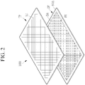
- FIG. 2 illustrates an exploded perspective view of a light emitting display device according to an exemplary embodiment of the present inventive concepts
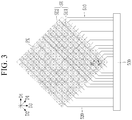
- FIG. 3 illustrates an enlarged top plan view of a partial region of FIG. 2 according to an exemplary embodiment of the present inventive concepts.
- the light emitting display device 1000 includes a display portion DP and a touch portion TP.
- the display portion DP and the touch portion TP are shown in a form such that they are separated from each other for convenience of description, the display portion DP and the touch portion TP according to the exemplary embodiment of the present inventive concepts are integrally formed.
- the light emitting display device 1000 according to an exemplary embodiment of the present inventive concepts will be described as having an on-cell structure in which the touch portion TP is directly disposed on the display portion DP without a separate substrate.
- exemplary embodiments of the present inventive concepts are not limited thereto, and an in-cell structure in which the touch portion TP is formed in the display portion DP may be provided.
- the display portion DP may be divided into a display area DA and a non-display area NDA.
- the display portion DP includes a plurality of pixels PX arranged in a matrix form in the display area DA.
- the plurality of pixels PX according to an exemplary embodiment of the present inventive concepts are illustrated as having a rhombus shape. However, exemplary embodiments of the present inventive concepts are not limited thereto.
- the plurality of pixels PX may have various shapes such as circular shapes, polygonal shapes, etc.
- the touch portion TP is disposed on the display portion DP.
- the touch portion TP includes one or more sensing electrodes SE for detecting presence or absence of touch and touch coordinates.
- the sensing electrode SE may include a first sensing electrode SE1 extending in a first direction D1, and a second sensing electrode SE2 extending in a second direction D2 crossing the first direction D1.
- the first sensing electrode SE1 and the second sensing electrode SE2 may be disposed to surround the pixel PX in a plan view.
- one pixel PX may be surrounded by the first sensing electrode SE1 and the second sensing electrode SE2.
- two first sensing electrodes SE1 and two second sensing electrodes SE2 may surround a pixel PX to fully surround the pixel.
- exemplary embodiments of the present inventive concepts are not limited thereto and the configuration of the first sensing electrode SE1 and the second sensing electrode SE2 surrounding pixels may vary.
- a pair of adjacent first sensing electrode SE1 and a pair of adjacent second sensing electrode SE2 may be disposed to surround four pixels PX forming one pixel group in a plan view.
- the accuracy of touch sensing may vary depending on a degree of density of the first sensing electrode SE1 and the second sensing electrode SE2.
- first sensing electrode SE1 and the second sensing electrode SE2 are illustrated as having a mesh electrode shape in a plan view, exemplary embodiments of the present inventive concepts are not limited thereto.
- first sensing electrode SE1 and the second sensing electrode SE2 may have a surface electrode shape, respectively.
- the first sensing electrode SE1 and the second sensing electrode SE2 may each include a metal or a transparent conductive oxide (TCO).
- the transparent conductive oxide (TCO) may include at least one material selected from an indium tin oxide (ITO), an indium zinc oxide (IZO), a zinc oxide (ZnO), carbon nanotubes (CNT), and graphene.
- the first sensing electrode SE1 is electrically connected to a first routing wire 510
- the second sensing electrode SE2 is electrically connected to a second routing wire 520.
- the first routing wire 510 and the second routing wire 520 may extend substantially along a third direction D3, respectively.
- exemplary embodiments of the present inventive concepts are not limited thereto.
- the first routing wire 510 and the second routing wire 520 are respectively connected to a touch driver 500.
- the first routing wire 510 and the second routing wire 520 are illustrated as being connected to one touch driver 500, respectively, exemplary embodiments of the present inventive concepts are not limited thereto.
- the first routing wire 510 and the second routing wire 520 may be respectively connected to separate touch drivers 500.
- the touch driver 500 may input a driving signal to the first sensing electrode SE1, and determine the presence or absence of the touch and the touch coordinate by using a capacitance change amount or a voltage change amount measured at the second sensing electrode SE2.
- the touch driver 500 may be directly disposed on a substrate as an integrated circuit (IC), or may be formed to have a separate configuration.
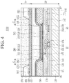
- FIG. 4 illustrates a cross-sectional view of a light emitting display device taken along line IV-IV' of FIG. 3
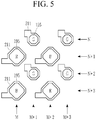
- FIG. 5 illustrates a schematic top plan view of a plurality of first electrodes and a plurality of first openings according to an exemplary embodiment of the present inventive concepts.
- the light emitting display device 1000 includes the display portion DP and the touch portion TP disposed on the display portion DP.
- the display portion DP includes a substrate 110, a driving circuit portion 130, a partition wall 190, a light emitting diode 210, and a thin film encapsulation layer 301.
- the substrate 110 may be made of an insulating material such as glass, quartz, ceramic, and plastic. However, exemplary embodiments of the present inventive concepts are not limited thereto.
- the substrate 110 may be flexible.
- a buffer layer 120 is disposed on the substrate 110.
- a bottom surface of the buffer layer 120 may directly contact a top surface of the substrate 110.
- the buffer layer 120 may include an inorganic film or an organic film, and may have a multi-layered structure.
- the buffer layer 120 prevents impurities, moisture, and the like from penetrating into the driving circuit portion 130 and the light emitting diode 210, and simultaneously flattens the surface.
- the buffer layer 120 may be omitted.
- the driving circuit portion 130 is positioned on the buffer layer 120.
- a bottom surface of the driving circuit portion 130 may be disposed directly on an upper surface of the buffer layer 120.
- the driving circuit portion 130 includes a plurality of thin film transistors 20 and capacitors 80 to drive the light emitting diode 210.
- the driving circuit portion 130 may include a gate line positioned along one direction, and a data line 171 and a common power line 172 that are insulated from and cross the gate line.
- the light emitting diode 210 emits light according to a driving signal received from the driving circuit portion 130 to display an image.
- the light emitting display device 1000 may have a 2Tr-1Cap structure in which two thin film transistors 20 and one capacitor 80 are provided in one pixel PX, or may have various structures in which three or more thin film transistors 20 and two or more capacitors 80 are provided in one pixel PX.
- exemplary embodiments of the present inventive concepts are not limited thereto.
- the capacitor 80 includes a pair of capacitor plates 158 and 178 disposed with an interlayer insulating film 145 therebetween.
- the interlayer insulating film 145 becomes a dielectric.
- the capacity of the capacitor is determined by an electric charge stored in the capacitor 80 and a voltage between the two capacitor plates 158 and 178.
- the thin film transistor 20 includes a semiconductor layer 132, a gate electrode 155, a source electrode 176, and a drain electrode 177.
- the semiconductor layer 132 and the gate electrode 155 are insulated by a gate insulating film 140 that is disposed therebetween.
- a lower surface of the gate insulating film 140 directly contacts an upper surface of the semiconductor layer 132 and an upper surface of the gate insulating film 140 directly contacts a lower surface of the gate electrode 155.
- the light emitting diode 210 may include a first electrode 211, a light emitting layer 212 and a second electrode 213. As shown in the exemplary embodiment of FIG.
- an upper surface of the light emitting layer 212 may directly contact a lower surface of the second electrode 213 and a lower surface of the light emitting layer 212 may directly contact an upper surface of the first electrode 211.
- the thin film transistor 20 applies driving power to the first electrode 211 for emitting light from the light emitting layer 212 of the light emitting diode 210 in a selected pixel PX.
- the gate electrode 155 is connected to the capacitor plate 158
- the source electrode 176 and the other capacitor plate 178 are respectively connected to the common power line 172
- the drain electrode 177 is connected to the first electrode 211 of the light emitting diode 210 through an opening located in a planarization film 146.
- the planarization film 146 is positioned on the interlayer insulating film 145. For example, as shown in the exemplary embodiment of FIG. 4 , a lower surface of the planarization film 146 may directly contact an upper surface of the interlayer insulating film 145.
- the planarization film 146 is made of an insulating material and protects the driving circuit portion 130.
- the planarization film 146 and the interlayer insulating film 145 may include the same material.
- exemplary embodiments of the present inventive concepts are not limited thereto.
- the first electrode 211 is positioned on the planarization film 146.
- the first electrode 211 may be a pixel electrode and may be an anode.
- the first electrode 211 is conductive, and may be a transmissive electrode, a transflective electrode, or a reflective electrode.
- the partition wall 190 is formed on the planarization film 146 to partition a light emitting region.
- a lower surface of the partition wall 190 may directly contact an upper surface of the planarization film 146.
- the light emitting region is also referred to as a pixel region.
- the partition wall 190 may include a polymer organic material.
- the partition wall 190 may include at least one material selected from a polyimide (PI)-based resin, a polyacrylic-based resin, a PET resin, and a PEN resin.
- PI polyimide
- PI polyacrylic-based resin
- PET resin PET resin
- PEN resin a PEN resin
- the partition wall 190 may include a first opening 195, and the first opening 195 may overlap the first electrode 211 (e.g., in a direction of the thickness of the substrate 110).
- the first electrode 211 partially overlaps the partition wall 190, and does not overlap the partition wall 190 in the first opening 195.
- the first opening 195 may be defined as a region of an upper portion of the first electrode 211 that does not overlap the partition wall 190.
- a portion where the partition wall 190 and the first electrode 211 contact each other in the first opening 195 is defined as an edge of the first opening 195.
- the partition wall 190 includes a plurality of first openings 195 respectively corresponding to the plurality of pixels PX.
- the plurality of pixels PX includes a red pixel R emitting red light, a green pixel G emitting green light, and a blue pixel B emitting blue light.
- the organic light emitting diode 210 of the red pixel R includes a red light emitting layer
- the green light emitting diode 210 of the green pixel G includes a green light emitting layer
- the blue light emitting diode 210 of the blue pixel B includes a blue light emitting layer.
- the plurality of pixels PX may include pixels emitting cyan, magenta, and yellow.
- each of the plurality of first openings 195 may have a shape that is similar to the shape of the first electrode 211 in a plan view.
- the edge of the first opening 195 and the first electrode 211 may each have an octagonal shape similar to a rhombus in a plan view (e.g., in a plane parallel to the upper surface of the substrate 110).
- the plurality of first electrodes 211 corresponding to each of the red pixel R, the green pixel G, and the blue pixel B may have different sizes in a plan view (e.g., length in a direction parallel to the upper surface of the substrate 110).
- the plurality of first openings 195 corresponding to each of the red pixel R, the green pixel G, and the blue pixel B may have different sizes in a plan view (e.g., length in a direction parallel to the upper surface of the substrate 110). For example, as shown in FIG.
- the first opening 195 and the first electrodes 211 corresponding to the red pixels R may be respectively formed to have a larger size than the size of the first opening 195 and the first electrodes 211 corresponding to the green pixels G in a plan view.
- the first opening 195 and the first electrodes 211 corresponding to the red pixels R may be respectively formed to have a size that is smaller than or equal to the size of the first opening 195 and the first electrode 211 corresponding to the blue pixel B.
- exemplary embodiments of the present inventive concepts are not limited thereto, and each of the first opening 195 and the first electrodes 211 may be formed to have various sizes.
- the light emitting display device 1000 may have a pentile structure.
- exemplary embodiments of the present inventive concepts are not limited thereto.
- a plurality of first electrodes 211 corresponding to the green light emitting layer are disposed to be spaced apart by a predetermined gap
- the first electrode 211 corresponding to the red light emitting layer and the first electrode 211 corresponding to the blue light emitting layer may be alternately disposed.
- a plurality of first electrodes 211 corresponding to the green light emitting layer are disposed to be spaced apart by a predetermined gap, and in an adjacent (N+3)-th row, the first electrode 211 corresponding to the blue light emitting layer and the first electrode 211 corresponding to the red light emitting layer may be alternately disposed.
- the first electrode 211 corresponding to the plurality of green light emitting layers disposed in the N-th row may be alternately disposed with the first electrode 211 corresponding to the plurality of red and blue light emitting layers disposed in the (N+1)-th row.
- the first electrodes 211 corresponding to the red and blue light emitting layers may be alternately disposed in an M-th column, and the first electrodes 211 corresponding to the plurality of green light emitting layers may be disposed to be spaced apart by a predetermined gap in an adjacent (M+1)-th column.
- the first electrodes 211 corresponding to the blue and red light emitting layers may be alternately disposed in an adjacent (M+2)-th column, and the first electrodes 211 corresponding to the plurality of green light emitting layers may be disposed to be spaced apart by a predetermined gap in an adjacent (M+3)-th column.
- the plurality of first electrodes 211 may be repeatedly disposed on the substrate 110 to have the above-described structure.
- exemplary embodiments of the present inventive concepts are not limited thereto.
- the light emitting layer 212 is positioned on the first electrode 211.
- the light emitting layer 212 may be positioned in the first opening 195 of the partition wall 190 and overlap the first electrode 211 (e.g., in a direction of the thickness of the substrate 110).
- the light emitting layer 212 includes a light emitting material.
- the light emitting material may be an organic material or an inorganic material such as a quantum dot.
- the light emitting layer 212 may include a host and a light emitting dopant.
- exemplary embodiments of the present inventive concepts are not limited thereto.
- a second electrode 213 is positioned on the light emitting layer 212.
- the second electrode 213 may be a common electrode and may be a cathode.
- the second electrode 213 may be a transmissive electrode, a transflective electrode, or a reflective electrode.
- At least one of a hole injection layer HIL and a hole transport layer HTL may be further disposed between the first electrode 211 and the light emitting layer 212, and at least one of an electron transport layer ETL and an electron injection layer EIL may be further disposed between the light emitting layer 212 and the second electrode 213.
- the thin film encapsulation layer 301 is disposed on the second electrode 213 to protect the light emitting diode 210.
- the thin film encapsulation layer 301 prevents external contaminants such as moisture or oxygen from penetrating into the organic light emitting diode 210.
- the thin film encapsulation layer 301 may include at least one inorganic film and at least one organic film 320.
- the thin film encapsulation layer 301 may include a first inorganic film 310 and a second inorganic film 330 and one organic film 320.
- an upper surface of the organic film 320 may directly contact a lower surface of the second inorganic film 330 and a lower surface of the organic film 320 may directly contact an upper surface of the first inorganic film 310.
- exemplary embodiments of the present inventive concepts are not limited thereto.
- the first and second inorganic films 310 and 330 include one or more inorganic materials selected from Al 2 O 3 , TiO 2 , ZrO, SiO 2 , AlON, AlN, SiON, Si 3 N 4 , ZnO, and Ta 2 O 5 .
- the organic film 320 may include a polymer-based material.
- Polymer-based materials include an acrylic resin, an epoxy resin, polyimide, and polyethylene.
- exemplary embodiments of the present inventive concepts are not limited thereto.
- the dense first and second inorganic films 310 and 330 mainly suppress penetration of moisture or oxygen. Any moisture and oxygen that passes through the first and second inorganic films 310 and 330 are again blocked by the organic film 320.
- the organic film 320 also serves as a buffer layer to reduce stress between respective films between the first and second inorganic films 310 and 330 in addition to suppressing moisture penetration.
- a top surface of the thin film encapsulation layer 301 may be planarized by the organic film 320.
- the thin film encapsulation layer 301 may have a thickness of about 5 ⁇ m to about 50 ⁇ m. In embodiments in which the thickness of the thin film encapsulation layer 301 is less than 5 ⁇ m or exceeds 50 ⁇ m, light emitting efficiency of the light emitting display device 1000 may decrease.
- the touch portion TP is disposed on the display portion DP including the substrate 110, the driving circuit portion 130, the partition wall 190, the light emitting diode 210, and the thin film encapsulation layer 301.
- a bottom surface of the touch portion TP may be disposed directly on an upper surface of the second inorganic film 330 of the thin film encapsulation layer 301.
- the first sensing electrode SE1 is positioned on the thin film encapsulation layer 301.
- the first sensing electrode SE1 may include a metal or a transparent conductive oxide (TCO).
- the transparent conductive oxide (TCO) may include at least one compound selected from an indium tin oxide (ITO), an indium zinc oxide (IZO), a zinc oxide (ZnO), carbon nanotubes (CNT), and graphene.
- a first insulating layer 410 is positioned on the thin film encapsulation layer 301 in which the first sensing electrode SE1 is located.
- a lower surface of the first insulating layer 410 may directly contact an upper surface of the second inorganic film 330 of the thin film encapsulation layer 301 and side and upper surfaces of the first sensing electrode SE1.
- the first insulating layer 410 may include at least one of an inorganic film and an organic film.
- the inorganic film may include at least one of a metal oxide, a metal oxynitride, a silicon oxide, a silicon nitride, and a silicon oxynitride.
- the organic film may include a polymer-based material.
- the second sensing electrode SE2 is positioned on the first insulating layer 410.
- the second sensing electrode SE2 may include a metal or a transparent conductive oxide (TCO).
- the transparent conductive oxide (TCO) may include at least one of an indium tin oxide (ITO), an indium zinc oxide (IZO), a zinc oxide (ZnO), carbon nanotubes (CNT), and graphene.
- ITO indium tin oxide
- IZO indium zinc oxide
- ZnO zinc oxide
- CNT carbon nanotubes
- graphene graphene
- the touch portion TP has been described as including the first sensing electrode SE1 and the second sensing electrode SE2 that are disposed on different layers, exemplary embodiments of the touch portion TP are not limited thereto.
- the touch portion TP may include the first sensing electrode SE1 and the second sensing electrode SE2 disposed on the same layer and connected to each other by using a bridge electrode.
- a second insulating layer 420 is positioned on the first insulating layer 410 in which the second sensing electrode SE2 is disposed.
- a lower surface of the second insulating layer 420 may directly contact an upper surface of the first insulating layer and side and upper surfaces of the second sensing electrode SE2.
- the second insulating layer 420 may include at least one of an organic film and an inorganic film.
- a low refractive layer 450 is positioned on the second insulating layer 420.
- a lower surface of the low refractive layer 450 may directly contact an upper surface of the second insulating layer 420.
- the low refractive layer 450 may include a light transmissive organic material having a low refractive index.
- the low refractive layer 450 may include at least one material selected from an acrylic resin, a polyimide resin, a polyamide resin, and Alq3 [tris(8-hydroxyquinolinato)aluminum].
- exemplary embodiments of the present inventive concepts are not limited thereto.
- the low refractive layer 450 has a relatively smaller refractive index than a high refractive layer 470 to be described later.
- the low refractive layer 450 may have a refractive index of about 1.40 to about 1.59.
- the low refractive layer 450 includes a second opening 455.
- the second opening 455 overlaps the first opening 195 (e.g., in a direction of the thickness of the substrate 110).
- An edge of the second opening 455 has a shape similar to the shape of an edge of the first opening 195 in a plan view (e.g., in a direction parallel to the upper surface of the substrate 110).
- the edge of the second opening 455 is defined as a boundary at which the low refractive layer 450 contacts the second insulating layer 420.
- a size (e.g., length in a direction parallel to an upper surface of the substrate 110) of the second opening 455 is larger than the size of the first opening 195 in a plan view. This will be described in further detail later.
- a gap G between the second opening 455 and the first opening 195 is measured based on their edges. For example, as shown in the exemplary embodiment of FIG. 4 , a distance (e.g., in a direction parallel to an upper surface of the substrate 110) between the edge of the first opening 195 and the edge of the second opening 255 is the gap G.
- the gap G between the second opening 455 and the first opening 195 may be the shortest distance in a direction parallel to an upper surface of the substrate at the edges of the two openings.
- the high refractive layer 470 is positioned on the second insulating layer 420 and the low refractive layer 450. For example, as shown in the exemplary embodiment of FIG. 4 , a lower surface of the high refractive layer 470 may directly contact upper surfaces of the second insulating layer 420 and the low refractive layer 450.
- the high refractive layer 470 may include a light transmissive organic material having a high refractive index.
- the high refractive layer 470 has a relatively larger refractive index than the low refractive layer 450.
- the high refractive layer 470 may have a refractive index of about 1.60 to about 1.80.
- the high refractive layer 470 may be located in the second opening 455 of the low refractive layer 450. Further, the high refractive layer 470 may be positioned to overlap the second opening 455 of the low refractive layer 450 and an upper portion of the low refractive layer 450 (e.g., in a direction of the thickness of the substrate 110).
- the light emitting display device 1000 may further include a polarizer, an adhesive layer, and a window disposed on the touch portion TP.
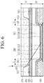
- the touch portion TP includes the low refractive layer 450 including the second opening 455 and the high refractive layer 470 positioned in the second opening 455 of the low refractive layer 450. Therefore, it is possible to improve front visibility and light output efficiency of the light emitting display device 1000. For example, at least some of the light generated by the light emitting diode 210 is reflected at an interface between the low refractive layer 450 and the high refractive layer 470 according to a difference of their refractive indexes. Therefore, the light may be focused in front as will be described in detail with reference to FIG. 6 .
- FIG. 6 illustrates a cross-sectional view of a light emitting display device for explaining reflection of light at an interface between a low refractive layer and a high refractive layer according to an exemplary embodiment of the present inventive concepts.
- light L generated by the light emitting layer 212 may be obliquely incident on the touch portion TP.
- at least some of the light L incident on the high refractive layer 470 of the touch portion TP is reflected at the interface between the low refractive layer 450 and the high refractive layer 470. Particularly, as shown in FIG.
- the incident light L may be totally reflected at the interface between the low refractive layer 450 and the high refractive layer 470.
- the total reflection of light L may occur at the interface between the low refractive layer 450 and the high refractive layer 470.
- the interface between the low refractive layer 450 and the high refractive layer 470 forms an angle of about 40° to about 70° with a line that is parallel to an upper surface of the substrate 110.
- the interface between the low refractive layer 450 and the high refractive layer 470 may be a lateral side surface of the low refractive layer 450 including the second opening 455 (e.g. the lateral side surface of the low refractive layer 450 extending from the edge of the second opening 455 to an uppermost surface of the low refractive layer 450).
- the lateral side surface of the low refractive layer 450 may form an angle of about 40° to about 70° in a cross-sectional view with the second insulating layer 420 on which the low refractive layer 450 is located.
- the angle between the lateral side surface of the low refractive layer 450 and a line that is parallel to an upper surface of the substrate 110 is smaller than 40°, the light L may not be incident on the interface between the low refractive layer 450 and the high refractive layer 470, and thus total reflection may not occur.
- the angle between the lateral side surface of the low refractive layer 450 and the line that is parallel to an upper surface of the substrate 110 is greater than 70°, the light L totally reflected at the interface between the low refractive layer 450 and the high refractive layer 470 may not be emitted to the front of the light emitting display device 1000.
- substantially entire lateral side surface of the low refractive layer 450 is shown as forming an angle of about 40° to about 70° with the second insulating layer 420 in the exemplary embodiment of FIG. 6 , in other exemplary embodiments, a partial portion of the lateral side surface of the low refractive layer 450 may have this angle.
- the interface between the low refractive layer 450 and the high refractive layer 470 forms the angle of about 40° to about 70° with the line parallel to an upper surface of the substrate 110. Therefore, the light L incident on the interface between the low refractive layer 450 and the high refractive layer 470 may be totally reflected. Accordingly, the light L may be focused on the front surface of the light emitting display device 1000, and thus, front visibility and light emitting efficiency thereof may be improved.
- the first opening 195 has a smaller size than the second opening 455 in a plan view (e.g., length in a direction parallel to an upper surface of the substrate 110).
- the gap G between the first opening 195 and the second opening 455 may be about 0.1 ⁇ m to about 2.0 ⁇ m in a plan view (e.g., in a direction parallel to an upper surface of the substrate 110).
- the gap G between the edge of the first opening 195 and the edge of the second opening may always be constant regardless of a direction thereof.
- the display device may include a pixel having a different gap G between the first opening 195 and the second opening 455.
- a first plurality of pixels may have the first gap G1
- a second plurality of pixels may have the second gap.
- a number of the first plurality of pixels having the first gap G1 and a number of the second plurality of pixels having the second gap G2 may be the same and may comprise all of the pixels in the display device.
- the difference between the first gap G1 and the second gap G2 may be in a range of about 0.2 ⁇ m to about 4 ⁇ m.
- the efficiency dispersion of the display device may be reduced by setting two gaps of the respective pixels of the display device.
- FIG. 7 illustrates a pixel having a first gap G1 and a pixel having a second gap G2 according to an embodiment of the present invention.
- the adjacent pixels have a first gap G1 and a second gap G2, respectively, which are different from each other.
- the gaps between the first opening 195 and the second opening 455 in one pixel are always constant regardless of the direction.
- the gap G1 is substantially the same in between the first opening 195 and the second opening 455 in the portions of the gap extending in the first direction D1, second direction D2, third direction D3, and fourth direction D4, respectively.
- some of the plurality of pixels may have the first gap G1 for the length of the gap between the first opening 195 and the second opening 455, and others of the plurality of pixels may have the second gap G2 for the length of the gap between the first opening 195 and the second opening 455.
- the gap G1 is smaller than the gap G2.
- the pixels having the first gap G1 and the second gap G2 may emit light of the same color.
- some thereof may have the first gap G1 and others thereof may have the second gap G2.
- some of the red pixels may have the first gap G1 and others thereof may have the second gap G2.
- some of the green pixels may have the first gap G1 and others thereof may have the second gap G2, and some of the blue pixels may have the first gap G1 and others thereof may have the second gap G2.
- FIG. 8 illustrates a graph showing efficiency dispersion of display devices according to first and second comparative embodiments.
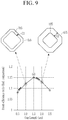
- FIG. 9 illustrates a plan view of a pixel having a first gap and a pixel having a second gap and a graph showing the front efficiency ratio according to the gap size between a second opening of a low refractive layer and a first opening of a partition wall.
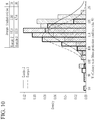
- FIG. 10 illustrates a graph showing efficiency dispersion of display devices according to a second comparative embodiment and a third embodiment in accordance with an exemplary embodiment of the present inventive concepts.
- Example 1 is a comparative embodiment of a display device in which the low refractive layer does not include the second opening and does not include the high refractive layer
- Example 2 is a comparative embodiment of a display device in which the low refractive layer includes the second opening and the gaps are the same in all the pixels.
- Example 3, which is a display device according to the exemplary embodiment of FIG. 1 is a display device in which the low refractive layer includes the second opening and both the pixel having the first gap and the pixel having the second gap exist.
- Example 1 of FIG. 8 is a comparative example of a display device that does not include a total reflection structure at the interface of the low refractive layer 450 and the high refractive layer 470. For example, there is no total reflection at the interface of a low refractive layer and a high refractive layer in the comparative example of Example 1.
- Example 2 is a comparative example of a display device that includes a total reflection structure at the interface of the low refractive layer 450 and the high refractive layer 470 and has gaps having the same size (e.g., length in a direction parallel to an upper surface of the substrate).
- Example 3 is a display device according to an exemplary embodiment of the present inventive concepts that includes a total reflection structure at the interface of the low refractive layer 450 and the high refractive layer 470 and has two different gaps (total reflection, multiple gaps).
- Example 2 having the total reflection structure has improved efficiency as compared to Example 1 having no total reflection structure.
- the efficiency is increased but each efficiency dispersion is widened.
- a standard deviation of Example 1 is about 0.85, but a standard deviation of Example 2 is increased to about 1.8.
- the gaps between the second opening 455 of the low refractive layer 450 and the first opening 195 of the partition wall 190 may vary, such as due to an alignment error of a mask in the manufacturing process.
- the gaps are varied by deviations in the manufacturing process, and such a process deviation results in, as shown in FIG. 8 , an increase in the efficiency dispersion.
- the gaps of respective pixels are specifically designed in the manufacturing process to have different values, that is, to include the first gap G1 and the second gap G2. This may reduce the efficiency dispersion.
- FIG. 9 illustrates a principle in which the efficiency dispersion decreases when the gap is designed with different sizes, such as to include the first gap G1 and the second gap G2, and illustrates the front efficiency ratio according to the gap.
- the graph indicates that the gap between the second opening 455 of the low refractive layer 450 and the first opening 195 of the partition wall 190 is 1.5 ⁇ m, the efficiency is maximal.
- the front efficiency ratio to a reference comparison is equal to about 1.15.
- the gap at which the efficiency becomes the maximum value is defined as a center gap G0.
- the efficiency dispersion may be widened due to the process error.
- the gap between the second opening 455 and the first opening 195 may be formed to be narrower than a design value as a whole.
- the front light emission efficiency moves downward as shown by an arrow in FIG. 9 . That is, when the gap is narrowed due to the process error, the efficiency of the pixel designed at the first gap (1.0 ⁇ m) is reduced.
- FIG. 9 illustrates the case in which the gap is formed to be narrow due to a process error.
- the efficiency may be compensated in the same manner as in FIG. 9 .
- the second gap is formed to be wider than the design value such that the efficiency is correspondingly decreased. Therefore, the decreased efficiency compensates for the increased efficiency.
- the arrows move in a direction opposite to the arrows shown in FIG. 9 .
- FIG. 10 illustrates efficiency dispersion of display devices according to second and third embodiments.
- Example 2 is a display device in which all the gaps have the same design value of 1.3 ⁇ m in all the pixels
- Example 3 which is the display device according to the exemplary embodiment of FIG. 1 , includes a pixel having the first gap (0.8 ⁇ m) and a pixel having the second gap (1.8 ⁇ m).
- the graph indicates that a standard deviation of Example 3 is reduced as compared to the standard deviation of Example 2.
- the standard deviation of Example 2 is illustrated to be 5.389, but it can be confirmed that the standard deviation of Example 3 is reduced to 4.744.
- Example 3 has an efficiency that is slightly reduced as compared to Example 3 (115.9 as compared to 113.6), but this decrease in efficiency is slight and insignificant.
- FIG. 11 illustrates a plan view of the same region as in FIG. 1 for a display device according to another exemplary embodiment.
- the difference between the first gap G1 and the second gap G2 is 1.0 ⁇ m.
- a difference between the first gap G1 and the second gap G2 may be 0.2 ⁇ m.
- the first gap G1 may have a value of (G0 - 0.1) ⁇ m
- the second gap G2 may have a value of (G0 + 0.1) ⁇ m.
- the efficiency dispersion may be reduced by the same principle as in the exemplary embodiments of FIGS. 1 and 9 .
- FIG. 12 illustrates a plan view of the same region as in FIG. 1 for a display device according to another exemplary embodiment.
- the difference between the first and second gaps is 1.0 ⁇ m.
- a difference between the first and second gaps G1, G2 may be 2.0 ⁇ m.
- the first gap G1 may have a value of (G0 - 1.0) ⁇ m
- the second gap G2 may have a value of (G0 + 1.0) ⁇ m.
- the efficiency dispersion may be reduced by the same principle as in the exemplary embodiments of FIG. 1 and 9 .
- FIG. 13 illustrates a plan view of the same region as in FIG. 1 for a display device according to another exemplary embodiment.
- the display device is the same as the exemplary embodiment of FIG. 1 , except that four gaps are provided instead of two gaps.
- a pixel having a difference of 1.0 ⁇ m between the first gap G1 and the second gap G2 and a pixel having a difference of 0.2 ⁇ m between the third gap G3 and the fourth gap G4 may be mixed.
- exemplary embodiments of the present inventive concepts are not limited thereto.
- the difference between the first gap G1 and the second gap G2 and the difference between the third gap G3 and the fourth gap G4 may be variously selected.
- a number of the first plurality of pixels having the first gap G1 and the number of the second plurality of pixels having the second gap G2 are the same, and a number of the third plurality of pixels having the third gap G3 and a number of the fourth plurality of pixels having the fourth gap G4 are the same.
- the pixel having the second gap G2 compensates for the efficiency deviation due to the alignment error of the pixel having the first gap G1
- the pixel having the fourth gap G4 compensates for the efficiency deviation due to the alignment error of the pixel having the third gap G3. Therefore, the efficiency deviation may be reduced.
- an average value of the first gap G1, the second gap G2, the third gap G3, and the fourth gap G4 may be the same.
- the first gap G1 may be (C - 0.5) ⁇ m
- the second gap G2 may be (C + 0.5) ⁇ m
- the third gap G3 may be (C - 0.1) ⁇ m
- the fourth gap G4 may be (C + 0.1) ⁇ m.
- FIG. 13 illustrates a configuration in which the number of gaps is 4, the number of gaps may be greater than 4.
- FIG. 14 illustrates the same region as in FIG. 1 with respect to a display device according to another exemplary embodiment. Referring to the exemplary embodiment shown in FIG. 14 , the display device is the same as the exemplary embodiment of FIG. 13 , except that six gaps are provided instead of four gaps.
- a pixel in which a difference between the first gap G1 and the second gap G2 is 1.0 ⁇ m, a pixel in which a difference between the third gap G3 and the fourth gap G4 is 2.0 ⁇ m, and a pixel in which a difference between a fifth gap G5 and a sixth gap G6 is 0.2 ⁇ m may be mixed.
- exemplary embodiments of the present inventive concepts are not limited thereto.
- the difference between the first gap G1 and the second gap G2, the difference between the third gap G3 and the fourth gap G4, and the difference between the fifth gap G5 and the sixth gap G6 may be variously selected.
- the number of the first plurality of pixels having the first gap G1 and the number of the second plurality of pixels having the second gap G2 are the same
- the number of the third plurality of pixels having the third gap G3 and the number of the fourth plurality of pixels having the fourth gap G4 are the same
- the number of the fifth plurality of pixels having the fifth gap G5 and the number of the sixth plurality of pixels having the sixth gap G6 are the same.
- the pixel having the second gap G2 compensates for the efficiency deviation due to the alignment error of the pixel having the first gap G1
- the pixel having the fourth gap G4 compensates for the efficiency deviation due to the alignment error of the pixel having the third gap G3
- the pixel having the sixth gap G6 compensates for the efficiency deviation due to the alignment error of the pixel having the fifth gap G5. Therefore, the efficiency deviation may be reduced.
- an average value of the first gap G1 and the second gap G2, an average value of the third gap G3 and the fourth gap G4, and an average value of the fifth gap G5 and the sixth gap G6 may be the same.
- the first gap G1 may be (C - 0.5) ⁇ m
- the second gap G2 may be (C + 0.5) ⁇ m
- the third gap G3 may be (C -0.1) ⁇ m
- the fourth gap G4 may be (C + 0.1) ⁇ m
- the fifth gap G5 may be (C - 1.0) ⁇ m
- the sixth gap G6 may be (C + 1.0) ⁇ m.
- FIG. 15 illustrates a plan view of the same region as in FIG. 1 for a display device according to another exemplary embodiment.
- the display device according to the exemplary embodiment of FIG. 15 is the same as the exemplary embodiment of FIG. 13 , except that three gaps of the first gap G1, the second gap G2, and the center gap G0 are included therein. A detailed description of the same components will be omitted.
- the center gap G0 is an average value of the first gap G1 and the second gap G2.
- a pixel having the first gap G1 (X - a) decreased by (a) based on the center gap G0 (X) and a pixel having the second gap G2 (X + a) increased by (a) based on the center gap G0 (X) may be included.
- the number of pixels having the first gap G1 and the number of pixels having the second gap G2 are the same.
- a range of the center gap G0 may be about 0.5 ⁇ m to about 5.0 ⁇ m, and a value of (a) may be about 0.1 ⁇ m to 1.0 ⁇ m.
- the efficiency dispersion may be reduced without greatly reducing the front emission efficiency.
- a pixel having the gap of 1.5 ⁇ m, a pixel having the gap of 0.5 ⁇ m, and a pixel having the gap of 2.0 ⁇ m may be mixed.
- the average efficiency of the pixels having three gaps is increased, and the efficiency deviation due to the process error is compensated by the pixel having the gap of 0.5 ⁇ m and the pixel having the gap of the 2.0 ⁇ m. Therefore, the efficiency dispersion may be reduced.
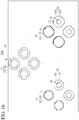
- FIG. 16 illustrates a plan view of the same region as in FIG. 1 for a display device according to another exemplary embodiment of the present inventive concepts.
- the display device according to the exemplary embodiment of FIG. 16 is the same as the exemplary embodiment of FIG. 1 , except that five gaps of the first gap G1, the second gap G2, the third gap G3, the fourth gap G4, and the center gap G0 are included therein.
- the center gap G0 in the exemplary embodiment of FIG. 16 is an average value of the first gap G1 and the second gap G2, and is an average value of the third gap G3 and the fourth gap G4.
- a pixel having the first gap G1 (X- a) decreased by (a) based on the center gap G0 (X) and a pixel having the second gap G2 (X + a) increased by (a) are included, and a pixel having the third gap G3 (X- b) decreased by (b) based on the center gap G0 (X) and a pixel having the fourth gap G4 (X + b) increased by (b) are included.
- a number of the first plurality of pixels having the first gap G1 and a number of the second plurality of pixels having the second gap G2 are the same, and a number of the third plurality of pixels having the third gap G3 and a number of the fourth plurality of pixels having the fourth gap G4 are the same.
- a range of the center gap G0 (X) may be about 0.5 ⁇ m to about 5.0 ⁇ m, and a value of the (a) may be about 0.1 ⁇ m to about 1.0 ⁇ m.
- a range of a value of the (b) may be about 0.1 ⁇ m to about 1.0 ⁇ m.
- the values of the (a) and (b) may not be the same. However, even in the exemplary embodiment of FIG. 16 , the efficiency dispersion may be reduced without greatly reducing the front light emission efficiency through the same principle as in FIG. 15 .
- FIG. 17 illustrates the same region as in FIG. 16 with respect to a display device according to another exemplary embodiment of the present inventive concepts.
- the display device according to the exemplary embodiment of FIG. 17 is the same as the exemplary embodiment of FIG. 1 , except that five gaps of the first gap G1, the second gap G2, the third gap G3, the fourth gap G4, the fifth gap G5, the sixth gap G6, and the center gap G0 are included therein.
- the center gap is an average value of the first gap G1 and the second gap G2, an average value of the third gap G3 and the fourth gap G4, and an average value of the fifth gap G5 and the sixth gap G6.
- the display device includes a pixel having the first gap G1 (X- a) decreased by (a) based on the center gap G0 (X) and a pixel having the second gap G2 (X + a) increased by (a), a pixel having the third gap G3 (X- b) decreased by (b) based on the center gap G0 (X) and a pixel having the fourth gap G4 (X + b) increased by (b), and a pixel having the fifth gap G5 (X- c) decreased by (c) based on the center gap G0 (X) and a pixel having the sixth gap G6 (X + c) increased by (c).
- a number of the first plurality of pixels having the first gap G1 and a number of the second plurality of pixels having the second gap G2 are the same, a number of the third plurality of pixels having the third gap G3 and a number of the fourth plurality of pixels having the fourth gap G4 are the same, and a number of the fifth plurality of pixels having the fifth gap G5 and a number of the sixth plurality of pixels having the sixth gap G6 are the same.
- a range of the median gap G0 (X) may be about 0.5 ⁇ m to about 5.0 ⁇ m
- a range of a value of (a) is about 0.1 ⁇ m to about 1.0 ⁇ m
- a range of a value of (b) may be about 0.1 ⁇ m to about 1.0 ⁇ m
- a range of a value of (c) may be about 0.1 ⁇ m to about 1.0 ⁇ m.
- the values of the (a), (b), and (c) may not be the same. However, even in the exemplary embodiment of FIG. 17 , the efficiency dispersion may be reduced without greatly reducing the front light emission efficiency through the same principle as in the exemplary embodiment of FIG. 15 .
Landscapes
- Engineering & Computer Science (AREA)
- Microelectronics & Electronic Packaging (AREA)
- Physics & Mathematics (AREA)
- Optics & Photonics (AREA)
- Electroluminescent Light Sources (AREA)
Abstract
Description
- The present inventive concepts relate to a display device, and more particularly, to a display device including a touch portion that may improve efficiency dispersion.
- A light emitting display device is a self-luminous display device that displays an image by using a light emitting diode. The light emitting display device provides features including low power consumption, high brightness, and high response speed.
- The display device has a multilayer structure. For example, the display device may have a multilayer structure including a light emitting diode and a touch portion. When light generated by the light emitting diode is emitted to the outside, reflection, total reflection, and the like may occur at an interlayer interface thereof due to the multilayer structure. Some of the light generated by the light emitting diode is dissipated by the reflection, the total reflection, and the like, and thus the light emitting efficiency and display quality of the display device may be degraded.
- In addition, the efficiency dispersion of the display device may vary due to an alignment deviation of respective layers of the multilayer structure.
- The present inventive concepts concern a display device with improved efficiency dispersion.
- An exemplary embodiment of the present inventive concepts provides a display device including a substrate and a plurality of pixels positioned on the substrate. Each pixel includes a first electrode, a partition wall including a first opening overlapping the first electrode, and a low refractive layer including a second opening overlapping the first opening. The plurality of pixels includes a first plurality of pixels having a first gap between an edge of the first opening and an edge of the second opening in a direction parallel to an upper surface of the substrate. The plurality of pixels further includes a second plurality of pixels having a second gap between an edge of the first opening and an edge of the second opening in the direction parallel to the upper surface of the substrate. The first gap and the second gap have different lengths from each other in the direction parallel to the upper surface of the substrate. At least one of the first plurality of pixels and at least one of the second plurality of pixels emit light of the same color as each other.
- A number of pixels having the first gap and a number of pixels having the second gap may be the same.
- Each of the first gap and the second gap may be 0.1 µm to 2 µm.
- In one pixel, distances in a direction parallel to the substrate between the edges of the first opening and the edges of the second opening may be the same in all directions.
- A size of the first opening may be smaller than that of the second opening in a plan view.
- Some of the plurality of pixels may have a third gap between an edge of the first opening and an edge of the second opening in a direction parallel to the substrate, others of the plurality of pixels may have a fourth gap between an edge of the first opening and an edge of the second opening in a direction parallel to the substrate, and the third gap and the fourth gap may have different values.
- An average value of the third gap and the fourth gap and an average value of the first gap and the second gap may be the same.
- Some of the plurality of pixels may have a fifth gap between an edge of the first opening and an edge of the second opening in a direction parallel to the substrate, others of the plurality of pixels may have a sixth gap between an edge of the first opening and an edge of the second opening in a direction parallel to the substrate, and the fifth gap and the sixth gap may have different values.
- An average value of the fifth gap and the sixth gap, an average value of the third gap and the fourth gap, and an average value of the first gap and the second gap may be the same.
- In some of the plurality of pixels, a distance between an edge of the first opening and an edge of the second opening in a direction parallel to the substrate may be an average value of the first gap and the second gap.
- The display device may further include a second electrode overlapping the first electrode, a light emitting layer disposed between the first electrode and the second electrode, a thin film encapsulation layer disposed on the second electrode, and a sensing electrode located on the thin film encapsulation layer, and the low refractive layer may be disposed on the sensing electrode.
- A high refractive layer disposed in the second opening may be further included.
- The low refractive layer may have a refractive index of 1.40 to 1.59, and the high refractive layer may have a refractive index of 1.60 to 1.80.
- Another exemplary embodiment of the present inventive embodiments provides a display device that includes a substrate and a plurality of pixels positioned on the substrate. Each pixel includes a first electrode, a partition wall including a first opening overlapping the first electrode, a low refractive layer including a second opening overlapping the first opening, and a high refractive layer positioned in the second opening. The plurality of pixels includes a first plurality of pixels having a first gap between an edge of the first opening and an edge of the second opening in a direction parallel to an upper surface of the substrate. The plurality of pixels also includes a second plurality of pixels having a second gap between an edge of the first opening and an edge of the second opening in the direction parallel to the upper surface of the substrate. The second gap has a length that is different from a length of the first gap. The plurality of pixels includes a third plurality of pixels having a third gap between an edge of the first opening and an edge of the second opening in the direction parallel to the upper surface of the substrate. The third gap has a length that is equal to an average of the lengths of the first gap and the second gap.
- A pixel having the first gap, a pixel having the second gap, and a pixel having the average gap may emit light of the same color.
- Some of the plurality of pixels may have a third gap between an edge of the first opening and an edge of the second opening in a direction parallel to the substrate, others of the plurality of pixels may have a fourth gap, which is different from the third gap, between an edge of the first opening and an edge of the second opening in a direction parallel to the substrate, and an average value of the third gap and the fourth gap may be the same as that of the first gap and the second gap.
- Some of the plurality of pixels may have a fifth gap between an edge of the first opening and an edge of the second opening in a direction parallel to the substrate, others of the plurality of pixels may have a sixth gap, which is different from the fifth gap, between an edge of the first opening and an edge of the second opening in a direction parallel to the substrate, and an average value of the fifth gap and the sixth gap may be the same as that of the first gap and the second gap.
- Another exemplary embodiment of the present inventive concepts provides a display device that includes a substrate and a plurality of first electrodes positioned on the substrate. A partition wall having a plurality of first openings respectively overlaps the first electrodes. A light emitting layer is positioned in the first openings. A second electrode is disposed on the light emitting layer. A low refractive layer is disposed on the second electrode and includes a second opening overlapping the first opening. A high refractive layer is positioned in the second opening of the low refractive layer. A length of the first opening is smaller than a length of the second opening in a direction parallel to an upper surface of the substrate. The plurality of first electrodes includes a first plurality of first electrodes having a first gap between an edge of the first opening and an edge of the second opening in the direction parallel to the upper surface of the substrate. The plurality of first electrodes also includes a second plurality of first electrodes having a second gap between an edge of the first opening and an edge of the second opening in the direction parallel to the upper surface of the substrate. The second gap has a length that is different from a length of the first gap.
- A color of light emitted from a light emitting layer overlapping the first electrode having the first gap may be the same as that of light emitted from a light emitting layer overlapping the first electrode having the second gap.
- In some of the plurality of first electrodes, a distance between an edge of the first opening and an edge of the second opening in a direction parallel to the substrate may be an average value of the first gap and the second gap.
- According to exemplary embodiments of the present inventive concepts, a display device having improved efficiency dispersion is provided.
-
-
FIG. 1 illustrates a plan view of a display device according to an exemplary embodiment of the present inventive concepts. -
FIG. 2 illustrates an exploded perspective view of a light emitting display device according to an exemplary embodiment of the present inventive concepts. -
FIG. 3 illustrates an enlarged top plan view of a partial region ofFIG. 2 . -
FIG. 4 illustrates a cross-sectional view of a light emitting display device taken along line IV-IV' ofFIG. 3 according to an exemplary embodiment of the present inventive concepts. -
FIG. 5 illustrates a top plan view of a plurality of first electrodes and a plurality of first openings according to an exemplary embodiment of the present inventive concepts. -
FIG. 6 illustrates a cross-sectional view of a light emitting display device according to an exemplary embodiment of the present inventive concepts. -
FIG. 7 illustrates a top plan view of a pixel having a first gap and a pixel having a second gap according to an exemplary embodiment of the present inventive concepts. -
FIG. 8 illustrates a graph showing efficiency dispersion of display devices according to first and second comparative embodiments of the present inventive concepts. -
FIG. 9 illustrates a plan view of a pixel having a first gap and a pixel having a second gap and a graph showing the front efficiency ratio according to the gap size according to an exemplary embodiment of the present inventive concepts. -
FIG. 10 illustrates a graph showing efficiency dispersion of display devices according to a second comparative embodiment and a third exemplary embodiments of the present inventive concepts. -
FIG. 11 illustrates a plan view of a display device according to another exemplary embodiment of the present inventive concepts. -
FIG. 12 illustrates a plan view of a display device according to another exemplary embodiment of the present inventive concepts. -
FIG. 13 illustrates a plan view of a display device according to another exemplary embodiment of the present inventive concepts. -
FIG. 14 illustrates a plan view of a display device according to another exemplary embodiment of the present inventive concepts. -
FIG. 15 illustrates a plan view of a display device according to another exemplary embodiment of the present inventive concepts. -
FIG. 16 illustrates a plan view of a display device according to another exemplary embodiment of the present inventive concepts. -
FIG. 17 illustrates a plan view of a display device according to another exemplary embodiment of the present inventive concepts. - The present invention will be described more fully hereinafter with reference to the accompanying drawings, in which exemplary embodiments of the present inventive concepts are shown. As those skilled in the art would realize, the described exemplary embodiments may be modified in various different ways, all without departing from the spirit or scope of the present inventive concepts.
- Parts that are irrelevant to the description will be omitted to clearly describe the present inventive concepts, and like reference numerals designate like elements throughout the specification.
- Further, in the drawings, the size and thickness of each element are arbitrarily illustrated for ease of description, and the present inventive concepts are not necessarily limited to those illustrated in the drawings. In the drawings, the thicknesses of layers, films, panels, regions, etc., are exaggerated for clarity. In the drawings, for ease of description, the thicknesses of some layers and areas are exaggerated.
- It will be understood that when an element such as a layer, film, region, or substrate is referred to as being "on" another element, it can be directly on the other element or intervening elements may also be present. In contrast, when an element is referred to as being "directly on" another element, there are no intervening elements present. Further, in the specification, the word "on" or "above" means positioned on or below the object portion, and does not necessarily mean positioned on the upper side of the object portion based on a gravitational direction.
- In addition, unless explicitly described to the contrary, the word "comprise" and variations such as "comprises" or "comprising" will be understood to imply the inclusion of stated elements but not the exclusion of any other elements.
- Further, throughout the specification, the phrase "in a plan view" means viewing a target portion from the top, and the phrase "in a cross-section" means viewing a cross-section formed by vertically cutting a target portion from the side.
- Hereinafter, a display device according to an exemplary embodiment of the present inventive concepts will be described in detail with reference to the accompanying drawings.
-
FIG. 1 schematically illustrates adisplay device 1000 according to an exemplary embodiment of the present inventive concepts.FIG. 1 mainly illustrates asecond opening 455 of a lowrefractive layer 450 and afirst opening 195 of apartition wall 190 according to an exemplary embodiment of the present inventive concepts. A detailed configuration of all pixels including the lowrefractive layer 450 and thepartition wall 190 will be described in detail later with reference to other drawings. Referring toFIG. 1 , thefirst opening 195 is a region in which a light emitting diode layer is positioned and light is emitted thereby, and thesecond opening 455 of the lowrefractive layer 450 is a layer that induces total reflection of light emitted from the light emitting diode layer to improve the light emitting efficiency. Thefirst opening 195 and thesecond opening 455 form one pixel PX. - In
FIG. 1 , gaps G1 and G2 between edges of thefirst opening 195 and edges of thesecond opening 455 are different. In the present specification, the gap between an edge of thefirst opening 195 and an adjacent edge of thesecond opening 455 will be referred to as a gap. For example, unless otherwise described, the gap, which is a term used herein, means a distance between the edge of thefirst opening 195 and the edge of thesecond opening 455. The distance may be a shortest distance in a direction parallel to the substrate. - In the display device according to an exemplary embodiment of the present inventive concepts, the gap of a first plurality of the pixels is the first distance G1, and the gap of a second plurality of the pixels is the second distance G2. In an exemplary embodiment, among all the pixels of the display device, the number of the first plurality of pixels having a gap with the first distance G1 and a number of the second plurality of pixels having a gap with the second distance G2 are the same. In an exemplary embodiment, a difference between the first gap G1 and the second gap G2 may be about 1 µm. However, exemplary embodiments of the present inventive concepts are not limited thereto. For example, in other exemplary embodiments, the difference between the first gap G1 and the second gap G2 may be about 0.2 µm to about 4 µm. Efficiency dispersion may be the dispersion of different front light emission efficiency values for a plurality of pixels. The differences in the front light emission efficiency values may be based on differences in the gap sizes of the pixels. The efficiency dispersion of the display device may be reduced by including pixels having gaps with two or more different values (e.g., lengths). The effects of efficiency dispersion of the display device due to the pixels having gaps with two or more different values will be described later.
- Hereinafter, a detailed structure of the display device according to an exemplary embodiment of the present inventive concepts will be described in detail.
-
FIG. 2 illustrates an exploded perspective view of a light emitting display device according to an exemplary embodiment of the present inventive concepts, andFIG. 3 illustrates an enlarged top plan view of a partial region ofFIG. 2 according to an exemplary embodiment of the present inventive concepts. - Referring to
FIG. 2 , the light emittingdisplay device 1000 according to an exemplary embodiment of the present inventive concepts includes a display portion DP and a touch portion TP. In this embodiment, although the display portion DP and the touch portion TP are shown in a form such that they are separated from each other for convenience of description, the display portion DP and the touch portion TP according to the exemplary embodiment of the present inventive concepts are integrally formed. For example, the light emittingdisplay device 1000 according to an exemplary embodiment of the present inventive concepts will be described as having an on-cell structure in which the touch portion TP is directly disposed on the display portion DP without a separate substrate. However, exemplary embodiments of the present inventive concepts are not limited thereto, and an in-cell structure in which the touch portion TP is formed in the display portion DP may be provided. - The display portion DP may be divided into a display area DA and a non-display area NDA. The display portion DP includes a plurality of pixels PX arranged in a matrix form in the display area DA. The plurality of pixels PX according to an exemplary embodiment of the present inventive concepts are illustrated as having a rhombus shape. However, exemplary embodiments of the present inventive concepts are not limited thereto. For example, in other exemplary embodiments, the plurality of pixels PX may have various shapes such as circular shapes, polygonal shapes, etc.
- The touch portion TP is disposed on the display portion DP. The touch portion TP includes one or more sensing electrodes SE for detecting presence or absence of touch and touch coordinates.
- Referring to the exemplary embodiment shown in
FIG. 3 , the sensing electrode SE may include a first sensing electrode SE1 extending in a first direction D1, and a second sensing electrode SE2 extending in a second direction D2 crossing the first direction D1. - In an exemplary embodiment, the first sensing electrode SE1 and the second sensing electrode SE2 may be disposed to surround the pixel PX in a plan view.
- For example, as shown in the exemplary embodiment of
FIG. 3 , one pixel PX may be surrounded by the first sensing electrode SE1 and the second sensing electrode SE2. For example, as shown in the exemplary embodiment ofFIG. 3 , two first sensing electrodes SE1 and two second sensing electrodes SE2 may surround a pixel PX to fully surround the pixel. However, exemplary embodiments of the present inventive concepts are not limited thereto and the configuration of the first sensing electrode SE1 and the second sensing electrode SE2 surrounding pixels may vary. For example, in another exemplary embodiment, a pair of adjacent first sensing electrode SE1 and a pair of adjacent second sensing electrode SE2 may be disposed to surround four pixels PX forming one pixel group in a plan view. The accuracy of touch sensing may vary depending on a degree of density of the first sensing electrode SE1 and the second sensing electrode SE2. - In addition, although the first sensing electrode SE1 and the second sensing electrode SE2 are illustrated as having a mesh electrode shape in a plan view, exemplary embodiments of the present inventive concepts are not limited thereto. For example, in another exemplary embodiment, the first sensing electrode SE1 and the second sensing electrode SE2 may have a surface electrode shape, respectively.
- In an exemplary embodiment, the first sensing electrode SE1 and the second sensing electrode SE2 may each include a metal or a transparent conductive oxide (TCO). For example, the transparent conductive oxide (TCO) may include at least one material selected from an indium tin oxide (ITO), an indium zinc oxide (IZO), a zinc oxide (ZnO), carbon nanotubes (CNT), and graphene.
- The first sensing electrode SE1 is electrically connected to a
first routing wire 510, and the second sensing electrode SE2 is electrically connected to asecond routing wire 520. As shown in the exemplary embodiment ofFIG. 3 , thefirst routing wire 510 and thesecond routing wire 520 may extend substantially along a third direction D3, respectively. However, exemplary embodiments of the present inventive concepts are not limited thereto. - The
first routing wire 510 and thesecond routing wire 520 are respectively connected to atouch driver 500. Although thefirst routing wire 510 and thesecond routing wire 520 are illustrated as being connected to onetouch driver 500, respectively, exemplary embodiments of the present inventive concepts are not limited thereto. For example, in other exemplary embodiments, thefirst routing wire 510 and thesecond routing wire 520 may be respectively connected to separatetouch drivers 500. - The
touch driver 500 may input a driving signal to the first sensing electrode SE1, and determine the presence or absence of the touch and the touch coordinate by using a capacitance change amount or a voltage change amount measured at the second sensing electrode SE2. In an exemplary embodiment, thetouch driver 500 may be directly disposed on a substrate as an integrated circuit (IC), or may be formed to have a separate configuration. -
FIG. 4 illustrates a cross-sectional view of a light emitting display device taken along line IV-IV' ofFIG. 3 , andFIG. 5 illustrates a schematic top plan view of a plurality of first electrodes and a plurality of first openings according to an exemplary embodiment of the present inventive concepts. - Referring to the exemplary embodiment of
FIG. 4 , the light emittingdisplay device 1000 includes the display portion DP and the touch portion TP disposed on the display portion DP. - The display portion DP includes a
substrate 110, a drivingcircuit portion 130, apartition wall 190, alight emitting diode 210, and a thinfilm encapsulation layer 301. - In an exemplary embodiment, the
substrate 110 may be made of an insulating material such as glass, quartz, ceramic, and plastic. However, exemplary embodiments of the present inventive concepts are not limited thereto. Thesubstrate 110 may be flexible. - A
buffer layer 120 is disposed on thesubstrate 110. For example, as shown in the exemplary embodiment ofFIG. 4 , a bottom surface of thebuffer layer 120 may directly contact a top surface of thesubstrate 110. In an exemplary embodiment, thebuffer layer 120 may include an inorganic film or an organic film, and may have a multi-layered structure. Thebuffer layer 120 prevents impurities, moisture, and the like from penetrating into the drivingcircuit portion 130 and thelight emitting diode 210, and simultaneously flattens the surface. However, in another exemplary embodiment of the present inventive concepts, thebuffer layer 120 may be omitted. - The driving
circuit portion 130 is positioned on thebuffer layer 120. For example, as shown in the exemplary embodiment ofFIG. 4 , a bottom surface of the drivingcircuit portion 130 may be disposed directly on an upper surface of thebuffer layer 120. The drivingcircuit portion 130 includes a plurality ofthin film transistors 20 andcapacitors 80 to drive thelight emitting diode 210. In addition, the drivingcircuit portion 130 may include a gate line positioned along one direction, and adata line 171 and acommon power line 172 that are insulated from and cross the gate line. - The
light emitting diode 210 emits light according to a driving signal received from the drivingcircuit portion 130 to display an image. - In an exemplary embodiment of the present inventive concepts, the light emitting
display device 1000 may have a 2Tr-1Cap structure in which twothin film transistors 20 and onecapacitor 80 are provided in one pixel PX, or may have various structures in which three or morethin film transistors 20 and two ormore capacitors 80 are provided in one pixel PX. However, exemplary embodiments of the present inventive concepts are not limited thereto. - The
capacitor 80 includes a pair ofcapacitor plates interlayer insulating film 145 therebetween. In this embodiment, theinterlayer insulating film 145 becomes a dielectric. The capacity of the capacitor is determined by an electric charge stored in thecapacitor 80 and a voltage between the twocapacitor plates - The
thin film transistor 20 includes asemiconductor layer 132, agate electrode 155, asource electrode 176, and adrain electrode 177. Thesemiconductor layer 132 and thegate electrode 155 are insulated by agate insulating film 140 that is disposed therebetween. For example, as shown in the exemplary embodiment ofFIG. 4 , a lower surface of thegate insulating film 140 directly contacts an upper surface of thesemiconductor layer 132 and an upper surface of thegate insulating film 140 directly contacts a lower surface of thegate electrode 155. Thelight emitting diode 210 may include afirst electrode 211, alight emitting layer 212 and asecond electrode 213. As shown in the exemplary embodiment ofFIG. 4 , an upper surface of thelight emitting layer 212 may directly contact a lower surface of thesecond electrode 213 and a lower surface of thelight emitting layer 212 may directly contact an upper surface of thefirst electrode 211. Thethin film transistor 20 applies driving power to thefirst electrode 211 for emitting light from thelight emitting layer 212 of thelight emitting diode 210 in a selected pixel PX. In this embodiment, thegate electrode 155 is connected to thecapacitor plate 158, thesource electrode 176 and theother capacitor plate 178 are respectively connected to thecommon power line 172, and thedrain electrode 177 is connected to thefirst electrode 211 of thelight emitting diode 210 through an opening located in aplanarization film 146. - The
planarization film 146 is positioned on theinterlayer insulating film 145. For example, as shown in the exemplary embodiment ofFIG. 4 , a lower surface of theplanarization film 146 may directly contact an upper surface of theinterlayer insulating film 145. Theplanarization film 146 is made of an insulating material and protects the drivingcircuit portion 130. In an exemplary embodiment, theplanarization film 146 and theinterlayer insulating film 145 may include the same material. However, exemplary embodiments of the present inventive concepts are not limited thereto. - The
first electrode 211 is positioned on theplanarization film 146. Thefirst electrode 211 may be a pixel electrode and may be an anode. Thefirst electrode 211 is conductive, and may be a transmissive electrode, a transflective electrode, or a reflective electrode. - The
partition wall 190 is formed on theplanarization film 146 to partition a light emitting region. For example, as shown in the exemplary embodiment ofFIG. 4 , a lower surface of thepartition wall 190 may directly contact an upper surface of theplanarization film 146. In this embodiment, the light emitting region is also referred to as a pixel region. In an exemplary embodiment, thepartition wall 190 may include a polymer organic material. For example, thepartition wall 190 may include at least one material selected from a polyimide (PI)-based resin, a polyacrylic-based resin, a PET resin, and a PEN resin. However, exemplary embodiments of the present inventive concepts are not limited thereto. - The
partition wall 190 may include afirst opening 195, and thefirst opening 195 may overlap the first electrode 211 (e.g., in a direction of the thickness of the substrate 110). Thefirst electrode 211 partially overlaps thepartition wall 190, and does not overlap thepartition wall 190 in thefirst opening 195. Thefirst opening 195 may be defined as a region of an upper portion of thefirst electrode 211 that does not overlap thepartition wall 190. In addition, a portion where thepartition wall 190 and thefirst electrode 211 contact each other in thefirst opening 195 is defined as an edge of thefirst opening 195. - Referring to
FIG. 5 , thepartition wall 190 includes a plurality offirst openings 195 respectively corresponding to the plurality of pixels PX. In an exemplary embodiment, the plurality of pixels PX includes a red pixel R emitting red light, a green pixel G emitting green light, and a blue pixel B emitting blue light. In this embodiment, the organiclight emitting diode 210 of the red pixel R includes a red light emitting layer, the greenlight emitting diode 210 of the green pixel G includes a green light emitting layer, and the bluelight emitting diode 210 of the blue pixel B includes a blue light emitting layer. However, exemplary embodiments of the present inventive concepts are not limited thereto. For example, in another exemplary embodiment, the plurality of pixels PX may include pixels emitting cyan, magenta, and yellow. - Referring to the exemplary embodiment of
FIG. 5 , each of the plurality offirst openings 195 may have a shape that is similar to the shape of thefirst electrode 211 in a plan view. For example, as shown inFIG. 5 , the edge of thefirst opening 195 and thefirst electrode 211 may each have an octagonal shape similar to a rhombus in a plan view (e.g., in a plane parallel to the upper surface of the substrate 110). - In this embodiment, the plurality of
first electrodes 211 corresponding to each of the red pixel R, the green pixel G, and the blue pixel B may have different sizes in a plan view (e.g., length in a direction parallel to the upper surface of the substrate 110). Similarly, the plurality offirst openings 195 corresponding to each of the red pixel R, the green pixel G, and the blue pixel B may have different sizes in a plan view (e.g., length in a direction parallel to the upper surface of the substrate 110). For example, as shown inFIG. 5 , thefirst opening 195 and thefirst electrodes 211 corresponding to the red pixels R may be respectively formed to have a larger size than the size of thefirst opening 195 and thefirst electrodes 211 corresponding to the green pixels G in a plan view. Thefirst opening 195 and thefirst electrodes 211 corresponding to the red pixels R may be respectively formed to have a size that is smaller than or equal to the size of thefirst opening 195 and thefirst electrode 211 corresponding to the blue pixel B. However, exemplary embodiments of the present inventive concepts are not limited thereto, and each of thefirst opening 195 and thefirst electrodes 211 may be formed to have various sizes. - In addition, the light emitting
display device 1000 according to an exemplary embodiment may have a pentile structure. However, exemplary embodiments of the present inventive concepts are not limited thereto. For example, as shown inFIG. 5 , in an N-th row, a plurality offirst electrodes 211 corresponding to the green light emitting layer are disposed to be spaced apart by a predetermined gap, and in an adjacent (N+1)-th row, thefirst electrode 211 corresponding to the red light emitting layer and thefirst electrode 211 corresponding to the blue light emitting layer may be alternately disposed. In a like manner, in an adjacent (N+2)-th row, a plurality offirst electrodes 211 corresponding to the green light emitting layer are disposed to be spaced apart by a predetermined gap, and in an adjacent (N+3)-th row, thefirst electrode 211 corresponding to the blue light emitting layer and thefirst electrode 211 corresponding to the red light emitting layer may be alternately disposed. - In addition, the
first electrode 211 corresponding to the plurality of green light emitting layers disposed in the N-th row may be alternately disposed with thefirst electrode 211 corresponding to the plurality of red and blue light emitting layers disposed in the (N+1)-th row. For example, thefirst electrodes 211 corresponding to the red and blue light emitting layers may be alternately disposed in an M-th column, and thefirst electrodes 211 corresponding to the plurality of green light emitting layers may be disposed to be spaced apart by a predetermined gap in an adjacent (M+1)-th column. In a like manner, thefirst electrodes 211 corresponding to the blue and red light emitting layers may be alternately disposed in an adjacent (M+2)-th column, and thefirst electrodes 211 corresponding to the plurality of green light emitting layers may be disposed to be spaced apart by a predetermined gap in an adjacent (M+3)-th column. For example, the plurality offirst electrodes 211 may be repeatedly disposed on thesubstrate 110 to have the above-described structure. However, exemplary embodiments of the present inventive concepts are not limited thereto. - Referring to the exemplary embodiment of
FIG. 4 , thelight emitting layer 212 is positioned on thefirst electrode 211. Thelight emitting layer 212 may be positioned in thefirst opening 195 of thepartition wall 190 and overlap the first electrode 211 (e.g., in a direction of the thickness of the substrate 110). - The
light emitting layer 212 includes a light emitting material. In an exemplary embodiment, the light emitting material may be an organic material or an inorganic material such as a quantum dot. In addition, thelight emitting layer 212 may include a host and a light emitting dopant. However, exemplary embodiments of the present inventive concepts are not limited thereto. - A
second electrode 213 is positioned on thelight emitting layer 212. Thesecond electrode 213 may be a common electrode and may be a cathode. In an exemplary embodiment, thesecond electrode 213 may be a transmissive electrode, a transflective electrode, or a reflective electrode. - In an exemplary embodiment, at least one of a hole injection layer HIL and a hole transport layer HTL may be further disposed between the
first electrode 211 and thelight emitting layer 212, and at least one of an electron transport layer ETL and an electron injection layer EIL may be further disposed between the light emittinglayer 212 and thesecond electrode 213. - The thin
film encapsulation layer 301 is disposed on thesecond electrode 213 to protect thelight emitting diode 210. The thinfilm encapsulation layer 301 prevents external contaminants such as moisture or oxygen from penetrating into the organiclight emitting diode 210. - In an exemplary embodiment, the thin
film encapsulation layer 301 may include at least one inorganic film and at least oneorganic film 320. Referring to the exemplary embodiment ofFIG. 4 , the thinfilm encapsulation layer 301 may include a firstinorganic film 310 and a secondinorganic film 330 and oneorganic film 320. For example, an upper surface of theorganic film 320 may directly contact a lower surface of the secondinorganic film 330 and a lower surface of theorganic film 320 may directly contact an upper surface of the firstinorganic film 310. However, exemplary embodiments of the present inventive concepts are not limited thereto. - In an exemplary embodiment, the first and second
inorganic films organic film 320 may include a polymer-based material. Polymer-based materials include an acrylic resin, an epoxy resin, polyimide, and polyethylene. However, exemplary embodiments of the present inventive concepts are not limited thereto. - The dense first and second
inorganic films inorganic films organic film 320. Theorganic film 320 also serves as a buffer layer to reduce stress between respective films between the first and secondinorganic films organic film 320 has a planarization characteristic, a top surface of the thinfilm encapsulation layer 301 may be planarized by theorganic film 320. - In an exemplary embodiment, the thin
film encapsulation layer 301 may have a thickness of about 5 µm to about 50 µm. In embodiments in which the thickness of the thinfilm encapsulation layer 301 is less than 5 µm or exceeds 50 µm, light emitting efficiency of the light emittingdisplay device 1000 may decrease. - The touch portion TP is disposed on the display portion DP including the
substrate 110, the drivingcircuit portion 130, thepartition wall 190, thelight emitting diode 210, and the thinfilm encapsulation layer 301. For example, as shown in the exemplary embodiment ofFIG. 4 , a bottom surface of the touch portion TP may be disposed directly on an upper surface of the secondinorganic film 330 of the thinfilm encapsulation layer 301. - The first sensing electrode SE1 is positioned on the thin
film encapsulation layer 301. In an exemplary embodiment, the first sensing electrode SE1 may include a metal or a transparent conductive oxide (TCO). For example, the transparent conductive oxide (TCO) may include at least one compound selected from an indium tin oxide (ITO), an indium zinc oxide (IZO), a zinc oxide (ZnO), carbon nanotubes (CNT), and graphene. - A first insulating
layer 410 is positioned on the thinfilm encapsulation layer 301 in which the first sensing electrode SE1 is located. For example, as shown in the exemplary embodiment ofFIG. 4 , a lower surface of the first insulatinglayer 410 may directly contact an upper surface of the secondinorganic film 330 of the thinfilm encapsulation layer 301 and side and upper surfaces of the first sensing electrode SE1. In an exemplary embodiment, the first insulatinglayer 410 may include at least one of an inorganic film and an organic film. For example, the inorganic film may include at least one of a metal oxide, a metal oxynitride, a silicon oxide, a silicon nitride, and a silicon oxynitride. The organic film may include a polymer-based material. - The second sensing electrode SE2 is positioned on the first insulating
layer 410. In an exemplary embodiment, the second sensing electrode SE2 may include a metal or a transparent conductive oxide (TCO). For example, the transparent conductive oxide (TCO) may include at least one of an indium tin oxide (ITO), an indium zinc oxide (IZO), a zinc oxide (ZnO), carbon nanotubes (CNT), and graphene. However, exemplary embodiments of the present inventive concepts are not limited thereto. - Although the touch portion TP according to the exemplary embodiment of the present inventive concepts has been described as including the first sensing electrode SE1 and the second sensing electrode SE2 that are disposed on different layers, exemplary embodiments of the touch portion TP are not limited thereto. For example, in another exemplary embodiment, the touch portion TP may include the first sensing electrode SE1 and the second sensing electrode SE2 disposed on the same layer and connected to each other by using a bridge electrode.
- A second insulating
layer 420 is positioned on the first insulatinglayer 410 in which the second sensing electrode SE2 is disposed. For example, as shown in the exemplary embodiment ofFIG. 4 , a lower surface of the second insulatinglayer 420 may directly contact an upper surface of the first insulating layer and side and upper surfaces of the second sensing electrode SE2. In an exemplary embodiment, the second insulatinglayer 420 may include at least one of an organic film and an inorganic film. - A low
refractive layer 450 is positioned on the second insulatinglayer 420. For example, as shown in the exemplary embodiment ofFIG. 4 , a lower surface of the lowrefractive layer 450 may directly contact an upper surface of the second insulatinglayer 420. In an exemplary embodiment, the lowrefractive layer 450 may include a light transmissive organic material having a low refractive index. For example, in an exemplary embodiment, the lowrefractive layer 450 may include at least one material selected from an acrylic resin, a polyimide resin, a polyamide resin, and Alq3 [tris(8-hydroxyquinolinato)aluminum]. However, exemplary embodiments of the present inventive concepts are not limited thereto. - The low
refractive layer 450 has a relatively smaller refractive index than a highrefractive layer 470 to be described later. For example, the lowrefractive layer 450 may have a refractive index of about 1.40 to about 1.59. - The low
refractive layer 450 includes asecond opening 455. Thesecond opening 455 overlaps the first opening 195 (e.g., in a direction of the thickness of the substrate 110). - An edge of the
second opening 455 has a shape similar to the shape of an edge of thefirst opening 195 in a plan view (e.g., in a direction parallel to the upper surface of the substrate 110). The edge of thesecond opening 455 is defined as a boundary at which the lowrefractive layer 450 contacts the second insulatinglayer 420. - In addition, a size (e.g., length in a direction parallel to an upper surface of the substrate 110) of the
second opening 455 is larger than the size of thefirst opening 195 in a plan view. This will be described in further detail later. - In the present specification, a gap G between the
second opening 455 and thefirst opening 195 is measured based on their edges. For example, as shown in the exemplary embodiment ofFIG. 4 , a distance (e.g., in a direction parallel to an upper surface of the substrate 110) between the edge of thefirst opening 195 and the edge of the second opening 255 is the gap G. The gap G between thesecond opening 455 and thefirst opening 195 may be the shortest distance in a direction parallel to an upper surface of the substrate at the edges of the two openings. - The high
refractive layer 470 is positioned on the second insulatinglayer 420 and the lowrefractive layer 450. For example, as shown in the exemplary embodiment ofFIG. 4 , a lower surface of the highrefractive layer 470 may directly contact upper surfaces of the second insulatinglayer 420 and the lowrefractive layer 450. In an exemplary embodiment, the highrefractive layer 470 may include a light transmissive organic material having a high refractive index. The highrefractive layer 470 has a relatively larger refractive index than the lowrefractive layer 450. For example, in an exemplary embodiment, the highrefractive layer 470 may have a refractive index of about 1.60 to about 1.80. - The high
refractive layer 470 may be located in thesecond opening 455 of the lowrefractive layer 450. Further, the highrefractive layer 470 may be positioned to overlap thesecond opening 455 of the lowrefractive layer 450 and an upper portion of the low refractive layer 450 (e.g., in a direction of the thickness of the substrate 110). - In addition, in an exemplary embodiment, the light emitting
display device 1000 may further include a polarizer, an adhesive layer, and a window disposed on the touch portion TP. - The touch portion TP according to an exemplary embodiment of the present inventive concepts includes the low
refractive layer 450 including thesecond opening 455 and the highrefractive layer 470 positioned in thesecond opening 455 of the lowrefractive layer 450. Therefore, it is possible to improve front visibility and light output efficiency of the light emittingdisplay device 1000. For example, at least some of the light generated by thelight emitting diode 210 is reflected at an interface between the lowrefractive layer 450 and the highrefractive layer 470 according to a difference of their refractive indexes. Therefore, the light may be focused in front as will be described in detail with reference toFIG. 6 . -
FIG. 6 illustrates a cross-sectional view of a light emitting display device for explaining reflection of light at an interface between a low refractive layer and a high refractive layer according to an exemplary embodiment of the present inventive concepts. Referring toFIG. 6 , light L generated by thelight emitting layer 212 may be obliquely incident on the touch portion TP. In this embodiment, at least some of the light L incident on the highrefractive layer 470 of the touch portion TP is reflected at the interface between the lowrefractive layer 450 and the highrefractive layer 470. Particularly, as shown inFIG. 6 , when an incident angle of the light L incident on the highrefractive layer 470 is greater than a critical angle, the incident light L may be totally reflected at the interface between the lowrefractive layer 450 and the highrefractive layer 470. For example, as the light L incident on the highrefractive layer 470 having a relatively large refractive index proceeds to the lowrefractive layer 450 having a relatively small refractive index, the total reflection of light L may occur at the interface between the lowrefractive layer 450 and the highrefractive layer 470. - In this case, the interface between the low
refractive layer 450 and the highrefractive layer 470 forms an angle of about 40° to about 70° with a line that is parallel to an upper surface of thesubstrate 110. The interface between the lowrefractive layer 450 and the highrefractive layer 470 may be a lateral side surface of the lowrefractive layer 450 including the second opening 455 (e.g. the lateral side surface of the lowrefractive layer 450 extending from the edge of thesecond opening 455 to an uppermost surface of the low refractive layer 450). For example, the lateral side surface of the lowrefractive layer 450 may form an angle of about 40° to about 70° in a cross-sectional view with the second insulatinglayer 420 on which the lowrefractive layer 450 is located. - In instances in which the angle between the lateral side surface of the low
refractive layer 450 and a line that is parallel to an upper surface of thesubstrate 110 is smaller than 40°, the light L may not be incident on the interface between the lowrefractive layer 450 and the highrefractive layer 470, and thus total reflection may not occur. In contrast, when the angle between the lateral side surface of the lowrefractive layer 450 and the line that is parallel to an upper surface of thesubstrate 110 is greater than 70°, the light L totally reflected at the interface between the lowrefractive layer 450 and the highrefractive layer 470 may not be emitted to the front of the light emittingdisplay device 1000. While the substantially entire lateral side surface of the lowrefractive layer 450 is shown as forming an angle of about 40° to about 70° with the second insulatinglayer 420 in the exemplary embodiment ofFIG. 6 , in other exemplary embodiments, a partial portion of the lateral side surface of the lowrefractive layer 450 may have this angle. - According to an exemplary embodiment of the present inventive concepts, the interface between the low
refractive layer 450 and the highrefractive layer 470 forms the angle of about 40° to about 70° with the line parallel to an upper surface of thesubstrate 110. Therefore, the light L incident on the interface between the lowrefractive layer 450 and the highrefractive layer 470 may be totally reflected. Accordingly, the light L may be focused on the front surface of the light emittingdisplay device 1000, and thus, front visibility and light emitting efficiency thereof may be improved. - In addition, the
first opening 195 according to the exemplary embodiment of the present inventive concepts has a smaller size than thesecond opening 455 in a plan view (e.g., length in a direction parallel to an upper surface of the substrate 110). In an exemplary embodiment, the gap G between thefirst opening 195 and thesecond opening 455 may be about 0.1 µm to about 2.0 µm in a plan view (e.g., in a direction parallel to an upper surface of the substrate 110). In addition, in an exemplary embodiment, the gap G between the edge of thefirst opening 195 and the edge of the second opening may always be constant regardless of a direction thereof. - In addition, in an exemplary embodiment of the present inventive concepts, the display device may include a pixel having a different gap G between the
first opening 195 and thesecond opening 455. For example, a first plurality of pixels may have the first gap G1, and a second plurality of pixels may have the second gap. In an exemplary embodiment, a number of the first plurality of pixels having the first gap G1 and a number of the second plurality of pixels having the second gap G2 may be the same and may comprise all of the pixels in the display device. - In an exemplary embodiment, the difference between the first gap G1 and the second gap G2 may be in a range of about 0.2 µm to about 4 µm. As such, the efficiency dispersion of the display device may be reduced by setting two gaps of the respective pixels of the display device.
-
FIG. 7 illustrates a pixel having a first gap G1 and a pixel having a second gap G2 according to an embodiment of the present invention. Referring to the exemplary embodiment ofFIG. 7 , the adjacent pixels have a first gap G1 and a second gap G2, respectively, which are different from each other. - The gaps between the
first opening 195 and thesecond opening 455 in one pixel are always constant regardless of the direction. For example, in the pixel shown on the left side ofFIG. 7 , the gap G1 is substantially the same in between thefirst opening 195 and thesecond opening 455 in the portions of the gap extending in the first direction D1, second direction D2, third direction D3, and fourth direction D4, respectively. - However, as shown in
FIG. 7 , some of the plurality of pixels may have the first gap G1 for the length of the gap between thefirst opening 195 and thesecond opening 455, and others of the plurality of pixels may have the second gap G2 for the length of the gap between thefirst opening 195 and thesecond opening 455. The gap G1 is smaller than the gap G2. By mixing and disposing the pixels having different gaps G as described above, the light emitting efficiency dispersion of the display device may be reduced. - In an exemplary embodiment, the pixels having the first gap G1 and the second gap G2 may emit light of the same color. For example, in the plurality of pixels emitting light of the same color, some thereof may have the first gap G1 and others thereof may have the second gap G2.
- For example, some of the red pixels may have the first gap G1 and others thereof may have the second gap G2. Similarly, some of the green pixels may have the first gap G1 and others thereof may have the second gap G2, and some of the blue pixels may have the first gap G1 and others thereof may have the second gap G2.
-
FIG. 8 illustrates a graph showing efficiency dispersion of display devices according to first and second comparative embodiments.FIG. 9 illustrates a plan view of a pixel having a first gap and a pixel having a second gap and a graph showing the front efficiency ratio according to the gap size between a second opening of a low refractive layer and a first opening of a partition wall.FIG. 10 illustrates a graph showing efficiency dispersion of display devices according to a second comparative embodiment and a third embodiment in accordance with an exemplary embodiment of the present inventive concepts. - In
FIGS. 8 to 10 , Example 1 is a comparative embodiment of a display device in which the low refractive layer does not include the second opening and does not include the high refractive layer, and Example 2 is a comparative embodiment of a display device in which the low refractive layer includes the second opening and the gaps are the same in all the pixels. Example 3, which is a display device according to the exemplary embodiment ofFIG. 1 , is a display device in which the low refractive layer includes the second opening and both the pixel having the first gap and the pixel having the second gap exist. - Example 1 of
FIG. 8 is a comparative example of a display device that does not include a total reflection structure at the interface of the lowrefractive layer 450 and the highrefractive layer 470. For example, there is no total reflection at the interface of a low refractive layer and a high refractive layer in the comparative example of Example 1. Example 2 is a comparative example of a display device that includes a total reflection structure at the interface of the lowrefractive layer 450 and the highrefractive layer 470 and has gaps having the same size (e.g., length in a direction parallel to an upper surface of the substrate). Example 3 is a display device according to an exemplary embodiment of the present inventive concepts that includes a total reflection structure at the interface of the lowrefractive layer 450 and the highrefractive layer 470 and has two different gaps (total reflection, multiple gaps). - Referring to
FIG. 8 , it can be seen that Example 2 having the total reflection structure has improved efficiency as compared to Example 1 having no total reflection structure. However, referring toFIG. 8 , it can be seen that in Example 2, the efficiency is increased but each efficiency dispersion is widened. As shown inFIG. 8 , a standard deviation of Example 1 is about 0.85, but a standard deviation of Example 2 is increased to about 1.8. - That is, even if the gaps are designed to be the same in all the pixels, the gaps between the
second opening 455 of the lowrefractive layer 450 and thefirst opening 195 of thepartition wall 190 may vary, such as due to an alignment error of a mask in the manufacturing process. As such, the gaps are varied by deviations in the manufacturing process, and such a process deviation results in, as shown inFIG. 8 , an increase in the efficiency dispersion. - Accordingly, in the display device according to exemplary embodiments of the present inventive concepts, the gaps of respective pixels are specifically designed in the manufacturing process to have different values, that is, to include the first gap G1 and the second gap G2. This may reduce the efficiency dispersion.
-
FIG. 9 illustrates a principle in which the efficiency dispersion decreases when the gap is designed with different sizes, such as to include the first gap G1 and the second gap G2, and illustrates the front efficiency ratio according to the gap. - Referring to
FIG. 9 , the graph indicates that the gap between thesecond opening 455 of the lowrefractive layer 450 and thefirst opening 195 of thepartition wall 190 is 1.5 µm, the efficiency is maximal. For example, the front efficiency ratio to a reference comparison is equal to about 1.15. In this case, the gap at which the efficiency becomes the maximum value is defined as a center gap G0. When all the gaps are equally formed to be 1.5 µm, as shown inFIG. 8 , the efficiency dispersion may be widened due to the process error. - However, as shown in
FIG. 9 , when some pixels are formed to have a gap of 1.0 µm (G1 = GO - 0.5 µm) and some pixels are formed to have a gap of 2.0 µm (G2 = GO + 0.5 µm), the efficiency dispersion may be reduced. - Due to the alignment error during the manufacturing process thereof, the gap between the
second opening 455 and thefirst opening 195 may be formed to be narrower than a design value as a whole. In this embodiment, as an actual gap of the pixel in which the gap was 1.0 µm (the first gap) in the design becomes narrower than the design value, the front light emission efficiency moves downward as shown by an arrow inFIG. 9 . That is, when the gap is narrowed due to the process error, the efficiency of the pixel designed at the first gap (1.0 µm) is reduced. - However, at the same time, when the gap of the pixel designed at the second gap (2.0 µm) is formed narrow by the process error, the front light emission efficiency is increased while the gap is smaller than the design value. This embodiment is shown by the upward oriented arrow in
FIG. 9 . - For example, even if the gap is smaller (e.g., narrower) than the design value due to the process error, the increased efficiency in the pixel having the second gap G2 compensates for the reduced efficiency in the pixel having the first gap G1, thereby offsetting the deviation in the efficiency. Therefore, the efficiency dispersion of the display device may be entirely reduced.
FIG. 9 illustrates the case in which the gap is formed to be narrow due to a process error. However, in the exemplary embodiment in which the gap is formed to be larger (e.g., wider), the efficiency may be compensated in the same manner as inFIG. 9 . For example, when the first gap is formed to be larger than the design value such that the efficiency is increased, the second gap is formed to be wider than the design value such that the efficiency is correspondingly decreased. Therefore, the decreased efficiency compensates for the increased efficiency. In this embodiment in which the gap is formed larger than the design value, the arrows move in a direction opposite to the arrows shown inFIG. 9 . -
FIG. 10 illustrates efficiency dispersion of display devices according to second and third embodiments. Example 2 is a display device in which all the gaps have the same design value of 1.3 µm in all the pixels, and Example 3, which is the display device according to the exemplary embodiment ofFIG. 1 , includes a pixel having the first gap (0.8 µm) and a pixel having the second gap (1.8 µm). - Referring to
FIG. 10 , the graph indicates that a standard deviation of Example 3 is reduced as compared to the standard deviation of Example 2. For example, the standard deviation of Example 2 is illustrated to be 5.389, but it can be confirmed that the standard deviation of Example 3 is reduced to 4.744. Example 3 has an efficiency that is slightly reduced as compared to Example 3 (115.9 as compared to 113.6), but this decrease in efficiency is slight and insignificant. -
FIG. 11 illustrates a plan view of the same region as inFIG. 1 for a display device according to another exemplary embodiment. In the exemplary embodiment ofFIG. 1 , the difference between the first gap G1 and the second gap G2 is 1.0 µm. In contrast, in the exemplary embodiment ofFIG. 11 , a difference between the first gap G1 and the second gap G2 may be 0.2 µm. For example, with respect to the central value G0 of the first gap G1 and the second gap G2, the first gap G1 may have a value of (G0 - 0.1) µm, and the second gap G2 may have a value of (G0 + 0.1) µm. However, even in the exemplary embodiment ofFIG. 11 , the efficiency dispersion may be reduced by the same principle as in the exemplary embodiments ofFIGS. 1 and9 . -
FIG. 12 illustrates a plan view of the same region as inFIG. 1 for a display device according to another exemplary embodiment. In the exemplary embodiment ofFIG. 1 , the difference between the first and second gaps is 1.0 µm. In contrast, in the exemplary embodiment ofFIG. 12 , a difference between the first and second gaps G1, G2 may be 2.0 µm. For example, with respect to the central value G0 of the first and second gaps, the first gap G1 may have a value of (G0 - 1.0) µm, and the second gap G2 may have a value of (G0 + 1.0) µm. However, even in the exemplary embodiment shown inFIG. 12 , the efficiency dispersion may be reduced by the same principle as in the exemplary embodiments ofFIG. 1 and9 . -
FIG. 13 illustrates a plan view of the same region as inFIG. 1 for a display device according to another exemplary embodiment. In the exemplary embodiment ofFIG. 13 , the display device is the same as the exemplary embodiment ofFIG. 1 , except that four gaps are provided instead of two gaps. For example, in the display device according to the exemplary embodiment ofFIG. 13 , a pixel having a difference of 1.0 µm between the first gap G1 and the second gap G2 and a pixel having a difference of 0.2 µm between the third gap G3 and the fourth gap G4 may be mixed. However, exemplary embodiments of the present inventive concepts are not limited thereto. For example, in other exemplary embodiments, the difference between the first gap G1 and the second gap G2 and the difference between the third gap G3 and the fourth gap G4 may be variously selected. - In an exemplary embodiment, a number of the first plurality of pixels having the first gap G1 and the number of the second plurality of pixels having the second gap G2 are the same, and a number of the third plurality of pixels having the third gap G3 and a number of the fourth plurality of pixels having the fourth gap G4 are the same. However, even in the exemplary embodiment of
FIG. 13 , as in the exemplary embodiment ofFIG. 1 , the pixel having the second gap G2 compensates for the efficiency deviation due to the alignment error of the pixel having the first gap G1, and the pixel having the fourth gap G4 compensates for the efficiency deviation due to the alignment error of the pixel having the third gap G3. Therefore, the efficiency deviation may be reduced. - In the exemplary embodiment shown in
FIG. 13 , an average value of the first gap G1, the second gap G2, the third gap G3, and the fourth gap G4 may be the same. - For example, based on a specific average value C, the first gap G1 may be (C - 0.5) µm, the second gap G2 may be (C + 0.5) µm, the third gap G3 may be (C - 0.1) µm, and the fourth gap G4 may be (C + 0.1) µm.
- Although
FIG. 13 illustrates a configuration in which the number of gaps is 4, the number of gaps may be greater than 4.FIG. 14 illustrates the same region as inFIG. 1 with respect to a display device according to another exemplary embodiment. Referring to the exemplary embodiment shown inFIG. 14 , the display device is the same as the exemplary embodiment ofFIG. 13 , except that six gaps are provided instead of four gaps. - For example, in the display device according to the exemplary embodiment of
FIG. 14 , a pixel in which a difference between the first gap G1 and the second gap G2 is 1.0 µm, a pixel in which a difference between the third gap G3 and the fourth gap G4 is 2.0 µm, and a pixel in which a difference between a fifth gap G5 and a sixth gap G6 is 0.2 µm may be mixed. However, exemplary embodiments of the present inventive concepts are not limited thereto. For example, the difference between the first gap G1 and the second gap G2, the difference between the third gap G3 and the fourth gap G4, and the difference between the fifth gap G5 and the sixth gap G6 may be variously selected. - In the exemplary embodiment shown in
FIG. 14 , the number of the first plurality of pixels having the first gap G1 and the number of the second plurality of pixels having the second gap G2 are the same, the number of the third plurality of pixels having the third gap G3 and the number of the fourth plurality of pixels having the fourth gap G4 are the same, and the number of the fifth plurality of pixels having the fifth gap G5 and the number of the sixth plurality of pixels having the sixth gap G6 are the same. - However, even in the exemplary embodiment shown in
FIG. 14 , as inFIG. 13 , the pixel having the second gap G2 compensates for the efficiency deviation due to the alignment error of the pixel having the first gap G1, the pixel having the fourth gap G4 compensates for the efficiency deviation due to the alignment error of the pixel having the third gap G3, and the pixel having the sixth gap G6 compensates for the efficiency deviation due to the alignment error of the pixel having the fifth gap G5. Therefore, the efficiency deviation may be reduced. - In the exemplary embodiment shown in
FIG. 14 , an average value of the first gap G1 and the second gap G2, an average value of the third gap G3 and the fourth gap G4, and an average value of the fifth gap G5 and the sixth gap G6 may be the same. - For example, based on a specific average value C, the first gap G1 may be (C - 0.5) µm, the second gap G2 may be (C + 0.5) µm, the third gap G3 may be (C -0.1) µm, the fourth gap G4 may be (C + 0.1) µm, and the fifth gap G5 may be (C - 1.0) µm, and the sixth gap G6 may be (C + 1.0) µm.
-
FIG. 15 illustrates a plan view of the same region as inFIG. 1 for a display device according to another exemplary embodiment. The display device according to the exemplary embodiment ofFIG. 15 is the same as the exemplary embodiment ofFIG. 13 , except that three gaps of the first gap G1, the second gap G2, and the center gap G0 are included therein. A detailed description of the same components will be omitted. InFIG. 15 , the center gap G0 is an average value of the first gap G1 and the second gap G2. For example, a pixel having the first gap G1 (X - a) decreased by (a) based on the center gap G0 (X) and a pixel having the second gap G2 (X + a) increased by (a) based on the center gap G0 (X) may be included. In the exemplary embodiment ofFIG. 15 , the number of pixels having the first gap G1 and the number of pixels having the second gap G2 are the same. A range of the center gap G0 may be about 0.5 µm to about 5.0 µm, and a value of (a) may be about 0.1 µm to 1.0 µm. - When the pixels having the first gap G1, the second gap G2, and the center gap G0 which is the average of the first gap G1 and the second gap G2 are mixed, the efficiency dispersion may be reduced without greatly reducing the front emission efficiency. For example, referring to the graph of
FIG. 9 as an example, a pixel having the gap of 1.5 µm, a pixel having the gap of 0.5 µm, and a pixel having the gap of 2.0 µm may be mixed. In this embodiment, the average efficiency of the pixels having three gaps is increased, and the efficiency deviation due to the process error is compensated by the pixel having the gap of 0.5 µm and the pixel having the gap of the 2.0 µm. Therefore, the efficiency dispersion may be reduced. -
FIG. 16 illustrates a plan view of the same region as inFIG. 1 for a display device according to another exemplary embodiment of the present inventive concepts. The display device according to the exemplary embodiment ofFIG. 16 is the same as the exemplary embodiment ofFIG. 1 , except that five gaps of the first gap G1, the second gap G2, the third gap G3, the fourth gap G4, and the center gap G0 are included therein. - The center gap G0 in the exemplary embodiment of
FIG. 16 is an average value of the first gap G1 and the second gap G2, and is an average value of the third gap G3 and the fourth gap G4. For example, a pixel having the first gap G1 (X- a) decreased by (a) based on the center gap G0 (X) and a pixel having the second gap G2 (X + a) increased by (a) are included, and a pixel having the third gap G3 (X- b) decreased by (b) based on the center gap G0 (X) and a pixel having the fourth gap G4 (X + b) increased by (b) are included. - In this embodiment, a number of the first plurality of pixels having the first gap G1 and a number of the second plurality of pixels having the second gap G2 are the same, and a number of the third plurality of pixels having the third gap G3 and a number of the fourth plurality of pixels having the fourth gap G4 are the same.
- A range of the center gap G0 (X) may be about 0.5 µm to about 5.0 µm, and a value of the (a) may be about 0.1 µm to about 1.0 µm. A range of a value of the (b) may be about 0.1 µm to about 1.0 µm. The values of the (a) and (b) may not be the same. However, even in the exemplary embodiment of
FIG. 16 , the efficiency dispersion may be reduced without greatly reducing the front light emission efficiency through the same principle as inFIG. 15 . -
FIG. 17 illustrates the same region as inFIG. 16 with respect to a display device according to another exemplary embodiment of the present inventive concepts. The display device according to the exemplary embodiment ofFIG. 17 is the same as the exemplary embodiment ofFIG. 1 , except that five gaps of the first gap G1, the second gap G2, the third gap G3, the fourth gap G4, the fifth gap G5, the sixth gap G6, and the center gap G0 are included therein. - In
FIG. 17 , the center gap is an average value of the first gap G1 and the second gap G2, an average value of the third gap G3 and the fourth gap G4, and an average value of the fifth gap G5 and the sixth gap G6. - For example, the display device includes a pixel having the first gap G1 (X- a) decreased by (a) based on the center gap G0 (X) and a pixel having the second gap G2 (X + a) increased by (a), a pixel having the third gap G3 (X- b) decreased by (b) based on the center gap G0 (X) and a pixel having the fourth gap G4 (X + b) increased by (b), and a pixel having the fifth gap G5 (X- c) decreased by (c) based on the center gap G0 (X) and a pixel having the sixth gap G6 (X + c) increased by (c).
- In this embodiment, a number of the first plurality of pixels having the first gap G1 and a number of the second plurality of pixels having the second gap G2 are the same, a number of the third plurality of pixels having the third gap G3 and a number of the fourth plurality of pixels having the fourth gap G4 are the same, and a number of the fifth plurality of pixels having the fifth gap G5 and a number of the sixth plurality of pixels having the sixth gap G6 are the same.
- In an exemplary embodiment, a range of the median gap G0 (X) may be about 0.5 µm to about 5.0 µm, a range of a value of (a) is about 0.1 µm to about 1.0 µm, a range of a value of (b) may be about 0.1 µm to about 1.0 µm, and a range of a value of (c) may be about 0.1 µm to about 1.0 µm. The values of the (a), (b), and (c) may not be the same. However, even in the exemplary embodiment of
FIG. 17 , the efficiency dispersion may be reduced without greatly reducing the front light emission efficiency through the same principle as in the exemplary embodiment ofFIG. 15 .
Claims (15)
- A display device (1000) comprising:a substrate (110); anda plurality of pixels (PX) positioned on the substrate (110),wherein each pixel (PX) includes:a first electrode (211),characterized bya partition wall (190) including a first opening (195) overlapping the first electrode (211), anda low refractive layer (450) including a second opening (455) overlapping the first opening (195),wherein the plurality of pixels (PX) comprises:a first plurality of pixels (PX) having a first gap (G1) between an edge of the first opening (195) and an edge of the second opening (455) in a direction parallel to an upper surface of the substrate (110),a second plurality of pixels (PX) having a second gap (G2) between an edge of the first opening (195) and an edge of the second opening (455) in the direction parallel to the upper surface of the substrate (110), the first gap (G1) and the second gap (G2) having different lengths from each other in the direction parallel to the upper surface of the substrate (110), andwherein at least one of the first plurality of pixels (PX) and at least one of the second plurality of pixels (PX) emit light of the same color as each other.
- The display device (1000) of claim 1, wherein
a total number of the first plurality of pixels (PX) having the first gap (G1) and a total number of the second plurality of pixels (PX) having the second gap (G2) are the same. - The display device (1000) of at least one of claims 1 or 2, wherein the lengths of the first gap (G1) and the second gap (G2) are in a range of about 0.1 µm to about 2 µm.
- The display device (1000) of at least one of claims 1 to 3, wherein in each pixel (PX) of the plurality of pixels (PX), a distance in all directions parallel to the upper surface of the substrate (110) between the edges of the first opening (195) and the edges of the second opening (455) are the same.
- The display device (1000) of at least one of claims 1 to 4, wherein a length of the first opening (195) is smaller than a length of the second opening (455) in the direction parallel to the upper surface of the substrate (110).
- The display device (1000) of at least one of claims 1 to 5, wherein the plurality of pixels (PX) further includes:a third plurality of pixels (PX) having a third gap (G3) between an edge of the first opening (195) and an edge of the second opening (455) in the direction parallel to the upper surface of the substrate (110),a fourth plurality of pixels (PX) having a fourth gap (G4) between an edge of the first opening (195) and an edge of the second opening (455) in the direction parallel to the upper surface of the substrate (110), andthe third gap (G3) and the fourth gap (G4) having different lengths from each other in the direction parallel to the upper surface of the substrate (110).
- The display device (1000) of claim 6, wherein an average of the lengths of the third gap (G3) and the fourth gap (G4) and an average of the lengths of the first gap (G1) and the second gap (G2) are the same.
- The display device (1000) of claim 6, wherein the plurality of pixels (PX) further includes:a fifth plurality of pixels (PX) having a fifth gap (G5) between an edge of the first opening (195) and an edge of the second opening (455) in the direction parallel to the upper surface of the substrate (110),a sixth plurality of pixels (PX) having a sixth gap (G6) between an edge of the first opening (195) and an edge of the second opening (455) in the direction parallel to the upper surface of the substrate (110), andthe fifth gap (G5) and the sixth gap (G6) have different lengths from each other in the direction parallel to the upper surface of the substrate (110).
- The display device (1000) of claim 8, wherein
an average of the lengths of the fifth gap (G5) and the sixth gap (G6), an average of the lengths of the third gap (G3) and the fourth gap (G4), and an average of the lengths of the first gap (G1) and the second gap (G2) are the same. - The display device (1000) of claim 1, wherein the plurality of pixels (PX) further includes a third plurality of pixels (PX) having a third gap (G3) between an edge of the first opening (195) and an edge of the second opening (455) in the direction parallel to the upper surface of the substrate (110), the third gap (G3) having a length that is equal to an average of the lengths of the first gap (G1) and the second gap (G2).
- The display device (1000) of claim 1, wherein the display device (1000) further includes:a second electrode (213) overlapping the first electrode (211),a light emitting layer (212) disposed between the first electrode (211) and the second electrode (213),a thin film encapsulation layer (301) disposed on the second electrode (213), anda sensing electrode (SE) located on the thin film encapsulation layer (301),wherein the low refractive layer (450) is disposed on the sensing electrode (SE).
- The display device (1000) of claim 11, wherein the display device (1000) further includes a high refractive layer (470) disposed in the second opening (455).
- The display device (1000) of claim 12, wherein:the low refractive layer (450) has a refractive index of about 1.40 to about 1.59; andthe high refractive layer (470) has a refractive index of about 1.60 to about 1.80.
- A display device (1000) comprising:a substrate (110);a plurality of pixels (PX) positioned on the substrate (110),wherein each pixel (PX) includes:a first electrode (211),characterized bya partition wall (190) including a first opening (195) overlapping the first electrode (211),a low refractive layer (450) including a second opening (455) overlapping the first opening (195), anda high refractive layer (470) positioned in the second opening (455), andwherein the plurality of pixels (PX) comprises:a first plurality of pixels (PX) having a first gap (G1) between an edge of the first opening (195) and an edge of the second opening (455) in a direction parallel to an upper surface of the substrate (110),a second plurality of pixels (PX) having a second gap (G2) between an edge of the first opening (195) and an edge of the second opening (455) in the direction parallel to the upper surface of the substrate (110), the second gap (G2) having a length that is different from a length of the first gap (G1), anda third plurality of pixels (PX) having a third gap (G3) between an edge of the first opening (195) and an edge of the second opening (455) in the direction parallel to the upper surface of the substrate (110), the third gap (G3) having a length that is equal to an average of the lengths of the first gap (G1) and the second gap (G2).
- The display device (1000) of claim 14, wherein
at least one pixel (PX) of the first plurality of pixels (PX) having the first gap (G1), at least one pixel (PX) of the second plurality of pixels (PX) having the second gap (G2), and at least one pixel (PX) of the third plurality of pixels (PX) having the third gap (G3) emit light of a same color as each other.
Applications Claiming Priority (1)
| Application Number | Priority Date | Filing Date | Title |
|---|---|---|---|
| KR1020190123996A KR102924290B1 (en) | 2019-10-07 | 2019-10-07 | Display device |
Publications (3)
| Publication Number | Publication Date |
|---|---|
| EP3806158A2 true EP3806158A2 (en) | 2021-04-14 |
| EP3806158A3 EP3806158A3 (en) | 2021-05-19 |
| EP3806158B1 EP3806158B1 (en) | 2023-12-27 |
Family
ID=72193272
Family Applications (1)
| Application Number | Title | Priority Date | Filing Date |
|---|---|---|---|
| EP20192047.7A Active EP3806158B1 (en) | 2019-10-07 | 2020-08-21 | Display device |
Country Status (4)
| Country | Link |
|---|---|
| US (1) | US11469399B2 (en) |
| EP (1) | EP3806158B1 (en) |
| KR (1) | KR102924290B1 (en) |
| CN (1) | CN112635521B (en) |
Cited By (1)
| Publication number | Priority date | Publication date | Assignee | Title |
|---|---|---|---|---|
| EP4301116A1 (en) * | 2022-06-27 | 2024-01-03 | Samsung Display Co., Ltd. | Display device |
Families Citing this family (9)
| Publication number | Priority date | Publication date | Assignee | Title |
|---|---|---|---|---|
| KR102787860B1 (en) * | 2019-01-16 | 2025-04-01 | 삼성디스플레이 주식회사 | Organic light emitting display apparatus |
| KR102927092B1 (en) * | 2021-07-23 | 2026-02-12 | 삼성디스플레이 주식회사 | Display apparatus |
| CN113571565B (en) * | 2021-07-23 | 2024-05-24 | 京东方科技集团股份有限公司 | Display panel and manufacturing method thereof, and display device |
| KR20230022347A (en) | 2021-08-06 | 2023-02-15 | 삼성디스플레이 주식회사 | Display device and method of manufacturing the same |
| US11751429B2 (en) | 2021-11-01 | 2023-09-05 | Samsung Display Co., Ltd. | Display device |
| CN114203929B (en) * | 2021-12-09 | 2023-09-05 | 武汉华星光电半导体显示技术有限公司 | Display panel and mobile terminal |
| CN114335388B (en) * | 2021-12-30 | 2024-04-05 | 湖北长江新型显示产业创新中心有限公司 | Display panel and display device |
| CN117560949A (en) * | 2021-12-31 | 2024-02-13 | 湖北长江新型显示产业创新中心有限公司 | A display panel and display device |
| KR20240048629A (en) * | 2022-10-06 | 2024-04-16 | 삼성디스플레이 주식회사 | Display device |
Family Cites Families (16)
| Publication number | Priority date | Publication date | Assignee | Title |
|---|---|---|---|---|
| KR20150067624A (en) * | 2013-12-10 | 2015-06-18 | 삼성디스플레이 주식회사 | Organic light emitting display |
| KR102159150B1 (en) * | 2014-01-07 | 2020-09-24 | 삼성디스플레이 주식회사 | Organic light-emitting display apparatus |
| JP2016115444A (en) * | 2014-12-11 | 2016-06-23 | ソニー株式会社 | Display device and electronic apparatus |
| KR102459916B1 (en) * | 2015-12-08 | 2022-10-26 | 엘지디스플레이 주식회사 | Organic light emitting display device |
| KR101919554B1 (en) * | 2016-04-28 | 2018-11-19 | 삼성디스플레이 주식회사 | Touch display device and method of manufacturing the same |
| KR20180005323A (en) | 2016-07-05 | 2018-01-16 | 삼성디스플레이 주식회사 | Organic light-emitting display apparatus |
| KR102784054B1 (en) * | 2016-09-30 | 2025-03-19 | 삼성디스플레이 주식회사 | Head mounted display device |
| CN112133709B (en) * | 2017-02-15 | 2023-05-19 | 朱夏青 | Display device |
| KR102367247B1 (en) | 2017-07-04 | 2022-02-25 | 삼성디스플레이 주식회사 | Display device |
| KR102489711B1 (en) | 2017-10-12 | 2023-01-19 | 삼성디스플레이 주식회사 | Display device |
| KR102433274B1 (en) * | 2017-11-28 | 2022-08-18 | 삼성디스플레이 주식회사 | Organic light emitting display device |
| US10790328B2 (en) | 2017-11-28 | 2020-09-29 | Asahi Kasei Microdevices Corporation | Semiconductor package and camera module |
| KR102480896B1 (en) * | 2018-01-12 | 2022-12-26 | 삼성디스플레이 주식회사 | Display device |
| KR102758041B1 (en) * | 2019-04-30 | 2025-01-23 | 삼성디스플레이 주식회사 | Display device |
| KR102895160B1 (en) * | 2019-09-04 | 2025-12-05 | 삼성디스플레이 주식회사 | Display device |
| KR102916745B1 (en) * | 2020-02-25 | 2026-01-22 | 삼성디스플레이 주식회사 | Display device |
-
2019
- 2019-10-07 KR KR1020190123996A patent/KR102924290B1/en active Active
-
2020
- 2020-06-16 US US16/902,309 patent/US11469399B2/en active Active
- 2020-08-21 EP EP20192047.7A patent/EP3806158B1/en active Active
- 2020-09-29 CN CN202011048034.XA patent/CN112635521B/en active Active
Cited By (1)
| Publication number | Priority date | Publication date | Assignee | Title |
|---|---|---|---|---|
| EP4301116A1 (en) * | 2022-06-27 | 2024-01-03 | Samsung Display Co., Ltd. | Display device |
Also Published As
| Publication number | Publication date |
|---|---|
| EP3806158A3 (en) | 2021-05-19 |
| US20210104702A1 (en) | 2021-04-08 |
| KR102924290B1 (en) | 2026-02-06 |
| EP3806158B1 (en) | 2023-12-27 |
| US11469399B2 (en) | 2022-10-11 |
| CN112635521B (en) | 2025-03-28 |
| KR20210041675A (en) | 2021-04-16 |
| CN112635521A (en) | 2021-04-09 |
Similar Documents
| Publication | Publication Date | Title |
|---|---|---|
| EP3806158B1 (en) | Display device | |
| KR102513402B1 (en) | Organic light emitting display device | |
| KR102916745B1 (en) | Display device | |
| KR102714931B1 (en) | Display panel | |
| KR102787860B1 (en) | Organic light emitting display apparatus | |
| KR102637859B1 (en) | Organic light emitting display device | |
| US12137599B2 (en) | Display apparatus | |
| KR102663897B1 (en) | Display Apparatus | |
| US10838527B2 (en) | Touch sensor and display device including the same | |
| KR20240144649A (en) | Display apparatus |
Legal Events
| Date | Code | Title | Description |
|---|---|---|---|
| PUAI | Public reference made under article 153(3) epc to a published international application that has entered the european phase |
Free format text: ORIGINAL CODE: 0009012 |
|
| STAA | Information on the status of an ep patent application or granted ep patent |
Free format text: STATUS: THE APPLICATION HAS BEEN PUBLISHED |
|
| AK | Designated contracting states |
Kind code of ref document: A2 Designated state(s): AL AT BE BG CH CY CZ DE DK EE ES FI FR GB GR HR HU IE IS IT LI LT LU LV MC MK MT NL NO PL PT RO RS SE SI SK SM TR |
|
| AX | Request for extension of the european patent |
Extension state: BA ME |
|
| PUAL | Search report despatched |
Free format text: ORIGINAL CODE: 0009013 |
|
| AK | Designated contracting states |
Kind code of ref document: A3 Designated state(s): AL AT BE BG CH CY CZ DE DK EE ES FI FR GB GR HR HU IE IS IT LI LT LU LV MC MK MT NL NO PL PT RO RS SE SI SK SM TR |
|
| RIC1 | Information provided on ipc code assigned before grant |
Ipc: H01L 27/32 20060101AFI20210415BHEP Ipc: H01L 51/52 20060101ALI20210415BHEP |
|
| STAA | Information on the status of an ep patent application or granted ep patent |
Free format text: STATUS: REQUEST FOR EXAMINATION WAS MADE |
|
| 17P | Request for examination filed |
Effective date: 20211118 |
|
| RBV | Designated contracting states (corrected) |
Designated state(s): AL AT BE BG CH CY CZ DE DK EE ES FI FR GB GR HR HU IE IS IT LI LT LU LV MC MK MT NL NO PL PT RO RS SE SI SK SM TR |
|
| P01 | Opt-out of the competence of the unified patent court (upc) registered |
Effective date: 20230516 |
|
| REG | Reference to a national code |
Ref country code: DE Ref legal event code: R079 Free format text: PREVIOUS MAIN CLASS: H01L0027320000 Ipc: H10K0050858000 Ref country code: DE Ref legal event code: R079 Ref document number: 602020023298 Country of ref document: DE Free format text: PREVIOUS MAIN CLASS: H01L0027320000 Ipc: H10K0050858000 |
|
| GRAP | Despatch of communication of intention to grant a patent |
Free format text: ORIGINAL CODE: EPIDOSNIGR1 |
|
| STAA | Information on the status of an ep patent application or granted ep patent |
Free format text: STATUS: GRANT OF PATENT IS INTENDED |
|
| RIC1 | Information provided on ipc code assigned before grant |
Ipc: H10K 59/40 20230101ALN20230622BHEP Ipc: H10K 59/122 20230101ALI20230622BHEP Ipc: H10K 50/858 20230101AFI20230622BHEP |
|
| RIC1 | Information provided on ipc code assigned before grant |
Ipc: H10K 59/40 20230101ALN20230623BHEP Ipc: H10K 59/122 20230101ALI20230623BHEP Ipc: H10K 50/858 20230101AFI20230623BHEP |
|
| INTG | Intention to grant announced |
Effective date: 20230718 |
|
| GRAS | Grant fee paid |
Free format text: ORIGINAL CODE: EPIDOSNIGR3 |
|
| GRAA | (expected) grant |
Free format text: ORIGINAL CODE: 0009210 |
|
| STAA | Information on the status of an ep patent application or granted ep patent |
Free format text: STATUS: THE PATENT HAS BEEN GRANTED |
|
| AK | Designated contracting states |
Kind code of ref document: B1 Designated state(s): AL AT BE BG CH CY CZ DE DK EE ES FI FR GB GR HR HU IE IS IT LI LT LU LV MC MK MT NL NO PL PT RO RS SE SI SK SM TR |
|
| REG | Reference to a national code |
Ref country code: GB Ref legal event code: FG4D |
|
| REG | Reference to a national code |
Ref country code: CH Ref legal event code: EP |
|
| REG | Reference to a national code |
Ref country code: DE Ref legal event code: R096 Ref document number: 602020023298 Country of ref document: DE |
|
| REG | Reference to a national code |
Ref country code: IE Ref legal event code: FG4D |
|
| PG25 | Lapsed in a contracting state [announced via postgrant information from national office to epo] |
Ref country code: GR Free format text: LAPSE BECAUSE OF FAILURE TO SUBMIT A TRANSLATION OF THE DESCRIPTION OR TO PAY THE FEE WITHIN THE PRESCRIBED TIME-LIMIT Effective date: 20240328 |
|
| REG | Reference to a national code |
Ref country code: LT Ref legal event code: MG9D |
|
| PG25 | Lapsed in a contracting state [announced via postgrant information from national office to epo] |
Ref country code: LT Free format text: LAPSE BECAUSE OF FAILURE TO SUBMIT A TRANSLATION OF THE DESCRIPTION OR TO PAY THE FEE WITHIN THE PRESCRIBED TIME-LIMIT Effective date: 20231227 |
|
| PG25 | Lapsed in a contracting state [announced via postgrant information from national office to epo] |
Ref country code: ES Free format text: LAPSE BECAUSE OF FAILURE TO SUBMIT A TRANSLATION OF THE DESCRIPTION OR TO PAY THE FEE WITHIN THE PRESCRIBED TIME-LIMIT Effective date: 20231227 |
|
| PG25 | Lapsed in a contracting state [announced via postgrant information from national office to epo] |
Ref country code: LT Free format text: LAPSE BECAUSE OF FAILURE TO SUBMIT A TRANSLATION OF THE DESCRIPTION OR TO PAY THE FEE WITHIN THE PRESCRIBED TIME-LIMIT Effective date: 20231227 Ref country code: GR Free format text: LAPSE BECAUSE OF FAILURE TO SUBMIT A TRANSLATION OF THE DESCRIPTION OR TO PAY THE FEE WITHIN THE PRESCRIBED TIME-LIMIT Effective date: 20240328 Ref country code: FI Free format text: LAPSE BECAUSE OF FAILURE TO SUBMIT A TRANSLATION OF THE DESCRIPTION OR TO PAY THE FEE WITHIN THE PRESCRIBED TIME-LIMIT Effective date: 20231227 Ref country code: ES Free format text: LAPSE BECAUSE OF FAILURE TO SUBMIT A TRANSLATION OF THE DESCRIPTION OR TO PAY THE FEE WITHIN THE PRESCRIBED TIME-LIMIT Effective date: 20231227 Ref country code: BG Free format text: LAPSE BECAUSE OF FAILURE TO SUBMIT A TRANSLATION OF THE DESCRIPTION OR TO PAY THE FEE WITHIN THE PRESCRIBED TIME-LIMIT Effective date: 20240327 |
|
| REG | Reference to a national code |
Ref country code: NL Ref legal event code: MP Effective date: 20231227 |
|
| REG | Reference to a national code |
Ref country code: AT Ref legal event code: MK05 Ref document number: 1645782 Country of ref document: AT Kind code of ref document: T Effective date: 20231227 |
|
| PG25 | Lapsed in a contracting state [announced via postgrant information from national office to epo] |
Ref country code: NL Free format text: LAPSE BECAUSE OF FAILURE TO SUBMIT A TRANSLATION OF THE DESCRIPTION OR TO PAY THE FEE WITHIN THE PRESCRIBED TIME-LIMIT Effective date: 20231227 |
|
| PG25 | Lapsed in a contracting state [announced via postgrant information from national office to epo] |
Ref country code: SE Free format text: LAPSE BECAUSE OF FAILURE TO SUBMIT A TRANSLATION OF THE DESCRIPTION OR TO PAY THE FEE WITHIN THE PRESCRIBED TIME-LIMIT Effective date: 20231227 Ref country code: RS Free format text: LAPSE BECAUSE OF FAILURE TO SUBMIT A TRANSLATION OF THE DESCRIPTION OR TO PAY THE FEE WITHIN THE PRESCRIBED TIME-LIMIT Effective date: 20231227 Ref country code: NO Free format text: LAPSE BECAUSE OF FAILURE TO SUBMIT A TRANSLATION OF THE DESCRIPTION OR TO PAY THE FEE WITHIN THE PRESCRIBED TIME-LIMIT Effective date: 20240327 Ref country code: NL Free format text: LAPSE BECAUSE OF FAILURE TO SUBMIT A TRANSLATION OF THE DESCRIPTION OR TO PAY THE FEE WITHIN THE PRESCRIBED TIME-LIMIT Effective date: 20231227 Ref country code: LV Free format text: LAPSE BECAUSE OF FAILURE TO SUBMIT A TRANSLATION OF THE DESCRIPTION OR TO PAY THE FEE WITHIN THE PRESCRIBED TIME-LIMIT Effective date: 20231227 Ref country code: HR Free format text: LAPSE BECAUSE OF FAILURE TO SUBMIT A TRANSLATION OF THE DESCRIPTION OR TO PAY THE FEE WITHIN THE PRESCRIBED TIME-LIMIT Effective date: 20231227 |
|
| PG25 | Lapsed in a contracting state [announced via postgrant information from national office to epo] |
Ref country code: IS Free format text: LAPSE BECAUSE OF FAILURE TO SUBMIT A TRANSLATION OF THE DESCRIPTION OR TO PAY THE FEE WITHIN THE PRESCRIBED TIME-LIMIT Effective date: 20240427 |
|
| PG25 | Lapsed in a contracting state [announced via postgrant information from national office to epo] |
Ref country code: AT Free format text: LAPSE BECAUSE OF FAILURE TO SUBMIT A TRANSLATION OF THE DESCRIPTION OR TO PAY THE FEE WITHIN THE PRESCRIBED TIME-LIMIT Effective date: 20231227 Ref country code: CZ Free format text: LAPSE BECAUSE OF FAILURE TO SUBMIT A TRANSLATION OF THE DESCRIPTION OR TO PAY THE FEE WITHIN THE PRESCRIBED TIME-LIMIT Effective date: 20231227 |
|
| PG25 | Lapsed in a contracting state [announced via postgrant information from national office to epo] |
Ref country code: SK Free format text: LAPSE BECAUSE OF FAILURE TO SUBMIT A TRANSLATION OF THE DESCRIPTION OR TO PAY THE FEE WITHIN THE PRESCRIBED TIME-LIMIT Effective date: 20231227 |
|
| PG25 | Lapsed in a contracting state [announced via postgrant information from national office to epo] |
Ref country code: SM Free format text: LAPSE BECAUSE OF FAILURE TO SUBMIT A TRANSLATION OF THE DESCRIPTION OR TO PAY THE FEE WITHIN THE PRESCRIBED TIME-LIMIT Effective date: 20231227 Ref country code: SK Free format text: LAPSE BECAUSE OF FAILURE TO SUBMIT A TRANSLATION OF THE DESCRIPTION OR TO PAY THE FEE WITHIN THE PRESCRIBED TIME-LIMIT Effective date: 20231227 Ref country code: RO Free format text: LAPSE BECAUSE OF FAILURE TO SUBMIT A TRANSLATION OF THE DESCRIPTION OR TO PAY THE FEE WITHIN THE PRESCRIBED TIME-LIMIT Effective date: 20231227 Ref country code: IT Free format text: LAPSE BECAUSE OF FAILURE TO SUBMIT A TRANSLATION OF THE DESCRIPTION OR TO PAY THE FEE WITHIN THE PRESCRIBED TIME-LIMIT Effective date: 20231227 Ref country code: IS Free format text: LAPSE BECAUSE OF FAILURE TO SUBMIT A TRANSLATION OF THE DESCRIPTION OR TO PAY THE FEE WITHIN THE PRESCRIBED TIME-LIMIT Effective date: 20240427 Ref country code: EE Free format text: LAPSE BECAUSE OF FAILURE TO SUBMIT A TRANSLATION OF THE DESCRIPTION OR TO PAY THE FEE WITHIN THE PRESCRIBED TIME-LIMIT Effective date: 20231227 Ref country code: CZ Free format text: LAPSE BECAUSE OF FAILURE TO SUBMIT A TRANSLATION OF THE DESCRIPTION OR TO PAY THE FEE WITHIN THE PRESCRIBED TIME-LIMIT Effective date: 20231227 Ref country code: AT Free format text: LAPSE BECAUSE OF FAILURE TO SUBMIT A TRANSLATION OF THE DESCRIPTION OR TO PAY THE FEE WITHIN THE PRESCRIBED TIME-LIMIT Effective date: 20231227 |
|
| PG25 | Lapsed in a contracting state [announced via postgrant information from national office to epo] |
Ref country code: PT Free format text: LAPSE BECAUSE OF FAILURE TO SUBMIT A TRANSLATION OF THE DESCRIPTION OR TO PAY THE FEE WITHIN THE PRESCRIBED TIME-LIMIT Effective date: 20240429 Ref country code: PL Free format text: LAPSE BECAUSE OF FAILURE TO SUBMIT A TRANSLATION OF THE DESCRIPTION OR TO PAY THE FEE WITHIN THE PRESCRIBED TIME-LIMIT Effective date: 20231227 |
|
| PG25 | Lapsed in a contracting state [announced via postgrant information from national office to epo] |
Ref country code: PT Free format text: LAPSE BECAUSE OF FAILURE TO SUBMIT A TRANSLATION OF THE DESCRIPTION OR TO PAY THE FEE WITHIN THE PRESCRIBED TIME-LIMIT Effective date: 20240429 Ref country code: PL Free format text: LAPSE BECAUSE OF FAILURE TO SUBMIT A TRANSLATION OF THE DESCRIPTION OR TO PAY THE FEE WITHIN THE PRESCRIBED TIME-LIMIT Effective date: 20231227 |
|
| REG | Reference to a national code |
Ref country code: DE Ref legal event code: R097 Ref document number: 602020023298 Country of ref document: DE |
|
| PG25 | Lapsed in a contracting state [announced via postgrant information from national office to epo] |
Ref country code: DK Free format text: LAPSE BECAUSE OF FAILURE TO SUBMIT A TRANSLATION OF THE DESCRIPTION OR TO PAY THE FEE WITHIN THE PRESCRIBED TIME-LIMIT Effective date: 20231227 |
|
| PG25 | Lapsed in a contracting state [announced via postgrant information from national office to epo] |
Ref country code: DK Free format text: LAPSE BECAUSE OF FAILURE TO SUBMIT A TRANSLATION OF THE DESCRIPTION OR TO PAY THE FEE WITHIN THE PRESCRIBED TIME-LIMIT Effective date: 20231227 |
|
| PLBE | No opposition filed within time limit |
Free format text: ORIGINAL CODE: 0009261 |
|
| STAA | Information on the status of an ep patent application or granted ep patent |
Free format text: STATUS: NO OPPOSITION FILED WITHIN TIME LIMIT |
|
| 26N | No opposition filed |
Effective date: 20240930 |
|
| REG | Reference to a national code |
Ref country code: CH Ref legal event code: PL |
|
| PG25 | Lapsed in a contracting state [announced via postgrant information from national office to epo] |
Ref country code: LU Free format text: LAPSE BECAUSE OF NON-PAYMENT OF DUE FEES Effective date: 20240821 |
|
| PG25 | Lapsed in a contracting state [announced via postgrant information from national office to epo] |
Ref country code: SI Free format text: LAPSE BECAUSE OF FAILURE TO SUBMIT A TRANSLATION OF THE DESCRIPTION OR TO PAY THE FEE WITHIN THE PRESCRIBED TIME-LIMIT Effective date: 20231227 Ref country code: MC Free format text: LAPSE BECAUSE OF FAILURE TO SUBMIT A TRANSLATION OF THE DESCRIPTION OR TO PAY THE FEE WITHIN THE PRESCRIBED TIME-LIMIT Effective date: 20231227 Ref country code: CH Free format text: LAPSE BECAUSE OF NON-PAYMENT OF DUE FEES Effective date: 20240831 |
|
| REG | Reference to a national code |
Ref country code: BE Ref legal event code: MM Effective date: 20240831 |
|
| PG25 | Lapsed in a contracting state [announced via postgrant information from national office to epo] |
Ref country code: BE Free format text: LAPSE BECAUSE OF NON-PAYMENT OF DUE FEES Effective date: 20240831 |
|
| PG25 | Lapsed in a contracting state [announced via postgrant information from national office to epo] |
Ref country code: IE Free format text: LAPSE BECAUSE OF NON-PAYMENT OF DUE FEES Effective date: 20240821 |
|
| PGFP | Annual fee paid to national office [announced via postgrant information from national office to epo] |
Ref country code: DE Payment date: 20250721 Year of fee payment: 6 |
|
| PGFP | Annual fee paid to national office [announced via postgrant information from national office to epo] |
Ref country code: GB Payment date: 20250722 Year of fee payment: 6 |
|
| PGFP | Annual fee paid to national office [announced via postgrant information from national office to epo] |
Ref country code: FR Payment date: 20250725 Year of fee payment: 6 |
|
| PG25 | Lapsed in a contracting state [announced via postgrant information from national office to epo] |
Ref country code: CY Free format text: LAPSE BECAUSE OF FAILURE TO SUBMIT A TRANSLATION OF THE DESCRIPTION OR TO PAY THE FEE WITHIN THE PRESCRIBED TIME-LIMIT; INVALID AB INITIO Effective date: 20200821 |
|
| PG25 | Lapsed in a contracting state [announced via postgrant information from national office to epo] |
Ref country code: HU Free format text: LAPSE BECAUSE OF FAILURE TO SUBMIT A TRANSLATION OF THE DESCRIPTION OR TO PAY THE FEE WITHIN THE PRESCRIBED TIME-LIMIT; INVALID AB INITIO Effective date: 20200821 |