EP3804037B1 - Conductor connection device as well as printed circuit board and utility meter comprising same - Google Patents
Conductor connection device as well as printed circuit board and utility meter comprising same Download PDFInfo
- Publication number
- EP3804037B1 EP3804037B1 EP19740057.5A EP19740057A EP3804037B1 EP 3804037 B1 EP3804037 B1 EP 3804037B1 EP 19740057 A EP19740057 A EP 19740057A EP 3804037 B1 EP3804037 B1 EP 3804037B1
- Authority
- EP
- European Patent Office
- Prior art keywords
- conductor
- connection device
- printed circuit
- circuit board
- clamping element
- Prior art date
- Legal status (The legal status is an assumption and is not a legal conclusion. Google has not performed a legal analysis and makes no representation as to the accuracy of the status listed.)
- Active
Links
Images


Classifications
-
- H—ELECTRICITY
- H01—ELECTRIC ELEMENTS
- H01R—ELECTRICALLY-CONDUCTIVE CONNECTIONS; STRUCTURAL ASSOCIATIONS OF A PLURALITY OF MUTUALLY-INSULATED ELECTRICAL CONNECTING ELEMENTS; COUPLING DEVICES; CURRENT COLLECTORS
- H01R13/00—Details of coupling devices of the kinds covered by groups H01R12/70 or H01R24/00 - H01R33/00
- H01R13/44—Means for preventing access to live contacts
- H01R13/447—Shutter or cover plate
-
- H—ELECTRICITY
- H01—ELECTRIC ELEMENTS
- H01R—ELECTRICALLY-CONDUCTIVE CONNECTIONS; STRUCTURAL ASSOCIATIONS OF A PLURALITY OF MUTUALLY-INSULATED ELECTRICAL CONNECTING ELEMENTS; COUPLING DEVICES; CURRENT COLLECTORS
- H01R12/00—Structural associations of a plurality of mutually-insulated electrical connecting elements, specially adapted for printed circuits, e.g. printed circuit boards [PCB], flat or ribbon cables, or like generally planar structures, e.g. terminal strips, terminal blocks; Coupling devices specially adapted for printed circuits, flat or ribbon cables, or like generally planar structures; Terminals specially adapted for contact with, or insertion into, printed circuits, flat or ribbon cables, or like generally planar structures
- H01R12/50—Fixed connections
- H01R12/51—Fixed connections for rigid printed circuits or like structures
- H01R12/515—Terminal blocks providing connections to wires or cables
-
- H—ELECTRICITY
- H01—ELECTRIC ELEMENTS
- H01R—ELECTRICALLY-CONDUCTIVE CONNECTIONS; STRUCTURAL ASSOCIATIONS OF A PLURALITY OF MUTUALLY-INSULATED ELECTRICAL CONNECTING ELEMENTS; COUPLING DEVICES; CURRENT COLLECTORS
- H01R12/00—Structural associations of a plurality of mutually-insulated electrical connecting elements, specially adapted for printed circuits, e.g. printed circuit boards [PCB], flat or ribbon cables, or like generally planar structures, e.g. terminal strips, terminal blocks; Coupling devices specially adapted for printed circuits, flat or ribbon cables, or like generally planar structures; Terminals specially adapted for contact with, or insertion into, printed circuits, flat or ribbon cables, or like generally planar structures
- H01R12/70—Coupling devices
- H01R12/71—Coupling devices for rigid printing circuits or like structures
- H01R12/712—Coupling devices for rigid printing circuits or like structures co-operating with the surface of the printed circuit or with a coupling device exclusively provided on the surface of the printed circuit
- H01R12/716—Coupling device provided on the PCB
-
- G—PHYSICS
- G01—MEASURING; TESTING
- G01R—MEASURING ELECTRIC VARIABLES; MEASURING MAGNETIC VARIABLES
- G01R11/00—Electromechanical arrangements for measuring time integral of electric power or current, e.g. of consumption
- G01R11/02—Constructional details
- G01R11/04—Housings; Supporting racks; Arrangements of terminals
-
- G—PHYSICS
- G01—MEASURING; TESTING
- G01R—MEASURING ELECTRIC VARIABLES; MEASURING MAGNETIC VARIABLES
- G01R22/00—Arrangements for measuring time integral of electric power or current, e.g. electricity meters
- G01R22/06—Arrangements for measuring time integral of electric power or current, e.g. electricity meters by electronic methods
- G01R22/061—Details of electronic electricity meters
- G01R22/065—Details of electronic electricity meters related to mechanical aspects
-
- H—ELECTRICITY
- H01—ELECTRIC ELEMENTS
- H01R—ELECTRICALLY-CONDUCTIVE CONNECTIONS; STRUCTURAL ASSOCIATIONS OF A PLURALITY OF MUTUALLY-INSULATED ELECTRICAL CONNECTING ELEMENTS; COUPLING DEVICES; CURRENT COLLECTORS
- H01R12/00—Structural associations of a plurality of mutually-insulated electrical connecting elements, specially adapted for printed circuits, e.g. printed circuit boards [PCB], flat or ribbon cables, or like generally planar structures, e.g. terminal strips, terminal blocks; Coupling devices specially adapted for printed circuits, flat or ribbon cables, or like generally planar structures; Terminals specially adapted for contact with, or insertion into, printed circuits, flat or ribbon cables, or like generally planar structures
- H01R12/50—Fixed connections
- H01R12/51—Fixed connections for rigid printed circuits or like structures
- H01R12/55—Fixed connections for rigid printed circuits or like structures characterised by the terminals
- H01R12/58—Fixed connections for rigid printed circuits or like structures characterised by the terminals terminals for insertion into holes
-
- H—ELECTRICITY
- H01—ELECTRIC ELEMENTS
- H01R—ELECTRICALLY-CONDUCTIVE CONNECTIONS; STRUCTURAL ASSOCIATIONS OF A PLURALITY OF MUTUALLY-INSULATED ELECTRICAL CONNECTING ELEMENTS; COUPLING DEVICES; CURRENT COLLECTORS
- H01R4/00—Electrically-conductive connections between two or more conductive members in direct contact, i.e. touching one another; Means for effecting or maintaining such contact; Electrically-conductive connections having two or more spaced connecting locations for conductors and using contact members penetrating insulation
- H01R4/28—Clamped connections, spring connections
- H01R4/30—Clamped connections, spring connections utilising a screw or nut clamping member
- H01R4/36—Conductive members located under tip of screw
-
- H—ELECTRICITY
- H01—ELECTRIC ELEMENTS
- H01R—ELECTRICALLY-CONDUCTIVE CONNECTIONS; STRUCTURAL ASSOCIATIONS OF A PLURALITY OF MUTUALLY-INSULATED ELECTRICAL CONNECTING ELEMENTS; COUPLING DEVICES; CURRENT COLLECTORS
- H01R13/00—Details of coupling devices of the kinds covered by groups H01R12/70 or H01R24/00 - H01R33/00
- H01R13/44—Means for preventing access to live contacts
-
- H—ELECTRICITY
- H01—ELECTRIC ELEMENTS
- H01R—ELECTRICALLY-CONDUCTIVE CONNECTIONS; STRUCTURAL ASSOCIATIONS OF A PLURALITY OF MUTUALLY-INSULATED ELECTRICAL CONNECTING ELEMENTS; COUPLING DEVICES; CURRENT COLLECTORS
- H01R2101/00—One pole
Definitions
- the present invention relates to a conductor connection device for connecting an electrical conductor to a printed circuit board, comprising a main body having a conductor receptacle accessible through a conductor receiving opening for inserting a section of a conductor, for example a line or wire, into the conductor receptacle, the conductor receiving opening being arranged at a first outer side of the main body, a contact element in the form of a contact pin adapted to electrically and mechanically connect the main body to a printed circuit board, the contact element being arranged at a second outer side of the main body, and a conductor clamping element adapted to clamp a section of the conductor within the conductor receptacle, wherein the conductor clamping element is accessible, i.e. operable, via the second outer side of the main body.
- the invention relates to a printed circuit board for a utility meter, comprising a conductor connection device.
- the invention relates to a utility meter comprising a conductor connection device and/or a printed circuit board.
- Utility meters for example electricity meters, are known from the prior art and serve for determining the amount of consumption of a medium, like water or gas, or of electrical energy supplied.
- the utility meter In order to connect the utility meter to a power supply or to a source of electrical energy to be supplied and metered, the utility meter comprises the conductor connection device.
- WO 98/10299 A1 relates to an electronic meter for automatic meter reading, comprising several printed circuit boards (PCBs) for metering and communication interface management as well as respective communication modules.
- PCBs printed circuit boards
- FR 2 667 990 A1 and DE 10 2014 103562 A1 relate to connection clamps to be mounted to a PCB and having contact elements for electrically contacting the PCB which are arranged at the same sides as actuation openings for accessing conductor clamping elements.
- Conductor connection devices are commonly used to electrically connect an electrical conductor, e.g. a line or a wire, to an apparatus and for example to a utility meter. Conductor connection devices need to be cheap and in particular are meant to facilitate making the connection to the conductor. In use, conductor connection devices conduct electricity and need to comprise an insulating housing to protect users, for example operators or installers of the utility meter, from the electricity. However, due to the requirements to the housing, known conductor connection devices are expensive to mount and manufacture.
- an object of the present invention to at least partly mitigate some of the above-mentioned disadvantages of utility meters and their conductor connection devices known from the prior art.
- an object underlying the invention is to provide a conductor connection device that can be manufactured and mounted at reasonable costs without compromising electrical safety of the utility meter.
- the conductor connection device comprises: a main body having a conductor receptacle accessible through a conductor receiving opening for inserting a section of the conductor into the conductor receptacle, the conductor receiving opening being arranged at a first outer side of the main body, a contact element in the form of a contact pin adapted to electrically and mechanically connect the main body to a printed circuit board, the contact element being arranged at a second outer side of the main body, and a conductor clamping element adapted to clamp the section of the conductor in a clamping direction within the conductor receptacle, wherein the conductor clamping element is accessible via the second outer side of the main body, characterised in that: a transition zone protrudes from the second outer side of the main body in a direction opposite to the clamping direction; a shoulder surface is formed at the transition zone and faces in the same direction as the second outer surface, the shoulder surface serves for supporting the
- the conductor connection device is a conductor connection device according to the present invention.
- the object is achieved according to the present invention for the utility meter in that the conductor connection device is a conductor connection device according to the invention and/or the printed circuit board is a printed circuit board according to the invention.
- the second outer side which also comprises the contact element
- a user of the conductor connection device can readily operate the conductor clamping device from the second outer side that faces the printed circuit board.
- the printed circuit board can separate the user from the conductor connection device and may, thus, act as an insulating element that prevents physical contact between the user and the conductor connection device, such that an additional housing for the conductor connection device may not be required.
- the first outer side differs from the second outer side.
- An advantage of this embodiment may be that different functions of the conductor connection device are accessible from different sides, i.e. the receiving function of the conductor receptacle is accessible from the first outer side, whereas the operating function of the conductor clamping element is accessible from the second outer side.
- the main body further comprises a clamping element receptacle in which the conductor clamping element is arranged in a movable manner, wherein the clamping element receptacle at least partly intersects the conductor receptacle.
- the clamping element receptacle may guide the movement of the clamping element.
- the clamping element receptacle has a clamping element opening arranged at the second outer side.
- An advantage of this embodiment may be that the clamping element is readily accessible via the clamping element opening at the second outer side.
- the conductor receptacle and the clamping element receptacle together at least partly define an inner space of the main body, which inner space extends from the second outer side to the conductor receiving opening.
- An advantage of this embodiment may be that due to the continuous inner space formed by the conductor receptacle and the clamping element receptacle, the conductor and the conductor clamping element can be readily brought into positions, in which a projection of the conductor clamping element along the clamping element receptacle overlaps the conductor in the conductor receptacle, such that the conductor clamping element merely needs to be moved along the clamping element receptacle in order to simply clamp the conductor.
- the contact element surmounts the main body perpendicular to the second outer side.
- the contact element may be affixed to the second outer side or to another outer side of the main body and may extend perpendicular to the second outer side with its free end facing away from the main body.
- the contact element may protrude from the second outer side.
- An advantage of this embodiment may be that the contact element may be formed as a contact pin, which can easily be connected to another conductor or to an electronic device like the printed circuit board, for example by soldering.
- the contact element may be a contact pad arranged on the second outer side.
- the contact element and the main body and optionally also the clamping element are adapted to be handled as a single piece.
- An advantage of this embodiment may be that the conductor connection device can be handled and mounted easily.
- the conductor connection device comprises at least two contact elements arranged at the second outer side, wherein the conductor clamping element is arranged between the two contact elements.
- An advantage of this embodiment may be that the arrangement of the clamping element between the contact elements improves absorption of forces that seek to move the main body when operating, i.e. moving, the clamping element, in particular in case the contact elements not only conductively connect, but also mechanically affix the conductor connection device to another electronic device, e.g. the printed circuit board.
- the contact element is embodied as a stud or peg.
- An advantage of this embodiment may be that the conductor connection device can easily be connected to a counter contact element, wherein the contact element defines the position of the conductor connection device, in particular if the counter contact element is at least partly formed complementary to the contact element.
- the contact element is adapted to be soldered to the printed circuit board and/or a component thereof.
- An advantage of this embodiment may be that the conductor connection device can easily be mounted and at the same time electrically connected to the printed circuit board.
- the clamping element is embodied as a setscrew or grub screw.
- An advantage of this embodiment may be that in order to clamp the conductor, the clamping element can simply be screwed in the clamping element receptacle. Furthermore, clamping forces that clamp the conductor result in counterforces that act on the thread of the setscrew or grub screw and a counter thread that may be formed by the clamping element receptacle, which counterforces prevent that the setscrew or grub screw loosens the force-fit screw connection and, hence, secure that force fit by which the conductor is clamped.
- the conductor connection device is mounted to the printed circuit board, such that a contact element of the conductor connection device is electrically connected to a counter contact element of the printed circuit board, wherein the printed circuit board comprises a through-hole that is essentially aligned with the conductor clamping element for accessing the conductor clamping element via the though-hole.
- the printed circuit board comprises at least two counter contact elements, wherein the through-hole is arranged between the two counter contact elements.
- An advantage of this embodiment may be that the arrangement of the through-hole between the counter contact elements improves absorption of forces that seek to move the main body when operating, i.e. moving, the clamping element.
- the printed circuit board comprises a mounting side for mounting at least selected electrical components of the utility meter, and an operation side that faces a user of the utility meter, the mounting side and the operating side facing away from each other, wherein the conductor connection device is mounted to the mounting side and the conductor clamping element is accessible through the through access hole via the operation side.
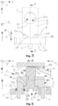
- Figure 1 shows an exemplary embodiment of a conductor connection device 1 according to the present invention mounted to a printed circuit board 2 according to the present invention in a schematic perspective view.
- the connection device 1 extends along a longitudinal direction X, a transverse direction Y, and a height direction Z, together constituting a Cartesian coordinate system.
- the conductor connection device 1 has a main body 3 with a conductor receiving opening 4 for introducing a section of a conductor into a conductor receptacle 4A in a receiving direction R.
- the conductor receptacle 4A is accessible through the conductor receiving opening 4.
- the receiving opening 4 opens against the receiving direction R in a first outer side 5 of the main body 3.
- the first outer side 5 may essentially extend perpendicular to the receiving direction R.
- the conductor connection device 1 comprises at least one contact element 6 that is adapted to electrically and/or mechanically connect the main body 3 to the printed circuit board 2.
- the contact element 6 is arranged at a second outer side 7 of the main body 3, wherein the second outer side 7 is for the most part covered by the printed circuit board 2 in the view of figure 1 .
- the second outer side 7 may differ from the first outer side 5 and may for example extend parallel to the receiving a direction R.
- the conductor connection device 1 comprises two contact elements 6.
- the two contact elements 6 may be arranged after each other in the receiving a direction R.
- the conductor connection device 1 furthermore comprises a conductor clamping element 8.
- the conductor clamping element 8 is adapted to clamp a section of the conductor within the conductor receptacle 4A, i.e. in case the conductor is arranged in the conductor receptacle 4A, wherein the conductor clamping element 8 is adapted to press the section of the conductor against an inner wall of the conductor receptacle 4A.
- the conductor connection device 1 comprises at least two contact elements 6, the conductor clamping element 8 and/or the conductor receiving opening 4 may be arranged between the at least two contact elements 6, for example along the receiving a direction R.
- the conductor clamping element 8 may be formed as an elastic clamping element with at least one latching device, and may span the main body 3.
- the conductor clamping element 8 is exemplary shown as a setscrew, grub screw or headless screw.
- the main body 3 may comprise a clamping element receptacle 9A, within which the conductor clamping element 8 is at least partly or even completely arranged in a movable manner.
- the clamping element receptacle 9A opens in the second outer side 7 with a clamping element opening 9 and extends from the clamping element opening 9 in the second outer side 7 to the conductor receptacle 4A.
- the conductor connection device 1 comprises at least two contact elements 6, the clamping element opening 9 may be arranged between the at least two contact elements 6, for example along the receiving direction R.
- the conductor clamping element 8 may be movable in and can optionally also be rotatable around a rotational axis extending essentially in parallel to a clamping direction C, which may essentially extend perpendicular to the receiving direction R, perpendicular to the second outer side 7 and/or parallel to the first outer side 5.
- the clamping element receptacle 9A may extend along the clamping direction C.
- the receiving direction R extends along the longitudinal direction X
- the clamping direction C extends along the height direction Z.
- the printed circuit board 2 may be a printed circuit board for a utility meter and comprises the conductor connection device 1.
- the printed circuit board 2 comprises a counter contact element 10, to which one of the contact elements 6 is electrically and/or mechanically connected.
- the counter contact element 10 may be a contact pad of the printed circuit board 2, which is exemplarily shown having a ring-shape surrounding a vertical interconnect access hole of the printed circuit board 2.
- the printed circuit board 2 may comprise a through-hole 11, via which the conductor clamping element 8 is accessible.
- the through-hole 11 may be aligned with the conductor clamping element 8 and/or the clamping element receptacle 9A and/or the clamping element opening 9.
- the printed circuit board 2 may comprise two counter contact elements 10, wherein the through hole 11 may be arranged between the two counter contact elements 10.
- the at least one contact element 6 surmounts the main body 3 perpendicular to the second outer side 7 and may protrude from the second outer side 7.
- the at least one contact element 6 is formed as a contact pin.
- the at least one contact element 6 may be formed as a contact pad that can be arranged on and/or be essentially flush with the second outer side 7.
- the at least one contact element 6 and the main body 3 may be adapted to be handled as a single piece.
- the at least one contact elements 6 or all of the contact elements 6 and the main body 3 may be formed out of a single piece of metal or the at least one contact element 6 or all of the contact elements 6 may be affixed to the main body 3, for example by welding or soldering.
- the at least one contact element 6 or all of the contact elements 6 are formed as contact pads, the at least one contact element 6 or all of the contact elements 6 can be coated onto the second outer side 7.
- Figure 2 shows the exemplary embodiment of the conductor connection device 1 illustrated in figure 1 in a schematic perspective view.
- a transition zone 6A protrudes from the second outer side 7 of the main body 3 in a direction opposite to the clamping direction C.
- a shoulder surface 7A is formed at the transition zone 6A and faces in the same direction as the second outer surface 7A.
- the shoulder surface 7A serves for supporting the conductor connection device 1 at the printed circuit board 2.
- the transition zone 6A is formed as a lug or projection which tapers in a direction opposite to the clamping direction C.
- Figure 3 shows the exemplary embodiment of the conductor connection device 1 illustrated in figures 1 and 2 in a schematic front view.
- the contact element 6 juts above an upper side 2A of the printed circuit board 2 in the height direction Z, i.e. in a direction opposite to the clamping direction C.
- the upper side 2B faces away from the main body 3.
- the contact element 6 is connected to the main body 3 by the transition zone 6A.
- the contact element 6 merges with the main body 3.
- the transition zone 6A has a trapezoid shape in a projection along the receiving direction R.
- the second outer side 7 of the conductor connection device 1 is distanced from the printed circuit board 2 by a distance d which is measured in parallel to the height direction Z, and/or the clamping direction C, respectively, and is essentially bridged by the transition zone 6A.
- the conductor clamping element 8 is accessible through a gap having the width of the distance d between a lower side 2B of the printed circuit board 2 and the second outer side 7 of the main body 3.
- the upper side 2A and the lower side 2B face away from each other and are opposite sides of the printed circuit board 2.
- the clamping element 8 comprises a clamping portion 8A, an actuation portion 8B, and an abutment section 8C.
- the clamping portion 8A may be arranged within the main body 3 of the conductor connection device 1, such that at least partly overlaps with the conductor receiving opening 4 and/or the conductor receptacle 4A in a projection along the receiving direction R.
- the actuation portion 8B is arranged behind the main body 3 in the height direction Z, i.e. in a direction against the clamping direction C.
- Figure 4 shows the exemplary embodiment of the conductor connection device 1 illustrated in figures 1 to 3 in a schematic cross-sectional view along a cross-sectional line A-A depicted in figure 3 , and with a conductor connected to the conductor connection device 1.
- the cross-sectional plane extends along the receiving a direction R and the clamping direction C.
- a conductor 12 is shown.
- the conductor 12 may be a line or wire.
- a bare or stripped end 13 of the conductor 12 is at least partly inserted via the receiving opening 4 into conductor receptacle 4A in the receiving direction R.
- the bare end 13 of the conductor 12 is arranged between the conductor clamping element 8, in particular a lower end of the clamping portion 8A, facing the clamping direction C, and an inner wall 14 of the main body 3.
- the inner wall 14 may be arranged behind to the clamping element opening 9A the clamping direction C and may at least sectionwise delimit the receiving opening 4 in the clamping direction C.
- the clamping portion 8A of the conductor clamping element 8 is held at an engagement portion 9B of the clamping element receptacle 9A such that it is supported in a direction opposite to the clamping direction C, for example in that the clamping portion 8A and the engagement portion 9B are threaded in a complementary manner.
- the actuation portion 8B of the conductor clamping element 8 is at least partly accommodated in a socket portion 9C of the clamping element receptacle 9A formed between the transition zones 6A.
- the abutment section 8C of the conductor clamping element 8 abuts a bottom 9D of the socket portion 9C in the clamping direction C.
- the bottom 9D is constituted by a part of the second outer surface 7.
- the abutment section 8C is e.g. formed as a shoulder or ledge at the conductor clamping element 8 and acts as a limit stop for any movement of the conductor clamping element 8 in the clamping direction C.
- a clearance between the conductor clamping element 8, in particular the clamping portion 8A thereof, and the inner wall 14 of the main body 3 may be provided for avoiding an excessive deformation of the bare end 13 of the conductor 12.
- the contact elements 6 extend through contact receptacles 10A provided within the printed circuit board 2 in the form of pin-in-holes.
- the contact receptacles 10A are dimensioned such that the counter contact elements 10 essentially fill up the circumferential space between the contact elements 6 and the contact receptacles 10A.
- the socket portion 9C is dimensioned such that the conductor clamping element 8, in particular the actuation portion 8B thereof, is embedded within a space constituted by the socket portion 9C and the through-hole 11 of the printed circuit board 2. In other words, in a clamping position S shown in Figure 4 , the conductor clamping element 8 is moved beyond the upper side 2A of the printed circuit board 2.
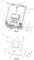
- FIG. 5 shows an exemplary embodiment of a utility meter 20 according to an embodiment of the present invention, for example for metering electricity supplied to a facility or to a home, in a pre-assembled state A.
- the utility meter 20 comprises the printed circuit board 2, wherein the conductor connection device 1 is mounted to a side of the printed circuit board 2.
- Mounting the conductor connection device 1 to the printed circuit board 2 may mean that the conductor connection device 1 is arranged on said side of the printed circuit board 2.
- the conductor connection device 1 may be affixed to the printed circuit board 2 and for example at the side it is mounted to.
- the printed circuit board 2 may have a mounting side for mounting at least selected electrical components of the utility meter 20.
- the conductor connection device 1 may be mounted to the mounting side.
- the main body 3 may be provided at the mounting side.
- the mounting side faces into a housing 21 of the utility meter 20, such that the mounting side is not visible.
- the printed circuit board 2, when arranged in the housing 21, may comprise an operation side 22 that faces out of the housing 21 and in particular faces a user or an installer of the utility meter 20.
- the upper side 2A of the printed circuit board 2 is designated as the operation side 22.
- the conductor clamping element 8 is accessible through the through-hole 11 via the operation side 22, i.e. the upper side 2A of the printed circuit board 2.
- additional components for example of a user interface comprising a display 23 and buttons 24 are arranged on the operation side 22 of the printed circuit board 2.
- the housing 21 comprises a front opening 25 that opens the housing 21 towards a user or an installer, such that the user or installer can access the printed circuit board 2 in the clamping direction C via the front opening 25.
- the operation side 22 faces the user through the front opening 25.
- the front opening 25 may extend perpendicular to the clamping direction C.
- the housing 21 may comprise a connection opening 26 for connecting the utility meter 21 to the conductor 12 via the connection opening 26.
- the conductor receiving opening 4 may face the connection opening 26.
- the connection opening 26 may extend perpendicular to the receiving direction R.
- the front opening 25 and the connection opening 26 may be formed continuously.
- Figure 6 shows the utility meter 20 of the exemplary embodiment shown in figure 5 in a fully assembled state B, in which the housing 21 of the utility meter 20 is closed by a lid 27.
- the lid 27 may be adapted to close the front opening 25 of the housing 21 that faces away from the mounting side of the printed circuit board 2. Additionally, the lid 27 may be adapted to close the connection opening 26 in the completely assembles state of the utility meter 20.
- the conductor connection device 1 and the printed circuit board 2 may be formed as required for connecting a conductor 12, such as a line, cable, wire, or alike, to the printed circuit board 2.
- the conductor connection device 1 may therefore comprise a main body 3 with conductor receiving openings 4, conductor receptacles 4A, first outer side 5, contact elements 6, transition zones 6A, second outer sides 7, shoulder surfaces 7A, conductor clamping elements 8 with clamping portions 8A, actuation portions 8B and/or abutment sections 8C, clamping element openings 9 to clamping element receptacles 9A, comprising engagement portions 9B, socket portions 9C, and/or bottoms 9D, inner walls 14, in any number and form required for connecting a conductor 12 to the printed circuit board 2 in line with the present invention.
- the printed circuit board 2 may therefore analogously comprise upper sides 2A, lower sides 2B, counter contact elements 10, contact receptacles 10A, through-holes 11, and/or operation side 22 and any number and form required for supporting and mounting a conductor connection device 1 for connecting a conductor 12 to the printed circuit board tool in line with the present invention.
- the utility meter 20 may comprise conductor connection devices 1, printed circuit boards 2, housings 21, displays 23, buttons 24, front openings 25, connection openings 26, and/or lids 27 and any number and form required.
Landscapes
- Physics & Mathematics (AREA)
- General Physics & Mathematics (AREA)
- Engineering & Computer Science (AREA)
- Power Engineering (AREA)
- Coupling Device And Connection With Printed Circuit (AREA)
Description
- The present invention relates to a conductor connection device for connecting an electrical conductor to a printed circuit board, comprising a main body having a conductor receptacle accessible through a conductor receiving opening for inserting a section of a conductor, for example a line or wire, into the conductor receptacle, the conductor receiving opening being arranged at a first outer side of the main body, a contact element in the form of a contact pin adapted to electrically and mechanically connect the main body to a printed circuit board, the contact element being arranged at a second outer side of the main body, and a conductor clamping element adapted to clamp a section of the conductor within the conductor receptacle, wherein the conductor clamping element is accessible, i.e. operable, via the second outer side of the main body.
- Furthermore, the invention relates to a printed circuit board for a utility meter, comprising a conductor connection device.
- Moreover, the invention relates to a utility meter comprising a conductor connection device and/or a printed circuit board.
- Utility meters, for example electricity meters, are known from the prior art and serve for determining the amount of consumption of a medium, like water or gas, or of electrical energy supplied. In order to connect the utility meter to a power supply or to a source of electrical energy to be supplied and metered, the utility meter comprises the conductor connection device.
- For instance,
WO 98/10299 A1 FR 2 667 990 A1DE 10 2014 103562 A1 relate to connection clamps to be mounted to a PCB and having contact elements for electrically contacting the PCB which are arranged at the same sides as actuation openings for accessing conductor clamping elements. - Conductor connection devices are commonly used to electrically connect an electrical conductor, e.g. a line or a wire, to an apparatus and for example to a utility meter. Conductor connection devices need to be cheap and in particular are meant to facilitate making the connection to the conductor. In use, conductor connection devices conduct electricity and need to comprise an insulating housing to protect users, for example operators or installers of the utility meter, from the electricity. However, due to the requirements to the housing, known conductor connection devices are expensive to mount and manufacture.
- It is an object of the present invention, to at least partly mitigate some of the above-mentioned disadvantages of utility meters and their conductor connection devices known from the prior art. In particular, an object underlying the invention is to provide a conductor connection device that can be manufactured and mounted at reasonable costs without compromising electrical safety of the utility meter.
- For the above-mentioned conductor connection device, the object is achieved according to the present invention in that the conductor connection device comprises: a main body having a conductor receptacle accessible through a conductor receiving opening for inserting a section of the conductor into the conductor receptacle, the conductor receiving opening being arranged at a first outer side of the main body, a contact element in the form of a contact pin adapted to electrically and mechanically connect the main body to a printed circuit board, the contact element being arranged at a second outer side of the main body, and a conductor clamping element adapted to clamp the section of the conductor in a clamping direction within the conductor receptacle, wherein the conductor clamping element is accessible via the second outer side of the main body, characterised in that: a transition zone protrudes from the second outer side of the main body in a direction opposite to the clamping direction; a shoulder surface is formed at the transition zone and faces in the same direction as the second outer surface, the shoulder surface serves for supporting the conductor connection device at the printed circuit board; the transition zone is formed as a lug or projection which tapers in a direction opposite to the clamping direction; and both the contact element and a small platform or step, a flat top of which essentially constitutes the shoulder surface, protrude from the transition zone in parallel to each other in a direction opposite to the clamping direction.. The object is achieved according to the invention for the printed circuit board in that the conductor connection device is a conductor connection device according to the present invention. Furthermore, the object is achieved according to the present invention for the utility meter in that the conductor connection device is a conductor connection device according to the invention and/or the printed circuit board is a printed circuit board according to the invention.
- Due to the accessibility of the clamping element via the second outer side, which also comprises the contact element, a user of the conductor connection device can readily operate the conductor clamping device from the second outer side that faces the printed circuit board. Hence, the printed circuit board can separate the user from the conductor connection device and may, thus, act as an insulating element that prevents physical contact between the user and the conductor connection device, such that an additional housing for the conductor connection device may not be required.
- Unless explicitly stated to the contrary, the solutions according to the invention can be combined as desired and further improved by the further following embodiments that are advantages on their own, in each case.
- According to a possible embodiment, the first outer side differs from the second outer side. An advantage of this embodiment may be that different functions of the conductor connection device are accessible from different sides, i.e. the receiving function of the conductor receptacle is accessible from the first outer side, whereas the operating function of the conductor clamping element is accessible from the second outer side.
- According to a possible embodiment, the main body further comprises a clamping element receptacle in which the conductor clamping element is arranged in a movable manner, wherein the clamping element receptacle at least partly intersects the conductor receptacle. An advantage of this embodiment may be that the clamping element receptacle may guide the movement of the clamping element.
- According to a possible embodiment, the clamping element receptacle has a clamping element opening arranged at the second outer side. An advantage of this embodiment may be that the clamping element is readily accessible via the clamping element opening at the second outer side.
- According to another possible embodiment, the conductor receptacle and the clamping element receptacle together at least partly define an inner space of the main body, which inner space extends from the second outer side to the conductor receiving opening. An advantage of this embodiment may be that due to the continuous inner space formed by the conductor receptacle and the clamping element receptacle, the conductor and the conductor clamping element can be readily brought into positions, in which a projection of the conductor clamping element along the clamping element receptacle overlaps the conductor in the conductor receptacle, such that the conductor clamping element merely needs to be moved along the clamping element receptacle in order to simply clamp the conductor.
- According to another possible embodiment, the contact element surmounts the main body perpendicular to the second outer side. The contact element may be affixed to the second outer side or to another outer side of the main body and may extend perpendicular to the second outer side with its free end facing away from the main body. For example, the contact element may protrude from the second outer side. An advantage of this embodiment may be that the contact element may be formed as a contact pin, which can easily be connected to another conductor or to an electronic device like the printed circuit board, for example by soldering. Alternatively, the contact element may be a contact pad arranged on the second outer side.
- According to another possible embodiment, the contact element and the main body and optionally also the clamping element are adapted to be handled as a single piece. An advantage of this embodiment may be that the conductor connection device can be handled and mounted easily.
- According to another possible embodiment, the conductor connection device comprises at least two contact elements arranged at the second outer side, wherein the conductor clamping element is arranged between the two contact elements. An advantage of this embodiment may be that the arrangement of the clamping element between the contact elements improves absorption of forces that seek to move the main body when operating, i.e. moving, the clamping element, in particular in case the contact elements not only conductively connect, but also mechanically affix the conductor connection device to another electronic device, e.g. the printed circuit board.
- According to another possible embodiment, the contact element is embodied as a stud or peg. An advantage of this embodiment may be that the conductor connection device can easily be connected to a counter contact element, wherein the contact element defines the position of the conductor connection device, in particular if the counter contact element is at least partly formed complementary to the contact element.
- According to another possible embodiment, the contact element is adapted to be soldered to the printed circuit board and/or a component thereof. An advantage of this embodiment may be that the conductor connection device can easily be mounted and at the same time electrically connected to the printed circuit board.
- According to another possible embodiment, the clamping element is embodied as a setscrew or grub screw. An advantage of this embodiment may be that in order to clamp the conductor, the clamping element can simply be screwed in the clamping element receptacle. Furthermore, clamping forces that clamp the conductor result in counterforces that act on the thread of the setscrew or grub screw and a counter thread that may be formed by the clamping element receptacle, which counterforces prevent that the setscrew or grub screw loosens the force-fit screw connection and, hence, secure that force fit by which the conductor is clamped.
- According to a possible embodiment of the printed circuit board, the conductor connection device is mounted to the printed circuit board, such that a contact element of the conductor connection device is electrically connected to a counter contact element of the printed circuit board, wherein the printed circuit board comprises a through-hole that is essentially aligned with the conductor clamping element for accessing the conductor clamping element via the though-hole. An advantage of this embodiment may be that although the conductor connection device is arranged on one side of the printed circuit board, the clamping element is readily accessible via the through-hole from the opposite side of the printed circuit board, thereby effectively preventing unintended contact between the conductor connection device and the user.
- According to a possible embodiment of the printed circuit board, the printed circuit board comprises at least two counter contact elements, wherein the through-hole is arranged between the two counter contact elements. An advantage of this embodiment may be that the arrangement of the through-hole between the counter contact elements improves absorption of forces that seek to move the main body when operating, i.e. moving, the clamping element.
- According to a possible embodiment of the utility meter, the printed circuit board comprises a mounting side for mounting at least selected electrical components of the utility meter, and an operation side that faces a user of the utility meter, the mounting side and the operating side facing away from each other, wherein the conductor connection device is mounted to the mounting side and the conductor clamping element is accessible through the through access hole via the operation side. An advantage of this embodiment may be that the printed circuit board prevents or at least impedes direct contact of a user to the conductor connection device, which improves operational safety of the utility meter.
- The invention will be described hereinafter in more detail and in an exemplary manner using advantageous embodiments and with reference to the drawings. The described embodiments are only possible configurations in which, however, the individual features as described above can be provided independent of one another or can be omitted in the drawings:
- Figure 1
- shows an exemplary embodiment of a conductor connection device according to the present invention mounted to an exemplary embodiment of a printed circuit board according to the present invention in a schematic perspective view,
- Figure 2
- shows the exemplary embodiment of the conductor connection device illustrated in
figure 1 in a schematic perspective view, - Figure 3
- shows the exemplary embodiment of the conductor connection device illustrated in
figures 1 and2 in a schematic front view, - Figure 4
- shows the exemplary embodiment of the conductor connection device illustrated in
figures 1 to 3 in a schematic cross-sectional view along the cross-sectional line A-A depicted inFigure 3 , - Figure 5
- shows an exemplary embodiment of a utility meter according to the present invention in a schematic perspective view in a pre-assembled state, and
- Figure 6
- shows the utility meter illustrated in
figure 5 in a fully assembled state. -
Figure 1 shows an exemplary embodiment of a conductor connection device 1 according to the present invention mounted to a printedcircuit board 2 according to the present invention in a schematic perspective view. The connection device 1 extends along a longitudinal direction X, a transverse direction Y, and a height direction Z, together constituting a Cartesian coordinate system. The conductor connection device 1 has amain body 3 with aconductor receiving opening 4 for introducing a section of a conductor into aconductor receptacle 4A in a receiving direction R. Hence, theconductor receptacle 4A is accessible through theconductor receiving opening 4. The receivingopening 4 opens against the receiving direction R in a firstouter side 5 of themain body 3. The firstouter side 5 may essentially extend perpendicular to the receiving direction R. - The conductor connection device 1 comprises at least one
contact element 6 that is adapted to electrically and/or mechanically connect themain body 3 to the printedcircuit board 2. Thecontact element 6 is arranged at a secondouter side 7 of themain body 3, wherein the secondouter side 7 is for the most part covered by the printedcircuit board 2 in the view offigure 1 . The secondouter side 7 may differ from the firstouter side 5 and may for example extend parallel to the receiving a direction R. In the exemplary embodiment offigure 1 , the conductor connection device 1 comprises twocontact elements 6. The twocontact elements 6 may be arranged after each other in the receiving a direction R. - The conductor connection device 1 furthermore comprises a
conductor clamping element 8. Theconductor clamping element 8 is adapted to clamp a section of the conductor within theconductor receptacle 4A, i.e. in case the conductor is arranged in theconductor receptacle 4A, wherein theconductor clamping element 8 is adapted to press the section of the conductor against an inner wall of theconductor receptacle 4A. In case the conductor connection device 1 comprises at least twocontact elements 6, theconductor clamping element 8 and/or theconductor receiving opening 4 may be arranged between the at least twocontact elements 6, for example along the receiving a direction R. - For example, the
conductor clamping element 8 may be formed as an elastic clamping element with at least one latching device, and may span themain body 3. However, infigure 1 , theconductor clamping element 8 is exemplary shown as a setscrew, grub screw or headless screw. - In particular if the
conductor clamping element 8 is a setscrew or headless screw, but also if theconductor clamping element 8 is formed differently and for example as the elastic clamping element with the at least one latching device, themain body 3 may comprise a clamping element receptacle 9A, within which theconductor clamping element 8 is at least partly or even completely arranged in a movable manner. The clamping element receptacle 9A opens in the secondouter side 7 with a clamping element opening 9 and extends from the clamping element opening 9 in the secondouter side 7 to theconductor receptacle 4A. If the conductor connection device 1 comprises at least twocontact elements 6, the clamping element opening 9 may be arranged between the at least twocontact elements 6, for example along the receiving direction R. - In particular, the
conductor clamping element 8 may be movable in and can optionally also be rotatable around a rotational axis extending essentially in parallel to a clamping direction C, which may essentially extend perpendicular to the receiving direction R, perpendicular to the secondouter side 7 and/or parallel to the firstouter side 5. For example, in order to move theconductor clamping element 8 in the clamping direction C, the clamping element receptacle 9A may extend along the clamping direction C. In the present embodiment, the receiving direction R extends along the longitudinal direction X, and the clamping direction C extends along the height direction Z. - The printed
circuit board 2 may be a printed circuit board for a utility meter and comprises the conductor connection device 1. For example, the printedcircuit board 2 comprises acounter contact element 10, to which one of thecontact elements 6 is electrically and/or mechanically connected. Thecounter contact element 10 may be a contact pad of the printedcircuit board 2, which is exemplarily shown having a ring-shape surrounding a vertical interconnect access hole of the printedcircuit board 2. - The printed
circuit board 2 may comprise a through-hole 11, via which theconductor clamping element 8 is accessible. The through-hole 11 may be aligned with theconductor clamping element 8 and/or the clamping element receptacle 9A and/or the clamping element opening 9. The printedcircuit board 2 may comprise twocounter contact elements 10, wherein the through hole 11 may be arranged between the twocounter contact elements 10. - In the exemplary embodiment of
figure 1 , the at least onecontact element 6 surmounts themain body 3 perpendicular to the secondouter side 7 and may protrude from the secondouter side 7. For example, the at least onecontact element 6 is formed as a contact pin. Alternatively, the at least onecontact element 6 may be formed as a contact pad that can be arranged on and/or be essentially flush with the secondouter side 7. - The at least one
contact element 6 and themain body 3 may be adapted to be handled as a single piece. For example, the at least onecontact elements 6 or all of thecontact elements 6 and themain body 3 may be formed out of a single piece of metal or the at least onecontact element 6 or all of thecontact elements 6 may be affixed to themain body 3, for example by welding or soldering. In case the at least onecontact element 6 or all of thecontact elements 6 are formed as contact pads, the at least onecontact element 6 or all of thecontact elements 6 can be coated onto the secondouter side 7. -
Figure 2 shows the exemplary embodiment of the conductor connection device 1 illustrated infigure 1 in a schematic perspective view. Here it becomes apparent that a transition zone 6A protrudes from the secondouter side 7 of themain body 3 in a direction opposite to the clamping direction C. A shoulder surface 7A is formed at the transition zone 6A and faces in the same direction as the second outer surface 7A. The shoulder surface 7A serves for supporting the conductor connection device 1 at the printedcircuit board 2. According to the present exemplary embodiment, the transition zone 6A is formed as a lug or projection which tapers in a direction opposite to the clamping direction C. Both, thecontact element 6 and a small platform orstep 7B, a flat top of which essentially constitutes the shoulder surface 7A, protrude from the transition zone 6A in parallel to each other in a direction opposite to the clamping direction C. -
Figure 3 shows the exemplary embodiment of the conductor connection device 1 illustrated infigures 1 and2 in a schematic front view. Here it becomes apparent that thecontact element 6 juts above an upper side 2A of the printedcircuit board 2 in the height direction Z, i.e. in a direction opposite to the clamping direction C. The upper side 2B faces away from themain body 3. Thecontact element 6 is connected to themain body 3 by the transition zone 6A. In the transition zone 6A, thecontact element 6 merges with themain body 3. The transition zone 6A has a trapezoid shape in a projection along the receiving direction R. The secondouter side 7 of the conductor connection device 1 is distanced from the printedcircuit board 2 by a distance d which is measured in parallel to the height direction Z, and/or the clamping direction C, respectively, and is essentially bridged by the transition zone 6A. - The
conductor clamping element 8 is accessible through a gap having the width of the distance d between a lower side 2B of the printedcircuit board 2 and the secondouter side 7 of themain body 3. The upper side 2A and the lower side 2B face away from each other and are opposite sides of the printedcircuit board 2. The clampingelement 8 comprises a clampingportion 8A, an actuation portion 8B, and an abutment section 8C. The clampingportion 8A may be arranged within themain body 3 of the conductor connection device 1, such that at least partly overlaps with theconductor receiving opening 4 and/or theconductor receptacle 4A in a projection along the receiving direction R. The actuation portion 8B is arranged behind themain body 3 in the height direction Z, i.e. in a direction against the clamping direction C. -
Figure 4 shows the exemplary embodiment of the conductor connection device 1 illustrated infigures 1 to 3 in a schematic cross-sectional view along a cross-sectional line A-A depicted infigure 3 , and with a conductor connected to the conductor connection device 1. The cross-sectional plane extends along the receiving a direction R and the clamping direction C. In addition to the conductor connection device 1, a conductor 12 is shown. The conductor 12 may be a line or wire. A bare or stripped end 13 of the conductor 12 is at least partly inserted via the receivingopening 4 intoconductor receptacle 4A in the receiving direction R. In the clamping direction C, the bare end 13 of the conductor 12 is arranged between theconductor clamping element 8, in particular a lower end of the clampingportion 8A, facing the clamping direction C, and aninner wall 14 of themain body 3. Theinner wall 14 may be arranged behind to the clamping element opening 9A the clamping direction C and may at least sectionwise delimit the receivingopening 4 in the clamping direction C. - The clamping
portion 8A of theconductor clamping element 8 is held at an engagement portion 9B of the clamping element receptacle 9A such that it is supported in a direction opposite to the clamping direction C, for example in that the clampingportion 8A and the engagement portion 9B are threaded in a complementary manner. The actuation portion 8B of theconductor clamping element 8 is at least partly accommodated in a socket portion 9C of the clamping element receptacle 9A formed between the transition zones 6A. The abutment section 8C of theconductor clamping element 8 abuts a bottom 9D of the socket portion 9C in the clamping direction C. According to the present exemplary embodiment, the bottom 9D is constituted by a part of the secondouter surface 7. The abutment section 8C is e.g. formed as a shoulder or ledge at theconductor clamping element 8 and acts as a limit stop for any movement of theconductor clamping element 8 in the clamping direction C. Thereby, a clearance between theconductor clamping element 8, in particular the clampingportion 8A thereof, and theinner wall 14 of themain body 3 may be provided for avoiding an excessive deformation of the bare end 13 of the conductor 12. - Furthermore, the
main body 3, in particular the shoulder surface 7A thereof, rests on the lower side 2B of the printedcircuit board 2. While the conductor connection device 1 is thus supported on the printedcircuit board 2, thecontact elements 6 extend through contact receptacles 10A provided within the printedcircuit board 2 in the form of pin-in-holes. The contact receptacles 10A are dimensioned such that thecounter contact elements 10 essentially fill up the circumferential space between thecontact elements 6 and the contact receptacles 10A. The socket portion 9C is dimensioned such that theconductor clamping element 8, in particular the actuation portion 8B thereof, is embedded within a space constituted by the socket portion 9C and the through-hole 11 of the printedcircuit board 2. In other words, in a clamping position S shown inFigure 4 , theconductor clamping element 8 is moved beyond the upper side 2A of the printedcircuit board 2. -
Figure 5 shows an exemplary embodiment of autility meter 20 according to an embodiment of the present invention, for example for metering electricity supplied to a facility or to a home, in a pre-assembled state A. Theutility meter 20 comprises the printedcircuit board 2, wherein the conductor connection device 1 is mounted to a side of the printedcircuit board 2. Mounting the conductor connection device 1 to the printedcircuit board 2 may mean that the conductor connection device 1 is arranged on said side of the printedcircuit board 2. The conductor connection device 1 may be affixed to the printedcircuit board 2 and for example at the side it is mounted to. - The printed
circuit board 2 may have a mounting side for mounting at least selected electrical components of theutility meter 20. The conductor connection device 1 may be mounted to the mounting side. In particular, themain body 3 may be provided at the mounting side. In the exemplary embodiment shown infigure 5 , the mounting side faces into ahousing 21 of theutility meter 20, such that the mounting side is not visible. Furthermore, the printedcircuit board 2, when arranged in thehousing 21, may comprise an operation side 22 that faces out of thehousing 21 and in particular faces a user or an installer of theutility meter 20. In the present embodiment, the upper side 2A of the printedcircuit board 2 is designated as the operation side 22. Theconductor clamping element 8 is accessible through the through-hole 11 via the operation side 22, i.e. the upper side 2A of the printedcircuit board 2. - In the exemplary embodiment shown in
figure 5 , additional components, for example of a user interface comprising adisplay 23 andbuttons 24 are arranged on the operation side 22 of the printedcircuit board 2. Thehousing 21 comprises afront opening 25 that opens thehousing 21 towards a user or an installer, such that the user or installer can access the printedcircuit board 2 in the clamping direction C via thefront opening 25. The operation side 22 faces the user through thefront opening 25. Hence, thefront opening 25 may extend perpendicular to the clamping direction C. Additionally or alternatively, thehousing 21 may comprise aconnection opening 26 for connecting theutility meter 21 to the conductor 12 via theconnection opening 26. Theconductor receiving opening 4 may face theconnection opening 26. Thus, theconnection opening 26 may extend perpendicular to the receiving direction R. Thefront opening 25 and theconnection opening 26 may be formed continuously. -
Figure 6 shows theutility meter 20 of the exemplary embodiment shown infigure 5 in a fully assembled state B, in which thehousing 21 of theutility meter 20 is closed by a lid 27. The lid 27 may be adapted to close thefront opening 25 of thehousing 21 that faces away from the mounting side of the printedcircuit board 2. Additionally, the lid 27 may be adapted to close theconnection opening 26 in the completely assembles state of theutility meter 20. - The conductor connection device 1 and the printed
circuit board 2 may be formed as required for connecting a conductor 12, such as a line, cable, wire, or alike, to the printedcircuit board 2. - The conductor connection device 1 may therefore comprise a
main body 3 withconductor receiving openings 4,conductor receptacles 4A, firstouter side 5,contact elements 6, transition zones 6A, secondouter sides 7, shoulder surfaces 7A,conductor clamping elements 8 with clampingportions 8A, actuation portions 8B and/or abutment sections 8C, clamping element openings 9 to clamping element receptacles 9A, comprising engagement portions 9B, socket portions 9C, and/or bottoms 9D,inner walls 14, in any number and form required for connecting a conductor 12 to the printedcircuit board 2 in line with the present invention. - The printed
circuit board 2 may therefore analogously comprise upper sides 2A, lower sides 2B,counter contact elements 10, contact receptacles 10A, through-holes 11, and/or operation side 22 and any number and form required for supporting and mounting a conductor connection device 1 for connecting a conductor 12 to the printed circuit board tool in line with the present invention. Theutility meter 20 may comprise conductor connection devices 1, printedcircuit boards 2,housings 21, displays 23,buttons 24,front openings 25,connection openings 26, and/or lids 27 and any number and form required. -
- 1
- conductor connection device
- 2
- printed circuit board
- 2A
- upper side
- 2B
- lower side
- 3
- main body
- 4
- conductor receiving opening
- 4A
- conductor receptacle
- 5
- first outer side
- 6
- contact element
- 6A
- transition zone
- 7
- second outer side
- 7A
- shoulder surface
- 7B
- step
- 8
- conductor clamping element
- 8A
- clamping portion
- 8B
- actuation portion
- 8C
- abutment section
- 9
- clamping element opening
- 9A
- clamping element receptacle
- 9B
- engagement portion
- 9C
- socket portion
- 9D
- bottom
- 10
- counter contact elements of the printed circuit board
- 10A
- contact receptacle
- 11
- through-hole of printed circuit board
- 12
- conductor
- 13
- bare end of conductor
- 14
- inner wall of the main body
- 20
- utility meter
- 21
- housing of utility meter
- 22
- operation side
- 23
- display
- 24
- button
- 25
- front opening
- 26
- connection opening
- 27
- lid
- d
- distance between second outer side and printed circuit board
- A
- pre-assembled state
- B
- fully assembled state
- C
- clamping direction
- R
- receiving direction
- S
- Clamping position
- X
- longitudinal direction
- Y
- transverse direction
- Z
- height direction
Claims (15)
- Conductor connection device (1) for connecting an electrical conductor (12) to a printed circuit board (2), comprisinga main body (3) having a conductor receptacle (4A) accessible through a conductor receiving opening (4) for inserting a section (13) of the conductor (12) into the conductor receptacle (4A), the conductor receiving opening (4) being arranged at a first outer side (5) of the main body (3),a contact element (6) in the form of a contact pin adapted to electrically and mechanically connect the main body (3) to a printed circuit board (2), the contact element (6) being arranged at a second outer side (7) of the main body (3), anda conductor clamping element (8) adapted to clamp the section (13) of the conductor (12) in a clamping direction (C) within the conductor receptacle (4A), whereinthe conductor clamping element (8) is accessible via the second outer side (7) of the main body (3),characterised in that:a transition zone (6A) protrudes from the second outer side (7) of the main body (3) in a direction opposite to the clamping direction (C);a shoulder surface (7A) is formed at the transition zone (6A) and faces in the same direction as the second outer surface (7), the shoulder surface (7A) serves for supporting the conductor connection device (1) at the printed circuit board (2);the transition zone (6A) is formed as a lug or projection which tapers in a direction opposite to the clamping direction (C); andboth the contact element (6) and a small platform or step (7B), a flat top of which essentially constitutes the shoulder surface (7A), protrude from the transition zone (6A) in parallel to each other in a direction opposite to the clamping direction (C).
- Conductor connection device (1) according to claim 1, characterised in that the main body (3) further comprises a clamping element receptacle (9A) in which the conductor clamping element (8) is arranged in a movable manner, wherein the clamping element receptacle (9A) at least partly intersects the conductor receptacle (4A).
- Conductor connection device (1) according to claim 2, characterised in that the clamping element receptacle (9A) has a clamping element opening (9) arranged at the second outer side (7).
- Conductor connection device (1) according to claim 2 or 3, characterised in that the conductor receptacle (4A) and the clamping element receptacle (9A) together at least partly define an inner space of the main body (3), which inner space extends from the second outer side (7) to the conductor receiving opening (4).
- Conductor connection device (1) according to any of claims 1 to 4, characterised in that the contact element (6) surmounts the main body (3) perpendicular to the second outer side (7).
- Conductor connection device (1) according to any of claims 1 to 5, characterised in that the contact element (6) and the main body (3) are formed out of a single piece of metal or the contact element (6) is affixed to the main body (3) such that they are adapted to be handled as a single piece.
- Conductor connection device (1) according to any of claims 1 to 6, characterised in that the conductor connection device (1) comprises at least two contact elements (6) arranged at the second outer side (7), wherein the conductor clamping element (8) is arranged between the two contact elements (6).
- Conductor connection device (1) according to any of claims 1 to 7, characterised in that the contact element (6) is embodied as a stud or peg.
- Conductor connection device (1) according to any of claims 1 to 8, characterised in that the contact element (6) is adapted to be soldered to the printed circuit board (2) and/or a component thereof.
- Conductor connection device (1) according to any of claims 1 to 9, characterised in that the clamping element (8) is embodied as a setscrew or grub screw.
- Printed circuit board (2) for a utility meter (20), comprising a conductor connection device (1) according to any of claims 1 to 10 above.
- Printed circuit board (2) according to claim 11, characterised in that the conductor connection device (1) is mounted to the printed circuit board (2), such that a contact element (6) of the conductor connection device (1) is electrically connected to a counter contact element (10) of the printed circuit board (2), wherein the printed circuit board (2) comprises a through hole (11) for accessing the conductor clamping element (8), the through hole (11) being essentially aligned with the conductor clamping element (8).
- Printed circuit board (2) according to claims 11 or 12, characterised in that the printed circuit board (2) comprises at least two counter contact elements (10), wherein the through hole (11) is arranged between the two counter contact elements (10).
- Utility meter (20) comprising a conductor connection device (1) according to any of claims 1 to 10 or a printed circuit board (2) according to any of claim 11 to 13.
- Utility meter (20) according to claim 14, characterised in that the printed circuit board (2) comprises a mounting side for mounting at least selected electrical components of the utility meter (20), and an operation side (22) that faces a user of the utility meter (20), the mounting side and the operation side (22) facing away from each other, wherein the conductor connection device (1) is mounted to the mounting side and the conductor clamping element (8) is accessible through the through access hole (11) via the operation side (22).
Applications Claiming Priority (2)
| Application Number | Priority Date | Filing Date | Title |
|---|---|---|---|
| CH00724/18A CH715072A1 (en) | 2018-06-06 | 2018-06-06 | Conductor connection device and circuit board and this comprehensive consumption meter. |
| PCT/IB2019/054402 WO2019234550A1 (en) | 2018-06-06 | 2019-05-28 | Conductor connection device as well as printed circuit board and utility meter comprising same |
Publications (2)
| Publication Number | Publication Date |
|---|---|
| EP3804037A1 EP3804037A1 (en) | 2021-04-14 |
| EP3804037B1 true EP3804037B1 (en) | 2025-03-05 |
Family
ID=63168218
Family Applications (1)
| Application Number | Title | Priority Date | Filing Date |
|---|---|---|---|
| EP19740057.5A Active EP3804037B1 (en) | 2018-06-06 | 2019-05-28 | Conductor connection device as well as printed circuit board and utility meter comprising same |
Country Status (5)
| Country | Link |
|---|---|
| US (2) | US11394144B2 (en) |
| EP (1) | EP3804037B1 (en) |
| CN (1) | CN112236904B (en) |
| CH (1) | CH715072A1 (en) |
| WO (1) | WO2019234550A1 (en) |
Citations (1)
| Publication number | Priority date | Publication date | Assignee | Title |
|---|---|---|---|---|
| WO2009082734A1 (en) * | 2007-12-20 | 2009-07-02 | Molex Incorporated | Anti-wicking terminal and connector |
Family Cites Families (25)
| Publication number | Priority date | Publication date | Assignee | Title |
|---|---|---|---|---|
| DE2500141A1 (en) * | 1974-01-23 | 1975-07-24 | Gen Signal Corp | ELECTRICAL CONNECTOR WITH VARIABLE LENGTH |
| FR2667990B1 (en) * | 1990-10-16 | 1994-07-29 | Legrand Sa | CONNECTION TERMINAL FOR A PRINTED CIRCUIT, AND PRINTED CIRCUIT EQUIPPED WITH AT LEAST ONE SUCH CONNECTION TERMINAL. |
| EP0519196B1 (en) * | 1991-06-14 | 1995-09-13 | Molex Incorporated | A terminal block for printed circuit boards |
| JP3346578B2 (en) * | 1996-09-06 | 2002-11-18 | イノヴァテック コーポレイション | Automatic meter reading data communication system |
| US20080129538A1 (en) * | 1999-02-23 | 2008-06-05 | Raj Vaswani | Electronic electric meter for networked meter reading |
| CA2305615C (en) * | 1997-10-30 | 2004-07-20 | Ekstrom Industries, Inc. | Watthour meter socket adapter |
| JP2002280700A (en) * | 2001-03-19 | 2002-09-27 | Densei Lambda Kk | Terminal structure of electronic device |
| US20060010997A1 (en) * | 2001-09-21 | 2006-01-19 | M&Fc Holding, Llc | Weather resistant automatic meter reading unit |
| US20050174708A1 (en) * | 2002-09-30 | 2005-08-11 | Price Linda G.K. | Device and method for providing electric service |
| US7074054B2 (en) * | 2004-08-06 | 2006-07-11 | Honeywell International Inc. | SMT terminal block |
| DE102006014646B4 (en) * | 2006-03-28 | 2008-06-26 | Phoenix Contact Gmbh & Co. Kg | Terminal for printed circuit boards |
| DE102007004545B4 (en) * | 2007-01-24 | 2009-01-08 | Mc Technology Gmbh | Electrical connection terminal |
| US20100081341A1 (en) * | 2008-09-30 | 2010-04-01 | Shang Tsai Wu | Pcb terminal block |
| DE102009019699B4 (en) * | 2009-05-05 | 2015-03-12 | Phoenix Contact Gmbh & Co. Kg | Terminal for printed circuit boards |
| US8105118B2 (en) * | 2009-10-22 | 2012-01-31 | Illinois Tool Works Inc. | Torque resistant terminal block element |
| CN202172147U (en) * | 2011-07-06 | 2012-03-21 | 陈太汯 | Radio frequency connector for printed circuit board |
| AT13582U1 (en) * | 2012-07-27 | 2014-04-15 | Tridonic Connection Technology Gmbh & Co Kg | Connection or connection terminal, as well as circuit board and luminaire |
| CN203013974U (en) * | 2012-08-09 | 2013-06-19 | 泰科电子(上海)有限公司 | Central terminal for electric connector and electric connector comprising same |
| CN203037704U (en) * | 2013-01-14 | 2013-07-03 | 温州市正超仪表科技有限公司 | Novel electric meter box |
| CN203644986U (en) * | 2013-12-09 | 2014-06-11 | 宁波云控电气有限公司 | Connecting structure for printed circuit board and binding post |
| DE102014103562A1 (en) * | 2014-03-14 | 2015-09-17 | Phoenix Contact Gmbh & Co. Kg | PCB submarining terminal |
| CN204257861U (en) * | 2014-07-28 | 2015-04-08 | 宁波港普光电科技有限公司 | Compact binding post |
| BE1025936B1 (en) * | 2018-01-22 | 2019-08-21 | Phoenix Contact Gmbh & Co Kg | Modular system for manufacturing an electrical device |
| LT3550272T (en) * | 2018-04-05 | 2021-05-25 | Kamstrup A/S | Compact ultrasonic flowmeter |
| US10312606B1 (en) * | 2018-07-18 | 2019-06-04 | Dinkle Enterprise Co., Ltd. | Cable fastening terminal block |
-
2018
- 2018-06-06 CH CH00724/18A patent/CH715072A1/en unknown
-
2019
- 2019-05-28 EP EP19740057.5A patent/EP3804037B1/en active Active
- 2019-05-28 CN CN201980038090.4A patent/CN112236904B/en active Active
- 2019-05-28 US US16/972,206 patent/US11394144B2/en active Active
- 2019-05-28 WO PCT/IB2019/054402 patent/WO2019234550A1/en not_active Ceased
-
2022
- 2022-06-14 US US17/839,893 patent/US12166303B2/en active Active
Patent Citations (1)
| Publication number | Priority date | Publication date | Assignee | Title |
|---|---|---|---|---|
| WO2009082734A1 (en) * | 2007-12-20 | 2009-07-02 | Molex Incorporated | Anti-wicking terminal and connector |
Also Published As
| Publication number | Publication date |
|---|---|
| US20220352661A1 (en) | 2022-11-03 |
| WO2019234550A1 (en) | 2019-12-12 |
| CH715072A1 (en) | 2019-12-13 |
| US12166303B2 (en) | 2024-12-10 |
| US11394144B2 (en) | 2022-07-19 |
| EP3804037A1 (en) | 2021-04-14 |
| CN112236904B (en) | 2023-11-21 |
| CN112236904A (en) | 2021-01-15 |
| US20210328372A1 (en) | 2021-10-21 |
Similar Documents
| Publication | Publication Date | Title |
|---|---|---|
| US7722365B2 (en) | Connector and electronic control apparatus having the same | |
| EP2109352B1 (en) | Shield case and circuit board assembly | |
| US7575443B2 (en) | Combined fastening and contacting system for electrical components on superimposed circuit boards | |
| CN102571360B (en) | A kind of networking component including electric installation | |
| EP1986478B1 (en) | Metal wiring plate | |
| US12166303B2 (en) | Conductor connection device as well as printed circuit board and utility meter comprising same | |
| CA2527353C (en) | Conductor connecting module for printed circuit boards | |
| HK40050167B (en) | Conductor connection device as well as printed circuit board and utility meter comprising same | |
| HK40050167A (en) | Conductor connection device as well as printed circuit board and utility meter comprising same | |
| CA2740942A1 (en) | Plug-in connector for printed circuit boards | |
| US11929565B2 (en) | Interface for a printed circuit board | |
| FI116265B (en) | Printed PCB | |
| KR102507062B1 (en) | Printed circuit board connectors for carrying currents of high current strength | |
| EP3969919B1 (en) | Ingress protection assembly for a utility meter and meter arrangement comprising same | |
| CN205666348U (en) | Busbar, coupling assembling , connector and central electrical apparatus box | |
| US8313341B1 (en) | Guide element for a connector device | |
| WO2019234549A1 (en) | Utility meter with conductor connection device | |
| US12230903B2 (en) | Connecting element for mounting an electrical circuit board to a flat electrical conductor | |
| GB2353904A (en) | Mains supply socket attached to a printed circuit board (PCB) | |
| KR100791499B1 (en) | Connector terminal connector | |
| JP2017033755A (en) | Electronic equipment case | |
| US6446863B1 (en) | Electronic apparatus with a card detachably inserted | |
| CN117977406A (en) | Distribution box and distribution box assembly method | |
| JP2024170007A (en) | Electrical Junction Box | |
| RU11398U1 (en) | SPLIT BASE |
Legal Events
| Date | Code | Title | Description |
|---|---|---|---|
| STAA | Information on the status of an ep patent application or granted ep patent |
Free format text: STATUS: UNKNOWN |
|
| STAA | Information on the status of an ep patent application or granted ep patent |
Free format text: STATUS: THE INTERNATIONAL PUBLICATION HAS BEEN MADE |
|
| PUAI | Public reference made under article 153(3) epc to a published international application that has entered the european phase |
Free format text: ORIGINAL CODE: 0009012 |
|
| STAA | Information on the status of an ep patent application or granted ep patent |
Free format text: STATUS: REQUEST FOR EXAMINATION WAS MADE |
|
| 17P | Request for examination filed |
Effective date: 20201222 |
|
| AK | Designated contracting states |
Kind code of ref document: A1 Designated state(s): AL AT BE BG CH CY CZ DE DK EE ES FI FR GB GR HR HU IE IS IT LI LT LU LV MC MK MT NL NO PL PT RO RS SE SI SK SM TR |
|
| AX | Request for extension of the european patent |
Extension state: BA ME |
|
| DAV | Request for validation of the european patent (deleted) | ||
| DAX | Request for extension of the european patent (deleted) | ||
| REG | Reference to a national code |
Ref country code: HK Ref legal event code: DE Ref document number: 40050167 Country of ref document: HK |
|
| STAA | Information on the status of an ep patent application or granted ep patent |
Free format text: STATUS: EXAMINATION IS IN PROGRESS |
|
| 17Q | First examination report despatched |
Effective date: 20230201 |
|
| P01 | Opt-out of the competence of the unified patent court (upc) registered |
Effective date: 20230517 |
|
| GRAP | Despatch of communication of intention to grant a patent |
Free format text: ORIGINAL CODE: EPIDOSNIGR1 |
|
| STAA | Information on the status of an ep patent application or granted ep patent |
Free format text: STATUS: GRANT OF PATENT IS INTENDED |
|
| INTG | Intention to grant announced |
Effective date: 20240926 |
|
| GRAS | Grant fee paid |
Free format text: ORIGINAL CODE: EPIDOSNIGR3 |
|
| GRAA | (expected) grant |
Free format text: ORIGINAL CODE: 0009210 |
|
| STAA | Information on the status of an ep patent application or granted ep patent |
Free format text: STATUS: THE PATENT HAS BEEN GRANTED |
|
| AK | Designated contracting states |
Kind code of ref document: B1 Designated state(s): AL AT BE BG CH CY CZ DE DK EE ES FI FR GB GR HR HU IE IS IT LI LT LU LV MC MK MT NL NO PL PT RO RS SE SI SK SM TR |
|
| REG | Reference to a national code |
Ref country code: GB Ref legal event code: FG4D |
|
| REG | Reference to a national code |
Ref country code: CH Ref legal event code: EP |
|
| REG | Reference to a national code |
Ref country code: DE Ref legal event code: R096 Ref document number: 602019066871 Country of ref document: DE |
|
| REG | Reference to a national code |
Ref country code: IE Ref legal event code: FG4D |
|
| REG | Reference to a national code |
Ref country code: NL Ref legal event code: FP |
|
| PGFP | Annual fee paid to national office [announced via postgrant information from national office to epo] |
Ref country code: NL Payment date: 20250521 Year of fee payment: 7 |
|
| PG25 | Lapsed in a contracting state [announced via postgrant information from national office to epo] |
Ref country code: RS Free format text: LAPSE BECAUSE OF FAILURE TO SUBMIT A TRANSLATION OF THE DESCRIPTION OR TO PAY THE FEE WITHIN THE PRESCRIBED TIME-LIMIT Effective date: 20250605 |
|
| PG25 | Lapsed in a contracting state [announced via postgrant information from national office to epo] |
Ref country code: FI Free format text: LAPSE BECAUSE OF FAILURE TO SUBMIT A TRANSLATION OF THE DESCRIPTION OR TO PAY THE FEE WITHIN THE PRESCRIBED TIME-LIMIT Effective date: 20250305 |
|
| PGFP | Annual fee paid to national office [announced via postgrant information from national office to epo] |
Ref country code: DE Payment date: 20250521 Year of fee payment: 7 |
|
| PG25 | Lapsed in a contracting state [announced via postgrant information from national office to epo] |
Ref country code: ES Free format text: LAPSE BECAUSE OF FAILURE TO SUBMIT A TRANSLATION OF THE DESCRIPTION OR TO PAY THE FEE WITHIN THE PRESCRIBED TIME-LIMIT Effective date: 20250305 |
|
| PGFP | Annual fee paid to national office [announced via postgrant information from national office to epo] |
Ref country code: GB Payment date: 20250527 Year of fee payment: 7 |
|
| REG | Reference to a national code |
Ref country code: LT Ref legal event code: MG9D |
|
| PG25 | Lapsed in a contracting state [announced via postgrant information from national office to epo] |
Ref country code: NO Free format text: LAPSE BECAUSE OF FAILURE TO SUBMIT A TRANSLATION OF THE DESCRIPTION OR TO PAY THE FEE WITHIN THE PRESCRIBED TIME-LIMIT Effective date: 20250605 |
|
| PG25 | Lapsed in a contracting state [announced via postgrant information from national office to epo] |
Ref country code: HR Free format text: LAPSE BECAUSE OF FAILURE TO SUBMIT A TRANSLATION OF THE DESCRIPTION OR TO PAY THE FEE WITHIN THE PRESCRIBED TIME-LIMIT Effective date: 20250305 |
|
| PG25 | Lapsed in a contracting state [announced via postgrant information from national office to epo] |
Ref country code: LV Free format text: LAPSE BECAUSE OF FAILURE TO SUBMIT A TRANSLATION OF THE DESCRIPTION OR TO PAY THE FEE WITHIN THE PRESCRIBED TIME-LIMIT Effective date: 20250305 |
|
| PGFP | Annual fee paid to national office [announced via postgrant information from national office to epo] |
Ref country code: FR Payment date: 20250528 Year of fee payment: 7 |
|
| PG25 | Lapsed in a contracting state [announced via postgrant information from national office to epo] |
Ref country code: GR Free format text: LAPSE BECAUSE OF FAILURE TO SUBMIT A TRANSLATION OF THE DESCRIPTION OR TO PAY THE FEE WITHIN THE PRESCRIBED TIME-LIMIT Effective date: 20250606 Ref country code: BG Free format text: LAPSE BECAUSE OF FAILURE TO SUBMIT A TRANSLATION OF THE DESCRIPTION OR TO PAY THE FEE WITHIN THE PRESCRIBED TIME-LIMIT Effective date: 20250305 |
|
| PGFP | Annual fee paid to national office [announced via postgrant information from national office to epo] |
Ref country code: CH Payment date: 20250601 Year of fee payment: 7 |
|
| PGFP | Annual fee paid to national office [announced via postgrant information from national office to epo] |
Ref country code: TR Payment date: 20250526 Year of fee payment: 7 |
|
| REG | Reference to a national code |
Ref country code: AT Ref legal event code: MK05 Ref document number: 1773841 Country of ref document: AT Kind code of ref document: T Effective date: 20250305 |
|
| PG25 | Lapsed in a contracting state [announced via postgrant information from national office to epo] |
Ref country code: SE Free format text: LAPSE BECAUSE OF FAILURE TO SUBMIT A TRANSLATION OF THE DESCRIPTION OR TO PAY THE FEE WITHIN THE PRESCRIBED TIME-LIMIT Effective date: 20250305 |
|
| PG25 | Lapsed in a contracting state [announced via postgrant information from national office to epo] |
Ref country code: SM Free format text: LAPSE BECAUSE OF FAILURE TO SUBMIT A TRANSLATION OF THE DESCRIPTION OR TO PAY THE FEE WITHIN THE PRESCRIBED TIME-LIMIT Effective date: 20250305 |
|
| PG25 | Lapsed in a contracting state [announced via postgrant information from national office to epo] |
Ref country code: PT Free format text: LAPSE BECAUSE OF FAILURE TO SUBMIT A TRANSLATION OF THE DESCRIPTION OR TO PAY THE FEE WITHIN THE PRESCRIBED TIME-LIMIT Effective date: 20250707 |
|
| PG25 | Lapsed in a contracting state [announced via postgrant information from national office to epo] |
Ref country code: PL Free format text: LAPSE BECAUSE OF FAILURE TO SUBMIT A TRANSLATION OF THE DESCRIPTION OR TO PAY THE FEE WITHIN THE PRESCRIBED TIME-LIMIT Effective date: 20250305 Ref country code: IT Free format text: LAPSE BECAUSE OF FAILURE TO SUBMIT A TRANSLATION OF THE DESCRIPTION OR TO PAY THE FEE WITHIN THE PRESCRIBED TIME-LIMIT Effective date: 20250305 |
|
| PG25 | Lapsed in a contracting state [announced via postgrant information from national office to epo] |
Ref country code: AT Free format text: LAPSE BECAUSE OF FAILURE TO SUBMIT A TRANSLATION OF THE DESCRIPTION OR TO PAY THE FEE WITHIN THE PRESCRIBED TIME-LIMIT Effective date: 20250305 |
|
| PG25 | Lapsed in a contracting state [announced via postgrant information from national office to epo] |
Ref country code: CZ Free format text: LAPSE BECAUSE OF FAILURE TO SUBMIT A TRANSLATION OF THE DESCRIPTION OR TO PAY THE FEE WITHIN THE PRESCRIBED TIME-LIMIT Effective date: 20250305 Ref country code: EE Free format text: LAPSE BECAUSE OF FAILURE TO SUBMIT A TRANSLATION OF THE DESCRIPTION OR TO PAY THE FEE WITHIN THE PRESCRIBED TIME-LIMIT Effective date: 20250305 |
|
| PG25 | Lapsed in a contracting state [announced via postgrant information from national office to epo] |
Ref country code: RO Free format text: LAPSE BECAUSE OF FAILURE TO SUBMIT A TRANSLATION OF THE DESCRIPTION OR TO PAY THE FEE WITHIN THE PRESCRIBED TIME-LIMIT Effective date: 20250305 |
|
| PG25 | Lapsed in a contracting state [announced via postgrant information from national office to epo] |
Ref country code: SK Free format text: LAPSE BECAUSE OF FAILURE TO SUBMIT A TRANSLATION OF THE DESCRIPTION OR TO PAY THE FEE WITHIN THE PRESCRIBED TIME-LIMIT Effective date: 20250305 |
|
| PG25 | Lapsed in a contracting state [announced via postgrant information from national office to epo] |
Ref country code: IS Free format text: LAPSE BECAUSE OF FAILURE TO SUBMIT A TRANSLATION OF THE DESCRIPTION OR TO PAY THE FEE WITHIN THE PRESCRIBED TIME-LIMIT Effective date: 20250705 |
|
| REG | Reference to a national code |
Ref country code: DE Ref legal event code: R097 Ref document number: 602019066871 Country of ref document: DE |
|
| PLBE | No opposition filed within time limit |
Free format text: ORIGINAL CODE: 0009261 |
|
| STAA | Information on the status of an ep patent application or granted ep patent |
Free format text: STATUS: NO OPPOSITION FILED WITHIN TIME LIMIT |
|
| PG25 | Lapsed in a contracting state [announced via postgrant information from national office to epo] |
Ref country code: DK Free format text: LAPSE BECAUSE OF FAILURE TO SUBMIT A TRANSLATION OF THE DESCRIPTION OR TO PAY THE FEE WITHIN THE PRESCRIBED TIME-LIMIT Effective date: 20250305 |
|
| REG | Reference to a national code |
Ref country code: CH Ref legal event code: L10 Free format text: ST27 STATUS EVENT CODE: U-0-0-L10-L00 (AS PROVIDED BY THE NATIONAL OFFICE) Effective date: 20260114 |
|
| PG25 | Lapsed in a contracting state [announced via postgrant information from national office to epo] |
Ref country code: LU Free format text: LAPSE BECAUSE OF NON-PAYMENT OF DUE FEES Effective date: 20250528 |
|
| REG | Reference to a national code |
Ref country code: BE Ref legal event code: MM Effective date: 20250531 |
|
| PG25 | Lapsed in a contracting state [announced via postgrant information from national office to epo] |
Ref country code: MC Free format text: LAPSE BECAUSE OF FAILURE TO SUBMIT A TRANSLATION OF THE DESCRIPTION OR TO PAY THE FEE WITHIN THE PRESCRIBED TIME-LIMIT Effective date: 20250305 |
|
| 26N | No opposition filed |
Effective date: 20251208 |
|
| PG25 | Lapsed in a contracting state [announced via postgrant information from national office to epo] |
Ref country code: IE Free format text: LAPSE BECAUSE OF NON-PAYMENT OF DUE FEES Effective date: 20250528 |
|
| PG25 | Lapsed in a contracting state [announced via postgrant information from national office to epo] |
Ref country code: BE Free format text: LAPSE BECAUSE OF NON-PAYMENT OF DUE FEES Effective date: 20250531 |