EP3800652A1 - Inductor core and inductor device - Google Patents
Inductor core and inductor device Download PDFInfo
- Publication number
- EP3800652A1 EP3800652A1 EP19840590.4A EP19840590A EP3800652A1 EP 3800652 A1 EP3800652 A1 EP 3800652A1 EP 19840590 A EP19840590 A EP 19840590A EP 3800652 A1 EP3800652 A1 EP 3800652A1
- Authority
- EP
- European Patent Office
- Prior art keywords
- groove
- auxiliary
- magnetic core
- winding part
- inserting hole
- Prior art date
- Legal status (The legal status is an assumption and is not a legal conclusion. Google has not performed a legal analysis and makes no representation as to the accuracy of the status listed.)
- Granted
Links
Images




Classifications
-
- H—ELECTRICITY
- H01—ELECTRIC ELEMENTS
- H01F—MAGNETS; INDUCTANCES; TRANSFORMERS; SELECTION OF MATERIALS FOR THEIR MAGNETIC PROPERTIES
- H01F27/00—Details of transformers or inductances, in general
- H01F27/28—Coils; Windings; Conductive connections
- H01F27/2823—Wires
-
- H—ELECTRICITY
- H01—ELECTRIC ELEMENTS
- H01F—MAGNETS; INDUCTANCES; TRANSFORMERS; SELECTION OF MATERIALS FOR THEIR MAGNETIC PROPERTIES
- H01F27/00—Details of transformers or inductances, in general
- H01F27/28—Coils; Windings; Conductive connections
- H01F27/30—Fastening or clamping coils, windings, or parts thereof together; Fastening or mounting coils or windings on core, casing, or other support
- H01F27/306—Fastening or mounting coils or windings on core, casing or other support
-
- H—ELECTRICITY
- H01—ELECTRIC ELEMENTS
- H01F—MAGNETS; INDUCTANCES; TRANSFORMERS; SELECTION OF MATERIALS FOR THEIR MAGNETIC PROPERTIES
- H01F17/00—Fixed inductances of the signal type
- H01F17/04—Fixed inductances of the signal type with magnetic core
-
- H—ELECTRICITY
- H01—ELECTRIC ELEMENTS
- H01F—MAGNETS; INDUCTANCES; TRANSFORMERS; SELECTION OF MATERIALS FOR THEIR MAGNETIC PROPERTIES
- H01F27/00—Details of transformers or inductances, in general
- H01F27/24—Magnetic cores
-
- H—ELECTRICITY
- H01—ELECTRIC ELEMENTS
- H01F—MAGNETS; INDUCTANCES; TRANSFORMERS; SELECTION OF MATERIALS FOR THEIR MAGNETIC PROPERTIES
- H01F27/00—Details of transformers or inductances, in general
- H01F27/28—Coils; Windings; Conductive connections
- H01F27/2823—Wires
- H01F27/2828—Construction of conductive connections, of leads
-
- H—ELECTRICITY
- H01—ELECTRIC ELEMENTS
- H01F—MAGNETS; INDUCTANCES; TRANSFORMERS; SELECTION OF MATERIALS FOR THEIR MAGNETIC PROPERTIES
- H01F27/00—Details of transformers or inductances, in general
- H01F27/28—Coils; Windings; Conductive connections
- H01F27/29—Terminals; Tapping arrangements for signal inductances
- H01F27/292—Surface mounted devices
-
- H—ELECTRICITY
- H01—ELECTRIC ELEMENTS
- H01F—MAGNETS; INDUCTANCES; TRANSFORMERS; SELECTION OF MATERIALS FOR THEIR MAGNETIC PROPERTIES
- H01F27/00—Details of transformers or inductances, in general
- H01F27/28—Coils; Windings; Conductive connections
- H01F27/32—Insulating of coils, windings, or parts thereof
- H01F27/324—Insulation between coil and core, between different winding sections, around the coil; Other insulation structures
- H01F27/325—Coil bobbins
-
- H—ELECTRICITY
- H01—ELECTRIC ELEMENTS
- H01F—MAGNETS; INDUCTANCES; TRANSFORMERS; SELECTION OF MATERIALS FOR THEIR MAGNETIC PROPERTIES
- H01F5/00—Coils
- H01F5/04—Arrangements of electric connections to coils, e.g. leads
- H01F2005/046—Details of formers and pin terminals related to mounting on printed circuits
-
- H—ELECTRICITY
- H01—ELECTRIC ELEMENTS
- H01F—MAGNETS; INDUCTANCES; TRANSFORMERS; SELECTION OF MATERIALS FOR THEIR MAGNETIC PROPERTIES
- H01F27/00—Details of transformers or inductances, in general
- H01F27/06—Mounting, supporting or suspending transformers, reactors or choke coils not being of the signal type
- H01F2027/065—Mounting on printed circuit boards
Definitions
- the present application relates to the technical field of inductor manufacture, and in particular to an inductor framework and inductance device.
- An inductor is an element able to convert electric energy into magnetic energy to store the magnetic energy, and is widely used in various kinds of electronic products in many industries such as aerospace, communication and household appliance.
- An inductor generally includes a framework, windings, a shielding case, packaging materials, magnetic cores or iron cores, etc.
- An inductor framework in the prior art is usually the structure with pins, which is manufactured by the two modes of: 1. placing the pins into a mold when the inductor framework is injection-molded integrally in the mold so that the inductor framework and the pins are injection-molded integrally; 2. inserting the pins into the inductor framework after the injection molding of the inductor framework is finished.
- An inductor framework with pins is disclosed in the Chinese patent application No. 2014204352912 .
- This kind of inductor framework is manufactured by the first manufacture mode described above.
- a conventional inductor framework is the inductor framework with pins which are required to pass through a bonding pad, although there is a high efficiency in the first manufacture mode, a region of a printed circuit board (PCB) occupied by a bonding pad has a large area.
- PCB printed circuit board
- the present application provides an inductor framework, an inductance device and a winding method thereof to solve the above problems.
- the present application adopts the following solutions.
- embodiment of the present application provides an inductor framework including a main winding part and an auxiliary winding part that are integrally arranged.
- the main winding part includes an upper end, a lower end, a main body, and an inserting hole; the main body is located between the upper end and the lower end, edges of both the upper end and the lower end go beyond the main body and cooperate with the main body to form a main winding groove; the upper end has a top surface facing away from the lower end, and the lower end has a bottom surface facing away from the upper end; the inserting hole successively passes through the upper end, the main body, and the lower end in a direction from the top surface to the bottom surface.
- the auxiliary winding part extends towards a direction away from the inserting hole from the lower end, and the auxiliary winding part has an extension direction perpendicular to that of the inserting hole; a side surface of the auxiliary winding part facing away from the upper end is a welding surface which is at a distance from the top surface in the extension direction of the inserting hole no less than a distance between the bottom surface and the top surface in the extension direction of the inserting hole; the auxiliary winding part is configured to be wound thereon an auxiliary coil which at least covers a portion of the welding surface, the auxiliary winding part is provided with a position limiting structure configured to prevent the auxiliary coil that is wound around the auxiliary winding part from separating from the auxiliary winding part.
- the position limiting structure is a position limiting groove configured to receive a portion of the auxiliary coil.
- the position limiting groove extends in a direction identical and/or perpendicular to the extension direction of the inserting hole.
- the auxiliary position limiting part extends at two sides of the lower end symmetrical to the inserting hole.
- the number of the auxiliary parts is in a range from two to five.
- auxiliary winding parts are provided, and any two of the four auxiliary winding parts are symmetrical to each other.
- the top surface is provided with an upper through groove to which the inserting hole extends, and the auxiliary winding part extends in a direction perpendicular to an extension direction of the upper through groove.
- the bottom surface is provided with a lower through groove to which the inserting hole extends, and the auxiliary winding part extends in a direction perpendicular to an extension direction of the lower through groove.
- the top surface is provided with an upper through groove to which the inserting hole extends, an extension direction of the upper through groove is the same as that of the lower through groove, and a notch size of the lower through groove is a larger than that of the upper through groove.
- the lower end is further provided with a wire routing groove, and the wire routing groove is located at a side of the lower end facing the upper end and extends to a side of the auxiliary winding part facing the upper end from the main winding groove.
- a distance between the side of the auxiliary winding part facing the upper end and the upper end in the extension direction of the inserting hole is greater than a distance between the side of the lower end facing the upper end and the upper end in the extension direction of the inserting hole, and the wire routing groove is an inclined groove.
- the inductor framework is an inductor framework of phenolic plastic.
- embodiment of the present application provides an inductance device, which includes a main coil, an auxiliary coil, an upper magnetic core, a lower magnetic core, and any of the inductor framework described above.
- the main coil is wound in the main winding groove, the auxiliary coil is wound around the auxiliary winding part and covers a portion of the welding surface; both the upper magnetic core and the lower magnetic core are E-shaped structures, a middle extension portion of each of the E-shaped structures is a central column; the upper magnetic core is capped onto the top surface, the central column of the upper magnetic core is inserted into the inserting hole, the lower magnetic core is capped onto the bottom surface, the central column of the lower magnetic core is also inserted into the inserting hole, and a side surface of the lower magnetic core facing away from the upper magnetic core does not go beyond the welding surface.
- the main coil and the auxiliary coil are formed by winding with the same enameled wire or different enameled wires.
- the auxiliary coil includes at least two auxiliary coils, and the main coil and at least two of the auxiliary coils are formed by winding with the same enameled wire.
- the auxiliary coil includes at least one auxiliary coil which is wound separately around one of the auxiliary winding part.
- the auxiliary coil includes at least one auxiliary coil, at least one auxiliary coil is wound simultaneously around a plurality of auxiliary winding parts at the same side of the lower end.
- the top surface is provided with an upper through groove to which the inserting hole extends, and the auxiliary winding part extends in a direction perpendicular to an extension direction of the upper through groove
- the inductance device further includes an attaching structure; the upper magnetic core is capped onto the upper through groove, a surface of the upper magnetic core facing away from the lower magnetic core is flush with the top surface, and the attaching structure covers both the surface of the upper magnetic core facing away from the lower magnetic core and at least a portion of the top surface.
- the bottom surface is provided with a lower through groove which extends in the same direction as the upper through groove, the inserting hole extends to the lower through groove, and a notch size of the lower through groove is larger than that of the upper through groove; and the attaching structure is an adhesive tape which is wound in the extension direction of the lower through groove to cover an outer circumference of both the upper magnetic core and the lower magnetic core and to cover at least a portion of the top surface.
- the attaching structure is a baffle plate which is attached onto both a surface of the upper magnetic core facing away from the lower magnetic core and at least a portion of the top surface.
- the inductor framework and the inductance device provided by the embodiment of the present application can weld a portion of the auxiliary coil covering the welding surface with a pad on a PCB during assembling. Because it is unnecessary to reserve a region in the pad for pins to pass through, so the area can be greatly reduced or even completely hidden under the inductor device, thus greatly saving the area of the PCB.
- 1- inductor framework 10- main winding part, 100- upper end, 100a- top surface, 100b- first groove, 102- lower end, 102a- bottom surface, 102b- lower through groove, 102c- wire routing groove, 102d- surface of lower end facing upper end, 104- main body, 104a- main winding groove, 106- inserting hole, 12- auxiliary winding part, 120-welding surface, 121,122- vertical surface, 123- surface, 124- surface of the auxiliary winding part facing away from lower end, 125- position limiting structure/position limiting groove, 2- main coil, 3- upper magnetic core, 30- central column, 32- surface of upper magnetic core facing away from lower magnetic core, 4- lower magnetic core, 40- central column, 5- auxiliary coil, 6- attaching structure, 7- PCB.
- An embodiment of the present application discloses an inductance device, as shown in FIG. 1 , including an inductor framework 1, a main coil 2, an upper magnetic core 3, a lower magnetic core 4, and auxiliary coils 5.
- the inductor framework in the embodiment can be made from insulating materials, and it is recommended to use phenolic plastics as the materials of the inductor framework for reduction of cost.
- the inductor framework 1 includes a main winding part 10 and auxiliary winding parts 12 that are integrally arranged.
- the main winding part 10 includes an upper end 100, a lower end 102, a main body 104 located between the upper end 100 and the lower end 102, and an inserting hole 106. Edges of both the upper end 100 and the lower end 102 go beyond the main body 104, and cooperate with the main body 104 to form a main winding groove 104a in which the main coil 2 is wound.
- the upper end 100 and the lower end 102 can restrict the form of the main coil 2 to prevent the main coil 2 from separating from the main body 104.
- the upper end 100 has a top surface 100a facing away from the lower end, and the lower end 102 also has a bottom surface 102a facing away from the upper end 100.
- the inserting hole 106 passes successively through the upper end 100, the main body 104, and the lower end 102 in the direction from the top surface 100a to the bottom surface 102a.
- the auxiliary winding parts 12 extend towards the direction away from the inserting hole 106 from the lower end 102.
- the auxiliary winding parts 12 have extension directions perpendicular to that of the inserting hole 106, and namely the auxiliary winding parts 12 are arranged at sides of the inserting hole 106.
- Side surfaces of the auxiliary winding parts 102b facing away from the upper end 100 are welding surfaces 120 which are at a distance from the top surface 100a in the extension direction of the inserting hole 106 no less than a distance between the bottom surface 102a and the top surface 100a in the extension direction of the inserting hole 106, and in other words the welding surfaces 120 are at a lower location than the bottom surface 102a so as to be welded with a PCB.
- the auxiliary winding parts 12 are used to wind the auxiliary coils 5 around them, and the auxiliary coils 5 wound thereon can cover at least a portion of the welding surfaces 120 to be used for welding.
- the shape of the auxiliary coils 5 there is no special limit to the shape of the auxiliary coils 5, as long as the auxiliary coil 5 can cover a portion of the welding surface 120.
- a position limiting structure 125 which restricts the auxiliary coil 5 to prevent the auxiliary coil 5 from separating from the auxiliary winding part 12.
- the position limiting structure 125 may be arranged on an arbitrary surface of the auxiliary winding part 12.
- the auxiliary coils 5 are of an integral structure, so the objection of preventing the auxiliary coils 5 from separating from the auxiliary position limiting parts 12 can be achieved as long as any portion of the auxiliary coils 5 is prevented from separating from the auxiliary winding parts 12.
- the welding surface 120 is preferably as close as possible to the PCB when assembling the inductance device.
- the position limiting structures 125 in the embodiment it is preferred for the position limiting structures 125 in the embodiment to be arranged on other surfaces of the auxiliary winding parts 12 rather than the welding surfaces 120.
- the position limiting structure 125 may be the structure such as a position limiting block, a position limiting baffle plate, etc., and it is recommended to use the form of a position limiting groove.
- the position limiting groove 125 (for the sake of description, the reference number 125 of the position limiting structure is used for the position limiting groove in the following) can receive a portion of the auxiliary coil 5 so that the portion of the auxiliary coil 5 cannot separate from the auxiliary winding part 12.
- the position limiting groove 125 extends in a direction identical, perpendicular, or even inclined to the extension direction of the inserting hole 106.
- the number of the position limiting groove 125 can be more than one.
- the vertical surfaces 121 and 122 are provided with one position limiting groove 125, respectively; or the vertical surface 121 is provided with one position limiting groove 125 which has the same extension direction as the inserting hole 106, and the surface 124 is provided with one position limiting groove 125 which extends in a direction perpendicular to the extension direction of the inserting hole 106 (see FIG. 2 ), and the plurality of position limiting grooves 125 cooperate with each other to limit the position of the auxiliary coil 5. Furthermore, it is also possible to arrange multiple segments of position limiting grooves 125, examples of which will not be given herein.
- the main coil 2 and the auxiliary coils 5 can be wound successively with the same enameled wire when winding, and there is electrical connection between the main coil 2 and the auxiliary coils 5 that are wound, so that the auxiliary coils 5 can supply power directly for the main coil 2.
- the main coil 2 and the auxiliary coils 5 in the embodiment can also be wound with different enameled wires, respectively, and in this case there is no electrical connection between the auxiliary coil 5 and the main coil 2, the auxiliary coils 5 are only used for fixing and welding.
- the main coil 2 It is necessary for the main coil 2 to have at least one input end and one output end, and thus, in the usual case at least two of the auxiliary coils 5 are wound with the same enameled wire as the main coil 2.
- the two auxiliary coils 5 can be used as the input end and the output end of the main coil 2, respectively.
- the number of the input end and the output end of the main coil 2 can be changed, and the number of the auxiliary coils 5 in electrical connection with the main coil 2 can be increased further.
- both the upper magnetic core 3 and the lower magnetic core 4 in the embodiment are E-shaped structures, middle extension portions of the E-shaped structures are central column 30 and 40, respectively.
- the upper magnetic core 3 is capped onto the top surface 100a, and the central column 30 of the upper magnetic core 3 is inserted into the inserting hole 106 from an opening of the inserting hole 6 at the upper end 100, and extension portions at two sides of the upper magnetic core 3 cover the outer periphery of the main coil 2.
- the lower magnetic core 4 is capped onto the bottom surface 102a, and the central column 40 of the lower magnetic core 4 is inserted into the inserting hole 106 from an opening of the inserting hole 6 at the lower end 102. It is required that the side surface of the lower magnetic core 4 facing away from the upper magnetic core 3 should not go beyond the welding surface 102 in order to avoid affecting the welding effect. In order to prevent the side surface of the lower magnetic core 4 facing away from the upper magnetic core 3 from going beyond the welding surface, it is possible in design to form a height difference between the welding surface 120 and the bottom surface 102a enough to receive the lower magnetic core 4, or to arrange a lower through groove 102b in the bottom surface 102a which is used to receive the lower magnetic core 4.
- the inserting hole 106 in order to insert the central column 40 into the inserting hole 106, it is necessary for the inserting hole 106 to extend to the lower through groove 102b.
- the auxiliary winding parts 12 extend in directions perpendicular to the extension direction of the lower through groove 102b, and namely the auxiliary winding parts 12 are arranged at sides of the lower through groove 102b.
- the inductance device When the inductance device is assembled onto the PCB 7, a portion of the enamel of the auxiliary coils 5 covering the welding surfaces 120 is melt by high temperature to expose internal metal wires. Under high temperature the metal wires will melt and flow onto a bonding pad on the PCB 7, and after cooling and solidifying, the welding operation of the auxiliary coils 5 and the bonding pad can be finished (see FIG. 7 ). Because it is unnecessary to reserve the region in the bonding pad for the pins to pass through, the boding pad has an area reduced greatly and even can completely be hidden under the inductance device, thus greatly saving the area of the PCB 7.
- the auxiliary winding parts 12 extend at two sides of the lower end 102 symmetric to the inserting hole 106 and the auxiliary coils 5 are wound around auxiliary winding parts 12 at each side, so that the inductance device can have a welded connection with the PCB at its two sides by the auxiliary coils 5 during the welding operation, and the high stability is obtained.
- the number of the auxiliary winding parts 12 and the auxiliary coils 5 can be adjusted according to the required structural strength and the need for electrical connection.
- the number of the auxiliary winding parts 12 is in a range from two to five, and it is preferred to use the technical solution with four auxiliary winding parts, and any two of the four auxiliary winding parts are symmetrical to each other.
- each auxiliary coil 5 is separately wound around one auxiliary winding part 12, and however one auxiliary coil 5 being simultaneously wound around a plurality of the auxiliary winding parts 12 at the same side of the lower end 102 is not excluded in the embodiment.
- the two auxiliary winding parts 12 at the same side can be used as two supporting points around which the enameled wire is wound to form an elongated auxiliary coil 5.
- This kind of auxiliary coil 5 and the PCB have a larger welding area, and the better structural stability and electrical stability are obtained.
- auxiliary winding parts 15 can be included in the middle of the auxiliary coil 5 to support the middle part, and therefore the same auxiliary coil 5 can be simultaneously wound around two or more auxiliary winding parts 12.
- the enameled wire can be led from a surface 123 of one auxiliary winding part 12 to a surface 123 of the other auxiliary winding part 123, or from a welding surface 120 of one auxiliary winding part 12 to a welding surface 120 of the other auxiliary winding part 12; and the enameled wire can also be led from a surface 123/welding surface 120 of one auxiliary winding part 12 to a surface 123/welding surface 120 of the other auxiliary winding part 12, thus forming a slash or crossing structure.
- the enameled wire is wound around the auxiliary winding part 5 which is lengthened to form an elongated auxiliary coil 5.
- the enameled wire When the enameled wire is required to extend to the auxiliary winding part 12 after being wound to form the main coil 2, or when the enameled wire is required to extend to the main winding groove 104a after being wound to form the auxiliary coil 5, it is necessary for the enameled wire to extend for a distance to arrive at the auxiliary winding parts 12 or the main winding groove 104a.
- the regularization of the enameled wire within the distance to make the whole of coils tidier as shown in FIG.
- the lower end 102 are also provided with wire routing grooves 102c which are located at one side of the lower end 102 facing the upper end 100 and extend from the main winding groove 104a to sides of the auxiliary winding parts facing the upper end 100, namely the sides where the surfaces 123 are located, so that the enameled wire can transfer between the main winding groove 104a and the auxiliary winding parts 12 through the wire routing grooves 102c.
- the portion of the enameled wire between the main coil 2 and the auxiliary coils 5 will be restricted by the wire routing grooves 102c, thus forming a tidy appearance.
- the wire routing grooves 102c cannot protrude from the surface 102d of the lower end 102 facing the upper end 100. Therefore, in the present embodiment, the side of the auxiliary winding parts 12 facing the upper end 100 are at a distance from the upper end 100 in the extension direction of the inserting hole 106 greater than the distance between the surface 102d of the lower end 102 facing the upper end 100 and the upper end 100 in the extension direction of the inserting hole 106, and namely the sides of the auxiliary winding parts 12 facing the upper end 100 are at a farther distance from the upper end 100.
- the wire routing grooves 102c can form inclined grooves to gradually move away from the upper end 100 in an oblique way from the surface 102d and finally extend to the auxiliary winding parts 12, thus avoiding the wire routing grooves 102c from protruding from the surface 102d.
- the sides of the auxiliary winding parts 12 facing the upper end 100 can be the surfaces 123, and can be the bottoms of the position limiting grooves 125 in the case where position limiting grooves 125 are provided at the surfaces 123.
- an attaching mechanism is usually used when transferring the inductance device, and for the convenience of attaching, it is necessary to arrange an attaching surface easy to be attached in the inductance device.
- the surface 32 of the upper magnetic core 3 facing away from the lower magnetic core 4 is an integral surface of a large area, and therefore is usually used as an attaching surface. With miniaturization of the inductance device, the surface 32 has a decreased area to make it more difficult to meet attaching requirements.
- the top surface 100a is also provided with an upper through groove 100b to which the inserting hole 106 extends.
- the upper through groove 100b extends in a direction perpendicular to the extension directions of the auxiliary winding parts 12, because it is necessary for the lower magnetic core 4 to avoid the auxiliary winding parts 12 and to be arranged oppositely to the upper magnetic core 3. Meanwhile, it is also necessary for an attaching structure 6 to be arranged in the inductance device.
- the upper magnetic core 3 When assembling the upper magnetic core 3 with the inductor framework 1, the upper magnetic core 3 is capped into the upper through groove 100b, so that the surface 32 is flush with the top surface 100a, and the attaching structure 6 simultaneously covers the surface 32 and at least a portion of the top surface 100a (see FIG. 8 ).
- the attaching area includes a portion of the top surface 100a in addition to the surface 32, thereby increasing the attaching area and improving the attaching effect.
- the attaching structure 6 can be a baffle plate which is attached onto the surface 32 and at least a portion of the top surface 100a. Because the inductance device generates lots of heat in working condition, it is possible to use the baffle plate made from a high temperature resistant insulation material to avoid the damage of the baffle plate.
- a high temperature resistant adhesive tape is also used for the attaching structure 6.
- the adhesive tape is wound in the extension direction of the upper through groove 100b to cover outer circumferences of the upper magnetic core 3 and the lower magnetic core 4 and at least a portion of the top surface 100a.
- the upper through groove 100b and the lower through groove 102b in the embodiment can be arranged simultaneously, or one of them can be arranged separately. If there are both the upper through groove 100b and the lower through groove 102b, the upper through groove 100b has the same extension direction as the lower through groove 102b. In this case, it is necessary for the adhesive tape to cover a portion of the top surface 100a, the adhesive tape has a width larger than that of the upper magnetic core 3 and larger than that of the lower magnetic core 4.
- the adhesive tape not only goes beyond the upper through groove 100b to cover the top surface 100a during winding, but also goes beyond the lower through groove 102b.
- the adhesive tape going beyond the lower through groove 102b can affect adversely the welding process, so it is recommended in the embodiment that the lower through groove 102b of the inductor framework 1 is designed to have a notch size larger than that of the upper through groove 102a, so as to receive the adhesive tape.
- the inductor framework and the inductance device provided by the embodiments of the present application can greatly save the area of the PCB.
Landscapes
- Engineering & Computer Science (AREA)
- Power Engineering (AREA)
- Microelectronics & Electronic Packaging (AREA)
- Coils Or Transformers For Communication (AREA)
Abstract
Description
- The present application relates to the technical field of inductor manufacture, and in particular to an inductor framework and inductance device.
- An inductor is an element able to convert electric energy into magnetic energy to store the magnetic energy, and is widely used in various kinds of electronic products in many industries such as aerospace, communication and household appliance. An inductor generally includes a framework, windings, a shielding case, packaging materials, magnetic cores or iron cores, etc. An inductor framework in the prior art is usually the structure with pins, which is manufactured by the two modes of: 1. placing the pins into a mold when the inductor framework is injection-molded integrally in the mold so that the inductor framework and the pins are injection-molded integrally; 2. inserting the pins into the inductor framework after the injection molding of the inductor framework is finished.
- An inductor framework with pins is disclosed in the Chinese patent application No.
2014204352912 - The present application provides an inductor framework, an inductance device and a winding method thereof to solve the above problems.
- The present application adopts the following solutions.
- In one aspect, embodiment of the present application provides an inductor framework including a main winding part and an auxiliary winding part that are integrally arranged.
- The main winding part includes an upper end, a lower end, a main body, and an inserting hole; the main body is located between the upper end and the lower end, edges of both the upper end and the lower end go beyond the main body and cooperate with the main body to form a main winding groove; the upper end has a top surface facing away from the lower end, and the lower end has a bottom surface facing away from the upper end; the inserting hole successively passes through the upper end, the main body, and the lower end in a direction from the top surface to the bottom surface.
- The auxiliary winding part extends towards a direction away from the inserting hole from the lower end, and the auxiliary winding part has an extension direction perpendicular to that of the inserting hole; a side surface of the auxiliary winding part facing away from the upper end is a welding surface which is at a distance from the top surface in the extension direction of the inserting hole no less than a distance between the bottom surface and the top surface in the extension direction of the inserting hole; the auxiliary winding part is configured to be wound thereon an auxiliary coil which at least covers a portion of the welding surface, the auxiliary winding part is provided with a position limiting structure configured to prevent the auxiliary coil that is wound around the auxiliary winding part from separating from the auxiliary winding part.
- Preferably, in the above mentioned inductor framework, the position limiting structure is a position limiting groove configured to receive a portion of the auxiliary coil.
- Preferably, in the above mentioned inductor framework, the position limiting groove extends in a direction identical and/or perpendicular to the extension direction of the inserting hole.
- Preferably, in the above mentioned inductor framework, the auxiliary position limiting part extends at two sides of the lower end symmetrical to the inserting hole.
- Preferably, in the above mentioned inductor framework, the number of the auxiliary parts is in a range from two to five.
- Preferably, in the above mentioned inductor framework, four auxiliary winding parts are provided, and any two of the four auxiliary winding parts are symmetrical to each other.
- Preferably, in the above mentioned inductor framework, the top surface is provided with an upper through groove to which the inserting hole extends, and the auxiliary winding part extends in a direction perpendicular to an extension direction of the upper through groove.
- Preferably, in the above mentioned inductor framework, the bottom surface is provided with a lower through groove to which the inserting hole extends, and the auxiliary winding part extends in a direction perpendicular to an extension direction of the lower through groove.
- Preferably, in the above mentioned inductor framework, the top surface is provided with an upper through groove to which the inserting hole extends, an extension direction of the upper through groove is the same as that of the lower through groove, and a notch size of the lower through groove is a larger than that of the upper through groove.
- Preferably, in the above mentioned inductor framework, the lower end is further provided with a wire routing groove, and the wire routing groove is located at a side of the lower end facing the upper end and extends to a side of the auxiliary winding part facing the upper end from the main winding groove.
- Preferably, in the above mentioned inductor framework, a distance between the side of the auxiliary winding part facing the upper end and the upper end in the extension direction of the inserting hole is greater than a distance between the side of the lower end facing the upper end and the upper end in the extension direction of the inserting hole, and the wire routing groove is an inclined groove.
- Preferably, in the above mentioned inductor framework, the inductor framework is an inductor framework of phenolic plastic.
- In other aspect, embodiment of the present application provides an inductance device, which includes a main coil, an auxiliary coil, an upper magnetic core, a lower magnetic core, and any of the inductor framework described above.
- The main coil is wound in the main winding groove, the auxiliary coil is wound around the auxiliary winding part and covers a portion of the welding surface; both the upper magnetic core and the lower magnetic core are E-shaped structures, a middle extension portion of each of the E-shaped structures is a central column; the upper magnetic core is capped onto the top surface, the central column of the upper magnetic core is inserted into the inserting hole, the lower magnetic core is capped onto the bottom surface, the central column of the lower magnetic core is also inserted into the inserting hole, and a side surface of the lower magnetic core facing away from the upper magnetic core does not go beyond the welding surface.
- Preferably, in the above mentioned inductance device, the main coil and the auxiliary coil are formed by winding with the same enameled wire or different enameled wires.
- Preferably, in the above mentioned inductance device, the auxiliary coil includes at least two auxiliary coils, and the main coil and at least two of the auxiliary coils are formed by winding with the same enameled wire.
- Preferably, in the above mentioned inductance device, the auxiliary coil includes at least one auxiliary coil which is wound separately around one of the auxiliary winding part.
- Preferably, in the above mentioned inductance device, the auxiliary coil includes at least one auxiliary coil, at least one auxiliary coil is wound simultaneously around a plurality of auxiliary winding parts at the same side of the lower end.
- Preferably, in the above mentioned inductance device, the top surface is provided with an upper through groove to which the inserting hole extends, and the auxiliary winding part extends in a direction perpendicular to an extension direction of the upper through groove, the inductance device further includes an attaching structure; the upper magnetic core is capped onto the upper through groove, a surface of the upper magnetic core facing away from the lower magnetic core is flush with the top surface, and the attaching structure covers both the surface of the upper magnetic core facing away from the lower magnetic core and at least a portion of the top surface.
- Preferably, in the above mentioned inductance device, the bottom surface is provided with a lower through groove which extends in the same direction as the upper through groove, the inserting hole extends to the lower through groove, and a notch size of the lower through groove is larger than that of the upper through groove; and the attaching structure is an adhesive tape which is wound in the extension direction of the lower through groove to cover an outer circumference of both the upper magnetic core and the lower magnetic core and to cover at least a portion of the top surface.
- Preferably, in the above mentioned inductance device, the attaching structure is a baffle plate which is attached onto both a surface of the upper magnetic core facing away from the lower magnetic core and at least a portion of the top surface.
- At least one technical solution adopted by the embodiment of the present application can achieve the following beneficial effects: the inductor framework and the inductance device provided by the embodiment of the present application can weld a portion of the auxiliary coil covering the welding surface with a pad on a PCB during assembling. Because it is unnecessary to reserve a region in the pad for pins to pass through, so the area can be greatly reduced or even completely hidden under the inductor device, thus greatly saving the area of the PCB.
- The drawings illustrated here are provided for further understanding the present application and constitute a part of the present application. Exemplary embodiments of the present application, together with the description thereof, are used for explaining the present application, rather than improperly position limiting the present application. In the drawings:
-
FIG. 1 is an exploded perspective view of an inductance device of the present application; -
FIG. 2 is a perspective view of an inductor framework of the present application; -
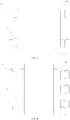
FIGS. 3-6 are schematic top views of several kinds of inductance devices of the present application which are provided respectively with different number of auxiliary winding parts; -
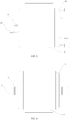
FIG. 7 is a schematic view of a welding structure of the inductance device of the present application and a PCB; -
FIG. 8 is a schematic perspective view of an inductance device of the present application with the same auxiliary coil simultaneously wound around a plurality of auxiliary winding parts; -
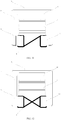
FIGS. 9-12 are schematic views of several kinds of inductance devices of the present application which are provided with auxiliary coils wound in different winding ways, respectively; -
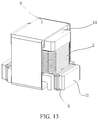
FIG. 13 is a schematic perspective view of an inductance device of the present application which is provided with elongated auxiliary winding parts. - 1- inductor framework, 10- main winding part, 100- upper end, 100a- top surface, 100b- first groove, 102- lower end, 102a- bottom surface, 102b- lower through groove, 102c- wire routing groove, 102d- surface of lower end facing upper end, 104- main body, 104a- main winding groove, 106- inserting hole, 12- auxiliary winding part, 120-welding surface, 121,122- vertical surface, 123- surface, 124- surface of the auxiliary winding part facing away from lower end, 125- position limiting structure/position limiting groove, 2- main coil, 3- upper magnetic core, 30- central column, 32- surface of upper magnetic core facing away from lower magnetic core, 4- lower magnetic core, 40- central column, 5- auxiliary coil, 6- attaching structure, 7- PCB.
- The technical solutions of the present application will be clearly and completely described below in connection with particular embodiments of the present application and corresponding accompanying drawings, so that the objectives, technical solutions and advantages of the present application are more understandable. Apparently, the described embodiments are just a part but not all of the embodiments of the present application. Based on the described embodiments of the present application, those skilled in the art can obtain other embodiment(s), without any inventive work, which should be within the scope of the present application.
- In the following, technical solutions provided by embodiments of the present application will be described in detail in connection with the drawings.
- An embodiment of the present application discloses an inductance device, as shown in
FIG. 1 , including aninductor framework 1, amain coil 2, an uppermagnetic core 3, a lowermagnetic core 4, andauxiliary coils 5. - The inductor framework in the embodiment can be made from insulating materials, and it is recommended to use phenolic plastics as the materials of the inductor framework for reduction of cost. Specifically, as shown in
FIGS. 2-6 , theinductor framework 1 includes a main windingpart 10 andauxiliary winding parts 12 that are integrally arranged. The main windingpart 10 includes anupper end 100, alower end 102, amain body 104 located between theupper end 100 and thelower end 102, and aninserting hole 106. Edges of both theupper end 100 and thelower end 102 go beyond themain body 104, and cooperate with themain body 104 to form a mainwinding groove 104a in which themain coil 2 is wound. Theupper end 100 and thelower end 102 can restrict the form of themain coil 2 to prevent themain coil 2 from separating from themain body 104. Theupper end 100 has atop surface 100a facing away from the lower end, and thelower end 102 also has abottom surface 102a facing away from theupper end 100. Theinserting hole 106 passes successively through theupper end 100, themain body 104, and thelower end 102 in the direction from thetop surface 100a to thebottom surface 102a. - The
auxiliary winding parts 12 extend towards the direction away from the insertinghole 106 from thelower end 102. Theauxiliary winding parts 12 have extension directions perpendicular to that of the insertinghole 106, and namely theauxiliary winding parts 12 are arranged at sides of the insertinghole 106. Side surfaces of the auxiliary windingparts 102b facing away from theupper end 100 are weldingsurfaces 120 which are at a distance from thetop surface 100a in the extension direction of the insertinghole 106 no less than a distance between thebottom surface 102a and thetop surface 100a in the extension direction of the insertinghole 106, and in other words the welding surfaces 120 are at a lower location than thebottom surface 102a so as to be welded with a PCB. Theauxiliary winding parts 12 are used to wind theauxiliary coils 5 around them, and theauxiliary coils 5 wound thereon can cover at least a portion of the welding surfaces 120 to be used for welding. There is no special limit to the shape of theauxiliary coils 5, as long as theauxiliary coil 5 can cover a portion of thewelding surface 120. For example, it is possible to wind theauxiliary coil 5 annularly between two vertical surfaces 121,122 adjacent to thewelding surface 120 and asurface 123 of the auxiliary windingpart 12 facing theupper end 100, or between the two vertical surfaces 121,122 and asurface 124 of the auxiliary windingpart 12 facing away from thelower end 102, and it is also possible to wind theauxiliary coils 5 in other more complicated way, which will not be discussed herein. - In order to prevent the
auxiliary coil 5 from separating from theauxiliary winding part 12, it is necessary to arrange on the auxiliary winding parts 12 aposition limiting structure 125 which restricts theauxiliary coil 5 to prevent theauxiliary coil 5 from separating from theauxiliary winding part 12. In the embodiment, theposition limiting structure 125 may be arranged on an arbitrary surface of the auxiliary windingpart 12. Theauxiliary coils 5 are of an integral structure, so the objection of preventing theauxiliary coils 5 from separating from the auxiliaryposition limiting parts 12 can be achieved as long as any portion of theauxiliary coils 5 is prevented from separating from theauxiliary winding parts 12. However, in order to ensure the welding effect, thewelding surface 120 is preferably as close as possible to the PCB when assembling the inductance device. Thus, it is preferred for theposition limiting structures 125 in the embodiment to be arranged on other surfaces of the auxiliary windingparts 12 rather than the welding surfaces 120. - In the embodiment, the
position limiting structure 125 may be the structure such as a position limiting block, a position limiting baffle plate, etc., and it is recommended to use the form of a position limiting groove. The position limiting groove 125 (for the sake of description, thereference number 125 of the position limiting structure is used for the position limiting groove in the following) can receive a portion of theauxiliary coil 5 so that the portion of theauxiliary coil 5 cannot separate from theauxiliary winding part 12. Theposition limiting groove 125 extends in a direction identical, perpendicular, or even inclined to the extension direction of the insertinghole 106. The number of theposition limiting groove 125 can be more than one. For example, thevertical surfaces position limiting groove 125, respectively; or thevertical surface 121 is provided with oneposition limiting groove 125 which has the same extension direction as the insertinghole 106, and thesurface 124 is provided with oneposition limiting groove 125 which extends in a direction perpendicular to the extension direction of the inserting hole 106 (seeFIG. 2 ), and the plurality ofposition limiting grooves 125 cooperate with each other to limit the position of theauxiliary coil 5. Furthermore, it is also possible to arrange multiple segments ofposition limiting grooves 125, examples of which will not be given herein. - In the embodiment, the
main coil 2 and theauxiliary coils 5 can be wound successively with the same enameled wire when winding, and there is electrical connection between themain coil 2 and theauxiliary coils 5 that are wound, so that theauxiliary coils 5 can supply power directly for themain coil 2. Furthermore, themain coil 2 and theauxiliary coils 5 in the embodiment can also be wound with different enameled wires, respectively, and in this case there is no electrical connection between theauxiliary coil 5 and themain coil 2, theauxiliary coils 5 are only used for fixing and welding. - It is necessary for the
main coil 2 to have at least one input end and one output end, and thus, in the usual case at least two of theauxiliary coils 5 are wound with the same enameled wire as themain coil 2. The twoauxiliary coils 5 can be used as the input end and the output end of themain coil 2, respectively. Of course, to cope with different application environments, the number of the input end and the output end of themain coil 2 can be changed, and the number of theauxiliary coils 5 in electrical connection with themain coil 2 can be increased further. - As shown in
FIG. 1 , both the uppermagnetic core 3 and the lowermagnetic core 4 in the embodiment are E-shaped structures, middle extension portions of the E-shaped structures arecentral column main coil 2 and theauxiliary coils 5 is finished, the uppermagnetic core 3 is capped onto thetop surface 100a, and thecentral column 30 of the uppermagnetic core 3 is inserted into the insertinghole 106 from an opening of the insertinghole 6 at theupper end 100, and extension portions at two sides of the uppermagnetic core 3 cover the outer periphery of themain coil 2. The lowermagnetic core 4 is capped onto thebottom surface 102a, and thecentral column 40 of the lowermagnetic core 4 is inserted into the insertinghole 106 from an opening of the insertinghole 6 at thelower end 102. It is required that the side surface of the lowermagnetic core 4 facing away from the uppermagnetic core 3 should not go beyond thewelding surface 102 in order to avoid affecting the welding effect. In order to prevent the side surface of the lowermagnetic core 4 facing away from the uppermagnetic core 3 from going beyond the welding surface, it is possible in design to form a height difference between thewelding surface 120 and thebottom surface 102a enough to receive the lowermagnetic core 4, or to arrange a lower throughgroove 102b in thebottom surface 102a which is used to receive the lowermagnetic core 4. In this case, in order to insert thecentral column 40 into the insertinghole 106, it is necessary for the insertinghole 106 to extend to the lower throughgroove 102b. At the same time, in order to prevent the lowermagnetic core 4 from interfering with the auxiliary windingparts 12, theauxiliary winding parts 12 extend in directions perpendicular to the extension direction of the lower throughgroove 102b, and namely theauxiliary winding parts 12 are arranged at sides of the lower throughgroove 102b. - When the inductance device is assembled onto the
PCB 7, a portion of the enamel of theauxiliary coils 5 covering the welding surfaces 120 is melt by high temperature to expose internal metal wires. Under high temperature the metal wires will melt and flow onto a bonding pad on thePCB 7, and after cooling and solidifying, the welding operation of theauxiliary coils 5 and the bonding pad can be finished (seeFIG. 7 ). Because it is unnecessary to reserve the region in the bonding pad for the pins to pass through, the boding pad has an area reduced greatly and even can completely be hidden under the inductance device, thus greatly saving the area of thePCB 7. - To improve the stability of assembly, it is possible that the
auxiliary winding parts 12 extend at two sides of thelower end 102 symmetric to the insertinghole 106 and theauxiliary coils 5 are wound around auxiliary windingparts 12 at each side, so that the inductance device can have a welded connection with the PCB at its two sides by theauxiliary coils 5 during the welding operation, and the high stability is obtained. The number of the auxiliary windingparts 12 and theauxiliary coils 5 can be adjusted according to the required structural strength and the need for electrical connection. Usually, the number of the auxiliary windingparts 12 is in a range from two to five, and it is preferred to use the technical solution with four auxiliary winding parts, and any two of the four auxiliary winding parts are symmetrical to each other. - In the embodiment, usually each
auxiliary coil 5 is separately wound around oneauxiliary winding part 12, and however oneauxiliary coil 5 being simultaneously wound around a plurality of the auxiliary windingparts 12 at the same side of thelower end 102 is not excluded in the embodiment. For example, in the technical solution shown inFIG. 8 , the two auxiliary windingparts 12 at the same side can be used as two supporting points around which the enameled wire is wound to form an elongatedauxiliary coil 5. This kind ofauxiliary coil 5 and the PCB have a larger welding area, and the better structural stability and electrical stability are obtained. Of course, when winding, in addition to the two auxiliary windingparts 12 as the supporting points, other auxiliary winding parts 15 can be included in the middle of theauxiliary coil 5 to support the middle part, and therefore the sameauxiliary coil 5 can be simultaneously wound around two or more auxiliary windingparts 12. - In addition, as shown in
FIGS. 9 to 12 , the enameled wire can be led from asurface 123 of oneauxiliary winding part 12 to asurface 123 of the otherauxiliary winding part 123, or from awelding surface 120 of oneauxiliary winding part 12 to awelding surface 120 of the otherauxiliary winding part 12; and the enameled wire can also be led from asurface 123/welding surface 120 of oneauxiliary winding part 12 to asurface 123/welding surface 120 of the otherauxiliary winding part 12, thus forming a slash or crossing structure. In addition to the structures described above, as shown inFIG. 13 , in some embodiments, it is also possible that the enameled wire is wound around theauxiliary winding part 5 which is lengthened to form an elongatedauxiliary coil 5. - When the enameled wire is required to extend to the
auxiliary winding part 12 after being wound to form themain coil 2, or when the enameled wire is required to extend to the main windinggroove 104a after being wound to form theauxiliary coil 5, it is necessary for the enameled wire to extend for a distance to arrive at the auxiliary windingparts 12 or the main windinggroove 104a. For the regularization of the enameled wire within the distance to make the whole of coils tidier, as shown inFIG. 2 , in the embodiment, thelower end 102 are also provided withwire routing grooves 102c which are located at one side of thelower end 102 facing theupper end 100 and extend from the main windinggroove 104a to sides of the auxiliary winding parts facing theupper end 100, namely the sides where thesurfaces 123 are located, so that the enameled wire can transfer between the main windinggroove 104a and theauxiliary winding parts 12 through thewire routing grooves 102c. The portion of the enameled wire between themain coil 2 and theauxiliary coils 5 will be restricted by thewire routing grooves 102c, thus forming a tidy appearance. - In order to prevent the
wire routing grooves 102c from affecting the winding of themain coil 2, thewire routing grooves 102c cannot protrude from thesurface 102d of thelower end 102 facing theupper end 100. Therefore, in the present embodiment, the side of the auxiliary windingparts 12 facing theupper end 100 are at a distance from theupper end 100 in the extension direction of the insertinghole 106 greater than the distance between thesurface 102d of thelower end 102 facing theupper end 100 and theupper end 100 in the extension direction of the insertinghole 106, and namely the sides of the auxiliary windingparts 12 facing theupper end 100 are at a farther distance from theupper end 100. In this way, thewire routing grooves 102c can form inclined grooves to gradually move away from theupper end 100 in an oblique way from thesurface 102d and finally extend to theauxiliary winding parts 12, thus avoiding thewire routing grooves 102c from protruding from thesurface 102d. - The sides of the auxiliary winding
parts 12 facing theupper end 100 can be thesurfaces 123, and can be the bottoms of theposition limiting grooves 125 in the case whereposition limiting grooves 125 are provided at thesurfaces 123. - For mechanized production, an attaching mechanism is usually used when transferring the inductance device, and for the convenience of attaching, it is necessary to arrange an attaching surface easy to be attached in the inductance device. With respect to the inductance device, the
surface 32 of the uppermagnetic core 3 facing away from the lowermagnetic core 4 is an integral surface of a large area, and therefore is usually used as an attaching surface. With miniaturization of the inductance device, thesurface 32 has a decreased area to make it more difficult to meet attaching requirements. - For the improvement of the attaching effect of the miniaturized inductance device, as shown in
FIG. 2 , in the present embodiment, thetop surface 100a is also provided with an upper throughgroove 100b to which the insertinghole 106 extends. It should be noted that the upper throughgroove 100b extends in a direction perpendicular to the extension directions of the auxiliary windingparts 12, because it is necessary for the lowermagnetic core 4 to avoid theauxiliary winding parts 12 and to be arranged oppositely to the uppermagnetic core 3. Meanwhile, it is also necessary for an attachingstructure 6 to be arranged in the inductance device. When assembling the uppermagnetic core 3 with theinductor framework 1, the uppermagnetic core 3 is capped into the upper throughgroove 100b, so that thesurface 32 is flush with thetop surface 100a, and the attachingstructure 6 simultaneously covers thesurface 32 and at least a portion of thetop surface 100a (seeFIG. 8 ). In this case, the attaching area includes a portion of thetop surface 100a in addition to thesurface 32, thereby increasing the attaching area and improving the attaching effect. - In the embodiment, the attaching
structure 6 can be a baffle plate which is attached onto thesurface 32 and at least a portion of thetop surface 100a. Because the inductance device generates lots of heat in working condition, it is possible to use the baffle plate made from a high temperature resistant insulation material to avoid the damage of the baffle plate. - In addition, a high temperature resistant adhesive tape is also used for the attaching
structure 6. The adhesive tape is wound in the extension direction of the upper throughgroove 100b to cover outer circumferences of the uppermagnetic core 3 and the lowermagnetic core 4 and at least a portion of thetop surface 100a. The upper throughgroove 100b and the lower throughgroove 102b in the embodiment can be arranged simultaneously, or one of them can be arranged separately. If there are both the upper throughgroove 100b and the lower throughgroove 102b, the upper throughgroove 100b has the same extension direction as the lower throughgroove 102b. In this case, it is necessary for the adhesive tape to cover a portion of thetop surface 100a, the adhesive tape has a width larger than that of the uppermagnetic core 3 and larger than that of the lowermagnetic core 4. If the lower throughgroove 102b has the same notch size as the upper throughgroove 100b, the adhesive tape not only goes beyond the upper throughgroove 100b to cover thetop surface 100a during winding, but also goes beyond the lower throughgroove 102b. However, the adhesive tape going beyond the lower throughgroove 102b can affect adversely the welding process, so it is recommended in the embodiment that the lower throughgroove 102b of theinductor framework 1 is designed to have a notch size larger than that of the upper throughgroove 102a, so as to receive the adhesive tape. - The inductor framework and the inductance device provided by the embodiments of the present application can greatly save the area of the PCB.
- The above embodiments of this application focus on the differences between the various embodiments. As long as the different optimization features between the various embodiments are not contradictory, they can be combined to form a better embodiment, without repeated here considering the conciseness of the text.
- The above descriptions are only embodiments of this application and are not used to be construed as any limitation to the present application. For those skilled in the art, the present application can have various modifications and changes. Any modification, equivalent replacement, improvement, etc. made within the spirit and principle of the present application shall be included in the scope of the claims of the present application.
Claims (20)
- An inductor framework, characterized in that the inductor framework comprises a main winding part and an auxiliary winding part that are integrally arranged;
wherein the main winding part comprises an upper end, a lower end, a main body, and an inserting hole; the main body is located between the upper end and the lower end, edges of both the upper end and the lower end go beyond the main body and cooperate with the main body to form a main winding groove; the upper end has a top surface facing away from the lower end, and the lower end has a bottom surface facing away from the upper end; the inserting hole successively passes through the upper end, the main body, and the lower end in a direction from the top surface to the bottom surface; and
wherein the auxiliary winding part extends towards a direction away from the inserting hole from the lower end, and the auxiliary winding part has an extension direction perpendicular to that of the inserting hole; a side surface of the auxiliary winding part facing away from the upper end is a welding surface which is at a distance from the top surface in the extension direction of the inserting hole no less than a distance between the bottom surface and the top surface in the extension direction of the inserting hole; the auxiliary winding part is configured to be wound thereon an auxiliary coil which at least covers a portion of the welding surface, the auxiliary winding part is provided with a position limiting structure configured to prevent the auxiliary coil that is wound around the auxiliary winding part from separating from the auxiliary winding part. - The inductor framework according to claim 1, characterized in that the position limiting structure is a position limiting groove configured to receive a portion of the auxiliary coil.
- The inductor framework according to claim 2, characterized in that the position limiting groove extends in a direction identical and/or perpendicular to the extension direction of the inserting hole.
- The inductor framework according to any one of claims 1-3, characterized in that the auxiliary position limiting part extends at two sides of the lower end symmetrical to the inserting hole.
- The inductor framework according to claim 4, characterized in that the number of the auxiliary parts is in a range from two to five.
- The inductor framework according to claim 5, characterized in that four auxiliary winding parts are provided, and any two of the four auxiliary winding parts are symmetrical to each other.
- The inductor framework according to any one of claims 1-3, characterized in that the top surface is provided with an upper through groove to which the inserting hole extends, and the auxiliary winding part extends in a direction perpendicular to an extension direction of the upper through groove.
- The inductor framework according to any one of claims 1-3, characterized in that the bottom surface is provided with a lower through groove to which the inserting hole extends, and the auxiliary winding part extends in a direction perpendicular to an extension direction of the lower through groove.
- The inductor framework according to claim 8, characterized in that the top surface is provided with an upper through groove to which the inserting hole extends, an extension direction of the upper through groove is the same as that of the lower through groove, and a notch size of the lower through groove is a larger than that of the upper through groove.
- The inductor framework according to any one of claims 1-3, characterized in that the lower end is further provided with a wire routing groove, and the wire routing groove is located at a side of the lower end facing the upper end and extends to a side of the auxiliary winding part facing the upper end from the main winding groove.
- The inductor framework according to claim 10, characterized in that a distance between the side of the auxiliary winding part facing the upper end and the upper end in the extension direction of the inserting hole is greater than a distance between the side of the lower end facing the upper end and the upper end in the extension direction of the inserting hole, and the wire routing groove is an inclined groove.
- The inductor framework according to any one of claims 1-3, characterized in that the inductor framework is an inductor framework of phenolic plastic.
- An inductance device, characterized in that the inductance device comprises a main coil, an auxiliary coil, an upper magnetic core, a lower magnetic core, and the inductor framework according to any one of claims 1-12; and
wherein the main coil is wound in the main winding groove, the auxiliary coil is wound around the auxiliary winding part and covers a portion of the welding surface; both the upper magnetic core and the lower magnetic core are E-shaped structures, a middle extension portion of each of the E-shaped structures is a central column; the upper magnetic core is capped onto the top surface, the central column of the upper magnetic core is inserted into the inserting hole, the lower magnetic core is capped onto the bottom surface, the central column of the lower magnetic core is also inserted into the inserting hole, and a side surface of the lower magnetic core facing away from the upper magnetic core does not go beyond the welding surface. - The inductance device according to claim 13, characterized in that the main coil and the auxiliary coil are formed by winding with the same enameled wire or different enameled wires.
- The inductance device according to claim 14, characterized in that the auxiliary coil comprises at least two auxiliary coils, and the main coil and at least two of the auxiliary coils are formed by winding with the same enameled wire.
- The inductance device according to claim 13, characterized in that the auxiliary coil comprises at least one auxiliary coil which is wound separately around one of the auxiliary winding part.
- The inductance device according to claim 13, characterized in that the auxiliary coil comprises at least one auxiliary coil, at least one auxiliary coil is wound simultaneously around a plurality of auxiliary winding parts at the same side of the lower end.
- The inductance device according to any one of claims 13-17, characterized in that the top surface is provided with an upper through groove to which the inserting hole extends, and the auxiliary winding part extends in a direction perpendicular to an extension direction of the upper through groove; and
wherein the inductance device further comprises an attaching structure; the upper magnetic core is capped onto the upper through groove, a surface of the upper magnetic core facing away from the lower magnetic core is flush with the top surface, and the attaching structure covers both the surface of the upper magnetic core facing away from the lower magnetic core and at least a portion of the top surface. - The inductance device according to claim 18, characterized in that the bottom surface is provided with a lower through groove which extends in the same direction as the upper through groove, the inserting hole extends to the lower through groove, and a notch size of the lower through groove is larger than that of the upper through groove; and
wherein the attaching structure is an adhesive tape which is wound in the extension direction of the lower through groove to cover an outer circumference of both the upper magnetic core and the lower magnetic core and to cover at least a portion of the top surface. - The inductance device according to claim 18, characterized in that the attaching structure is a baffle plate which is attached onto both a surface of the upper magnetic core facing away from the lower magnetic core and at least a portion of the top surface.
Applications Claiming Priority (3)
| Application Number | Priority Date | Filing Date | Title |
|---|---|---|---|
| CN201821169172.1U CN208767130U (en) | 2018-07-23 | 2018-07-23 | Inductance framework and inductance device |
| CN201810813649.3A CN108831715A (en) | 2018-07-23 | 2018-07-23 | inductance framework and inductance device |
| PCT/CN2019/097135 WO2020020106A1 (en) | 2018-07-23 | 2019-07-22 | Inductor core and inductor device |
Publications (3)
| Publication Number | Publication Date |
|---|---|
| EP3800652A1 true EP3800652A1 (en) | 2021-04-07 |
| EP3800652A4 EP3800652A4 (en) | 2021-09-15 |
| EP3800652B1 EP3800652B1 (en) | 2026-04-08 |
Family
ID=69181086
Family Applications (1)
| Application Number | Title | Priority Date | Filing Date |
|---|---|---|---|
| EP19840590.4A Active EP3800652B1 (en) | 2018-07-23 | 2019-07-22 | Inductance device |
Country Status (3)
| Country | Link |
|---|---|
| US (1) | US11862368B2 (en) |
| EP (1) | EP3800652B1 (en) |
| WO (1) | WO2020020106A1 (en) |
Cited By (1)
| Publication number | Priority date | Publication date | Assignee | Title |
|---|---|---|---|---|
| CN114334354A (en) * | 2021-12-16 | 2022-04-12 | 湖南省冠群电子科技有限公司 | Integrated into one piece inductance of high shock resistance anti-vibration |
Families Citing this family (1)
| Publication number | Priority date | Publication date | Assignee | Title |
|---|---|---|---|---|
| CN117524661A (en) * | 2023-12-14 | 2024-02-06 | 深圳顺络汽车电子有限公司 | Magnetic devices |
Family Cites Families (16)
| Publication number | Priority date | Publication date | Assignee | Title |
|---|---|---|---|---|
| JPH0726819Y2 (en) * | 1987-12-07 | 1995-06-14 | 株式会社トーキン | Coil / transformer for surface mounting |
| JPH0548314U (en) * | 1991-11-28 | 1993-06-25 | 株式会社トーキン | Extra-fine wire cord terminal |
| JPH06260342A (en) * | 1993-03-09 | 1994-09-16 | Taiyo Yuden Co Ltd | Surface-mount type coil component |
| JP3337108B2 (en) * | 1995-11-07 | 2002-10-21 | オリジン電気株式会社 | Common mode choke coil |
| US8698587B2 (en) * | 2010-07-02 | 2014-04-15 | Samsung Electro-Mechanics Co., Ltd. | Transformer |
| CN202394675U (en) * | 2011-12-30 | 2012-08-22 | 江苏利通电子有限公司 | Ultrathin transformer with lead wire guide slot |
| KR101388797B1 (en) * | 2012-06-29 | 2014-04-23 | 삼성전기주식회사 | Coil component, mounting structure thereof, and electronic device having the same |
| CN104488043A (en) * | 2012-08-01 | 2015-04-01 | 株式会社村田制作所 | Transformer coil |
| CN203338939U (en) * | 2013-06-26 | 2013-12-11 | 深圳市精日昌电子科技有限公司 | Widened framework used for transformer |
| KR20150050025A (en) * | 2013-10-31 | 2015-05-08 | 삼성전기주식회사 | Coil component |
| CN206179657U (en) * | 2016-11-15 | 2017-05-17 | 东莞铭普光磁股份有限公司 | High paster transformer of keeping apart of double -deck pin |
| JP6895246B2 (en) * | 2016-12-26 | 2021-06-30 | Njコンポーネント株式会社 | Trance and bobbin |
| CN108831715A (en) * | 2018-07-23 | 2018-11-16 | 苏州欧普照明有限公司 | inductance framework and inductance device |
| CN208767130U (en) * | 2018-07-23 | 2019-04-19 | 苏州欧普照明有限公司 | Inductance framework and inductance device |
| EP3975208A4 (en) * | 2019-09-09 | 2023-07-19 | Suzhou Opple Lighting Co., Ltd. | Inductance frame, inductance apparatus and light fixture |
| EP3975209B1 (en) * | 2019-09-09 | 2025-04-30 | Suzhou Opple Lighting Co., Ltd. | Inductor framework structure, inductor device and lamp |
-
2019
- 2019-07-22 WO PCT/CN2019/097135 patent/WO2020020106A1/en not_active Ceased
- 2019-07-22 EP EP19840590.4A patent/EP3800652B1/en active Active
-
2020
- 2020-12-31 US US17/139,799 patent/US11862368B2/en active Active
Cited By (1)
| Publication number | Priority date | Publication date | Assignee | Title |
|---|---|---|---|---|
| CN114334354A (en) * | 2021-12-16 | 2022-04-12 | 湖南省冠群电子科技有限公司 | Integrated into one piece inductance of high shock resistance anti-vibration |
Also Published As
| Publication number | Publication date |
|---|---|
| EP3800652B1 (en) | 2026-04-08 |
| EP3800652A4 (en) | 2021-09-15 |
| US20210125771A1 (en) | 2021-04-29 |
| WO2020020106A1 (en) | 2020-01-30 |
| US11862368B2 (en) | 2024-01-02 |
Similar Documents
| Publication | Publication Date | Title |
|---|---|---|
| JP6930177B2 (en) | Transformers and transformer manufacturing methods | |
| CN103035364B (en) | Electronic transformer | |
| US20120319812A1 (en) | Assembling magnetic component | |
| CN110517863A (en) | Inductance framework and inductance device | |
| US12451285B2 (en) | Inductor skeleton structure, inductance device and luminaire | |
| CN214476891U (en) | Inductors and electrical components containing the same | |
| CN109378180B (en) | On-board integrated transformer | |
| EP3800652B1 (en) | Inductance device | |
| JP2013115378A (en) | Transformer | |
| EP3975208A1 (en) | Inductance frame, inductance apparatus and light fixture | |
| EP3979274B1 (en) | Inductive framework, inductive device, and lamp | |
| CN211427963U (en) | Common-differential-mode integrated inductor convenient for automatic processing | |
| CN103915246A (en) | Coil component | |
| CN212062136U (en) | Multipurpose integrated transformer | |
| CN203721458U (en) | High-frequency transformer | |
| CN103065770A (en) | Induction device | |
| CN110739131A (en) | Magnetic core, transformer and power supply | |
| CN210272031U (en) | Inductive bobbins, inductive devices and lamps | |
| KR20170103267A (en) | Inductor And Method Of Fabricating The Same | |
| JP3174593U (en) | Building block combination high power transformer | |
| TWM519803U (en) | Integrated core structure and integrated magnetic components | |
| JP2010251364A (en) | Bobbin for coil, winding component, coil component, switching power supply unit, and method of manufacturing coil component | |
| CN205194479U (en) | Power transformer and have this power transformer's gas shielded arc welding equipment | |
| CN222952896U (en) | A transformer structure for reducing temperature rise | |
| CN201017759Y (en) | Transformer structure |
Legal Events
| Date | Code | Title | Description |
|---|---|---|---|
| STAA | Information on the status of an ep patent application or granted ep patent |
Free format text: STATUS: THE INTERNATIONAL PUBLICATION HAS BEEN MADE |
|
| PUAI | Public reference made under article 153(3) epc to a published international application that has entered the european phase |
Free format text: ORIGINAL CODE: 0009012 |
|
| STAA | Information on the status of an ep patent application or granted ep patent |
Free format text: STATUS: REQUEST FOR EXAMINATION WAS MADE |
|
| 17P | Request for examination filed |
Effective date: 20201228 |
|
| AK | Designated contracting states |
Kind code of ref document: A1 Designated state(s): AL AT BE BG CH CY CZ DE DK EE ES FI FR GB GR HR HU IE IS IT LI LT LU LV MC MK MT NL NO PL PT RO RS SE SI SK SM TR |
|
| AX | Request for extension of the european patent |
Extension state: BA ME |
|
| REG | Reference to a national code |
Ref country code: DE Ref legal event code: R079 Free format text: PREVIOUS MAIN CLASS: H01F0027280000 Ipc: H01F0027320000 |
|
| A4 | Supplementary search report drawn up and despatched |
Effective date: 20210817 |
|
| RIC1 | Information provided on ipc code assigned before grant |
Ipc: H01F 27/28 20060101ALI20210811BHEP Ipc: H01F 27/29 20060101ALI20210811BHEP Ipc: H01F 27/32 20060101AFI20210811BHEP |
|
| DAV | Request for validation of the european patent (deleted) | ||
| DAX | Request for extension of the european patent (deleted) | ||
| STAA | Information on the status of an ep patent application or granted ep patent |
Free format text: STATUS: EXAMINATION IS IN PROGRESS |
|
| 17Q | First examination report despatched |
Effective date: 20231201 |
|
| RIC1 | Information provided on ipc code assigned before grant |
Ipc: H01F 27/32 20060101AFI20251008BHEP Ipc: H01F 27/28 20060101ALI20251008BHEP Ipc: H01F 27/29 20060101ALI20251008BHEP Ipc: H01F 17/04 20060101ALI20251008BHEP Ipc: H01F 27/30 20060101ALI20251008BHEP Ipc: H01F 5/04 20060101ALI20251008BHEP Ipc: H01F 27/06 20060101ALI20251008BHEP |
|
| GRAP | Despatch of communication of intention to grant a patent |
Free format text: ORIGINAL CODE: EPIDOSNIGR1 |
|
| STAA | Information on the status of an ep patent application or granted ep patent |
Free format text: STATUS: GRANT OF PATENT IS INTENDED |
|
| INTG | Intention to grant announced |
Effective date: 20251114 |
|
| GRAS | Grant fee paid |
Free format text: ORIGINAL CODE: EPIDOSNIGR3 |
|
| GRAA | (expected) grant |
Free format text: ORIGINAL CODE: 0009210 |
|
| STAA | Information on the status of an ep patent application or granted ep patent |
Free format text: STATUS: THE PATENT HAS BEEN GRANTED |
|
| AK | Designated contracting states |
Kind code of ref document: B1 Designated state(s): AL AT BE BG CH CY CZ DE DK EE ES FI FR GB GR HR HU IE IS IT LI LT LU LV MC MK MT NL NO PL PT RO RS SE SI SK SM TR |
|
| REG | Reference to a national code |
Ref country code: CH Ref legal event code: F10 Free format text: ST27 STATUS EVENT CODE: U-0-0-F10-F00 (AS PROVIDED BY THE NATIONAL OFFICE) Effective date: 20260408 Ref country code: GB Ref legal event code: FG4D |
|
| REG | Reference to a national code |
Ref country code: DE Ref legal event code: R096 Ref document number: 602019083469 Country of ref document: DE |