EP3799286A1 - Control system and power supply unit - Google Patents
Control system and power supply unit Download PDFInfo
- Publication number
- EP3799286A1 EP3799286A1 EP19807575.6A EP19807575A EP3799286A1 EP 3799286 A1 EP3799286 A1 EP 3799286A1 EP 19807575 A EP19807575 A EP 19807575A EP 3799286 A1 EP3799286 A1 EP 3799286A1
- Authority
- EP
- European Patent Office
- Prior art keywords
- time
- voltage
- threshold voltage
- unit
- power supply
- Prior art date
- Legal status (The legal status is an assumption and is not a legal conclusion. Google has not performed a legal analysis and makes no representation as to the accuracy of the status listed.)
- Granted
Links
Images



Classifications
-
- H—ELECTRICITY
- H03—ELECTRONIC CIRCUITRY
- H03K—PULSE TECHNIQUE
- H03K5/00—Manipulating of pulses not covered by one of the other main groups of this subclass
- H03K5/22—Circuits having more than one input and one output for comparing pulses or pulse trains with each other according to input signal characteristics, e.g. slope, integral
- H03K5/24—Circuits having more than one input and one output for comparing pulses or pulse trains with each other according to input signal characteristics, e.g. slope, integral the characteristic being amplitude
-
- H—ELECTRICITY
- H02—GENERATION; CONVERSION OR DISTRIBUTION OF ELECTRIC POWER
- H02M—APPARATUS FOR CONVERSION BETWEEN AC AND AC, BETWEEN AC AND DC, OR BETWEEN DC AND DC, AND FOR USE WITH MAINS OR SIMILAR POWER SUPPLY SYSTEMS; CONVERSION OF DC OR AC INPUT POWER INTO SURGE OUTPUT POWER; CONTROL OR REGULATION THEREOF
- H02M3/00—Conversion of DC power input into DC power output
- H02M3/22—Conversion of DC power input into DC power output with intermediate conversion into AC
- H02M3/24—Conversion of DC power input into DC power output with intermediate conversion into AC by static converters
- H02M3/28—Conversion of DC power input into DC power output with intermediate conversion into AC by static converters using discharge tubes with control electrode or semiconductor devices with control electrode to produce the intermediate AC
- H02M3/325—Conversion of DC power input into DC power output with intermediate conversion into AC by static converters using discharge tubes with control electrode or semiconductor devices with control electrode to produce the intermediate AC using devices of a triode or a transistor type requiring continuous application of a control signal
- H02M3/335—Conversion of DC power input into DC power output with intermediate conversion into AC by static converters using discharge tubes with control electrode or semiconductor devices with control electrode to produce the intermediate AC using devices of a triode or a transistor type requiring continuous application of a control signal using semiconductor devices only
-
- G—PHYSICS
- G05—CONTROLLING; REGULATING
- G05B—CONTROL OR REGULATING SYSTEMS IN GENERAL; FUNCTIONAL ELEMENTS OF SUCH SYSTEMS; MONITORING OR TESTING ARRANGEMENTS FOR SUCH SYSTEMS OR ELEMENTS
- G05B19/00—Program-control systems
- G05B19/02—Program-control systems electric
- G05B19/04—Program control other than numerical control, i.e. in sequence controllers or logic controllers
- G05B19/05—Programmable logic controllers, e.g. simulating logic interconnections of signals according to ladder diagrams or function charts
- G05B19/058—Safety, monitoring
-
- G—PHYSICS
- G06—COMPUTING OR CALCULATING; COUNTING
- G06F—ELECTRIC DIGITAL DATA PROCESSING
- G06F1/00—Details not covered by groups G06F3/00 - G06F13/00 and G06F21/00
- G06F1/26—Power supply means, e.g. regulation thereof
- G06F1/28—Supervision thereof, e.g. detecting power-supply failure by out of limits supervision
-
- G—PHYSICS
- G06—COMPUTING OR CALCULATING; COUNTING
- G06F—ELECTRIC DIGITAL DATA PROCESSING
- G06F1/00—Details not covered by groups G06F3/00 - G06F13/00 and G06F21/00
- G06F1/26—Power supply means, e.g. regulation thereof
- G06F1/30—Means for acting in the event of power-supply failure or interruption, e.g. power-supply fluctuations
-
- G—PHYSICS
- G06—COMPUTING OR CALCULATING; COUNTING
- G06F—ELECTRIC DIGITAL DATA PROCESSING
- G06F1/00—Details not covered by groups G06F3/00 - G06F13/00 and G06F21/00
- G06F1/26—Power supply means, e.g. regulation thereof
- G06F1/30—Means for acting in the event of power-supply failure or interruption, e.g. power-supply fluctuations
- G06F1/305—Means for acting in the event of power-supply failure or interruption, e.g. power-supply fluctuations in the event of power-supply fluctuations
-
- H—ELECTRICITY
- H02—GENERATION; CONVERSION OR DISTRIBUTION OF ELECTRIC POWER
- H02M—APPARATUS FOR CONVERSION BETWEEN AC AND AC, BETWEEN AC AND DC, OR BETWEEN DC AND DC, AND FOR USE WITH MAINS OR SIMILAR POWER SUPPLY SYSTEMS; CONVERSION OF DC OR AC INPUT POWER INTO SURGE OUTPUT POWER; CONTROL OR REGULATION THEREOF
- H02M1/00—Details of apparatus for conversion
- H02M1/36—Means for starting or stopping converters
-
- G—PHYSICS
- G05—CONTROLLING; REGULATING
- G05B—CONTROL OR REGULATING SYSTEMS IN GENERAL; FUNCTIONAL ELEMENTS OF SUCH SYSTEMS; MONITORING OR TESTING ARRANGEMENTS FOR SUCH SYSTEMS OR ELEMENTS
- G05B2219/00—Program-control systems
- G05B2219/10—Plc systems
- G05B2219/15—Plc structure of the system
- G05B2219/15097—Power supply
-
- H—ELECTRICITY
- H02—GENERATION; CONVERSION OR DISTRIBUTION OF ELECTRIC POWER
- H02M—APPARATUS FOR CONVERSION BETWEEN AC AND AC, BETWEEN AC AND DC, OR BETWEEN DC AND DC, AND FOR USE WITH MAINS OR SIMILAR POWER SUPPLY SYSTEMS; CONVERSION OF DC OR AC INPUT POWER INTO SURGE OUTPUT POWER; CONTROL OR REGULATION THEREOF
- H02M1/00—Details of apparatus for conversion
- H02M1/0003—Details of control, feedback or regulation circuits
- H02M1/0012—Control circuits using digital or numerical techniques
-
- H—ELECTRICITY
- H02—GENERATION; CONVERSION OR DISTRIBUTION OF ELECTRIC POWER
- H02M—APPARATUS FOR CONVERSION BETWEEN AC AND AC, BETWEEN AC AND DC, OR BETWEEN DC AND DC, AND FOR USE WITH MAINS OR SIMILAR POWER SUPPLY SYSTEMS; CONVERSION OF DC OR AC INPUT POWER INTO SURGE OUTPUT POWER; CONTROL OR REGULATION THEREOF
- H02M1/00—Details of apparatus for conversion
- H02M1/0003—Details of control, feedback or regulation circuits
- H02M1/0025—Arrangements for modifying reference values, feedback values or error values in the control loop of a converter
-
- H—ELECTRICITY
- H02—GENERATION; CONVERSION OR DISTRIBUTION OF ELECTRIC POWER
- H02M—APPARATUS FOR CONVERSION BETWEEN AC AND AC, BETWEEN AC AND DC, OR BETWEEN DC AND DC, AND FOR USE WITH MAINS OR SIMILAR POWER SUPPLY SYSTEMS; CONVERSION OF DC OR AC INPUT POWER INTO SURGE OUTPUT POWER; CONTROL OR REGULATION THEREOF
- H02M1/00—Details of apparatus for conversion
- H02M1/0096—Means for increasing hold-up time, i.e. the duration of time that a converter's output will remain within regulated limits following a loss of input power
-
- H—ELECTRICITY
- H02—GENERATION; CONVERSION OR DISTRIBUTION OF ELECTRIC POWER
- H02M—APPARATUS FOR CONVERSION BETWEEN AC AND AC, BETWEEN AC AND DC, OR BETWEEN DC AND DC, AND FOR USE WITH MAINS OR SIMILAR POWER SUPPLY SYSTEMS; CONVERSION OF DC OR AC INPUT POWER INTO SURGE OUTPUT POWER; CONTROL OR REGULATION THEREOF
- H02M3/00—Conversion of DC power input into DC power output
- H02M3/02—Conversion of DC power input into DC power output without intermediate conversion into AC
- H02M3/04—Conversion of DC power input into DC power output without intermediate conversion into AC by static converters
- H02M3/10—Conversion of DC power input into DC power output without intermediate conversion into AC by static converters using discharge tubes with control electrode or semiconductor devices with control electrode
- H02M3/145—Conversion of DC power input into DC power output without intermediate conversion into AC by static converters using discharge tubes with control electrode or semiconductor devices with control electrode using devices of a triode or transistor type requiring continuous application of a control signal
- H02M3/155—Conversion of DC power input into DC power output without intermediate conversion into AC by static converters using discharge tubes with control electrode or semiconductor devices with control electrode using devices of a triode or transistor type requiring continuous application of a control signal using semiconductor devices only
- H02M3/156—Conversion of DC power input into DC power output without intermediate conversion into AC by static converters using discharge tubes with control electrode or semiconductor devices with control electrode using devices of a triode or transistor type requiring continuous application of a control signal using semiconductor devices only with automatic control of output voltage or current, e.g. switching regulators
- H02M3/157—Conversion of DC power input into DC power output without intermediate conversion into AC by static converters using discharge tubes with control electrode or semiconductor devices with control electrode using devices of a triode or transistor type requiring continuous application of a control signal using semiconductor devices only with automatic control of output voltage or current, e.g. switching regulators with digital control
-
- H—ELECTRICITY
- H02—GENERATION; CONVERSION OR DISTRIBUTION OF ELECTRIC POWER
- H02M—APPARATUS FOR CONVERSION BETWEEN AC AND AC, BETWEEN AC AND DC, OR BETWEEN DC AND DC, AND FOR USE WITH MAINS OR SIMILAR POWER SUPPLY SYSTEMS; CONVERSION OF DC OR AC INPUT POWER INTO SURGE OUTPUT POWER; CONTROL OR REGULATION THEREOF
- H02M3/00—Conversion of DC power input into DC power output
- H02M3/22—Conversion of DC power input into DC power output with intermediate conversion into AC
- H02M3/24—Conversion of DC power input into DC power output with intermediate conversion into AC by static converters
- H02M3/28—Conversion of DC power input into DC power output with intermediate conversion into AC by static converters using discharge tubes with control electrode or semiconductor devices with control electrode to produce the intermediate AC
- H02M3/325—Conversion of DC power input into DC power output with intermediate conversion into AC by static converters using discharge tubes with control electrode or semiconductor devices with control electrode to produce the intermediate AC using devices of a triode or a transistor type requiring continuous application of a control signal
- H02M3/335—Conversion of DC power input into DC power output with intermediate conversion into AC by static converters using discharge tubes with control electrode or semiconductor devices with control electrode to produce the intermediate AC using devices of a triode or a transistor type requiring continuous application of a control signal using semiconductor devices only
- H02M3/33507—Conversion of DC power input into DC power output with intermediate conversion into AC by static converters using discharge tubes with control electrode or semiconductor devices with control electrode to produce the intermediate AC using devices of a triode or a transistor type requiring continuous application of a control signal using semiconductor devices only with automatic control of the output voltage or current, e.g. flyback converters
- H02M3/33515—Conversion of DC power input into DC power output with intermediate conversion into AC by static converters using discharge tubes with control electrode or semiconductor devices with control electrode to produce the intermediate AC using devices of a triode or a transistor type requiring continuous application of a control signal using semiconductor devices only with automatic control of the output voltage or current, e.g. flyback converters with digital control
-
- H—ELECTRICITY
- H02—GENERATION; CONVERSION OR DISTRIBUTION OF ELECTRIC POWER
- H02M—APPARATUS FOR CONVERSION BETWEEN AC AND AC, BETWEEN AC AND DC, OR BETWEEN DC AND DC, AND FOR USE WITH MAINS OR SIMILAR POWER SUPPLY SYSTEMS; CONVERSION OF DC OR AC INPUT POWER INTO SURGE OUTPUT POWER; CONTROL OR REGULATION THEREOF
- H02M3/00—Conversion of DC power input into DC power output
- H02M3/22—Conversion of DC power input into DC power output with intermediate conversion into AC
- H02M3/24—Conversion of DC power input into DC power output with intermediate conversion into AC by static converters
- H02M3/28—Conversion of DC power input into DC power output with intermediate conversion into AC by static converters using discharge tubes with control electrode or semiconductor devices with control electrode to produce the intermediate AC
- H02M3/325—Conversion of DC power input into DC power output with intermediate conversion into AC by static converters using discharge tubes with control electrode or semiconductor devices with control electrode to produce the intermediate AC using devices of a triode or a transistor type requiring continuous application of a control signal
- H02M3/335—Conversion of DC power input into DC power output with intermediate conversion into AC by static converters using discharge tubes with control electrode or semiconductor devices with control electrode to produce the intermediate AC using devices of a triode or a transistor type requiring continuous application of a control signal using semiconductor devices only
- H02M3/33507—Conversion of DC power input into DC power output with intermediate conversion into AC by static converters using discharge tubes with control electrode or semiconductor devices with control electrode to produce the intermediate AC using devices of a triode or a transistor type requiring continuous application of a control signal using semiconductor devices only with automatic control of the output voltage or current, e.g. flyback converters
- H02M3/33523—Conversion of DC power input into DC power output with intermediate conversion into AC by static converters using discharge tubes with control electrode or semiconductor devices with control electrode to produce the intermediate AC using devices of a triode or a transistor type requiring continuous application of a control signal using semiconductor devices only with automatic control of the output voltage or current, e.g. flyback converters with galvanic isolation between input and output of both the power stage and the feedback loop
-
- H—ELECTRICITY
- H02—GENERATION; CONVERSION OR DISTRIBUTION OF ELECTRIC POWER
- H02M—APPARATUS FOR CONVERSION BETWEEN AC AND AC, BETWEEN AC AND DC, OR BETWEEN DC AND DC, AND FOR USE WITH MAINS OR SIMILAR POWER SUPPLY SYSTEMS; CONVERSION OF DC OR AC INPUT POWER INTO SURGE OUTPUT POWER; CONTROL OR REGULATION THEREOF
- H02M7/00—Conversion of AC power input into DC power output; Conversion of DC power input into AC power output
- H02M7/42—Conversion of DC power input into AC power output without possibility of reversal
- H02M7/44—Conversion of DC power input into AC power output without possibility of reversal by static converters
- H02M7/48—Conversion of DC power input into AC power output without possibility of reversal by static converters using discharge tubes with control electrode or semiconductor devices with control electrode
- H02M7/505—Conversion of DC power input into AC power output without possibility of reversal by static converters using discharge tubes with control electrode or semiconductor devices with control electrode using devices of a thyratron or thyristor type requiring extinguishing means
- H02M7/515—Conversion of DC power input into AC power output without possibility of reversal by static converters using discharge tubes with control electrode or semiconductor devices with control electrode using devices of a thyratron or thyristor type requiring extinguishing means using semiconductor devices only
- H02M7/525—Conversion of DC power input into AC power output without possibility of reversal by static converters using discharge tubes with control electrode or semiconductor devices with control electrode using devices of a thyratron or thyristor type requiring extinguishing means using semiconductor devices only with automatic control of output waveform or frequency
- H02M7/527—Conversion of DC power input into AC power output without possibility of reversal by static converters using discharge tubes with control electrode or semiconductor devices with control electrode using devices of a thyratron or thyristor type requiring extinguishing means using semiconductor devices only with automatic control of output waveform or frequency by pulse width modulation
- H02M7/529—Conversion of DC power input into AC power output without possibility of reversal by static converters using discharge tubes with control electrode or semiconductor devices with control electrode using devices of a thyratron or thyristor type requiring extinguishing means using semiconductor devices only with automatic control of output waveform or frequency by pulse width modulation using digital control
Definitions
- the present disclosure relates to a control system and, more particularly, relates to a process corresponding to stopping of supply of electric power.
- a control system can automate a production process by controlling various industrial drive devices that can perform communication using a network.
- PCT Publication WO 2005/088819 Patent Literature 1
- Patent Literature 1 a configuration in which a voltage level between AC input terminals is detected at the time of interrupting an AC input of a switching power supply device, and an oscillation operation of a primary control circuit is stopped when the detected voltage level becomes equal to or lower than a predetermined level has been disclosed.
- Patent Literature 1 PCT Publication WO 2005/088819
- a conventional control system compares a voltage value set in advance as a threshold voltage with an input voltage. For this reason, in a production site on which an input voltage frequently changes or the like, in a case in which a threshold voltage is set to be higher than a general value, a frequency at which a control system determines that power supply has been stopped and ends the operation of the system becomes high, and the operation rate of the system becomes low. In addition, in a case in which the threshold voltage is set to be lower than a general value, a frequency at which the control system determines that power supply has been stopped and ends execution of the system becomes low.
- a technology enabling determination of stop of supply of power to be performed at an appropriate timing and securement of an execution time of pre-stop processing is provided.
- a control system includes: a calculation unit that executes an arithmetic operation process; and a power supply unit that supplies power to the calculation unit.
- the power supply unit includes: a power converting unit that charges a part of an input power input from the outside for charging and converts a remainder of the input power into power supplied to the calculation unit; and a first detection unit that compares a voltage of the input power with a threshold voltage and outputs a notification signal for notifying that predetermined power supply is not able to be performed in a case in which a time, over which a magnitude of the voltage has been lower than the threshold voltage, is detected to be over a first measurement time set in advance, the first detection unit is able to change a setting of the threshold voltage by an external operation.
- the calculation unit includes: a second detection unit that outputs an instruction signal for an instruction for execution of pre-stop processing in preparation for stopping of the predetermined power supply in a case in which it is detected that a second measurement time set in advance has elapsed after receiving the notification signal; and a processing execution management unit that continues execution of the arithmetic operation process during the second measurement time and execute the pre-stop processing in place of the arithmetic operation process that is currently being executed after receiving the instruction signal, the second detection unit being configured to be able to change a setting of the second measurement time by an external operation.
- the control system can decrease a frequency at which the operation of the system ends due to stopping of supply of power, and an execution time of pre-stop processing in preparation for stopping of supply of power can be reliably secured.
- the control system may further include a third detection unit that outputs a stop instruction signal in a case in which a third measurement time for ending the arithmetic operation process using the calculation unit has elapsed.
- control system can end the operation of the system at an appropriate timing according to a remaining power after stop of the supply of power.
- a switch that is able to change the setting of the threshold voltage by the external operation may be disposed on a surface of the power supply unit.
- control system can easily receive a change of the threshold voltage by a user's manual operation.
- the threshold voltage is changed to a voltage lower than a voltage that has been set at a previous time in a case in which the second measurement time is changed to a time shorter than a time that has been set at the previous time, and the threshold voltage is changed to a voltage higher than a voltage that has been set at a previous time in a case in which the second measurement time is changed to a time longer than a time that has been set at the previous time.
- control system can adjust a frequency at which it is determined that the supply of power is to be stopped by the form of the system, and a necessary process after the determination of stop of the supply of power can be reliably executed.
- the second measurement time may be changed to a time shorter than a time that has been set at a previous time in a case in which the threshold voltage is changed to a voltage lower than a voltage that has been set at the previous time, and the second measurement time may be changed to a time longer than a time that has been set at a previous time in a case in which the threshold voltage is changed to a voltage higher than a voltage that has been set at the previous time.
- control system can change a time of a second timer in association with a change of the threshold voltage, and user convenience at the time of changing the settings is improved.
- the control system may further include a support device configured to be electrically connected to the calculation unit.
- the support device includes: a calculation part that calculates the threshold voltage corresponding to the second measurement time; and a display part that displays information relating to the threshold voltage.
- control system can display the threshold voltage on the display and can receive a change of the setting from a user who has checked the threshold voltage displayed on the display.
- a power supply unit that supplies power to a calculation unit executing an arithmetic operation process.
- the power supply unit includes: a power converting unit that changes a part of an input power input from the outside and converts a remainder of the input power into power supplied to the calculation unit; and a first detection unit that compares a voltage of the input power with a threshold voltage and outputs a notification signal for notifying that predetermined power supply is not able to be performed in a case in which a time, over which a magnitude of the voltage has been lower than the threshold voltage, is detected to be over a first measurement time set in advance.
- the calculation unit receives the notification signal from the first detection unit, issues an execution signal for executing pre-stop processing in preparation for stopping of the predetermined power supply when a second measurement time set in advance has elapsed, continues to execute the arithmetic operation process during the second measurement time, executes the pre-stop processing in place of the arithmetic operation process that is currently being executed after the execution signal is received, and is able to change a setting of the second measurement time by an external operation.
- the first detection unit is able to change the setting of the threshold voltage by an external operation.
- the power supply unit can decrease a frequency at which the operation of the system ends due to stopping of supply of power, and an execution time of pre-stop processing in preparation for stopping of supply of power can be reliably secured.
- determination of stop of supply of power can be performed at an appropriate timing, and an execution time of pre-stop processing can be secured.
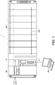
- FIG. 1 is a schematic view illustrating an example of the configuration of the PLC system 1 to which the support device 300 according to this embodiment can be applied.
- the PLC system 1 will be described with reference to Fig. 1 .
- the PLC system 1 is an example of a control system for controlling control targets such as facilities, devices, and the like and automating a production process.
- the PLC system 1 includes a CPU unit 10, a power supply unit 100, and an input/output (I/O) unit 200.
- the CPU unit 10 is a subject that executes various programs including a control program.
- the CPU unit 10 includes a universal serial bus (USB) interface 51 that can be connected to the support device 300.
- the CPU unit 10 exchanges data with the support device 300 through the USB interface 51.
- the power supply unit 100 converts a voltage of an input power input from the outside and supplies power to the CPU unit 10 and the I/O unit 200.
- the I/O unit 200 is connected to the CPU unit 10 through a system bus 202, exchanges signals with the CPU unit 10, and exchanges signals from the field.
- the support device 300 is a device that supports development of a control program executed by the PLC system 1.
- the support device 300 has a function for providing an environment for developing user programs including a control program executed by the PLC system 1, a function for setting the control program and various kinds of information in the PLC system 1, a function for acquiring a state value of the PLC system 1 during operation, and the like.
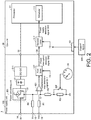
- Fig. 2 is a diagram illustrating an example of a situation in which settings of the power supply unit 100 and the CPU unit 10 according to this embodiment are applied.
- the power supply unit 100 receives input power input from the outside through an input terminal 14.
- the power received through the input terminal 14 is supplied to a rectification circuit 21.
- the rectification circuit 21 supplies power after full wave rectification to a power converting unit 201.
- the power converting unit 201 converts a voltage of supplied power.
- a part of an input power is charged into a capacitor 27 of the power converting unit 201, and the remainder of the input power is voltage converted by a DC/DC converter 211.
- the power converting unit 201 supplies the power after the conversion to the CPU unit 10 through an output terminal 32.
- the CPU unit 10 is driven by the voltage (for example, 5 V) of the supplied power.
- an input voltage is also supplied to a non-inverting input terminal of a comparator 421 through the power converting unit 201.
- a control voltage Vcc (for example, 5 V), which is input through an input terminal 18, is input to an inverting input terminal of the comparator 421.
- the control voltage Vcc (for example, 5 V) is divided by a resistor R1 and a resistor R2 connected in series through an input terminal 19 and is input to the inverting input terminal of the comparator 421 as a threshold voltage Vn (for example, 2.5 V).
- resistor R3 One end of the resistor R3 is connected to the resistor R2 in series, and the other end is grounded.
- a switch SW is connected to the resistor R3 in parallel.
- a voltage based on the control voltage Vcc is divided by the resistor R1 and the resistor R2 when the switch SW is on. In other words, when the switch SW is on, the resistor R3 forms a short circuit, and a resistance value thereof substantially becomes 0 ⁇ .
- the comparator 421 compares an amplitude value (for example, 0 to 5 V) of an input voltage input to the inverting input terminal with the threshold voltage Vn input to the non-inverting input terminal and, in a case in which the amplitude value becomes lower than the threshold voltage Vn, outputs an instantaneous stop detection signal SN1 that is a signal indicating that a predetermined voltage will not be supplied to the power supply unit 100.
- an amplitude value for example, 0 to 5 V
- the threshold voltage Vn remains a value that has been previously set without any change (for example, in the case of being a fixed value of 2.5 V)
- the instantaneous stop detection signal SN1 is repeatedly output from the comparator 421 in a short time, and a frequency at which the PLC system 1 ends the operation based on this signal increases.
- the operation rate of the PLC system 1 may decrease in this way.
- a decrease in the operation rate can be prevented as well.
- the setting of the threshold voltage Vn can be changed by an external operation on the power supply unit 100. More specifically, by a user operating a changeover switch 26 disposed on the surface of a casing of the power supply unit 100, the setting of the threshold voltage Vn is changed. Due to a user operating the changeover switch 26, the resistance value of the resistor R3 changes. For example, in a case in which the switch SW is on, the resistor R3 forms a short circuit. On the other hand, in a case in which the switch SW is off, the resistor R3 does not form a short circuit, and the control voltage Vcc is divided to the resistor R1, the resistor R2, and the resistor R3.
- the threshold voltage Vn is made lower than that of a case in which the switch SW is off. In this way, a frequency at which the amplitude value becomes smaller than the threshold voltage Vn is low in the PLC system 1, and a decrease in the operation efficiency of the system can be prevented.
- an instantaneous stop detection signal SN1 is output from an output terminal of the comparator 421 to a first timer 127.
- the first timer 127 measures a time over which the amplitude value has been lower than the threshold voltage Vn, and the state has continued.
- the first timer 127 outputs a power interruption detection signal SN2.
- the power interruption detection signal SN2 is input to a second timer 117 of the CPU unit 10 through an output terminal 34.
- the power interruption detection signal SN2 is a signal used for notifying that predetermined power cannot be supplied from the power supply unit 100 to the CPU unit 10.
- the second timer 117 measures a time over which a state, in which the amplitude value is lower than the threshold voltage Vn, has continued after receiving the power interruption detection signal SN2. In a case in which it is detected that the measured time is over a time T2 set in advance, the second timer 117 outputs a power supply detection signal SN3 to the processor 11.
- the time T2 as will be described below, is a time that can be adjusted by a user operation.
- the time T2 will be referred to as an adjustment time T2.
- the processor 11 is driven using a voltage (for example, 5 V) of power supplied from the output terminal 32 of the power supply unit 100.
- the processor 11 executes various processes of the CPU unit 10 by expanding and executing various programs recorded in a storage (a storage 150 illustrated in Fig. 5 to be described below). More specifically, the processor 11 executes a scheduler 111.
- the scheduler 111 determines an execution sequence, execution interruption, and the like of a plurality of processes in accordance with a control period set in advance. More specifically, the scheduler 111 allocates processing resources to a control program execution process, peripheral processes including various processes, and input/output processes in accordance with a priority level, a control period, and the like set in advance.
- the scheduler 111 causes the processor 11 to continue execution of a normal arithmetic operation process (normal process) during the adjustment time T2.
- Normal processes for example, refer to processes of tasks that are periodically executed, interrupt tasks, and the like and refer to processes other than tasks that are in preparation for stopping of the supply of power.
- the scheduler 111 causes the processor 11 to execute pre-stop processing in preparation for stopping of supply of power to the PLC system 1 in place of an arithmetic operation process that is currently being executed. More specifically, the scheduler 111 causes the processor 11 to execute a process of saving data during execution of a process in a memory card (for example, a memory card 178 illustrated in Fig. 5 ) or the like.
- the PLC system 1 stops after the comparator 421 outputs the instantaneous stop detection signal SN1, the PLC system 1 is driven using power charged into the capacitor 27.
- the threshold voltage Vn of the comparator 421 of the power supply unit 100 is set, for example, to be lower than 2.5 V, when a frequency of detection of stopping of supply of power decreases, an output timing of the instantaneous stop detection signal SN1 is delayed compared with that of a case in which the threshold voltage Vn is set to 2.5 V.
- a voltage charged into the capacitor 27 becomes lower than that before the output timing of the instantaneous stop detection signal SN1 was delayed (when the threshold voltage Vn is 2.5 V), and a time in which the PLC system 1 can operate after the output timing of the instantaneous stop detection signal SN1 is shortened. More specifically, a total time of the time T1 until the first timer 127 outputs the power interruption detection signal SN2, an adjustment time T2 until the second timer 117 outputs the power supply detection signal SN3, and a time in which pre-stop processing is executed is shortened.
- the time T1 (for example, 10 sec) is a constant time
- the time of the pre-stop processing for example, 5 sec
- the length of the adjustment time T2 needs to be shortened (For example, 10 sec -> 5 sec).
- the setting of the adjustment time T2 can be changed by an external operation on the CPU unit 10. More specifically, the setting of the adjustment time T2 is changed by a user operating the support device 300 that is electrically connected through the USB interface 51 of the CPU unit. For example, a user can change the time of the previous-time setting of the adjustment time T2 to a time shorter than the time by operating an input unit such as a keyboard, a mouse, or the like of the support device 300. In this way, a user can set the adjustment time T2 to an arbitrary time.
- the PLC system 1 can decrease a frequency at which the operation of the system ends in due to stopping of supply of power, and an execution time of pre-stop processing in preparation for stopping of supply of power can be reliably secured by changing the threshold voltage Vn and the adjustment time T2.
- information relating to the adjustment time T2 is stored in the storage 150 illustrated in Fig. 5 to be described below as setting information 154.
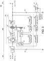
- Fig. 3 is a diagram illustrating an example of the circuit configuration of the power supply unit 100 according to this embodiment.
- the power supply unit 100 for example, is a switching power supply device.
- the power supply unit 100 includes an input unit 10A, a power supply unit 20B, and an output unit 30C.
- the input unit 10A is connected to an AC power supply (for example, a commercial power supply of 50 Hz/60 Hz, 100 V/200 V).
- the input unit 10A includes an input terminal 14 and a fuse 55 connected to the input terminal 14.
- the fuse 55 is an example of a protection circuit according to this embodiment.
- the power supply unit 20B generates power used for driving the CPU unit 10 based on power input from the input unit 10A.
- the power supply unit 20B includes a rectification circuit 21, a transformer 22, a MOSFET 23 as a switching device, a rectification smoothing circuit 24, a noise filter 25, a capacitor 27, a drive control circuit 28, an overcurrent detecting circuit 29, an AC amplitude detecting circuit 40, a voltage detecting circuit 41, an instantaneous stop detecting circuit 42, a photo coupler 43, a photo coupler 44, a capacitor 45, and a capacitor 46.
- the power converting unit 201 of the power supply unit 20B there are the rectification circuit 21, the transformer 22, the MOSFET 23, the rectification smoothing circuit 24, the capacitor 27, the drive control circuit 28, the overcurrent detecting circuit 29, the voltage detecting circuit 41, and the photo coupler 43.
- the DC/DC converter 211 there are remaining circuits and the like when the rectification circuit 21 and the capacitor 27 included in the power converting unit 201 are excluded.
- the noise filter 25 performs filtering for a high-frequency noise component superimposed in an AC voltage input to INPUT and supplies an AC voltage from which the noise component has been eliminated to the rectification circuit 21.
- the capacitor 27 is charged using a voltage after full-wave rectification and supplies the charged voltage to the transformer 22. More specifically, the capacitor 27 is charged using a part of the voltage after full-wave rectification, smooths the remaining voltage, and supplies a resultant voltage to the transformer 22.
- the rectification circuit 21 supplies the voltage after full-wave rectification also to the AC amplitude detecting circuit 40 together with the capacitor 27.
- the transformer 22 includes a primary winding 22p, a secondary winding 22s, and an auxiliary winding 22a and induces a high-frequency pulse voltage generated in the primary winding 22p in the secondary winding 22s and the auxiliary winding 22a.
- the high-frequency pulse voltage induced in the secondary winding 22s is used for DC output, and the high-frequency pulse voltage induced in the auxiliary winding 22a is used for operating the drive control circuit 28.
- the rectification smoothing circuit 24 is composed of a half-wave rectification circuit of a diode and a capacitor, performs half-wave rectification and then smoothing on a high-frequency pulse voltage induced in the secondary winding 22s of the transformer 22, and generates power of a DC output having a predetermined output voltage and a predetermined output current.
- the voltage detecting circuit 41 detects a DC voltage.
- the photo coupler 43 outputs a signal corresponding to the detected voltage to the drive control circuit 28.
- the drive control circuit 28 is configured by a control IC including a pulse width modulation (PWM) signal generator, a feedback control circuit, an over current protect (OCP) terminal, a switching driving terminal, a driving power supply terminal, and the like.
- the drive control circuit 28 drives the MOSFET 23 by supplying a PWM signal to a gate of the MOSFET 23.
- a secondary-side voltage detected by the voltage detecting circuit 41 is fed back to the drive control circuit 28 through the photo coupler 43.
- the drive control circuit 28 changes a duty ratio of the PWM signal based on the fed back voltage and drives the MOSFET 23 such that an output voltage becomes a predetermined voltage.
- the MOSFET 23 is connected to the primary winding 22p of the transformer 22 in series.
- the MOSFET 23 turns off/on a primary-side voltage in response to a PWM signal supplied from the drive control circuit 28, thereby generating a high-frequency pulse voltage in the primary winding 22p of the transformer 22.
- a voltage generated by the power supply unit 20B is output from the output unit 30C.
- the output unit 30C outputs a voltage generated by the power supply unit 20B.
- the output unit 30C includes an output terminal 32 (DC OUTPUT). In the configuration illustrated in Fig. 3 , a DC voltage is output as an output voltage.
- the rectification circuit 21 supplies a voltage after full-wave rectification to the AC amplitude detecting circuit 40.
- the AC amplitude detecting circuit 40 outputs an input voltage to the instantaneous stop detecting circuit 42 through the photo coupler 44.
- the instantaneous stop detecting circuit 42 outputs the input voltage to the first timer 127.
- the first timer 127 outputs the instantaneous stop detection signal SN1 to the CPU unit 10 through the output terminal 34.
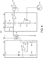
- Fig. 4 is a diagram illustrating an example of the circuit configuration of the AC amplitude detecting circuit 40 and the instantaneous stop detecting circuit 42 according to this embodiment.
- the AC amplitude detecting circuit 40 is a circuit that detects a magnitude (amplitude value) of a signal relating to the voltage VIN that has been full-wave rectified by the rectification circuit 21.
- the AC amplitude detecting circuit 40 includes a Zener diode 401, an operational amplifier 402, a transistor 403, a resistor R11, and a resistor R12.
- the Zener diode 401 has a cathode connected to an input terminal 16 and an anode connected to a non-inverting input terminal of the operational amplifier 402 through a node a.
- the anode of the Zener diode 401 is connected to one end of the resistor R11 in series through the node a. The other end of the resistor R11 is grounded.
- a voltage VIN is input to the non-inverting input terminal of the operational amplifier 402 through the node a.
- An output signal from an output terminal of the operational amplifier 402 is fed back and is input to the inverting input terminal of the operational amplifier 402.
- an output signal from the operational amplifier 402 is input to a base of the transistor 403, and the transistor 403 comes into an on state.
- a control voltage Vdd (for example, 5 V) supplied to the input terminal 17 is input to the inverting input terminal through a node b.
- a voltage (amplitude value) based on an output voltage of the operational amplifier 402 is input to a non-inverting input terminal of the comparator 421 of the instantaneous stop detecting circuit 42 through the photo coupler 44 that has amplified the voltage.
- the instantaneous stop detecting circuit 42 includes a comparator 421, a resistor R1, a resistor R2, a resistor R3, a resistor R4, and a switch SW.
- a voltage in the range of 0 to 5 V based on the control voltage Vcc (for example, 5 V) supplied using the input terminal 18 is input to the non-inverting input terminal of the comparator 421 through the resistor R4.
- the resistor R4 is a pull up resistor that raises the voltage of the non-inverting input terminal.
- a voltage based on the control voltage Vcc (for example, 5 V) supplied to the input terminal 19 is input to the non-inverting input terminal of the comparator 421. More specifically, a voltage acquired by dividing the control voltage Vcc input to the input terminal 19 by the resistors R1 and R2 is input to the inverting input terminal though a node c.
- the node c is disposed between the resistor R1 and the resistor R2 connected in series.
- the control voltage Vcc is divided by the resistor R1 and the resistor R2 when the resistor R3 connected to the resistor R2 in series forms a short circuit, and a resistance value thereof substantially becomes 0 ⁇ . In other words, this is in a case in which the switch SW disposed in parallel with the resistor R3 is in the on state. In a case in which the switch SW is in an off state, the control voltage Vcc is divided by the resistor R1, the resistor R2, and the resistor R3.
- a voltage (threshold voltage) input to the inverting input terminal of the comparator 421 is lower than that of the case of the off state.
- a state in which the voltage is equal to or lower than the threshold voltage Vn is relatively short, and thus, a frequency at which the instantaneous stop detection signal SN1 is output from the output terminal of the comparator 421 to the first timer 127 decreases.
- the power interruption detection signal SN2 is not frequently input to the CPU unit 10, and the PLC system 1 does not frequently stop, and accordingly, a decrease in the operation rate of the PLC system 1 can be prevented.
- the on/off switching of the switch SW is performed by an external operation on the changeover switch 26.
- the setting of the threshold voltage Vn of the comparator 421 can be changed by an external operation using the changeover switch 26.
- the changeover switch 26, for example, is a DIP switch, a rotary switch, or the like.
- the changeover switch 26, for example, is disposed on the surface of the power supply unit 100. In this way, the power supply unit 100 can easily receive change of the threshold voltage Vn using a user's manual operation. In addition, a user can easily change the threshold voltage Vn.
- the number of resistors connected to the resistor R2 in series is assumed to be one (the resistor R3), and the number of switches connected to the resistor R3 in parallel is assumed to be one (the switch SW).
- the number of resistors connected to the resistor R2 in series may be two or more.
- a switch may be disposed in parallel with each of the resistors.
- a switch may be disposed in parallel with each of the three resistors.
- the threshold voltage Vn can be set to a more fine value.
- Fig. 5 is a diagram illustrating an example of the hardware configuration of the CPU unit 10 according to this embodiment.
- the CPU unit 10 is an arithmetic operation processing unit and includes a processor 11, a second timer 117, a third timer 118, a power supply circuit 120, a chip set 130, a storage 150, a main memory 161, an internal bus controller 162, a high-rank network controller 163, a field network controller 165, a USB controller 180, and a memory card controller 190.
- the processor 11 is composed of a central processing unit (CPU), a micro processing unit (MPU), a graphics processing unit (GPU), and the like.
- the processor 11 may employ a configuration having a plurality of cores, and a plurality of processors 11 may be disposed.
- the CPU unit 10 includes one or a plurality of processors 11 and/or a processor 11 including one or a plurality of cores.
- the chip set 130 realizes the process of the CPU unit 10 as a whole by controlling the processor 11 and peripheral elements.
- the storage 150 for example, is configured by a nonvolatile memory device such as a hard disk drive (HDD) or a solid state drive (SSD) or the like.
- the main memory 161 is configured by a volatile memory device such as a dynamic random access memory (DRAM) or a static random access memory (SRAM) or the like.
- DRAM dynamic random access memory
- SRAM static random access memory
- the processor 11 reads various programs stored in the storage 150 and expands and executes the programs in the main memory 161, thereby realizing control and various processes corresponding to control targets.
- a sequence program 152 in addition to a system program 153 for realizing basic functions, a sequence program 152, a user program 151, and setting information 154 generated in accordance with a manufacturing apparatus and facilities that are control targets are stored.
- the system program 153 is a software group used for providing functions of the CPU unit 10. More specifically, the system program 153 includes a scheduler program and other system programs.
- the sequence program 152 is entirely scanned for each execution and has a concept including a program that can output a control instruction for each execution.
- a sequence command and/or a motion command may be included. Basically, the sequence program 152 is arbitrarily generated by a user in accordance with a control target and an application.
- the user program 151 is generated based on a user's purpose of control.
- the user program is a program that is arbitrarily designed in accordance with a target line (process) or the like controlled using the PLC system 1.
- the user program 151 realizes a user's purpose of control in cooperation with the sequence program 152.
- the user program 151 realizes a programmed operation by using a command, a function, a functional module, and the like provided by the sequence program 152.
- the setting information 154 includes information that defines a configuration and settings of the PLC system 1 including the CPU unit 10.
- the setting information includes measurement times of the first timer 127, the second timer 117, and the third timer 118. More specifically, the setting information 154 includes information of a time T1, an adjustment time T2, and a time T5 that are times to be measured by the timers.
- the setting information 154 includes information of a user program and setting values associated with a field device 172 connected to a field network N2 and information of a user program and setting values associated with a device connected to a high-rank network N1.
- the high-rank network controller 163 controls exchange of data with other devices such as a server apparatus and the like through the high-rank network N1.
- the internal bus controller 162 controls exchange of data with the I/O unit 200 installed in the CPU unit 10. More specifically, the internal bus controller 162 functions as a transmission buffer of data (output data) output to the I/O unit 200 and a reception buffer of data (input data) input from the I/O unit 200. In addition, output data generated by an arithmetic operation process of the processor 11 is stored in the storage 150. Output data to be transmitted to a specific I/O unit 200 is read from the storage 150 and is temporarily stored in the transmission buffer. In addition, input data transmitted from the I/O unit 200 is temporarily stored in the reception buffer and then is moved to the storage 150.
- the internal bus controller 162 performs a process of transmitting output data of the transmission buffer and a process of receiving input data and storing the input data in the reception buffer for the I/O unit 200.
- the internal bus controller 162 provides functions of a physical layer and a data link layer in an internal bus.
- the field network controller 165 controls exchange of data with the field device 172 through the field network N2.
- the field network controller 165 controls transmission of output data and reception of input data in accordance with the specifications of the field network N2. More specifically, the field network controller 165 functions as a transmission buffer of data (output data) output to the field device 172 and a reception buffer of data (input data) input from the field device 172.
- the output data generated by an arithmetic operation process using the processor 11 is stored in the storage 150.
- Output data to be transmitted to a specific field device 172 is read from the storage 150 and is temporarily stored in the transmission buffer.
- input data transmitted from the field device 172 is temporarily stored in the reception buffer and then is moved to the storage 150.
- the field network controller 165 performs a process of transmitting output data of the transmission buffer and a process of receiving input data and storing the input data in the reception buffer for the field device 172.
- the field network controller 165 provides functions of a physical layer and a data link layer in the field network N2.
- the power supply circuit 120 supplies power acquired through the output terminal 32 of the power supply unit 100 to the processor 11.
- the second timer 117 measures a time over which a state, in which the amplitude value is lower than the threshold voltage Vn, has continued after start of reception of the power interruption detection signal SN2 from the first timer 127 through the output terminal 34. In a case in which it is detected that the measured time is over the adjustment time T2 set in advance, the second timer 117 outputs the power supply detection signal SN3 to the processor 11 through the chip set 130.
- the processor 11 When the power supply detection signal SN3 is received, the processor 11 operates the scheduler 111.
- the scheduler 111 determines an execution sequence, an execution interruption, and the like of a plurality of processes in accordance with a control period set in advance.
- the scheduler 111 allocates process resources (a processor time, a memory, and the like) to a control program execution process, peripheral processes including various processes, and an input/output process in accordance with priority levels, control periods, and the like set in advance. More specifically, when the power supply detection signal SN3 is received, the scheduler 111 executes not a process relating to stopping of supply of power but a normal arithmetic operation process during the adjustment time T2.
- the scheduler 111 executes pre-stop processing in place of a normal arithmetic operation process (normal process) that is being currently executed.
- data is input to the memory card controller 190 through a memory card interface 52.
- the memory card controller 190 controls exchange of data with the memory card 178.
- the processor 11 writes data during execution of the process into the memory card 178 under control of the memory card controller 190, thereby executing pre-stop processing for temporarily saving the data from the CPU unit 10.
- the CPU unit 10 is configured such that the memory card 178 can be installed or uninstalled in this way and can record data in the memory card 178 and read various kinds of data from the memory card 178.
- the adjustment time T2 set in the second timer 117 is changed by an external operation on the CPU unit 10. More specifically, when a user operates the support device 300, data is input to the USB controller 180 through the USB interface 51 that is electrically connected to the support device 300. In this way, the USB controller 180 controls exchange of data with the support device 300 through the USB interface 51.
- the processor 11 executes a process by receiving information input by a user using the support device 300 through the USB interface 51. In this way, by configuring the setting of the adjustment time T2 to be changeable, after supply of power is stopped, the PLC system 1 can reliably execute a process in preparation for stopping of supply of power in place of the arithmetic operation process that is currently being executed.
- the third timer 118 receives a power interruption detection signal SN2 output from the first timer 127 through the output terminal 32.
- the third timer 118 measures a time until the arithmetic operation of the CPU unit 10 ends after start of reception of the power interruption detection signal SN2.
- the third timer 118 outputs a stop instruction signal SN4 to the processor 11 through the chip set 130.
- This stop instruction signal SN4 is a signal for stopping the execution of a program of the processor 11 and ending the operation of the PLC system 1.
- the PLC system 1 can end the operation of the system at an appropriate timing corresponding to a remaining power after stopping of the supply of power.
- the time T5 is a time that includes the adjustment time T2
- the length of this time T5 is also changed.
- the length of the adjustment time T2 is changed such that the pre-stop processing is completed before the operation of the PLC system 1 ends.
- the length of the adjustment time T2 is changed such that the pre-stop processing ends before the time T5 elapses. In this way, by adjusting the adjustment time T2 included in the time T5, even after the supply of power is stopped, the PLC system 1 is caused to end the operation of the system after a necessary process is completed.
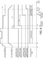
- Fig. 6 is a timing diagram illustrating a process in a case in which the threshold voltage Vn, the adjustment time T2, and the time T5 according to this embodiment have values set at a previous time (a previous-time setting value).
- a previous-time setting value of the threshold voltage will be described as Vs
- a previous-time setting value of the adjustment time T2 will be described as T2s
- a previous-time setting value of the time T5 will be described as T5s.
- the horizontal axis represents the time (msec)
- the vertical axis represents an AC input voltage (V), a DC output voltage (V), an instantaneous stop detection signal SN1, a power interruption detection signal SN2, a power supply detection signal SN3, a stop instruction signal SN4, and a program execution state.
- the AC input voltage represents a voltage value of a voltage input to the non-inverting input terminal of the comparator 421 of the power supply unit 100.
- the DC output voltage represents a voltage value of a voltage output from the output terminal 32.
- the instantaneous stop detection signal SN1 is a signal (high signal) that is output from the output terminal of the comparator 421 in a case in which the AC input voltage input to the non-inverting input terminal of the comparator 421 is lower than a threshold voltage Vs.
- the power interruption detection signal SN2 is a signal (high signal) that is output at a timing at which the time T1 set in advance has elapsed from a timing at which the input of the instantaneous stop detection signal SN1 was received by the first timer 127.
- the power supply detection signal SN3 is a signal (high signal) that is output at a timing at which an adjustment time T2s set in advance has elapsed from a timing at which the second timer 117 started to receive the power interruption detection signal SN2.
- the stop instruction signal SN4 is a signal (high signal) that is output at a timing at which a time T5s has elapsed from a timing at which the third timer 118 started to receive the power interruption detection signal SN2.
- a normal task is a task that is periodically executed, or an interrupt task other than a task that is executed with priority in accordance with stop of the power supply.
- the instantaneous stop detection signal SN1 is output from the output terminal of the comparator 421 to the first timer 127 (a high signal).
- the first timer 127 outputs the power interruption detection signal SN2 to the second timer 117 of the CPU unit 10 (a high signal).
- the second timer 117 outputs the power supply detection signal SN3 to the processor 11 (a high signal).
- the processor 11 executes pre-stop processing in place of the arithmetic operation process that is being currently executed. More specifically, the scheduler 111 performs an interrupt process for a normal arithmetic operation process that is being currently executed and executes pre-stop processing.
- the third timer 118 After a spare time T4 (a time t8 to a time t9) elapses before the PLC system 1 stops after the end of the pre-stop processing, the third timer 118 outputs the stop instruction signal SN4 (a high signal). In accordance with the output of the stop instruction signal SN4, the PLC system 1 ends the operation. In this way, when the AC input voltage becomes lower than the threshold voltage Vs, the instantaneous stop detection signal SN1 is output from the output terminal of the comparator 421. When the state in which the AC input voltage is lower than the threshold voltage Vs continues, and, after a time T1 set in advance elapses, and a time T5s further elapses, the PLC system 1 ends the operation. In addition, the time T5s is a time including the adjustment time T2s, the time T3, and the spare time T4.
- Fig. 7 is a timing diagram illustrating a process in a case in which the threshold voltage Vn, the adjustment time T2, and the time T5 according to this embodiment have been changed from the previous-time setting values.
- the threshold voltage after change will be described as Va
- the adjustment time T2 after change will be described as an adjustment time T2a
- a time T5 after change will be described as a time T5a.
- the threshold voltage Va is a voltage lower than Vs.
- the adjustment time T2a is a time shorter than the adjustment time T2s.
- the time T5a is a time shorter than the time T5s.
- a timing at which the comparator 421 outputs the instantaneous stop detection signal SN1 becomes a time t4.
- the timing becomes a time that is later than the time t2 described with reference to Fig. 6 .
- the time T3 of the pre-stop processing (an execution time T3), and the time T4 (the spare time T4) are times of lengths that are the same as those illustrated in Figs.
- the adjustment time T2s needs to be changed to a shorter time.
- the change of the adjustment time T2s is realized by user's setting using the support device 300.
- a user changes the adjustment time T2s to a shorter time T2a using the support device 300.
- the processor 11 executes pre-stop processing during a time T3 (a time t7 to a time t10) after elapse of the adjustment time T2a (a time t5 to a time t7).
- the PLC system 1 ends the operation after elapse of a time T4 (a time t10 to a time t11).
- the time T5a is a time that includes the adjustment time T2a, the time T3, and the time T4. For this reason, the time T5a is a time that is shorter than the time T5s.
- Fig. 8 is a schematic view illustrating an example of the hardware configuration of the support device 300 that is applied to the PLC system 1 according to this embodiment.
- the support device 300 typically, is configured by a general computer.
- the support device 300 may be provided in the form of a laptop personal computer having superior portability.
- the support device 300 includes a CPU 302 that executes various programs including an operating system (OS), a read only memory (ROM) 304 that stores a BIOS and various kinds of data, a memory RAM 306 that provides a work area used for storing data, which is necessary for executing a program in the CPU 302, and a hard disk (HDD) 308 that stores a program and the like executed by the CPU 302 in a nonvolatile manner.
- the support device 300 includes a keyboard 310 and a mouse 312 that receive operations from a user and a display 314 that is used for presenting information to the user.
- the support device 300 includes a communication interface 318 used for communicating with the CPU unit 10, the power supply unit 100, and the like.
- the support device 300 includes a recording media reading device 317 that is used for reading a support program from a recording medium 350 stored therein.
- a user can change the setting of the adjustment time T2 using input units such as the keyboard 310, the mouse 312, and the like of the support device 300.
- input units such as the keyboard 310, the mouse 312, and the like of the support device 300.
- the adjustment time T2s also needs to be shortened.
- An example of calculation equations for calculating values of the threshold voltage Vn and the adjustment time T2 will be described below.
- Tm 1 / 2 ⁇ C ⁇ V 2 / P
- C Capacitance of the capacitor 27
- V Voltage of the capacitor 27
- P Power consumption of a device including the CPU unit 10 connected to the output terminal 32.
- Equation (2) In a case in which the threshold voltage Vn and the adjustment time T2 are set to Vs and Ts of the previous-time setting values from Equation (1), and a maintaining time Th based on these values is set to a standard maintaining time Ths based on the previous-time setting values, Equation (2) is satisfied.
- Wmax Maximum rated power of the power supply unit 100
- Vs Previous-time setting value of the threshold voltage Vn (the threshold voltage Vn before change).
- settings of a plurality of stages including Vb, Vc, and Vd and the threshold voltage Vs can be changed.
- Fig. 9 is a diagram illustrating an example of change of a voltage setting of the threshold voltage Vn according to this embodiment.
- switches switches SWa, SWb, SWc, and SWd
- resistors resistors R3a, R3b, R3c, and R3d
- Part (B) of Fig. 9 illustrates changes in the threshold voltage Vn corresponding to on/off of the switches SWa to SWd. More specifically, in a case in which resistance values of the resistors R3a, Rb, Rc, and R3d are configured to be the same resistance values, when all the switches are off (the switches SWa, SWb, SWc, and SWd are off), a total resistance value of such resistors becomes a maximum. As a result, the threshold voltage becomes a largest threshold voltage (for example, Vs). As the number of switches that are set to on among the switches SWa, SWb, SWc, and SWd becomes larger, the threshold voltage decreases.
- the threshold voltage becomes the threshold voltage Vd and becomes a threshold voltage lower than the other threshold voltages (for example, Va, Vb, and Vc).
- the changeover switch 26, for example, is a rotary switch, and, by switching the switch to one of numbers 0 to 9, the threshold voltage Vn can be set to one of a plurality of voltages. For example, the threshold voltage can be changed from a large voltage Vn to a low voltage (Vs > Va > Vb > Vc > Vd).
- the values of the threshold voltage Vn and the adjustment time T2 are selected such that a condition represented in Equation (4) is satisfied based on Equation (2) and Equation (3). Ths ⁇ Tha ⁇ T 2 + T 4
- the threshold voltage Vn and the adjustment time T2 are set such that a value acquired by subtracting the maintaining time Tha after change from the maintaining time Ths before change is smaller than a sum of the adjustment time T2 after change (for example, T2a) and the spare time T4.
- the threshold voltage Vn and the adjustment time T2 are associated with each other, and, in a case in which the setting of one thereof is changed, the setting of the other needs to be also changed in accordance with details of the change.
- a method of changing the setting for example, as described above, there is a method in which a user sets the threshold voltage Vn using the changeover switch 26 and changes the adjustment time T2 using the support device 300.
- a user may change the threshold voltage Vn and the adjustment time T2 using the support device 300.
- a switch similar to the changeover switch 26 also on the surface of the CPU unit 10 a user may change the threshold voltage Vn and the adjustment time T2 by operating the changeover switch 26 disposed in the power supply unit 100 and the switch disposed in the CPU unit 10.
- a user inputs a value after change of one of the threshold voltage Vn and the adjustment time T2 to the support device 300 using the input unit
- the CPU 302 calculates a value after change of the other by executing an arithmetic operation process, and the settings of the threshold voltage Vn and the adjustment time T2 are changed based on the value input by the user and the calculated value.
- Fig. 10 is a diagram illustrating an example of an image displayed in the display 314 in a case in which the support device 300 according to this embodiment calculates a threshold voltage Vn.
- a user inputs a maximum rated output (Wmax) of the power supply unit 100, maximum power consumption (W 0 ) of the entire PLC system 1, and an adjustment time T2 by operating the input unit of the support device 300.
- the CPU 302 of the support device 300 calculates a threshold voltage Vn by performing an arithmetic operation process based on Equations (2), (3), and (4).
- the power consumption of the entire PLC system 1 is maximum power that is actually used by the CPU unit 10 and the I/O unit 200.
- the maximum rated output of the power supply unit 100 and the maximum power consumption of the entire PLC system 1 are calculated in advance by the support device 300 based on information acquired from the PLC system 1 and is notified to a user.
- the threshold voltage Vs that is a previous-time setting value in Equation (2) or Equation (3), a maximum value Imax of a current flowing through the primary winding 22p, and the capacitance C of the capacitor 27 are also calculated in advance by the support device 300.
- the CPU 302 of the support device 300 calculates a threshold voltage Vn (for example, the threshold voltage Va) from the value of the adjustment time T2 (for example, the adjustment time Ta) such that the relationship of Equation (4) is satisfied.
- the value of the threshold voltage Vn calculated in this way is displayed in the display 314.
- the PLC system 1 can display the threshold voltage in the display 314, and a change of the setting of the threshold voltage Vn can be received from a user who has checked the threshold voltage Vn displayed in the display 314.
- a user can change the setting of the threshold voltage Vn while checking the threshold voltage Vn displayed in the display 314.
- Fig. 11 illustrates a correspondence relation between the threshold voltage Vn, an amount of charging in the capacitor 27, and the adjustment time T2 according to this embodiment.
- the amount of charging in the capacitor 27 becomes Ps.
- the adjustment time T2 for the amount of charging Ps becomes the adjustment time T2s.
- the PLC system 1 can set an optimal threshold voltage Vn based on the set adjustment time T2.
- the PLC system 1 can set an optimal adjustment time T2 based on the set threshold voltage Vn.
- the CPU 302 of the support device 300 may calculate a threshold voltage Vn (for example, the threshold voltage Va) based on an adjustment time T2 (for example, the adjustment time T2a) input by a user's operation using the input unit.
- the support device 300 outputs a change instruction signal relating to the input adjustment time T2a to the CPU unit 10 through the communication interface 318.
- the processor 11 of the CPU unit 10 changes the adjustment time T2 of the setting information 154 to the adjustment time T2a based on the change instruction signal relating to the received adjustment time T2.
- the support device 300 outputs a change instruction signal relating to the threshold voltage Va to the power supply unit 100 through the communication interface 318.
- This change instruction signal may be output from the support device 300 to the power supply unit 100 through the CPU unit 10.
- the power supply unit 100 performs on/off switching of the switch SW based on the change instruction signal relating to the received threshold voltage Vn. In accordance with this, the threshold voltage Vn is changed.
- the on/off control of the switch SW may be performed such that, when the change instruction signal is received, the processor 11 may read setting information of the threshold voltage Vn from the storage 150 and execute the process of changing the threshold voltage Vn.
- the threshold voltage Vn is stored in the setting information 154 of the storage 150 of the CPU unit 10 in advance.
- the process may be executed by the processor.
- the threshold voltage Vn is changed to a voltage lower than a voltage that has been set at the previous time.
- the threshold voltage Vn is changed to a voltage higher than a voltage that has been set at the previous time. In this way, the PLC system 1 can change the threshold voltage Vn in association with a change in the time T2 of the second timer 117, and user convenience at the time of changing the setting is improved.
- the adjustment time T2 by changing the adjustment time T2 to a time (for example, the adjustment time T2a) shorter than the adjustment time T2s that is the setting value of the previous time, a time in which the CPU unit 10 can operate after stop of the supply of power becomes shorter than that for the adjustment time T2 before change.
- the threshold voltage Vn by changing the threshold voltage Vn to a voltage (for example, the threshold voltage Va) lower than Vs that has been set at the previous time, a frequency at which stop of supply of power is determined decreases. In this way, the operation rate of the PLC system 1 is improved.
- the adjustment time T2 is changed from the adjustment time T2a that has been set at the previous time to another time (for example, the adjustment time T2s) (Ta ⁇ Ts)
- the adjustment time becomes longer than that before change, and thus, a voltage to be charged into the capacitor needs to be a voltage higher than that before change.
- the threshold voltage that has been set at the previous time is Va
- the threshold voltage Vn is changed to a voltage higher than that (for example, the threshold voltage Vs).
- the adjustment time T2 and the threshold voltage Vn of the PLC system 1 are changed in association with each other. In this way, the PLC system 1 can adjust a frequency at which stop of the supply of power is determined in accordance with the form of the system, and a necessary process after the determination of stop of the supply of power can be reliably executed.
- the CPU 302 of the support device 300 may calculate an adjustment time T2 (for example, the adjustment time T2a) based on a threshold voltage (for example, the threshold voltage Va) input from the input unit by a user.
- the support device 300 outputs a change instruction signal relating to the input threshold voltage Va to the power supply unit 100 through the communication interface 318.
- This change instruction signal may be output from the support device 300 to the power supply unit 100 through the CPU unit 10.
- the power supply unit 100 performs on/off switching of the switch SW based on the change instruction signal relating to the received threshold voltage Vn, whereby the threshold voltage Vn is changed.
- on/off control of the switch SW may be performed such that, when the change instruction signal is received, the processor 11 reads setting information of the threshold voltage Vn from the storage 150 and execute the process of changing the threshold voltage Vn.
- the threshold voltage Vn is stored in the setting information 154 of the storage 150 the CPU unit 10 in advance.
- a processor and a storage may be provided in the power supply unit 100, and the process may be executed by the processor.
- the support device 300 outputs the change instruction signal relating to the adjustment time T2a to the CPU unit 10 through the communication interface 318.
- the processor 11 of the CPU unit 10 changes the adjustment time T2 of the setting information 154 to the adjustment time T2a based on received the change instruction signal relating to the adjustment time T2.
- the adjustment time T2 is changed to a time shorter than that set at the previous time.
- the adjustment time T2 is changed to a time longer than that set at the previous time. In this way, the PLC system 1 can change the time T2 of the second timer 117 in association with a change of the threshold voltage Vn, and user's convenience at the time of performing a setting change is improved.
- the threshold voltage Vn to a voltage (for example, the threshold voltage Va) lower than the setting value Vs of the previous time
- a voltage charged into the capacitor 27 becomes lower than that at the time of the setting value Vs of the previous time.
- the operation time of the CPU unit 10 in a case in which the supply of power stops is shortened than that before the change of the threshold voltage Vn.
- the adjustment time T2 is changed to a time (for example, the adjustment time T2a) that is shorter than the setting value T2s of the previous time.
- the threshold voltage Vn is changed from Va that has been set at the previous time to another value (for example, the threshold voltage Vs) (Va ⁇ Vs)
- the voltage charged into the capacitor 27 becomes higher than that before the change.
- the operation time of the CPU unit 10 in a case in which the supply of power stops becomes longer than that before the change of the threshold voltage Vn.
- the adjustment time T2 is changed to a time (for example, the adjustment time T2s) that is longer than the adjustment time T2a that has been set at the previous time. In this way, the threshold voltage Vn and the adjustment time T2 of the PLC system 1 are changed in association with each other. In this way, the PLC system 1 can adjust a frequency at which the supply of power is determined to have stopped in accordance with the form of the system, and a necessary process after the determination of stop of the supply of power can be reliably executed.
- a dedicated hardware circuit for example, an ASIC, an FPGA, or the like.
- a main part of the CPU unit 10 may be realized using hardware (for example, an industrial PC based on a general computer) following a general architecture.
- OS operating systems
- a necessary application may be executed on each OS.
- the CPU unit 10 and the support device 300 are configured as separate bodies, a configuration in which all or some of functions of those are integrated in a single device may be employed.
- detection timings of the instantaneous stop detection signal SN1, the power interruption detection signal SN2, and the power supply detection signal SN3 illustrated in Figs. 6 and 7 and a CPU reset signal RS are set as switching timings from a low signal -> a high signal, switching timings from a high signal -> a low signal may be used.
- the timing diagrams illustrated in Figs. 6 and 7 are displayed on the display 314 of the support device 300, and a user may set the threshold voltage Vn and the adjustment time T2 by operating the changeover switch 26 while checking transitions of parameters such as the AC input voltage and the like in a time series.
- An embodiment of the present disclosure includes disclosures as below.
- a control system (1) including: a calculation unit (10) configured to execute an arithmetic operation process; and a power supply unit (100) configured to supply power to the calculation unit (10), the power supply unit (100) includes: a power converting unit (201) configured to use a part of an input power input from the outside for charging and convert a remainder of the input power into power supplied to the calculation unit (10); and a first detection unit (127) configured to compare a voltage of the input power with a threshold voltage and output a notification signal for notifying that predetermined power supply is not able to be performed in a case in which a time, over which a magnitude of the voltage has been lower than the threshold voltage, is detected to be over a first measurement time set in advance, the first detection unit (127) being configured to be able to change a setting of the threshold voltage by an external operation, and the calculation unit (10) includes: a second detection unit (117) configured to output an instruction signal for an instruction for execution of pre-stop processing in preparation for stopping of the predetermined power supply in a case in which it is
- control system described in Configuration 1 further including a third detection unit (118) configured to output a stop instruction signal in a case in which a third measurement time for ending the arithmetic operation process using the calculation unit (10) has elapsed.
- a switch that is able to change the setting of the threshold voltage by the external operation is disposed on a surface of the power supply unit (100).
- the threshold voltage is changed to a voltage lower than a voltage that has been set at a previous time in a case in which the second measurement time is changed to a time shorter than a time that has been set at a previous time, and the threshold voltage is changed to a voltage higher than a voltage that has been set at the previous time in a case in which the second measurement time is changed to a time longer than a time that has been set at the previous time.
- the second measurement time is changed to a time shorter than a time that has been set at the previous time in a case in which the threshold voltage is changed to a voltage lower than a voltage that has been set at a previous time, and the second measurement time is changed to a time longer than a time that has been set at a previous time in a case in which the threshold voltage is changed to a voltage higher than a voltage that has been set at the previous time.
- the control system according to any one of Configurations 1 to 5, further including a support device (300) configured to be electrically connected to the calculation unit (10), and the support device (300) includes: a calculation part (302) configured to calculate the threshold voltage corresponding to the second measurement time; and a display part (314) configured to display information relating to the threshold voltage.
- a power supply unit (100) that supplies power to a calculation unit (10) executing an arithmetic operation process
- the power supply unit including: a power converting unit (201) configured to use a part of an input power input from the outside for charging and convert a remainder of the input power into power supplied to the calculation unit (10); and a first detection unit (127) configured to compare a voltage of the input power with a threshold voltage and output a notification signal for notifying that predetermined power supply is not able to be performed in a case in which a time, over which a magnitude of the voltage has been lower than the threshold voltage, is detected to be over a first measurement time set in advance
- the calculation unit (10) is configured to receive the notification signal from the first detection unit (100), issue an execution signal for executing pre-stop processing in preparation for stopping of the predetermined power supply when a second measurement time set in advance has elapsed, continue to execute the arithmetic operation process during the second measurement time, execute the pre-stop processing in place of the arithmetic operation process that is
Landscapes
- Engineering & Computer Science (AREA)
- Physics & Mathematics (AREA)
- Theoretical Computer Science (AREA)
- General Physics & Mathematics (AREA)
- General Engineering & Computer Science (AREA)
- Nonlinear Science (AREA)
- Power Engineering (AREA)
- Automation & Control Theory (AREA)
- Programmable Controllers (AREA)
- Dc-Dc Converters (AREA)
- Power Sources (AREA)
Abstract
Description
- The present disclosure relates to a control system and, more particularly, relates to a process corresponding to stopping of supply of electric power.
- In production sites using factory automation (FA), industrial control systems such as a programmable logic controller (PLC), a robot controller, and the like have been introduced. A control system can automate a production process by controlling various industrial drive devices that can perform communication using a network. Relating to such a control system, in PCT Publication
WO 2005/088819 - Patent Literature 1: PCT Publication
WO 2005/088819 - In a case in which it is determined whether or not power supply has been stopped using an input voltage, a conventional control system compares a voltage value set in advance as a threshold voltage with an input voltage. For this reason, in a production site on which an input voltage frequently changes or the like, in a case in which a threshold voltage is set to be higher than a general value, a frequency at which a control system determines that power supply has been stopped and ends the operation of the system becomes high, and the operation rate of the system becomes low. In addition, in a case in which the threshold voltage is set to be lower than a general value, a frequency at which the control system determines that power supply has been stopped and ends execution of the system becomes low. However, a voltage charged into a capacitor of a control system based on an input voltage becomes lower than that at the time when the threshold voltage has a general value, and an execution time of pre-stop processing in preparation for stop of power supply becomes short, and there are cases in which the operation of the system cannot be appropriately ended. Therefore, a technology enabling determination of stop of supply of power to a control system to be performed at an appropriate timing and securement of an execution time of pre-stop processing is required.
- According to an embodiment of the present disclosure, a technology enabling determination of stop of supply of power to be performed at an appropriate timing and securement of an execution time of pre-stop processing is provided.
- A control system according to an embodiment of the present disclosure includes: a calculation unit that executes an arithmetic operation process; and a power supply unit that supplies power to the calculation unit. The power supply unit includes: a power converting unit that charges a part of an input power input from the outside for charging and converts a remainder of the input power into power supplied to the calculation unit; and a first detection unit that compares a voltage of the input power with a threshold voltage and outputs a notification signal for notifying that predetermined power supply is not able to be performed in a case in which a time, over which a magnitude of the voltage has been lower than the threshold voltage, is detected to be over a first measurement time set in advance, the first detection unit is able to change a setting of the threshold voltage by an external operation. The calculation unit includes: a second detection unit that outputs an instruction signal for an instruction for execution of pre-stop processing in preparation for stopping of the predetermined power supply in a case in which it is detected that a second measurement time set in advance has elapsed after receiving the notification signal; and a processing execution management unit that continues execution of the arithmetic operation process during the second measurement time and execute the pre-stop processing in place of the arithmetic operation process that is currently being executed after receiving the instruction signal, the second detection unit being configured to be able to change a setting of the second measurement time by an external operation.
- According to this configuration, by changing the threshold voltage and the adjustment time, the control system can decrease a frequency at which the operation of the system ends due to stopping of supply of power, and an execution time of pre-stop processing in preparation for stopping of supply of power can be reliably secured.
- The control system may further include a third detection unit that outputs a stop instruction signal in a case in which a third measurement time for ending the arithmetic operation process using the calculation unit has elapsed.
- According to this configuration, the control system can end the operation of the system at an appropriate timing according to a remaining power after stop of the supply of power.
- A switch that is able to change the setting of the threshold voltage by the external operation may be disposed on a surface of the power supply unit.
- According to this configuration, the control system can easily receive a change of the threshold voltage by a user's manual operation.
- In the first detection unit, the threshold voltage is changed to a voltage lower than a voltage that has been set at a previous time in a case in which the second measurement time is changed to a time shorter than a time that has been set at the previous time, and the threshold voltage is changed to a voltage higher than a voltage that has been set at a previous time in a case in which the second measurement time is changed to a time longer than a time that has been set at the previous time.
- According to this configuration, the control system can adjust a frequency at which it is determined that the supply of power is to be stopped by the form of the system, and a necessary process after the determination of stop of the supply of power can be reliably executed.
- In the second detection unit, the second measurement time may be changed to a time shorter than a time that has been set at a previous time in a case in which the threshold voltage is changed to a voltage lower than a voltage that has been set at the previous time, and the second measurement time may be changed to a time longer than a time that has been set at a previous time in a case in which the threshold voltage is changed to a voltage higher than a voltage that has been set at the previous time.
- According to this configuration, the control system can change a time of a second timer in association with a change of the threshold voltage, and user convenience at the time of changing the settings is improved.
- The control system may further include a support device configured to be electrically connected to the calculation unit. The support device includes: a calculation part that calculates the threshold voltage corresponding to the second measurement time; and a display part that displays information relating to the threshold voltage.
- According to this configuration, the control system can display the threshold voltage on the display and can receive a change of the setting from a user who has checked the threshold voltage displayed on the display.
- According to a yet another embodiment of the present disclosure, a power supply unit that supplies power to a calculation unit executing an arithmetic operation process is provided. The power supply unit includes: a power converting unit that changes a part of an input power input from the outside and converts a remainder of the input power into power supplied to the calculation unit; and a first detection unit that compares a voltage of the input power with a threshold voltage and outputs a notification signal for notifying that predetermined power supply is not able to be performed in a case in which a time, over which a magnitude of the voltage has been lower than the threshold voltage, is detected to be over a first measurement time set in advance. The calculation unit receives the notification signal from the first detection unit, issues an execution signal for executing pre-stop processing in preparation for stopping of the predetermined power supply when a second measurement time set in advance has elapsed, continues to execute the arithmetic operation process during the second measurement time, executes the pre-stop processing in place of the arithmetic operation process that is currently being executed after the execution signal is received, and is able to change a setting of the second measurement time by an external operation. The first detection unit is able to change the setting of the threshold voltage by an external operation.
- According to this configuration, by changing the threshold voltage and the adjustment time, the power supply unit can decrease a frequency at which the operation of the system ends due to stopping of supply of power, and an execution time of pre-stop processing in preparation for stopping of supply of power can be reliably secured.
- According to an embodiment of the present disclosure, determination of stop of supply of power can be performed at an appropriate timing, and an execution time of pre-stop processing can be secured.
-
-
Fig. 1 is a schematic view illustrating an example of the configuration of a PLC system to which a support device according to this embodiment can be applied. -
Fig. 2 is a diagram illustrating an example of a situation in which settings of a power supply unit and a CPU unit according to this embodiment are applied. -
Fig. 3 is a diagram illustrating an example of the circuit configuration of a power supply unit according to this embodiment. -
Fig. 4 is a diagram illustrating an example of the circuit configuration of an AC amplitude detecting circuit and an instantaneous stop detecting circuit according to this embodiment. -
Fig. 5 is a diagram illustrating an example of the hardware configuration of a CPU unit according to this embodiment. -
Fig. 6 is a timing diagram illustrating a process in a case in which a threshold voltage Vn, an adjustment time T2, and a time T5 according to this embodiment have values set at the previous time (a previous setting value). -
Fig. 7 is a timing diagram illustrating a process in a case in which the threshold voltage Vn, the adjustment time T2, and the time T5 according to this embodiment have been changed from the previous setting values. -
Fig. 8 is a schematic view illustrating an example of the hardware configuration of a support device that is applied to a PLC system according to this embodiment. -
Fig. 9 is a diagram illustrating an example of change of a voltage setting of a threshold voltage Vn according to this embodiment. -
Fig. 10 is a diagram illustrating an example of an image displayed in a display in a case in which a support device according to this embodiment calculates a threshold voltage Vn. -
Fig. 11 illustrates a correspondence relation between a threshold voltage Vn, an amount of charging in a capacitor, and an adjustment time T2 according to this embodiment. - Hereinafter, an embodiment of the present disclosure will be described with reference to the drawings. In the following description, the same reference signs will be assigned to components which are the same. In addition, names and functions thereof are the same. Thus, detailed description thereof will not be repeated.
- First, an example of the configuration of a
PLC system 1 to which asupport device 300 according to this embodiment can be applied will be described.Fig. 1 is a schematic view illustrating an example of the configuration of thePLC system 1 to which thesupport device 300 according to this embodiment can be applied. - The
PLC system 1 will be described with reference toFig. 1 . ThePLC system 1 is an example of a control system for controlling control targets such as facilities, devices, and the like and automating a production process. Typically, thePLC system 1 includes aCPU unit 10, apower supply unit 100, and an input/output (I/O)unit 200. TheCPU unit 10 is a subject that executes various programs including a control program. TheCPU unit 10 includes a universal serial bus (USB)interface 51 that can be connected to thesupport device 300. TheCPU unit 10 exchanges data with thesupport device 300 through theUSB interface 51. Thepower supply unit 100 converts a voltage of an input power input from the outside and supplies power to theCPU unit 10 and the I/O unit 200. The I/O unit 200 is connected to theCPU unit 10 through asystem bus 202, exchanges signals with theCPU unit 10, and exchanges signals from the field. - The
support device 300 is a device that supports development of a control program executed by thePLC system 1. Thesupport device 300 has a function for providing an environment for developing user programs including a control program executed by thePLC system 1, a function for setting the control program and various kinds of information in thePLC system 1, a function for acquiring a state value of thePLC system 1 during operation, and the like. - Next, an example of a situation in which the present disclosure is applied will be described with reference to
Fig. 2. Fig. 2 is a diagram illustrating an example of a situation in which settings of thepower supply unit 100 and theCPU unit 10 according to this embodiment are applied. In this embodiment, thepower supply unit 100 receives input power input from the outside through aninput terminal 14. The power received through theinput terminal 14 is supplied to arectification circuit 21. Therectification circuit 21 supplies power after full wave rectification to apower converting unit 201. Thepower converting unit 201 converts a voltage of supplied power. - A part of an input power is charged into a
capacitor 27 of thepower converting unit 201, and the remainder of the input power is voltage converted by a DC/DC converter 211. After changing the voltage of the supplied power, thepower converting unit 201 supplies the power after the conversion to theCPU unit 10 through anoutput terminal 32. TheCPU unit 10 is driven by the voltage (for example, 5 V) of the supplied power. - In addition, an input voltage is also supplied to a non-inverting input terminal of a
comparator 421 through thepower converting unit 201. A control voltage Vcc (for example, 5 V), which is input through aninput terminal 18, is input to an inverting input terminal of thecomparator 421. The control voltage Vcc (for example, 5 V) is divided by a resistor R1 and a resistor R2 connected in series through aninput terminal 19 and is input to the inverting input terminal of thecomparator 421 as a threshold voltage Vn (for example, 2.5 V). - One end of the resistor R3 is connected to the resistor R2 in series, and the other end is grounded. In addition, a switch SW is connected to the resistor R3 in parallel. A voltage based on the control voltage Vcc is divided by the resistor R1 and the resistor R2 when the switch SW is on. In other words, when the switch SW is on, the resistor R3 forms a short circuit, and a resistance value thereof substantially becomes 0 Ω. The
comparator 421 compares an amplitude value (for example, 0 to 5 V) of an input voltage input to the inverting input terminal with the threshold voltage Vn input to the non-inverting input terminal and, in a case in which the amplitude value becomes lower than the threshold voltage Vn, outputs an instantaneous stop detection signal SN1 that is a signal indicating that a predetermined voltage will not be supplied to thepower supply unit 100. - Here, in a case in which the threshold voltage Vn remains a value that has been previously set without any change (for example, in the case of being a fixed value of 2.5 V), in a production site or the like in which variations in a power supply voltage frequently occur, there are cases in which an amplitude value representing the magnitude of an input voltage frequently becomes below the threshold voltage Vn. As a result, the instantaneous stop detection signal SN1 is repeatedly output from the
comparator 421 in a short time, and a frequency at which thePLC system 1 ends the operation based on this signal increases. There is concern that the operation rate of thePLC system 1 may decrease in this way. In contrast to this, by changing the setting of the threshold voltage Vn, a decrease in the operation rate can be prevented as well. The setting of the threshold voltage Vn can be changed by an external operation on thepower supply unit 100. More specifically, by a user operating achangeover switch 26 disposed on the surface of a casing of thepower supply unit 100, the setting of the threshold voltage Vn is changed. Due to a user operating thechangeover switch 26, the resistance value of the resistor R3 changes. For example, in a case in which the switch SW is on, the resistor R3 forms a short circuit. On the other hand, in a case in which the switch SW is off, the resistor R3 does not form a short circuit, and the control voltage Vcc is divided to the resistor R1, the resistor R2, and the resistor R3. In this way, in a case in which the switch SW is on, the threshold voltage Vn is made lower than that of a case in which the switch SW is off. In this way, a frequency at which the amplitude value becomes smaller than the threshold voltage Vn is low in thePLC system 1, and a decrease in the operation efficiency of the system can be prevented. - In this way, in a case in which the set threshold voltage Vn is below the amplitude value of the input voltage, an instantaneous stop detection signal SN1 is output from an output terminal of the
comparator 421 to afirst timer 127. Thefirst timer 127 measures a time over which the amplitude value has been lower than the threshold voltage Vn, and the state has continued. In a case in which it is detected that the measured time is over a time T1 (for example, 10 seconds) set in advance, thefirst timer 127 outputs a power interruption detection signal SN2. The power interruption detection signal SN2 is input to asecond timer 117 of theCPU unit 10 through anoutput terminal 34. The power interruption detection signal SN2 is a signal used for notifying that predetermined power cannot be supplied from thepower supply unit 100 to theCPU unit 10. Thesecond timer 117 measures a time over which a state, in which the amplitude value is lower than the threshold voltage Vn, has continued after receiving the power interruption detection signal SN2. In a case in which it is detected that the measured time is over a time T2 set in advance, thesecond timer 117 outputs a power supply detection signal SN3 to theprocessor 11. The time T2, as will be described below, is a time that can be adjusted by a user operation. Hereinafter, the time T2 will be referred to as an adjustment time T2. - The
processor 11 is driven using a voltage (for example, 5 V) of power supplied from theoutput terminal 32 of thepower supply unit 100. Theprocessor 11 executes various processes of theCPU unit 10 by expanding and executing various programs recorded in a storage (astorage 150 illustrated inFig. 5 to be described below). More specifically, theprocessor 11 executes ascheduler 111. Thescheduler 111 determines an execution sequence, execution interruption, and the like of a plurality of processes in accordance with a control period set in advance. More specifically, thescheduler 111 allocates processing resources to a control program execution process, peripheral processes including various processes, and input/output processes in accordance with a priority level, a control period, and the like set in advance. For example, after the power interruption detection signal SN2 is input to thesecond timer 117, thescheduler 111 causes theprocessor 11 to continue execution of a normal arithmetic operation process (normal process) during the adjustment time T2. Normal processes, for example, refer to processes of tasks that are periodically executed, interrupt tasks, and the like and refer to processes other than tasks that are in preparation for stopping of the supply of power. Then, in a case in which a state in which the amplitude value is lower than the threshold voltage Vn continues even when the adjustment time T2 elapses, thescheduler 111 causes theprocessor 11 to execute pre-stop processing in preparation for stopping of supply of power to thePLC system 1 in place of an arithmetic operation process that is currently being executed. More specifically, thescheduler 111 causes theprocessor 11 to execute a process of saving data during execution of a process in a memory card (for example, amemory card 178 illustrated inFig. 5 ) or the like. - Here, until the
PLC system 1 stops after thecomparator 421 outputs the instantaneous stop detection signal SN1, thePLC system 1 is driven using power charged into thecapacitor 27. For this reason, in a case in which the threshold voltage Vn of thecomparator 421 of thepower supply unit 100 is set, for example, to be lower than 2.5 V, when a frequency of detection of stopping of supply of power decreases, an output timing of the instantaneous stop detection signal SN1 is delayed compared with that of a case in which the threshold voltage Vn is set to 2.5 V. In accordance with such a delay, a voltage charged into thecapacitor 27 becomes lower than that before the output timing of the instantaneous stop detection signal SN1 was delayed (when the threshold voltage Vn is 2.5 V), and a time in which thePLC system 1 can operate after the output timing of the instantaneous stop detection signal SN1 is shortened. More specifically, a total time of the time T1 until thefirst timer 127 outputs the power interruption detection signal SN2, an adjustment time T2 until thesecond timer 117 outputs the power supply detection signal SN3, and a time in which pre-stop processing is executed is shortened. In a case in which the time T1 (for example, 10 sec) is a constant time, in order to secure the time of the pre-stop processing (for example, 5 sec), the length of the adjustment time T2 needs to be shortened (For example, 10 sec -> 5 sec). - The setting of the adjustment time T2 can be changed by an external operation on the
CPU unit 10. More specifically, the setting of the adjustment time T2 is changed by a user operating thesupport device 300 that is electrically connected through theUSB interface 51 of the CPU unit. For example, a user can change the time of the previous-time setting of the adjustment time T2 to a time shorter than the time by operating an input unit such as a keyboard, a mouse, or the like of thesupport device 300. In this way, a user can set the adjustment time T2 to an arbitrary time. According to the description until now, thePLC system 1 can decrease a frequency at which the operation of the system ends in due to stopping of supply of power, and an execution time of pre-stop processing in preparation for stopping of supply of power can be reliably secured by changing the threshold voltage Vn and the adjustment time T2. In addition, information relating to the adjustment time T2 is stored in thestorage 150 illustrated inFig. 5 to be described below as settinginformation 154. - Next, an example of the configuration of the
power supply unit 100 will be described with reference toFig. 3. Fig. 3 is a diagram illustrating an example of the circuit configuration of thepower supply unit 100 according to this embodiment. Thepower supply unit 100, for example, is a switching power supply device. Thepower supply unit 100 includes aninput unit 10A, apower supply unit 20B, and anoutput unit 30C. - The
input unit 10A is connected to an AC power supply (for example, a commercial power supply of 50 Hz/60 Hz, 100 V/200 V). Theinput unit 10A includes aninput terminal 14 and afuse 55 connected to theinput terminal 14. Thefuse 55 is an example of a protection circuit according to this embodiment. - The
power supply unit 20B generates power used for driving theCPU unit 10 based on power input from theinput unit 10A. As one example, thepower supply unit 20B includes arectification circuit 21, atransformer 22, aMOSFET 23 as a switching device, arectification smoothing circuit 24, anoise filter 25, acapacitor 27, adrive control circuit 28, anovercurrent detecting circuit 29, an ACamplitude detecting circuit 40, avoltage detecting circuit 41, an instantaneousstop detecting circuit 42, aphoto coupler 43, aphoto coupler 44, acapacitor 45, and acapacitor 46. In addition, as elements configuring thepower converting unit 201 of thepower supply unit 20B, there are therectification circuit 21, thetransformer 22, theMOSFET 23, therectification smoothing circuit 24, thecapacitor 27, thedrive control circuit 28, theovercurrent detecting circuit 29, thevoltage detecting circuit 41, and thephoto coupler 43. In addition, as elements configuring the DC/DC converter 211, there are remaining circuits and the like when therectification circuit 21 and thecapacitor 27 included in thepower converting unit 201 are excluded. - The
noise filter 25 performs filtering for a high-frequency noise component superimposed in an AC voltage input to INPUT and supplies an AC voltage from which the noise component has been eliminated to therectification circuit 21. Thecapacitor 27 is charged using a voltage after full-wave rectification and supplies the charged voltage to thetransformer 22. More specifically, thecapacitor 27 is charged using a part of the voltage after full-wave rectification, smooths the remaining voltage, and supplies a resultant voltage to thetransformer 22. In addition, therectification circuit 21 supplies the voltage after full-wave rectification also to the ACamplitude detecting circuit 40 together with thecapacitor 27. - The
transformer 22 includes a primary winding 22p, a secondary winding 22s, and an auxiliary winding 22a and induces a high-frequency pulse voltage generated in the primary winding 22p in the secondary winding 22s and the auxiliary winding 22a. The high-frequency pulse voltage induced in the secondary winding 22s is used for DC output, and the high-frequency pulse voltage induced in the auxiliary winding 22a is used for operating thedrive control circuit 28. - The
rectification smoothing circuit 24 is composed of a half-wave rectification circuit of a diode and a capacitor, performs half-wave rectification and then smoothing on a high-frequency pulse voltage induced in the secondary winding 22s of thetransformer 22, and generates power of a DC output having a predetermined output voltage and a predetermined output current. - The
voltage detecting circuit 41 detects a DC voltage. Thephoto coupler 43 outputs a signal corresponding to the detected voltage to thedrive control circuit 28. - The
drive control circuit 28 is configured by a control IC including a pulse width modulation (PWM) signal generator, a feedback control circuit, an over current protect (OCP) terminal, a switching driving terminal, a driving power supply terminal, and the like. Thedrive control circuit 28 drives theMOSFET 23 by supplying a PWM signal to a gate of theMOSFET 23. - A secondary-side voltage detected by the
voltage detecting circuit 41 is fed back to thedrive control circuit 28 through thephoto coupler 43. Thedrive control circuit 28 changes a duty ratio of the PWM signal based on the fed back voltage and drives theMOSFET 23 such that an output voltage becomes a predetermined voltage. - The
MOSFET 23 is connected to the primary winding 22p of thetransformer 22 in series. TheMOSFET 23 turns off/on a primary-side voltage in response to a PWM signal supplied from thedrive control circuit 28, thereby generating a high-frequency pulse voltage in the primary winding 22p of thetransformer 22. A voltage generated by thepower supply unit 20B is output from theoutput unit 30C. Theoutput unit 30C outputs a voltage generated by thepower supply unit 20B. Theoutput unit 30C includes an output terminal 32 (DC OUTPUT). In the configuration illustrated inFig. 3 , a DC voltage is output as an output voltage. - As described above, the
rectification circuit 21 supplies a voltage after full-wave rectification to the ACamplitude detecting circuit 40. The AC amplitude detectingcircuit 40 outputs an input voltage to the instantaneousstop detecting circuit 42 through thephoto coupler 44. In a case in which the input voltage is lower than the threshold voltage Vn, the instantaneousstop detecting circuit 42 outputs the input voltage to thefirst timer 127. In a case in which the state in which the input voltage is lower than the threshold voltage Vn continues for a time T1 set in advance or longer, thefirst timer 127 outputs the instantaneous stop detection signal SN1 to theCPU unit 10 through theoutput terminal 34. - The operations of the AC
amplitude detecting circuit 40 and the instantaneousstop detecting circuit 42 will be described with reference toFig. 4. Fig. 4 is a diagram illustrating an example of the circuit configuration of the ACamplitude detecting circuit 40 and the instantaneousstop detecting circuit 42 according to this embodiment. - The AC amplitude detecting
circuit 40 is a circuit that detects a magnitude (amplitude value) of a signal relating to the voltage VIN that has been full-wave rectified by therectification circuit 21. For example, the ACamplitude detecting circuit 40 includes aZener diode 401, anoperational amplifier 402, atransistor 403, a resistor R11, and a resistor R12. - The
Zener diode 401 has a cathode connected to aninput terminal 16 and an anode connected to a non-inverting input terminal of theoperational amplifier 402 through a node a. In addition, the anode of theZener diode 401 is connected to one end of the resistor R11 in series through the node a. The other end of the resistor R11 is grounded. A voltage VIN is input to the non-inverting input terminal of theoperational amplifier 402 through the node a. An output signal from an output terminal of theoperational amplifier 402 is fed back and is input to the inverting input terminal of theoperational amplifier 402. More specifically, an output signal from theoperational amplifier 402 is input to a base of thetransistor 403, and thetransistor 403 comes into an on state. In this way, when thetransistor 403 comes into the on state, a control voltage Vdd (for example, 5 V) supplied to theinput terminal 17 is input to the inverting input terminal through a node b. - In addition, a voltage (amplitude value) based on an output voltage of the
operational amplifier 402 is input to a non-inverting input terminal of thecomparator 421 of the instantaneousstop detecting circuit 42 through thephoto coupler 44 that has amplified the voltage. The instantaneousstop detecting circuit 42 includes acomparator 421, a resistor R1, a resistor R2, a resistor R3, a resistor R4, and a switch SW. A voltage in the range of 0 to 5 V based on the control voltage Vcc (for example, 5 V) supplied using theinput terminal 18 is input to the non-inverting input terminal of thecomparator 421 through the resistor R4. The resistor R4 is a pull up resistor that raises the voltage of the non-inverting input terminal. A voltage based on the control voltage Vcc (for example, 5 V) supplied to theinput terminal 19 is input to the non-inverting input terminal of thecomparator 421. More specifically, a voltage acquired by dividing the control voltage Vcc input to theinput terminal 19 by the resistors R1 and R2 is input to the inverting input terminal though a node c. - The node c is disposed between the resistor R1 and the resistor R2 connected in series. In addition, the control voltage Vcc is divided by the resistor R1 and the resistor R2 when the resistor R3 connected to the resistor R2 in series forms a short circuit, and a resistance value thereof substantially becomes 0 Ω. In other words, this is in a case in which the switch SW disposed in parallel with the resistor R3 is in the on state. In a case in which the switch SW is in an off state, the control voltage Vcc is divided by the resistor R1, the resistor R2, and the resistor R3. In a case in which the switch SW is in the on state, a voltage (threshold voltage) input to the inverting input terminal of the
comparator 421 is lower than that of the case of the off state. In other words, also in a case in which the amplitude value of a voltage input to the non-inverting input terminal of thecomparator 421 is small, a state in which the voltage is equal to or lower than the threshold voltage Vn is relatively short, and thus, a frequency at which the instantaneous stop detection signal SN1 is output from the output terminal of thecomparator 421 to thefirst timer 127 decreases. As a result, the power interruption detection signal SN2 is not frequently input to theCPU unit 10, and thePLC system 1 does not frequently stop, and accordingly, a decrease in the operation rate of thePLC system 1 can be prevented. - The on/off switching of the switch SW is performed by an external operation on the
changeover switch 26. In other words, the setting of the threshold voltage Vn of thecomparator 421 can be changed by an external operation using thechangeover switch 26. Thechangeover switch 26, for example, is a DIP switch, a rotary switch, or the like. Thechangeover switch 26, for example, is disposed on the surface of thepower supply unit 100. In this way, thepower supply unit 100 can easily receive change of the threshold voltage Vn using a user's manual operation. In addition, a user can easily change the threshold voltage Vn. - In addition, in description of this embodiment, the number of resistors connected to the resistor R2 in series is assumed to be one (the resistor R3), and the number of switches connected to the resistor R3 in parallel is assumed to be one (the switch SW). However, the number of resistors connected to the resistor R2 in series may be two or more. In a case in which the number of resistors is two or more, a switch may be disposed in parallel with each of the resistors. For example, in a case in which three resistors are connected to the resistor R2 in series, a switch may be disposed in parallel with each of the three resistors. By configuring on/off of three switches disposed in parallel with the three resistors to be able to switch a resistance value in a stepped manner (for example four levels from 0 Ω to a maximum resistance value) using the
changeover switch 26, compared to a case in which the number of resistors and switches is small, the threshold voltage Vn can be set to a more fine value. - Next, a configuration for executing the process of stopping supply of power that is executed by the
CPU unit 10 will be described with reference toFig. 5. Fig. 5 is a diagram illustrating an example of the hardware configuration of theCPU unit 10 according to this embodiment. TheCPU unit 10 is an arithmetic operation processing unit and includes aprocessor 11, asecond timer 117, athird timer 118, apower supply circuit 120, achip set 130, astorage 150, amain memory 161, aninternal bus controller 162, a high-rank network controller 163, afield network controller 165, aUSB controller 180, and amemory card controller 190. - The
processor 11 is composed of a central processing unit (CPU), a micro processing unit (MPU), a graphics processing unit (GPU), and the like. Theprocessor 11 may employ a configuration having a plurality of cores, and a plurality ofprocessors 11 may be disposed. In other words, theCPU unit 10 includes one or a plurality ofprocessors 11 and/or aprocessor 11 including one or a plurality of cores. The chip set 130 realizes the process of theCPU unit 10 as a whole by controlling theprocessor 11 and peripheral elements. Thestorage 150, for example, is configured by a nonvolatile memory device such as a hard disk drive (HDD) or a solid state drive (SSD) or the like. Themain memory 161 is configured by a volatile memory device such as a dynamic random access memory (DRAM) or a static random access memory (SRAM) or the like. - The
processor 11 reads various programs stored in thestorage 150 and expands and executes the programs in themain memory 161, thereby realizing control and various processes corresponding to control targets. In thestorage 150, in addition to asystem program 153 for realizing basic functions, asequence program 152, auser program 151, and settinginformation 154 generated in accordance with a manufacturing apparatus and facilities that are control targets are stored. Thesystem program 153 is a software group used for providing functions of theCPU unit 10. More specifically, thesystem program 153 includes a scheduler program and other system programs. Thesequence program 152 is entirely scanned for each execution and has a concept including a program that can output a control instruction for each execution. In thesequence program 152, a sequence command and/or a motion command may be included. Basically, thesequence program 152 is arbitrarily generated by a user in accordance with a control target and an application. - The
user program 151 is generated based on a user's purpose of control. In other words, the user program is a program that is arbitrarily designed in accordance with a target line (process) or the like controlled using thePLC system 1. Theuser program 151 realizes a user's purpose of control in cooperation with thesequence program 152. In other words, theuser program 151 realizes a programmed operation by using a command, a function, a functional module, and the like provided by thesequence program 152. - The setting
information 154 includes information that defines a configuration and settings of thePLC system 1 including theCPU unit 10. The setting information includes measurement times of thefirst timer 127, thesecond timer 117, and thethird timer 118. More specifically, the settinginformation 154 includes information of a time T1, an adjustment time T2, and a time T5 that are times to be measured by the timers. In addition, the settinginformation 154 includes information of a user program and setting values associated with afield device 172 connected to a field network N2 and information of a user program and setting values associated with a device connected to a high-rank network N1. The high-rank network controller 163 controls exchange of data with other devices such as a server apparatus and the like through the high-rank network N1. - The
internal bus controller 162 controls exchange of data with the I/O unit 200 installed in theCPU unit 10. More specifically, theinternal bus controller 162 functions as a transmission buffer of data (output data) output to the I/O unit 200 and a reception buffer of data (input data) input from the I/O unit 200. In addition, output data generated by an arithmetic operation process of theprocessor 11 is stored in thestorage 150. Output data to be transmitted to a specific I/O unit 200 is read from thestorage 150 and is temporarily stored in the transmission buffer. In addition, input data transmitted from the I/O unit 200 is temporarily stored in the reception buffer and then is moved to thestorage 150. - In addition, the
internal bus controller 162 performs a process of transmitting output data of the transmission buffer and a process of receiving input data and storing the input data in the reception buffer for the I/O unit 200. Typically, theinternal bus controller 162 provides functions of a physical layer and a data link layer in an internal bus. Thefield network controller 165 controls exchange of data with thefield device 172 through the field network N2. In other words, thefield network controller 165 controls transmission of output data and reception of input data in accordance with the specifications of the field network N2. More specifically, thefield network controller 165 functions as a transmission buffer of data (output data) output to thefield device 172 and a reception buffer of data (input data) input from thefield device 172. - In addition, the output data generated by an arithmetic operation process using the
processor 11 is stored in thestorage 150. Output data to be transmitted to aspecific field device 172 is read from thestorage 150 and is temporarily stored in the transmission buffer. In addition, input data transmitted from thefield device 172 is temporarily stored in the reception buffer and then is moved to thestorage 150. In addition, thefield network controller 165 performs a process of transmitting output data of the transmission buffer and a process of receiving input data and storing the input data in the reception buffer for thefield device 172. Typically, thefield network controller 165 provides functions of a physical layer and a data link layer in the field network N2. - The
power supply circuit 120 supplies power acquired through theoutput terminal 32 of thepower supply unit 100 to theprocessor 11. Thesecond timer 117 measures a time over which a state, in which the amplitude value is lower than the threshold voltage Vn, has continued after start of reception of the power interruption detection signal SN2 from thefirst timer 127 through theoutput terminal 34. In a case in which it is detected that the measured time is over the adjustment time T2 set in advance, thesecond timer 117 outputs the power supply detection signal SN3 to theprocessor 11 through the chip set 130. - When the power supply detection signal SN3 is received, the
processor 11 operates thescheduler 111. Thescheduler 111 determines an execution sequence, an execution interruption, and the like of a plurality of processes in accordance with a control period set in advance. Thescheduler 111 allocates process resources (a processor time, a memory, and the like) to a control program execution process, peripheral processes including various processes, and an input/output process in accordance with priority levels, control periods, and the like set in advance. More specifically, when the power supply detection signal SN3 is received, thescheduler 111 executes not a process relating to stopping of supply of power but a normal arithmetic operation process during the adjustment time T2. In a case in which a pre-stop processing execution instruction signal is received from thesecond timer 117 in accordance with having been over the adjustment time T2, thescheduler 111 executes pre-stop processing in place of a normal arithmetic operation process (normal process) that is being currently executed. For example, data is input to thememory card controller 190 through amemory card interface 52. In this way, thememory card controller 190 controls exchange of data with thememory card 178. Theprocessor 11 writes data during execution of the process into thememory card 178 under control of thememory card controller 190, thereby executing pre-stop processing for temporarily saving the data from theCPU unit 10. TheCPU unit 10 is configured such that thememory card 178 can be installed or uninstalled in this way and can record data in thememory card 178 and read various kinds of data from thememory card 178. - Here, as described above, the adjustment time T2 set in the
second timer 117 is changed by an external operation on theCPU unit 10. More specifically, when a user operates thesupport device 300, data is input to theUSB controller 180 through theUSB interface 51 that is electrically connected to thesupport device 300. In this way, theUSB controller 180 controls exchange of data with thesupport device 300 through theUSB interface 51. Theprocessor 11 executes a process by receiving information input by a user using thesupport device 300 through theUSB interface 51. In this way, by configuring the setting of the adjustment time T2 to be changeable, after supply of power is stopped, thePLC system 1 can reliably execute a process in preparation for stopping of supply of power in place of the arithmetic operation process that is currently being executed. - In addition, similar to the
second timer 117, thethird timer 118 receives a power interruption detection signal SN2 output from thefirst timer 127 through theoutput terminal 32. Thethird timer 118 measures a time until the arithmetic operation of theCPU unit 10 ends after start of reception of the power interruption detection signal SN2. In a case in which it is detected that the measured time is over a time T5 set in advance, thethird timer 118 outputs a stop instruction signal SN4 to theprocessor 11 through the chip set 130. This stop instruction signal SN4 is a signal for stopping the execution of a program of theprocessor 11 and ending the operation of thePLC system 1. For this reason, thePLC system 1 can end the operation of the system at an appropriate timing corresponding to a remaining power after stopping of the supply of power. In addition, since the time T5 is a time that includes the adjustment time T2, by changing the length of the adjustment time T2, the length of this time T5 is also changed. Then, in a case in which the length of the adjustment time T2 is changed, it is changed such that the pre-stop processing is completed before the operation of thePLC system 1 ends. In other words, the length of the adjustment time T2 is changed such that the pre-stop processing ends before the time T5 elapses. In this way, by adjusting the adjustment time T2 included in the time T5, even after the supply of power is stopped, thePLC system 1 is caused to end the operation of the system after a necessary process is completed. - Next, the change of the setting of the threshold voltage Vn of the
power supply unit 100 and the change of the setting of the adjustment time T2 of thesecond timer 117 of theCPU unit 10 will be described with reference toFigs. 6 and7 .Fig. 6 is a timing diagram illustrating a process in a case in which the threshold voltage Vn, the adjustment time T2, and the time T5 according to this embodiment have values set at a previous time (a previous-time setting value). Hereinafter, a previous-time setting value of the threshold voltage will be described as Vs, a previous-time setting value of the adjustment time T2 will be described as T2s, and a previous-time setting value of the time T5 will be described as T5s. InFig. 6 , the horizontal axis represents the time (msec), and the vertical axis represents an AC input voltage (V), a DC output voltage (V), an instantaneous stop detection signal SN1, a power interruption detection signal SN2, a power supply detection signal SN3, a stop instruction signal SN4, and a program execution state. - More specifically, the AC input voltage represents a voltage value of a voltage input to the non-inverting input terminal of the
comparator 421 of thepower supply unit 100. The DC output voltage represents a voltage value of a voltage output from theoutput terminal 32. The instantaneous stop detection signal SN1 is a signal (high signal) that is output from the output terminal of thecomparator 421 in a case in which the AC input voltage input to the non-inverting input terminal of thecomparator 421 is lower than a threshold voltage Vs. The power interruption detection signal SN2 is a signal (high signal) that is output at a timing at which the time T1 set in advance has elapsed from a timing at which the input of the instantaneous stop detection signal SN1 was received by thefirst timer 127. The power supply detection signal SN3 is a signal (high signal) that is output at a timing at which an adjustment time T2s set in advance has elapsed from a timing at which thesecond timer 117 started to receive the power interruption detection signal SN2. The stop instruction signal SN4 is a signal (high signal) that is output at a timing at which a time T5s has elapsed from a timing at which thethird timer 118 started to receive the power interruption detection signal SN2. - At a time t0 illustrated in
Fig. 6 , supply of an input voltage to theinput terminal 14 of thepower supply unit 100 is started. At a time t1, a part of the input voltage is charged into thecapacitor 27, and a remainder thereof is converted into a voltage and is supplied to theCPU unit 10 through theoutput terminal 32. For this reason, at the time t1, the AC input voltage becomes equal to or higher than the threshold voltage Vs, and the DC output voltage also becomes a voltage (for example, 5 V) for operating theprocessor 11. In addition, as the program execution state, theprocessor 11 executes a normal task. A normal task is a task that is periodically executed, or an interrupt task other than a task that is executed with priority in accordance with stop of the power supply. - At a time t2, in a case in which the AC input voltage becomes lower than the threshold voltage Vs, the instantaneous stop detection signal SN1 is output from the output terminal of the
comparator 421 to the first timer 127 (a high signal). In a case in which a state in which the AC input voltage is lower than the threshold voltage Vs continues after start of reception of the instantaneous stop detection signal SN1, and elapse of a time T1 (a time t2 to a time t3) is detected, thefirst timer 127 outputs the power interruption detection signal SN2 to thesecond timer 117 of the CPU unit 10 (a high signal). In a case in which elapse of an adjustment time T2s (a time t3 to a time t6) is detected after start of reception of the power interruption detection signal SN2, thesecond timer 117 outputs the power supply detection signal SN3 to the processor 11 (a high signal). At a time t6, during a time T3 (the time t6 to a time t8) from a timing at which the reception of the power supply detection signal SN3 is started, theprocessor 11 executes pre-stop processing in place of the arithmetic operation process that is being currently executed. More specifically, thescheduler 111 performs an interrupt process for a normal arithmetic operation process that is being currently executed and executes pre-stop processing. - After a spare time T4 (a time t8 to a time t9) elapses before the
PLC system 1 stops after the end of the pre-stop processing, thethird timer 118 outputs the stop instruction signal SN4 (a high signal). In accordance with the output of the stop instruction signal SN4, thePLC system 1 ends the operation. In this way, when the AC input voltage becomes lower than the threshold voltage Vs, the instantaneous stop detection signal SN1 is output from the output terminal of thecomparator 421. When the state in which the AC input voltage is lower than the threshold voltage Vs continues, and, after a time T1 set in advance elapses, and a time T5s further elapses, thePLC system 1 ends the operation. In addition, the time T5s is a time including the adjustment time T2s, the time T3, and the spare time T4. -
Fig. 7 is a timing diagram illustrating a process in a case in which the threshold voltage Vn, the adjustment time T2, and the time T5 according to this embodiment have been changed from the previous-time setting values. The threshold voltage after change will be described as Va, the adjustment time T2 after change will be described as an adjustment time T2a, and a time T5 after change will be described as a time T5a. More specifically, the threshold voltage Va is a voltage lower than Vs. The adjustment time T2a is a time shorter than the adjustment time T2s. The time T5a is a time shorter than the time T5s. Such changes are realized by a user operating thechangeover switch 26 and thesupport device 300. - As illustrated in
Fig. 7 , for example, when a user lowers the threshold voltage Vs to Va, a timing at which thecomparator 421 outputs the instantaneous stop detection signal SN1 becomes a time t4. In other words, the timing becomes a time that is later than the time t2 described with reference toFig. 6 . In a case in which the time T1 before the power interruption detection signal SN2 is output from thefirst timer 127 after output of the instantaneous stop detection signal SN1, the time T3 of the pre-stop processing (an execution time T3), and the time T4 (the spare time T4) are times of lengths that are the same as those illustrated inFigs. 6 and7 , the adjustment time T2s needs to be changed to a shorter time. The change of the adjustment time T2s is realized by user's setting using thesupport device 300. A user changes the adjustment time T2s to a shorter time T2a using thesupport device 300. Theprocessor 11 executes pre-stop processing during a time T3 (a time t7 to a time t10) after elapse of the adjustment time T2a (a time t5 to a time t7). Then, thePLC system 1 ends the operation after elapse of a time T4 (a time t10 to a time t11). In this way, by adjusting (shortening) the length of the adjustment time T2 from the adjustment time T2s to the adjustment time T2a, thePLC system 1 can reliably secure a time in which pre-stop processing can be executed. The time T5a is a time that includes the adjustment time T2a, the time T3, and the time T4. For this reason, the time T5a is a time that is shorter than the time T5s. - Next, an example of the configuration of the
support device 300 will be described with reference toFig. 8. Fig. 8 is a schematic view illustrating an example of the hardware configuration of thesupport device 300 that is applied to thePLC system 1 according to this embodiment. Referring toFig. 8 , thesupport device 300, typically, is configured by a general computer. In addition, on a manufacturing site in which thePLC system 1 is disposed, thesupport device 300 may be provided in the form of a laptop personal computer having superior portability. - The
support device 300 includes aCPU 302 that executes various programs including an operating system (OS), a read only memory (ROM) 304 that stores a BIOS and various kinds of data, amemory RAM 306 that provides a work area used for storing data, which is necessary for executing a program in theCPU 302, and a hard disk (HDD) 308 that stores a program and the like executed by theCPU 302 in a nonvolatile manner. In addition, thesupport device 300 includes akeyboard 310 and amouse 312 that receive operations from a user and adisplay 314 that is used for presenting information to the user. Thesupport device 300 includes acommunication interface 318 used for communicating with theCPU unit 10, thepower supply unit 100, and the like. Thesupport device 300 includes a recordingmedia reading device 317 that is used for reading a support program from arecording medium 350 stored therein. - A user can change the setting of the adjustment time T2 using input units such as the
keyboard 310, themouse 312, and the like of thesupport device 300. As described above, when the threshold voltage Vs is lowered, the adjustment time T2s also needs to be shortened. An example of calculation equations for calculating values of the threshold voltage Vn and the adjustment time T2 will be described below. - First, in a case in which a part of the input voltage is charged into the
capacitor 27, a time Tm in which the charged voltage is discharged can be acquired using the following equations.
- Here, C: Capacitance of the
capacitor 27, V: Voltage of thecapacitor 27, and P: Power consumption of a device including theCPU unit 10 connected to theoutput terminal 32. - In the equation described above, when a voltage for which the power consumption P and energy charged into the
capacitor 27 are the same is denoted by V0, the following equation is satisfied.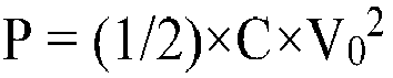
- When a time (maintaining time) in which power consumption can be maintained using the charged energy of the
capacitor 27 is denoted by Th, the following Equation (1) is satisfied. From Equation (1), for example, it can be understood that the maintaining time is shortened by about 20% when the voltage V of the capacitor is reduced by 10% (0. 9×0. 9 = 0. 81).
- In addition, a maximum value Imax of a current flowing through the primary winding 22p is set in advance. For this reason, the flowing equation is satisfied from V0 = P/Imax.

- In a case in which the threshold voltage Vn and the adjustment time T2 are set to Vs and Ts of the previous-time setting values from Equation (1), and a maintaining time Th based on these values is set to a standard maintaining time Ths based on the previous-time setting values, Equation (2) is satisfied.

- Here, Wmax: Maximum rated power of the
power supply unit 100, and Vs: Previous-time setting value of the threshold voltage Vn (the threshold voltage Vn before change). - Then, in a case in which the threshold voltage Vs is changed to the threshold voltage Va, and the maintaining time is set to the maintaining time Tha after change, the following equation is satisfied.

- Here, in addition to the threshold voltage Va, for example, settings of a plurality of stages including Vb, Vc, and Vd and the threshold voltage Vs can be changed.
- An example of the setting will be described with reference to
Fig. 9. Fig. 9 is a diagram illustrating an example of change of a voltage setting of the threshold voltage Vn according to this embodiment. Until now, a configuration in which one switch SW is connected to one resistor R3 in parallel has been described as an example. In contrast to this, a configuration in which switches (switches SWa, SWb, SWc, and SWd) are respectively disposed in a plurality of resistors (resistors R3a, R3b, R3c, and R3d) in parallel will be described with reference to part (A) ofFig. 9 as an example. On/off of such switches, for example, is switched by a user's operation on thechangeover switch 26. - Part (B) of
Fig. 9 illustrates changes in the threshold voltage Vn corresponding to on/off of the switches SWa to SWd. More specifically, in a case in which resistance values of the resistors R3a, Rb, Rc, and R3d are configured to be the same resistance values, when all the switches are off (the switches SWa, SWb, SWc, and SWd are off), a total resistance value of such resistors becomes a maximum. As a result, the threshold voltage becomes a largest threshold voltage (for example, Vs). As the number of switches that are set to on among the switches SWa, SWb, SWc, and SWd becomes larger, the threshold voltage decreases. When all the switches are on (the switches SWa, SWb, SWc, and SWd are on), a total resistance value of such resistors becomes a minimum. As a result, the threshold voltage becomes the threshold voltage Vd and becomes a threshold voltage lower than the other threshold voltages (for example, Va, Vb, and Vc). In addition, thechangeover switch 26, for example, is a rotary switch, and, by switching the switch to one ofnumbers 0 to 9, the threshold voltage Vn can be set to one of a plurality of voltages. For example, the threshold voltage can be changed from a large voltage Vn to a low voltage (Vs > Va > Vb > Vc > Vd). - The values of the threshold voltage Vn and the adjustment time T2 are selected such that a condition represented in Equation (4) is satisfied based on Equation (2) and Equation (3).

- The threshold voltage Vn and the adjustment time T2 are set such that a value acquired by subtracting the maintaining time Tha after change from the maintaining time Ths before change is smaller than a sum of the adjustment time T2 after change (for example, T2a) and the spare time T4. In this way, the threshold voltage Vn and the adjustment time T2 are associated with each other, and, in a case in which the setting of one thereof is changed, the setting of the other needs to be also changed in accordance with details of the change. As a method of changing the setting, for example, as described above, there is a method in which a user sets the threshold voltage Vn using the
changeover switch 26 and changes the adjustment time T2 using thesupport device 300. - Other than those described above, for example, a user may change the threshold voltage Vn and the adjustment time T2 using the
support device 300. In addition, by disposing a switch similar to thechangeover switch 26 also on the surface of theCPU unit 10, a user may change the threshold voltage Vn and the adjustment time T2 by operating thechangeover switch 26 disposed in thepower supply unit 100 and the switch disposed in theCPU unit 10. Furthermore, it may be configured such that a user inputs a value after change of one of the threshold voltage Vn and the adjustment time T2 to thesupport device 300 using the input unit, theCPU 302 calculates a value after change of the other by executing an arithmetic operation process, and the settings of the threshold voltage Vn and the adjustment time T2 are changed based on the value input by the user and the calculated value. - An example of the method of changing the setting will be described with reference to
Fig. 10. Fig. 10 is a diagram illustrating an example of an image displayed in thedisplay 314 in a case in which thesupport device 300 according to this embodiment calculates a threshold voltage Vn. A user inputs a maximum rated output (Wmax) of thepower supply unit 100, maximum power consumption (W0) of theentire PLC system 1, and an adjustment time T2 by operating the input unit of thesupport device 300. TheCPU 302 of thesupport device 300 calculates a threshold voltage Vn by performing an arithmetic operation process based on Equations (2), (3), and (4). The power consumption of theentire PLC system 1 is maximum power that is actually used by theCPU unit 10 and the I/O unit 200. In addition, the maximum rated output of thepower supply unit 100 and the maximum power consumption of theentire PLC system 1 are calculated in advance by thesupport device 300 based on information acquired from thePLC system 1 and is notified to a user. The threshold voltage Vs that is a previous-time setting value in Equation (2) or Equation (3), a maximum value Imax of a current flowing through the primary winding 22p, and the capacitance C of thecapacitor 27 are also calculated in advance by thesupport device 300. TheCPU 302 of thesupport device 300 calculates a threshold voltage Vn (for example, the threshold voltage Va) from the value of the adjustment time T2 (for example, the adjustment time Ta) such that the relationship of Equation (4) is satisfied. The value of the threshold voltage Vn calculated in this way is displayed in thedisplay 314. In this way, thePLC system 1 can display the threshold voltage in thedisplay 314, and a change of the setting of the threshold voltage Vn can be received from a user who has checked the threshold voltage Vn displayed in thedisplay 314. In addition, a user can change the setting of the threshold voltage Vn while checking the threshold voltage Vn displayed in thedisplay 314. - A relation between the adjustment time T2 and the threshold voltage Vn illustrated in
Fig. 10 described above will be described with reference toFig. 11. Fig. 11 illustrates a correspondence relation between the threshold voltage Vn, an amount of charging in thecapacitor 27, and the adjustment time T2 according to this embodiment. In part (A) ofFig. 11 , for example, in a case in which the threshold voltage Vn is set to the largest threshold voltage Vs, the amount of charging in thecapacitor 27 becomes Ps. The adjustment time T2 for the amount of charging Ps becomes the adjustment time T2s. In contrast to this, in part (B) ofFig. 11 , for example, in a case in which the threshold voltage Vn is set to a voltage Va lower than the threshold voltage Vs, the amount of charging in thecapacitor 27 becomes Pa that is Δp smaller than Ps. As a result, the adjustment time T2 becomes Ta that is shorter than the adjustment time Ts. In this way, regarding the threshold voltage Vn, the amount of charging in the capacitor, and the adjustment time T2, when one of the threshold voltage Vn and the adjustment time T2 changes, the other also changes in accordance with the change. In this way, thePLC system 1 can set an optimal threshold voltage Vn based on the set adjustment time T2. In addition, thePLC system 1 can set an optimal adjustment time T2 based on the set threshold voltage Vn. - In addition, in addition to the change of the setting described until now, the
CPU 302 of thesupport device 300 may calculate a threshold voltage Vn (for example, the threshold voltage Va) based on an adjustment time T2 (for example, the adjustment time T2a) input by a user's operation using the input unit. Thesupport device 300 outputs a change instruction signal relating to the input adjustment time T2a to theCPU unit 10 through thecommunication interface 318. Theprocessor 11 of theCPU unit 10 changes the adjustment time T2 of the settinginformation 154 to the adjustment time T2a based on the change instruction signal relating to the received adjustment time T2. In addition, thesupport device 300 outputs a change instruction signal relating to the threshold voltage Va to thepower supply unit 100 through thecommunication interface 318. This change instruction signal may be output from thesupport device 300 to thepower supply unit 100 through theCPU unit 10. Thepower supply unit 100 performs on/off switching of the switch SW based on the change instruction signal relating to the received threshold voltage Vn. In accordance with this, the threshold voltage Vn is changed. In addition, in a case in which a change instruction signal is output through theCPU unit 10, the on/off control of the switch SW may be performed such that, when the change instruction signal is received, theprocessor 11 may read setting information of the threshold voltage Vn from thestorage 150 and execute the process of changing the threshold voltage Vn. The threshold voltage Vn is stored in the settinginformation 154 of thestorage 150 of theCPU unit 10 in advance. In addition, by providing a processor and a storage in thepower supply unit 100, the process may be executed by the processor. - In a case in which the adjustment time T2 is changed to a time that is shorter than a time that has been set at the previous time, the threshold voltage Vn is changed to a voltage lower than a voltage that has been set at the previous time. In addition, in a case in which the adjustment time T2 is changed to a time that is longer than a time that has been set at the previous time, the threshold voltage Vn is changed to a voltage higher than a voltage that has been set at the previous time. In this way, the
PLC system 1 can change the threshold voltage Vn in association with a change in the time T2 of thesecond timer 117, and user convenience at the time of changing the setting is improved. - More specifically, by changing the adjustment time T2 to a time (for example, the adjustment time T2a) shorter than the adjustment time T2s that is the setting value of the previous time, a time in which the
CPU unit 10 can operate after stop of the supply of power becomes shorter than that for the adjustment time T2 before change. However, by changing the threshold voltage Vn to a voltage (for example, the threshold voltage Va) lower than Vs that has been set at the previous time, a frequency at which stop of supply of power is determined decreases. In this way, the operation rate of thePLC system 1 is improved. In a case in which the adjustment time T2 is changed from the adjustment time T2a that has been set at the previous time to another time (for example, the adjustment time T2s) (Ta < Ts), the adjustment time becomes longer than that before change, and thus, a voltage to be charged into the capacitor needs to be a voltage higher than that before change. For this reason, in a case in which the threshold voltage that has been set at the previous time is Va, the threshold voltage Vn is changed to a voltage higher than that (for example, the threshold voltage Vs). In this way, the adjustment time T2 and the threshold voltage Vn of thePLC system 1 are changed in association with each other. In this way, thePLC system 1 can adjust a frequency at which stop of the supply of power is determined in accordance with the form of the system, and a necessary process after the determination of stop of the supply of power can be reliably executed. - In addition, the
CPU 302 of thesupport device 300 may calculate an adjustment time T2 (for example, the adjustment time T2a) based on a threshold voltage (for example, the threshold voltage Va) input from the input unit by a user. Thesupport device 300 outputs a change instruction signal relating to the input threshold voltage Va to thepower supply unit 100 through thecommunication interface 318. This change instruction signal may be output from thesupport device 300 to thepower supply unit 100 through theCPU unit 10. Thepower supply unit 100 performs on/off switching of the switch SW based on the change instruction signal relating to the received threshold voltage Vn, whereby the threshold voltage Vn is changed. In addition, in a case in which a change instruction signal is output through theCPU unit 10, similar to the description presented above, on/off control of the switch SW may be performed such that, when the change instruction signal is received, theprocessor 11 reads setting information of the threshold voltage Vn from thestorage 150 and execute the process of changing the threshold voltage Vn. The threshold voltage Vn is stored in the settinginformation 154 of thestorage 150 theCPU unit 10 in advance. In addition, a processor and a storage may be provided in thepower supply unit 100, and the process may be executed by the processor. Thesupport device 300 outputs the change instruction signal relating to the adjustment time T2a to theCPU unit 10 through thecommunication interface 318. Theprocessor 11 of theCPU unit 10 changes the adjustment time T2 of the settinginformation 154 to the adjustment time T2a based on received the change instruction signal relating to the adjustment time T2. - Then, in a case in which the threshold voltage Vn is changed to a voltage lower than the voltage that has been set at the previous time, the adjustment time T2 is changed to a time shorter than that set at the previous time. In addition, in a case in which the threshold voltage Vn is changed to a voltage higher than the voltage that has been set at the previous time, the adjustment time T2 is changed to a time longer than that set at the previous time. In this way, the
PLC system 1 can change the time T2 of thesecond timer 117 in association with a change of the threshold voltage Vn, and user's convenience at the time of performing a setting change is improved. - More specifically, by changing the threshold voltage Vn to a voltage (for example, the threshold voltage Va) lower than the setting value Vs of the previous time, a voltage charged into the
capacitor 27 becomes lower than that at the time of the setting value Vs of the previous time. The operation time of theCPU unit 10 in a case in which the supply of power stops is shortened than that before the change of the threshold voltage Vn. For this reason, the adjustment time T2 is changed to a time (for example, the adjustment time T2a) that is shorter than the setting value T2s of the previous time. In a case in which the threshold voltage Vn is changed from Va that has been set at the previous time to another value (for example, the threshold voltage Vs) (Va < Vs), the voltage charged into thecapacitor 27 becomes higher than that before the change. The operation time of theCPU unit 10 in a case in which the supply of power stops becomes longer than that before the change of the threshold voltage Vn. The adjustment time T2 is changed to a time (for example, the adjustment time T2s) that is longer than the adjustment time T2a that has been set at the previous time. In this way, the threshold voltage Vn and the adjustment time T2 of thePLC system 1 are changed in association with each other. In this way, thePLC system 1 can adjust a frequency at which the supply of power is determined to have stopped in accordance with the form of the system, and a necessary process after the determination of stop of the supply of power can be reliably executed. - In this embodiment, for example, in
Fig. 5 , while an example of the configuration in which necessary functions are provided by theprocessor 11 executing programs is illustrated, some or all of such provided functions may be implemented using a dedicated hardware circuit (for example, an ASIC, an FPGA, or the like). Alternatively, a main part of theCPU unit 10 may be realized using hardware (for example, an industrial PC based on a general computer) following a general architecture. In such a case, by using a virtualization technology, a plurality of operating systems (OS) having different purposes may be executed in parallel, and a necessary application may be executed on each OS. In this embodiment, in thePLC system 1 illustrated inFig. 5 , although theCPU unit 10 and thesupport device 300 are configured as separate bodies, a configuration in which all or some of functions of those are integrated in a single device may be employed. - In this embodiment, for example, although detection timings of the instantaneous stop detection signal SN1, the power interruption detection signal SN2, and the power supply detection signal SN3 illustrated in
Figs. 6 and7 and a CPU reset signal RS are set as switching timings from a low signal -> a high signal, switching timings from a high signal -> a low signal may be used. - In this embodiment, for example, the timing diagrams illustrated in
Figs. 6 and7 are displayed on thedisplay 314 of thesupport device 300, and a user may set the threshold voltage Vn and the adjustment time T2 by operating thechangeover switch 26 while checking transitions of parameters such as the AC input voltage and the like in a time series. - An embodiment of the present disclosure includes disclosures as below.
- A control system (1) including: a calculation unit (10) configured to execute an arithmetic operation process; and a power supply unit (100) configured to supply power to the calculation unit (10), the power supply unit (100) includes: a power converting unit (201) configured to use a part of an input power input from the outside for charging and convert a remainder of the input power into power supplied to the calculation unit (10); and a first detection unit (127) configured to compare a voltage of the input power with a threshold voltage and output a notification signal for notifying that predetermined power supply is not able to be performed in a case in which a time, over which a magnitude of the voltage has been lower than the threshold voltage, is detected to be over a first measurement time set in advance, the first detection unit (127) being configured to be able to change a setting of the threshold voltage by an external operation, and the calculation unit (10) includes: a second detection unit (117) configured to output an instruction signal for an instruction for execution of pre-stop processing in preparation for stopping of the predetermined power supply in a case in which it is detected that a second measurement time set in advance has elapsed after receiving the notification signal; and a processing execution management unit (111) configured to continue execution of the arithmetic operation process during the second measurement time and execute the pre-stop processing in place of the arithmetic operation process that is currently being executed after receiving the instruction signal, the second detection unit (117) being configured to be able to change a setting of the second measurement time by an external operation.
- The control system described in
Configuration 1, further including a third detection unit (118) configured to output a stop instruction signal in a case in which a third measurement time for ending the arithmetic operation process using the calculation unit (10) has elapsed. - The control system described in
Configuration 1 or 2, a switch that is able to change the setting of the threshold voltage by the external operation is disposed on a surface of the power supply unit (100). - The control system described in one of
Configurations 1 to 3, in the first detection unit (127), the threshold voltage is changed to a voltage lower than a voltage that has been set at a previous time in a case in which the second measurement time is changed to a time shorter than a time that has been set at a previous time, and the threshold voltage is changed to a voltage higher than a voltage that has been set at the previous time in a case in which the second measurement time is changed to a time longer than a time that has been set at the previous time. - The control system described in any one of
Configurations 1 to 3, in the second detection unit (117), the second measurement time is changed to a time shorter than a time that has been set at the previous time in a case in which the threshold voltage is changed to a voltage lower than a voltage that has been set at a previous time, and the second measurement time is changed to a time longer than a time that has been set at a previous time in a case in which the threshold voltage is changed to a voltage higher than a voltage that has been set at the previous time. - The control system according to any one of
Configurations 1 to 5, further including a support device (300) configured to be electrically connected to the calculation unit (10), and the support device (300) includes: a calculation part (302) configured to calculate the threshold voltage corresponding to the second measurement time; and a display part (314) configured to display information relating to the threshold voltage. - A power supply unit (100) that supplies power to a calculation unit (10) executing an arithmetic operation process, the power supply unit including: a power converting unit (201) configured to use a part of an input power input from the outside for charging and convert a remainder of the input power into power supplied to the calculation unit (10); and a first detection unit (127) configured to compare a voltage of the input power with a threshold voltage and output a notification signal for notifying that predetermined power supply is not able to be performed in a case in which a time, over which a magnitude of the voltage has been lower than the threshold voltage, is detected to be over a first measurement time set in advance, the calculation unit (10) is configured to receive the notification signal from the first detection unit (100), issue an execution signal for executing pre-stop processing in preparation for stopping of the predetermined power supply when a second measurement time set in advance has elapsed, continue to execute the arithmetic operation process during the second measurement time, execute the pre-stop processing in place of the arithmetic operation process that is currently being executed after the execution signal is received, and be able to change the setting of the second measurement time by an external operation, and the first detection unit (127) is configured to be able to change the setting of the threshold voltage by an external operation.
- The embodiment disclosed here is an example in every aspect and should be considered as not being limited. The scope of the present disclosure is represented not by the description presented above but by claims, and all the changes made within the meaning and the range equivalent to the claims are intended to be included therein.
-
- 1 control system
- 10A input unit
- 11 processor
- 20B power supply unit
- 21 rectification circuit
- 22 transformer
- 22a auxiliary winding
- 22p primary winding
- 22s secondary winding
- 23 MOSFET
- 24 rectification smoothing circuit
- 25 noise filter
- 26 changeover switch
- 27, 45, 46 capacitor
- 28 drive control circuit
- 29 overcurrent detecting circuit
- 30C output unit
- 40 amplitude detecting circuit
- 41 voltage detecting circuit
- 42 instantaneous stop detecting circuit
- 43, 44 photo coupler
- 52 memory card interface
- 55 fuse
- 100 power supply unit
- 111 scheduler
- 117 second timer
- 118 third timer
- 120 power supply circuit
- 127 first timer
- 130 chip set
- 150 storage
- 151 user program
- 152 sequence program
- 153 system program
- 154 setting information
- 161 main memory
- 162 internal bus controller
- 163 high-rank network controller
- 165 field network controller
- 172 field device
- 178 memory card
- 180 USB controller
- 190 memory card controller
- 201 power converting unit
- 202 system bus
- 211 DC/DC converter
- 300 support device
- 306 RAM
- 310 keyboard
- 312 mouse
- 314 display
- 317 recording media reading device
- 318 communication interface
- 350 recording medium
- 401 Zener diode
- 402 operational amplifier
- 403 transistor
- 421 comparator
Claims (7)
- A control system comprising:a calculation unit that executes an arithmetic operation process; anda power supply unit that supplies power to the calculation unit,wherein the power supply unit includes:a power converting unit that charges a part of an input power input from an outside and converts a remainder of the input power into the power supplied to the calculation unit; anda first detection unit that compares a voltage of the input power with a threshold voltage and outputs a notification signal for notifying that predetermined power supply is not able to be performed in a case in which a time, over which a magnitude of the voltage has been lower than the threshold voltage, is detected to be over a first measurement time set in advance,the first detection unit is able to change a setting of the threshold voltage by an external operation, andwherein the calculation unit includes:a second detection unit that outputs an instruction signal for instructing an execution of pre-stop processing in preparation for stopping of the predetermined power supply in a case in which it is detected that a second measurement time set in advance has elapsed after receiving the notification signal; anda processing execution management unit that continues execution of the arithmetic operation process during the second measurement time and executes the pre-stop processing in place of the arithmetic operation process that is currently being executed after receiving the instruction signal,the second detection unit is able to change a setting of the second measurement time by an external operation.
- The control system according to claim 1, further comprising a third detection unit that outputs a stop instruction signal in a case in which a third measurement time for ending the arithmetic operation process made by the calculation unit has elapsed.
- The control system according to claim 1 or 2, wherein a switch that is able to change the setting of the threshold voltage by the external operation is disposed on a surface of the power supply unit.
- The control system according to any one of claims 1 to3, wherein, in the first detection unit, the threshold voltage is changed to a voltage lower than a voltage that has been set at a previous time in a case in which the second measurement time is changed to a time shorter than a time that has been set at the previous time, and the threshold voltage is changed to a voltage higher than a voltage that has been set at a previous time in a case in which the second measurement time is changed to a time longer than a time that has been set at the previous time.
- The control system according to any one of claims 1 to 3, wherein, in the second detection unit, the second measurement time is changed to a time shorter than a time that has been set at a previous time in a case in which the threshold voltage is changed to a voltage lower than a voltage that has been set at the previous time, and the second measurement time is changed to a time longer than a time that has been set at a previous time in a case in which the threshold voltage is changed to a voltage higher than a voltage that has been set at the previous time.
- The control system according to any one of claims 1 to 5, further comprising a support device that is electrically connected to the calculation unit,
wherein the support device includes:a calculation part that calculates the threshold voltage corresponding to the second measurement time; anda display part that displays information relating to the threshold voltage. - A power supply unit that supplies power to a calculation unit executing an arithmetic operation process, the power supply unit comprising:a power converting unit that charges a part of an input power input from an outside and converts a remainder of the input power into power supplied to the calculation unit; anda first detection unit that compares a voltage of the input power with a threshold voltage and outputs a notification signal for notifying that predetermined power supply is not able to be performed in a case in which a time, over which a magnitude of the voltage has been lower than the threshold voltage, is detected to be over a first measurement time set in advance,wherein the calculation unit receives the notification signal from the first detection unit, issues an execution signal for executing pre-stop processing in preparation for stopping of the predetermined power supply when a second measurement time set in advance has elapsed, continues to execute the arithmetic operation process during the second measurement time, executes the pre-stop processing in place of the arithmetic operation process that is currently being executed after the execution signal is received, and is able to change the setting of the second measurement time by an external operation, andwherein the first detection unit is able to change a setting of the threshold voltage by an external operation.
Applications Claiming Priority (2)
| Application Number | Priority Date | Filing Date | Title |
|---|---|---|---|
| JP2018096951A JP7000989B2 (en) | 2018-05-21 | 2018-05-21 | Control system |
| PCT/JP2019/016990 WO2019225253A1 (en) | 2018-05-21 | 2019-04-22 | Control system and power supply unit |
Publications (3)
| Publication Number | Publication Date |
|---|---|
| EP3799286A1 true EP3799286A1 (en) | 2021-03-31 |
| EP3799286A4 EP3799286A4 (en) | 2022-03-16 |
| EP3799286B1 EP3799286B1 (en) | 2024-01-03 |
Family
ID=68615627
Family Applications (1)
| Application Number | Title | Priority Date | Filing Date |
|---|---|---|---|
| EP19807575.6A Active EP3799286B1 (en) | 2018-05-21 | 2019-04-22 | Control system and power supply unit |
Country Status (5)
| Country | Link |
|---|---|
| US (1) | US11368094B2 (en) |
| EP (1) | EP3799286B1 (en) |
| JP (1) | JP7000989B2 (en) |
| CN (1) | CN111971887B (en) |
| WO (1) | WO2019225253A1 (en) |
Families Citing this family (3)
| Publication number | Priority date | Publication date | Assignee | Title |
|---|---|---|---|---|
| WO2021149634A1 (en) * | 2020-01-20 | 2021-07-29 | ファナック株式会社 | Control device of robot and power outage processing method |
| US11493980B1 (en) | 2021-05-17 | 2022-11-08 | Qualcomm Incorporated | Power controller communication latency mitigation |
| CN117651941B (en) * | 2021-09-10 | 2024-10-22 | 三菱电机株式会社 | Controller unit and power supply operation method of general operating system |
Family Cites Families (15)
| Publication number | Priority date | Publication date | Assignee | Title |
|---|---|---|---|---|
| JP3664692B2 (en) * | 2002-04-22 | 2005-06-29 | 三菱電機株式会社 | Arithmetic processing unit |
| JP4246031B2 (en) * | 2003-10-22 | 2009-04-02 | シャープ株式会社 | Electronics |
| WO2005088819A1 (en) | 2004-03-17 | 2005-09-22 | Matsushita Electric Industrial Co., Ltd. | Switching power supply device |
| JP5039322B2 (en) * | 2006-05-09 | 2012-10-03 | ローム株式会社 | Start-up circuit, method, and low-voltage malfunction prevention circuit, power supply circuit, and electronic device using the same |
| JP4235919B2 (en) | 2006-10-06 | 2009-03-11 | コニカミノルタビジネステクノロジーズ株式会社 | Information processing apparatus and program |
| JP5177148B2 (en) * | 2007-12-25 | 2013-04-03 | 株式会社村田製作所 | Processor and switching power supply |
| CN102033502B (en) * | 2009-09-25 | 2014-04-02 | 松下神视株式会社 | Programmable controller |
| JP5979955B2 (en) * | 2012-04-20 | 2016-08-31 | ルネサスエレクトロニクス株式会社 | Semiconductor integrated circuit device, power supply device, and control method of power supply device |
| JP5820779B2 (en) * | 2012-07-06 | 2015-11-24 | 日立オートモティブシステムズ株式会社 | In-vehicle power supply |
| JP6214924B2 (en) * | 2012-09-14 | 2017-10-18 | ルネサスエレクトロニクス株式会社 | Controller and system having controller |
| JP2014090624A (en) * | 2012-10-31 | 2014-05-15 | Sanken Electric Co Ltd | Ac input voltage detection circuit and ac/dc power supply |
| US9494658B2 (en) * | 2013-03-14 | 2016-11-15 | Flextronics Ap, Llc | Approach for generation of power failure warning signal to maximize useable hold-up time with AC/DC rectifiers |
| JP6213117B2 (en) * | 2013-10-04 | 2017-10-18 | コニカミノルタ株式会社 | Control device and image forming apparatus |
| CN104731723A (en) * | 2015-03-19 | 2015-06-24 | 青岛海信电器股份有限公司 | Power-off protection method and device for storage device |
| JP6812736B2 (en) * | 2016-10-07 | 2021-01-13 | オムロン株式会社 | Arithmetic logic unit and control unit |
-
2018
- 2018-05-21 JP JP2018096951A patent/JP7000989B2/en active Active
-
2019
- 2019-04-22 WO PCT/JP2019/016990 patent/WO2019225253A1/en not_active Ceased
- 2019-04-22 EP EP19807575.6A patent/EP3799286B1/en active Active
- 2019-04-22 US US17/043,718 patent/US11368094B2/en active Active
- 2019-04-22 CN CN201980025742.0A patent/CN111971887B/en active Active
Also Published As
| Publication number | Publication date |
|---|---|
| CN111971887A (en) | 2020-11-20 |
| EP3799286B1 (en) | 2024-01-03 |
| WO2019225253A1 (en) | 2019-11-28 |
| JP2019205228A (en) | 2019-11-28 |
| US11368094B2 (en) | 2022-06-21 |
| US20210028707A1 (en) | 2021-01-28 |
| JP7000989B2 (en) | 2022-01-19 |
| EP3799286A4 (en) | 2022-03-16 |
| CN111971887B (en) | 2023-09-26 |
Similar Documents
| Publication | Publication Date | Title |
|---|---|---|
| US8675891B2 (en) | Power supply unit with noise reduction capability | |
| US8193794B2 (en) | Voltage regulator having an output voltage automatically adjusted according to a load current | |
| JP5160033B2 (en) | Methods, systems, and adjustment techniques for power measurement and power saving for multiple time frames | |
| US8330442B2 (en) | DC to DC converter and method for reducing overshoot | |
| EP3799286B1 (en) | Control system and power supply unit | |
| US7688047B2 (en) | Power circuit and method of rising output voltage of power circuit | |
| EP3346596A1 (en) | Symmetric time shift control for resonant converters | |
| EP2701297B1 (en) | Electronic apparatus and power controlling method thereof | |
| JP2000014043A (en) | Uninterruptive power supply | |
| JP2014082919A (en) | Controller and system having controller | |
| JP2017531986A (en) | Integrated circuit with external resistance detection | |
| CN101242137A (en) | Power-on reset circuit and method for generating power-on reset signal | |
| US8022672B2 (en) | Charger control circuit and charger control method | |
| US10718798B2 (en) | AC voltage detection device, image forming apparatus, and industrial machine | |
| US20160087519A1 (en) | Switching Power-Supply Device | |
| US9559599B2 (en) | Electronic apparatus for generating a pulse width modulation and power controlling method thereof | |
| US12455603B2 (en) | Universal serial bus power delivery (USB-PD) | |
| JP2003169476A (en) | Electronic equipment to which a power supply adapter can be connected | |
| US7368895B2 (en) | Apparatus for a power supply with brownout protection and the protecting method for the same | |
| CN116247919A (en) | Method for switching operation modes of power converters | |
| US8742730B2 (en) | Charging circuit | |
| JP2016142632A (en) | Power measurement device and current measurement device | |
| KR20210137837A (en) | Method and apparatus for estimating a lifetime of DC-link capacitors in a power conversion device | |
| CN121036497A (en) | Hybrid modulation methods, systems, devices and media for isolated power supply chips | |
| JP2002091605A (en) | Power consumption reducing circuit |
Legal Events
| Date | Code | Title | Description |
|---|---|---|---|
| STAA | Information on the status of an ep patent application or granted ep patent |
Free format text: STATUS: THE INTERNATIONAL PUBLICATION HAS BEEN MADE |
|
| PUAI | Public reference made under article 153(3) epc to a published international application that has entered the european phase |
Free format text: ORIGINAL CODE: 0009012 |
|
| STAA | Information on the status of an ep patent application or granted ep patent |
Free format text: STATUS: REQUEST FOR EXAMINATION WAS MADE |
|
| 17P | Request for examination filed |
Effective date: 20201109 |
|
| AK | Designated contracting states |
Kind code of ref document: A1 Designated state(s): AL AT BE BG CH CY CZ DE DK EE ES FI FR GB GR HR HU IE IS IT LI LT LU LV MC MK MT NL NO PL PT RO RS SE SI SK SM TR |
|
| AX | Request for extension of the european patent |
Extension state: BA ME |
|
| DAV | Request for validation of the european patent (deleted) | ||
| DAX | Request for extension of the european patent (deleted) | ||
| REG | Reference to a national code |
Ref country code: DE Ref legal event code: R079 Free format text: PREVIOUS MAIN CLASS: H02M0003280000 Ipc: G06F0001300000 Ref country code: DE Ref legal event code: R079 Ref document number: 602019044546 Country of ref document: DE Free format text: PREVIOUS MAIN CLASS: H02M0003280000 Ipc: G06F0001300000 |
|
| A4 | Supplementary search report drawn up and despatched |
Effective date: 20220210 |
|
| RIC1 | Information provided on ipc code assigned before grant |
Ipc: H02M 1/36 20070101ALI20220204BHEP Ipc: H03K 5/24 20060101ALI20220204BHEP Ipc: H02M 3/335 20060101ALI20220204BHEP Ipc: G05B 19/05 20060101ALI20220204BHEP Ipc: H05K 7/14 20060101ALI20220204BHEP Ipc: H02M 3/28 20060101ALI20220204BHEP Ipc: G06F 1/28 20060101ALI20220204BHEP Ipc: G06F 1/30 20060101AFI20220204BHEP |
|
| GRAP | Despatch of communication of intention to grant a patent |
Free format text: ORIGINAL CODE: EPIDOSNIGR1 |
|
| STAA | Information on the status of an ep patent application or granted ep patent |
Free format text: STATUS: GRANT OF PATENT IS INTENDED |
|
| INTG | Intention to grant announced |
Effective date: 20230728 |
|
| GRAS | Grant fee paid |
Free format text: ORIGINAL CODE: EPIDOSNIGR3 |
|
| GRAA | (expected) grant |
Free format text: ORIGINAL CODE: 0009210 |
|
| STAA | Information on the status of an ep patent application or granted ep patent |
Free format text: STATUS: THE PATENT HAS BEEN GRANTED |
|
| AK | Designated contracting states |
Kind code of ref document: B1 Designated state(s): AL AT BE BG CH CY CZ DE DK EE ES FI FR GB GR HR HU IE IS IT LI LT LU LV MC MK MT NL NO PL PT RO RS SE SI SK SM TR |
|
| REG | Reference to a national code |
Ref country code: GB Ref legal event code: FG4D |
|
| REG | Reference to a national code |
Ref country code: DE Ref legal event code: R096 Ref document number: 602019044546 Country of ref document: DE |
|
| REG | Reference to a national code |
Ref country code: CH Ref legal event code: EP |
|
| REG | Reference to a national code |
Ref country code: IE Ref legal event code: FG4D |
|
| REG | Reference to a national code |
Ref country code: LT Ref legal event code: MG9D |
|
| PG25 | Lapsed in a contracting state [announced via postgrant information from national office to epo] |
Ref country code: ES Free format text: LAPSE BECAUSE OF FAILURE TO SUBMIT A TRANSLATION OF THE DESCRIPTION OR TO PAY THE FEE WITHIN THE PRESCRIBED TIME-LIMIT Effective date: 20240103 |
|
| PG25 | Lapsed in a contracting state [announced via postgrant information from national office to epo] |
Ref country code: ES Free format text: LAPSE BECAUSE OF FAILURE TO SUBMIT A TRANSLATION OF THE DESCRIPTION OR TO PAY THE FEE WITHIN THE PRESCRIBED TIME-LIMIT Effective date: 20240103 |
|
| REG | Reference to a national code |
Ref country code: NL Ref legal event code: MP Effective date: 20240103 |
|
| REG | Reference to a national code |
Ref country code: AT Ref legal event code: MK05 Ref document number: 1647465 Country of ref document: AT Kind code of ref document: T Effective date: 20240103 |
|
| PG25 | Lapsed in a contracting state [announced via postgrant information from national office to epo] |
Ref country code: NL Free format text: LAPSE BECAUSE OF FAILURE TO SUBMIT A TRANSLATION OF THE DESCRIPTION OR TO PAY THE FEE WITHIN THE PRESCRIBED TIME-LIMIT Effective date: 20240103 |
|
| PG25 | Lapsed in a contracting state [announced via postgrant information from national office to epo] |
Ref country code: NL Free format text: LAPSE BECAUSE OF FAILURE TO SUBMIT A TRANSLATION OF THE DESCRIPTION OR TO PAY THE FEE WITHIN THE PRESCRIBED TIME-LIMIT Effective date: 20240103 |
|
| PG25 | Lapsed in a contracting state [announced via postgrant information from national office to epo] |
Ref country code: IS Free format text: LAPSE BECAUSE OF FAILURE TO SUBMIT A TRANSLATION OF THE DESCRIPTION OR TO PAY THE FEE WITHIN THE PRESCRIBED TIME-LIMIT Effective date: 20240503 |
|
| PG25 | Lapsed in a contracting state [announced via postgrant information from national office to epo] |
Ref country code: LT Free format text: LAPSE BECAUSE OF FAILURE TO SUBMIT A TRANSLATION OF THE DESCRIPTION OR TO PAY THE FEE WITHIN THE PRESCRIBED TIME-LIMIT Effective date: 20240103 |
|
| PG25 | Lapsed in a contracting state [announced via postgrant information from national office to epo] |
Ref country code: GR Free format text: LAPSE BECAUSE OF FAILURE TO SUBMIT A TRANSLATION OF THE DESCRIPTION OR TO PAY THE FEE WITHIN THE PRESCRIBED TIME-LIMIT Effective date: 20240404 |
|
| PG25 | Lapsed in a contracting state [announced via postgrant information from national office to epo] |
Ref country code: RS Free format text: LAPSE BECAUSE OF FAILURE TO SUBMIT A TRANSLATION OF THE DESCRIPTION OR TO PAY THE FEE WITHIN THE PRESCRIBED TIME-LIMIT Effective date: 20240403 Ref country code: HR Free format text: LAPSE BECAUSE OF FAILURE TO SUBMIT A TRANSLATION OF THE DESCRIPTION OR TO PAY THE FEE WITHIN THE PRESCRIBED TIME-LIMIT Effective date: 20240103 |
|
| PG25 | Lapsed in a contracting state [announced via postgrant information from national office to epo] |
Ref country code: CZ Free format text: LAPSE BECAUSE OF FAILURE TO SUBMIT A TRANSLATION OF THE DESCRIPTION OR TO PAY THE FEE WITHIN THE PRESCRIBED TIME-LIMIT Effective date: 20240103 Ref country code: AT Free format text: LAPSE BECAUSE OF FAILURE TO SUBMIT A TRANSLATION OF THE DESCRIPTION OR TO PAY THE FEE WITHIN THE PRESCRIBED TIME-LIMIT Effective date: 20240103 |
|
| PG25 | Lapsed in a contracting state [announced via postgrant information from national office to epo] |
Ref country code: RS Free format text: LAPSE BECAUSE OF FAILURE TO SUBMIT A TRANSLATION OF THE DESCRIPTION OR TO PAY THE FEE WITHIN THE PRESCRIBED TIME-LIMIT Effective date: 20240403 Ref country code: NO Free format text: LAPSE BECAUSE OF FAILURE TO SUBMIT A TRANSLATION OF THE DESCRIPTION OR TO PAY THE FEE WITHIN THE PRESCRIBED TIME-LIMIT Effective date: 20240403 Ref country code: LT Free format text: LAPSE BECAUSE OF FAILURE TO SUBMIT A TRANSLATION OF THE DESCRIPTION OR TO PAY THE FEE WITHIN THE PRESCRIBED TIME-LIMIT Effective date: 20240103 Ref country code: IS Free format text: LAPSE BECAUSE OF FAILURE TO SUBMIT A TRANSLATION OF THE DESCRIPTION OR TO PAY THE FEE WITHIN THE PRESCRIBED TIME-LIMIT Effective date: 20240503 Ref country code: HR Free format text: LAPSE BECAUSE OF FAILURE TO SUBMIT A TRANSLATION OF THE DESCRIPTION OR TO PAY THE FEE WITHIN THE PRESCRIBED TIME-LIMIT Effective date: 20240103 Ref country code: GR Free format text: LAPSE BECAUSE OF FAILURE TO SUBMIT A TRANSLATION OF THE DESCRIPTION OR TO PAY THE FEE WITHIN THE PRESCRIBED TIME-LIMIT Effective date: 20240404 Ref country code: CZ Free format text: LAPSE BECAUSE OF FAILURE TO SUBMIT A TRANSLATION OF THE DESCRIPTION OR TO PAY THE FEE WITHIN THE PRESCRIBED TIME-LIMIT Effective date: 20240103 Ref country code: BG Free format text: LAPSE BECAUSE OF FAILURE TO SUBMIT A TRANSLATION OF THE DESCRIPTION OR TO PAY THE FEE WITHIN THE PRESCRIBED TIME-LIMIT Effective date: 20240103 Ref country code: AT Free format text: LAPSE BECAUSE OF FAILURE TO SUBMIT A TRANSLATION OF THE DESCRIPTION OR TO PAY THE FEE WITHIN THE PRESCRIBED TIME-LIMIT Effective date: 20240103 |
|
| PG25 | Lapsed in a contracting state [announced via postgrant information from national office to epo] |
Ref country code: PL Free format text: LAPSE BECAUSE OF FAILURE TO SUBMIT A TRANSLATION OF THE DESCRIPTION OR TO PAY THE FEE WITHIN THE PRESCRIBED TIME-LIMIT Effective date: 20240103 Ref country code: PT Free format text: LAPSE BECAUSE OF FAILURE TO SUBMIT A TRANSLATION OF THE DESCRIPTION OR TO PAY THE FEE WITHIN THE PRESCRIBED TIME-LIMIT Effective date: 20240503 |
|
| PG25 | Lapsed in a contracting state [announced via postgrant information from national office to epo] |
Ref country code: SE Free format text: LAPSE BECAUSE OF FAILURE TO SUBMIT A TRANSLATION OF THE DESCRIPTION OR TO PAY THE FEE WITHIN THE PRESCRIBED TIME-LIMIT Effective date: 20240103 Ref country code: PT Free format text: LAPSE BECAUSE OF FAILURE TO SUBMIT A TRANSLATION OF THE DESCRIPTION OR TO PAY THE FEE WITHIN THE PRESCRIBED TIME-LIMIT Effective date: 20240503 Ref country code: PL Free format text: LAPSE BECAUSE OF FAILURE TO SUBMIT A TRANSLATION OF THE DESCRIPTION OR TO PAY THE FEE WITHIN THE PRESCRIBED TIME-LIMIT Effective date: 20240103 Ref country code: LV Free format text: LAPSE BECAUSE OF FAILURE TO SUBMIT A TRANSLATION OF THE DESCRIPTION OR TO PAY THE FEE WITHIN THE PRESCRIBED TIME-LIMIT Effective date: 20240103 |
|
| REG | Reference to a national code |
Ref country code: DE Ref legal event code: R097 Ref document number: 602019044546 Country of ref document: DE |
|
| PG25 | Lapsed in a contracting state [announced via postgrant information from national office to epo] |
Ref country code: DK Free format text: LAPSE BECAUSE OF FAILURE TO SUBMIT A TRANSLATION OF THE DESCRIPTION OR TO PAY THE FEE WITHIN THE PRESCRIBED TIME-LIMIT Effective date: 20240103 |
|
| PG25 | Lapsed in a contracting state [announced via postgrant information from national office to epo] |
Ref country code: SM Free format text: LAPSE BECAUSE OF FAILURE TO SUBMIT A TRANSLATION OF THE DESCRIPTION OR TO PAY THE FEE WITHIN THE PRESCRIBED TIME-LIMIT Effective date: 20240103 |
|
| PG25 | Lapsed in a contracting state [announced via postgrant information from national office to epo] |
Ref country code: EE Free format text: LAPSE BECAUSE OF FAILURE TO SUBMIT A TRANSLATION OF THE DESCRIPTION OR TO PAY THE FEE WITHIN THE PRESCRIBED TIME-LIMIT Effective date: 20240103 |
|
| PG25 | Lapsed in a contracting state [announced via postgrant information from national office to epo] |
Ref country code: SK Free format text: LAPSE BECAUSE OF FAILURE TO SUBMIT A TRANSLATION OF THE DESCRIPTION OR TO PAY THE FEE WITHIN THE PRESCRIBED TIME-LIMIT Effective date: 20240103 |
|
| PG25 | Lapsed in a contracting state [announced via postgrant information from national office to epo] |
Ref country code: SM Free format text: LAPSE BECAUSE OF FAILURE TO SUBMIT A TRANSLATION OF THE DESCRIPTION OR TO PAY THE FEE WITHIN THE PRESCRIBED TIME-LIMIT Effective date: 20240103 Ref country code: SK Free format text: LAPSE BECAUSE OF FAILURE TO SUBMIT A TRANSLATION OF THE DESCRIPTION OR TO PAY THE FEE WITHIN THE PRESCRIBED TIME-LIMIT Effective date: 20240103 Ref country code: RO Free format text: LAPSE BECAUSE OF FAILURE TO SUBMIT A TRANSLATION OF THE DESCRIPTION OR TO PAY THE FEE WITHIN THE PRESCRIBED TIME-LIMIT Effective date: 20240103 Ref country code: EE Free format text: LAPSE BECAUSE OF FAILURE TO SUBMIT A TRANSLATION OF THE DESCRIPTION OR TO PAY THE FEE WITHIN THE PRESCRIBED TIME-LIMIT Effective date: 20240103 Ref country code: DK Free format text: LAPSE BECAUSE OF FAILURE TO SUBMIT A TRANSLATION OF THE DESCRIPTION OR TO PAY THE FEE WITHIN THE PRESCRIBED TIME-LIMIT Effective date: 20240103 |
|
| PLBE | No opposition filed within time limit |
Free format text: ORIGINAL CODE: 0009261 |
|
| STAA | Information on the status of an ep patent application or granted ep patent |
Free format text: STATUS: NO OPPOSITION FILED WITHIN TIME LIMIT |
|
| PG25 | Lapsed in a contracting state [announced via postgrant information from national office to epo] |
Ref country code: MC Free format text: LAPSE BECAUSE OF FAILURE TO SUBMIT A TRANSLATION OF THE DESCRIPTION OR TO PAY THE FEE WITHIN THE PRESCRIBED TIME-LIMIT Effective date: 20240103 |
|
| PG25 | Lapsed in a contracting state [announced via postgrant information from national office to epo] |
Ref country code: MC Free format text: LAPSE BECAUSE OF FAILURE TO SUBMIT A TRANSLATION OF THE DESCRIPTION OR TO PAY THE FEE WITHIN THE PRESCRIBED TIME-LIMIT Effective date: 20240103 |
|
| REG | Reference to a national code |
Ref country code: CH Ref legal event code: PL |
|
| PG25 | Lapsed in a contracting state [announced via postgrant information from national office to epo] |
Ref country code: IT Free format text: LAPSE BECAUSE OF FAILURE TO SUBMIT A TRANSLATION OF THE DESCRIPTION OR TO PAY THE FEE WITHIN THE PRESCRIBED TIME-LIMIT Effective date: 20240103 |
|
| 26N | No opposition filed |
Effective date: 20241007 |
|
| PG25 | Lapsed in a contracting state [announced via postgrant information from national office to epo] |
Ref country code: LU Free format text: LAPSE BECAUSE OF NON-PAYMENT OF DUE FEES Effective date: 20240422 |
|
| GBPC | Gb: european patent ceased through non-payment of renewal fee |
Effective date: 20240422 |
|
| REG | Reference to a national code |
Ref country code: BE Ref legal event code: MM Effective date: 20240430 |
|
| PG25 | Lapsed in a contracting state [announced via postgrant information from national office to epo] |
Ref country code: LU Free format text: LAPSE BECAUSE OF NON-PAYMENT OF DUE FEES Effective date: 20240422 Ref country code: IT Free format text: LAPSE BECAUSE OF FAILURE TO SUBMIT A TRANSLATION OF THE DESCRIPTION OR TO PAY THE FEE WITHIN THE PRESCRIBED TIME-LIMIT Effective date: 20240103 |
|
| PG25 | Lapsed in a contracting state [announced via postgrant information from national office to epo] |
Ref country code: BE Free format text: LAPSE BECAUSE OF NON-PAYMENT OF DUE FEES Effective date: 20240430 |
|
| PG25 | Lapsed in a contracting state [announced via postgrant information from national office to epo] |
Ref country code: GB Free format text: LAPSE BECAUSE OF NON-PAYMENT OF DUE FEES Effective date: 20240422 |
|
| PG25 | Lapsed in a contracting state [announced via postgrant information from national office to epo] |
Ref country code: FR Free format text: LAPSE BECAUSE OF NON-PAYMENT OF DUE FEES Effective date: 20240430 |
|
| PG25 | Lapsed in a contracting state [announced via postgrant information from national office to epo] |
Ref country code: GB Free format text: LAPSE BECAUSE OF NON-PAYMENT OF DUE FEES Effective date: 20240422 Ref country code: FR Free format text: LAPSE BECAUSE OF NON-PAYMENT OF DUE FEES Effective date: 20240430 Ref country code: BE Free format text: LAPSE BECAUSE OF NON-PAYMENT OF DUE FEES Effective date: 20240430 Ref country code: CH Free format text: LAPSE BECAUSE OF NON-PAYMENT OF DUE FEES Effective date: 20240430 |
|
| PG25 | Lapsed in a contracting state [announced via postgrant information from national office to epo] |
Ref country code: IE Free format text: LAPSE BECAUSE OF NON-PAYMENT OF DUE FEES Effective date: 20240422 |
|
| PG25 | Lapsed in a contracting state [announced via postgrant information from national office to epo] |
Ref country code: SI Free format text: LAPSE BECAUSE OF FAILURE TO SUBMIT A TRANSLATION OF THE DESCRIPTION OR TO PAY THE FEE WITHIN THE PRESCRIBED TIME-LIMIT Effective date: 20240103 |
|
| PGFP | Annual fee paid to national office [announced via postgrant information from national office to epo] |
Ref country code: DE Payment date: 20250417 Year of fee payment: 7 |
|
| PG25 | Lapsed in a contracting state [announced via postgrant information from national office to epo] |
Ref country code: CY Free format text: LAPSE BECAUSE OF FAILURE TO SUBMIT A TRANSLATION OF THE DESCRIPTION OR TO PAY THE FEE WITHIN THE PRESCRIBED TIME-LIMIT; INVALID AB INITIO Effective date: 20190422 |
|
| PG25 | Lapsed in a contracting state [announced via postgrant information from national office to epo] |
Ref country code: HU Free format text: LAPSE BECAUSE OF FAILURE TO SUBMIT A TRANSLATION OF THE DESCRIPTION OR TO PAY THE FEE WITHIN THE PRESCRIBED TIME-LIMIT; INVALID AB INITIO Effective date: 20190422 |
|
| PG25 | Lapsed in a contracting state [announced via postgrant information from national office to epo] |
Ref country code: FI Free format text: LAPSE BECAUSE OF FAILURE TO SUBMIT A TRANSLATION OF THE DESCRIPTION OR TO PAY THE FEE WITHIN THE PRESCRIBED TIME-LIMIT Effective date: 20240103 |