EP3799285A1 - An apparatus and method for current sharing in a multi-phase switching regulator - Google Patents
An apparatus and method for current sharing in a multi-phase switching regulator Download PDFInfo
- Publication number
- EP3799285A1 EP3799285A1 EP20208063.6A EP20208063A EP3799285A1 EP 3799285 A1 EP3799285 A1 EP 3799285A1 EP 20208063 A EP20208063 A EP 20208063A EP 3799285 A1 EP3799285 A1 EP 3799285A1
- Authority
- EP
- European Patent Office
- Prior art keywords
- circuit
- current
- driver
- phase
- pulse width
- Prior art date
- Legal status (The legal status is an assumption and is not a legal conclusion. Google has not performed a legal analysis and makes no representation as to the accuracy of the status listed.)
- Ceased
Links
- 238000000034 method Methods 0.000 title claims abstract description 32
- 239000003990 capacitor Substances 0.000 claims description 21
- 238000012358 sourcing Methods 0.000 claims 2
- 238000003079 width control Methods 0.000 claims 2
- 239000012071 phase Substances 0.000 description 149
- 230000006870 function Effects 0.000 description 14
- 238000009966 trimming Methods 0.000 description 5
- 229910044991 metal oxide Inorganic materials 0.000 description 4
- 150000004706 metal oxides Chemical class 0.000 description 4
- 238000005457 optimization Methods 0.000 description 4
- 239000004065 semiconductor Substances 0.000 description 4
- 241000283690 Bos taurus Species 0.000 description 3
- 230000003044 adaptive effect Effects 0.000 description 3
- 230000005669 field effect Effects 0.000 description 3
- 238000001914 filtration Methods 0.000 description 3
- XUIMIQQOPSSXEZ-UHFFFAOYSA-N Silicon Chemical compound [Si] XUIMIQQOPSSXEZ-UHFFFAOYSA-N 0.000 description 2
- 230000008859 change Effects 0.000 description 2
- 238000006243 chemical reaction Methods 0.000 description 2
- 230000001939 inductive effect Effects 0.000 description 2
- 229910052710 silicon Inorganic materials 0.000 description 2
- 239000010703 silicon Substances 0.000 description 2
- 101150017558 ACKR3 gene Proteins 0.000 description 1
- 239000012072 active phase Substances 0.000 description 1
- 230000000295 complement effect Effects 0.000 description 1
- 238000001514 detection method Methods 0.000 description 1
- 230000008713 feedback mechanism Effects 0.000 description 1
- 230000006872 improvement Effects 0.000 description 1
- -1 multiple loads Substances 0.000 description 1
- 230000007704 transition Effects 0.000 description 1
Images



Classifications
-
- H—ELECTRICITY
- H02—GENERATION; CONVERSION OR DISTRIBUTION OF ELECTRIC POWER
- H02M—APPARATUS FOR CONVERSION BETWEEN AC AND AC, BETWEEN AC AND DC, OR BETWEEN DC AND DC, AND FOR USE WITH MAINS OR SIMILAR POWER SUPPLY SYSTEMS; CONVERSION OF DC OR AC INPUT POWER INTO SURGE OUTPUT POWER; CONTROL OR REGULATION THEREOF
- H02M3/00—Conversion of DC power input into DC power output
- H02M3/02—Conversion of DC power input into DC power output without intermediate conversion into AC
- H02M3/04—Conversion of DC power input into DC power output without intermediate conversion into AC by static converters
- H02M3/10—Conversion of DC power input into DC power output without intermediate conversion into AC by static converters using discharge tubes with control electrode or semiconductor devices with control electrode
- H02M3/145—Conversion of DC power input into DC power output without intermediate conversion into AC by static converters using discharge tubes with control electrode or semiconductor devices with control electrode using devices of a triode or transistor type requiring continuous application of a control signal
- H02M3/155—Conversion of DC power input into DC power output without intermediate conversion into AC by static converters using discharge tubes with control electrode or semiconductor devices with control electrode using devices of a triode or transistor type requiring continuous application of a control signal using semiconductor devices only
- H02M3/156—Conversion of DC power input into DC power output without intermediate conversion into AC by static converters using discharge tubes with control electrode or semiconductor devices with control electrode using devices of a triode or transistor type requiring continuous application of a control signal using semiconductor devices only with automatic control of output voltage or current, e.g. switching regulators
- H02M3/158—Conversion of DC power input into DC power output without intermediate conversion into AC by static converters using discharge tubes with control electrode or semiconductor devices with control electrode using devices of a triode or transistor type requiring continuous application of a control signal using semiconductor devices only with automatic control of output voltage or current, e.g. switching regulators including plural semiconductor devices as final control devices for a single load
- H02M3/1584—Conversion of DC power input into DC power output without intermediate conversion into AC by static converters using discharge tubes with control electrode or semiconductor devices with control electrode using devices of a triode or transistor type requiring continuous application of a control signal using semiconductor devices only with automatic control of output voltage or current, e.g. switching regulators including plural semiconductor devices as final control devices for a single load with a plurality of power processing stages connected in parallel
-
- H—ELECTRICITY
- H02—GENERATION; CONVERSION OR DISTRIBUTION OF ELECTRIC POWER
- H02M—APPARATUS FOR CONVERSION BETWEEN AC AND AC, BETWEEN AC AND DC, OR BETWEEN DC AND DC, AND FOR USE WITH MAINS OR SIMILAR POWER SUPPLY SYSTEMS; CONVERSION OF DC OR AC INPUT POWER INTO SURGE OUTPUT POWER; CONTROL OR REGULATION THEREOF
- H02M3/00—Conversion of DC power input into DC power output
- H02M3/02—Conversion of DC power input into DC power output without intermediate conversion into AC
- H02M3/04—Conversion of DC power input into DC power output without intermediate conversion into AC by static converters
- H02M3/10—Conversion of DC power input into DC power output without intermediate conversion into AC by static converters using discharge tubes with control electrode or semiconductor devices with control electrode
- H02M3/145—Conversion of DC power input into DC power output without intermediate conversion into AC by static converters using discharge tubes with control electrode or semiconductor devices with control electrode using devices of a triode or transistor type requiring continuous application of a control signal
- H02M3/155—Conversion of DC power input into DC power output without intermediate conversion into AC by static converters using discharge tubes with control electrode or semiconductor devices with control electrode using devices of a triode or transistor type requiring continuous application of a control signal using semiconductor devices only
- H02M3/156—Conversion of DC power input into DC power output without intermediate conversion into AC by static converters using discharge tubes with control electrode or semiconductor devices with control electrode using devices of a triode or transistor type requiring continuous application of a control signal using semiconductor devices only with automatic control of output voltage or current, e.g. switching regulators
- H02M3/157—Conversion of DC power input into DC power output without intermediate conversion into AC by static converters using discharge tubes with control electrode or semiconductor devices with control electrode using devices of a triode or transistor type requiring continuous application of a control signal using semiconductor devices only with automatic control of output voltage or current, e.g. switching regulators with digital control
-
- H—ELECTRICITY
- H02—GENERATION; CONVERSION OR DISTRIBUTION OF ELECTRIC POWER
- H02M—APPARATUS FOR CONVERSION BETWEEN AC AND AC, BETWEEN AC AND DC, OR BETWEEN DC AND DC, AND FOR USE WITH MAINS OR SIMILAR POWER SUPPLY SYSTEMS; CONVERSION OF DC OR AC INPUT POWER INTO SURGE OUTPUT POWER; CONTROL OR REGULATION THEREOF
- H02M1/00—Details of apparatus for conversion
- H02M1/0003—Details of control, feedback or regulation circuits
- H02M1/0009—Devices or circuits for detecting current in a converter
-
- H—ELECTRICITY
- H02—GENERATION; CONVERSION OR DISTRIBUTION OF ELECTRIC POWER
- H02M—APPARATUS FOR CONVERSION BETWEEN AC AND AC, BETWEEN AC AND DC, OR BETWEEN DC AND DC, AND FOR USE WITH MAINS OR SIMILAR POWER SUPPLY SYSTEMS; CONVERSION OF DC OR AC INPUT POWER INTO SURGE OUTPUT POWER; CONTROL OR REGULATION THEREOF
- H02M1/00—Details of apparatus for conversion
- H02M1/0003—Details of control, feedback or regulation circuits
- H02M1/0025—Arrangements for modifying reference values, feedback values or error values in the control loop of a converter
-
- H—ELECTRICITY
- H02—GENERATION; CONVERSION OR DISTRIBUTION OF ELECTRIC POWER
- H02M—APPARATUS FOR CONVERSION BETWEEN AC AND AC, BETWEEN AC AND DC, OR BETWEEN DC AND DC, AND FOR USE WITH MAINS OR SIMILAR POWER SUPPLY SYSTEMS; CONVERSION OF DC OR AC INPUT POWER INTO SURGE OUTPUT POWER; CONTROL OR REGULATION THEREOF
- H02M3/00—Conversion of DC power input into DC power output
- H02M3/02—Conversion of DC power input into DC power output without intermediate conversion into AC
- H02M3/04—Conversion of DC power input into DC power output without intermediate conversion into AC by static converters
- H02M3/10—Conversion of DC power input into DC power output without intermediate conversion into AC by static converters using discharge tubes with control electrode or semiconductor devices with control electrode
- H02M3/145—Conversion of DC power input into DC power output without intermediate conversion into AC by static converters using discharge tubes with control electrode or semiconductor devices with control electrode using devices of a triode or transistor type requiring continuous application of a control signal
- H02M3/155—Conversion of DC power input into DC power output without intermediate conversion into AC by static converters using discharge tubes with control electrode or semiconductor devices with control electrode using devices of a triode or transistor type requiring continuous application of a control signal using semiconductor devices only
- H02M3/156—Conversion of DC power input into DC power output without intermediate conversion into AC by static converters using discharge tubes with control electrode or semiconductor devices with control electrode using devices of a triode or transistor type requiring continuous application of a control signal using semiconductor devices only with automatic control of output voltage or current, e.g. switching regulators
- H02M3/158—Conversion of DC power input into DC power output without intermediate conversion into AC by static converters using discharge tubes with control electrode or semiconductor devices with control electrode using devices of a triode or transistor type requiring continuous application of a control signal using semiconductor devices only with automatic control of output voltage or current, e.g. switching regulators including plural semiconductor devices as final control devices for a single load
- H02M3/1584—Conversion of DC power input into DC power output without intermediate conversion into AC by static converters using discharge tubes with control electrode or semiconductor devices with control electrode using devices of a triode or transistor type requiring continuous application of a control signal using semiconductor devices only with automatic control of output voltage or current, e.g. switching regulators including plural semiconductor devices as final control devices for a single load with a plurality of power processing stages connected in parallel
- H02M3/1586—Conversion of DC power input into DC power output without intermediate conversion into AC by static converters using discharge tubes with control electrode or semiconductor devices with control electrode using devices of a triode or transistor type requiring continuous application of a control signal using semiconductor devices only with automatic control of output voltage or current, e.g. switching regulators including plural semiconductor devices as final control devices for a single load with a plurality of power processing stages connected in parallel switched with a phase shift, i.e. interleaved
-
- H—ELECTRICITY
- H02—GENERATION; CONVERSION OR DISTRIBUTION OF ELECTRIC POWER
- H02M—APPARATUS FOR CONVERSION BETWEEN AC AND AC, BETWEEN AC AND DC, OR BETWEEN DC AND DC, AND FOR USE WITH MAINS OR SIMILAR POWER SUPPLY SYSTEMS; CONVERSION OF DC OR AC INPUT POWER INTO SURGE OUTPUT POWER; CONTROL OR REGULATION THEREOF
- H02M3/00—Conversion of DC power input into DC power output
- H02M3/02—Conversion of DC power input into DC power output without intermediate conversion into AC
- H02M3/04—Conversion of DC power input into DC power output without intermediate conversion into AC by static converters
- H02M3/10—Conversion of DC power input into DC power output without intermediate conversion into AC by static converters using discharge tubes with control electrode or semiconductor devices with control electrode
- H02M3/145—Conversion of DC power input into DC power output without intermediate conversion into AC by static converters using discharge tubes with control electrode or semiconductor devices with control electrode using devices of a triode or transistor type requiring continuous application of a control signal
- H02M3/155—Conversion of DC power input into DC power output without intermediate conversion into AC by static converters using discharge tubes with control electrode or semiconductor devices with control electrode using devices of a triode or transistor type requiring continuous application of a control signal using semiconductor devices only
- H02M3/156—Conversion of DC power input into DC power output without intermediate conversion into AC by static converters using discharge tubes with control electrode or semiconductor devices with control electrode using devices of a triode or transistor type requiring continuous application of a control signal using semiconductor devices only with automatic control of output voltage or current, e.g. switching regulators
- H02M3/158—Conversion of DC power input into DC power output without intermediate conversion into AC by static converters using discharge tubes with control electrode or semiconductor devices with control electrode using devices of a triode or transistor type requiring continuous application of a control signal using semiconductor devices only with automatic control of output voltage or current, e.g. switching regulators including plural semiconductor devices as final control devices for a single load
- H02M3/1588—Conversion of DC power input into DC power output without intermediate conversion into AC by static converters using discharge tubes with control electrode or semiconductor devices with control electrode using devices of a triode or transistor type requiring continuous application of a control signal using semiconductor devices only with automatic control of output voltage or current, e.g. switching regulators including plural semiconductor devices as final control devices for a single load comprising at least one synchronous rectifier element
-
- Y—GENERAL TAGGING OF NEW TECHNOLOGICAL DEVELOPMENTS; GENERAL TAGGING OF CROSS-SECTIONAL TECHNOLOGIES SPANNING OVER SEVERAL SECTIONS OF THE IPC; TECHNICAL SUBJECTS COVERED BY FORMER USPC CROSS-REFERENCE ART COLLECTIONS [XRACs] AND DIGESTS
- Y02—TECHNOLOGIES OR APPLICATIONS FOR MITIGATION OR ADAPTATION AGAINST CLIMATE CHANGE
- Y02B—CLIMATE CHANGE MITIGATION TECHNOLOGIES RELATED TO BUILDINGS, e.g. HOUSING, HOUSE APPLIANCES OR RELATED END-USER APPLICATIONS
- Y02B70/00—Technologies for an efficient end-user side electric power management and consumption
- Y02B70/10—Technologies improving the efficiency by using switched-mode power supplies [SMPS], i.e. efficient power electronics conversion e.g. power factor correction or reduction of losses in power supplies or efficient standby modes
Definitions
- the disclosure relates generally to a multi-phase switching regulator circuits and, more particularly, to a multi-phase switching regulator device having improved current sharing function thereof.
- Multi-phase switching regulators sometimes known as a multi-phase switcher, is designed to distribute the output current evenly for each phase.
- each phase In steady state operation, each phase has an equal amount of current.
- Some of the multi-phase switcher devices have the current sharing circuit which equalizes the current in each phase using a feedback mechanism. With equal current in each phase, the highest conversion efficiency is achieved when all phases are identical and symmetric; this is achieved with the same output stage switch, and the same inductor element.
- phase shedding function reduces the number of active phases when the external load is light. For example, for the light load case, typically only one phase is operating, and all other phases will stop switching.
- phase shedding function using the same inductor element for all the phases may be an optimum solution.
- the efficiency can be improved using a low alternating current (AC) loss inductor during light load applications.
- AC alternating current
- DC direct current
- the conduction loss e.g. IR loss
- Inductors are non-ideal and contain inductive, resistive and capacitive electrical characteristics. Different type of inductors typically have different DC and AC resistance . Current equalization in each phase of a multi-phase switch regulator is not optimum.
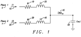
- FIG. 1 illustrates two phases, Phase 1 5 and Phase 2 7, with an equivalent model of two inductors in parallel.
- the first phase current, Phase 1 5, is defined as 11 15.
- the second phase current, Phase 2 7, is defined as 12 25.
- the equivalent model for the first inductor is shown as resistor element R1 10, and inductor L1 20.
- the equivalent model for the second inductor is shown as resistor element R2 30, and inductor L2 40.
- the resistor R1 10, and resistor R2 30 include the inductor DC resistance and output switch resistance of switching regulators.
- the first and second current, 11 15and 12 25, respectively sum to establish the output current I OUT, which flows into capacitor load C out 50 and Rload.
- resistance R1 and resistance R2 are of equal magnitude, then the current is split equally between the two phases, will minimize DC resistive loss. If the resistance R1 and resistance R2 are non-identical (and not equal), DC resistance loss, the same 11 and 12 current will not minimize.
- U. S. Patent 8,487,477 to Heineman shows a plurality of phases, a power stage, a feedback to balance the currents in the inductors.
- This circuit comprises a PID filter, a PWM, output control, power switches, load capacitor, and inductor and a feedback error amplifier to the PID filter.
- phase sharing has also been discussed in switching regulators.
- U. S. Patent 8,405,368 to Laur et al. has a multiple phases, multiple loads, and a phase current sharing solution.
- the phase current sharing network includes conversion networks, and phase current combining networks.
- U.S. Patent 8,330,438 to Sreenivas et al. describes a means of a system and a methodology for current balancing in a multi-phase buck converter.
- the circuit comprises output voltage controller, and plurality of inductors, low pass filters, and phase balance networks.
- a principal object of the present disclosure is to provide a circuit that can intentionally be used for imbalanced phase current.
- a principal object of the present disclosure is to provide a circuit that can intentionally change phase current to optimize efficiency in a multi-phase regulator with different inductors.
- a multi-phase switch regulator with improved efficiency comprising a pulse width modulation (PWM) control circuit which is configured to generate a PWM signal for each phase, a driver control network electrically coupled to said pulse width modulation (PWM) control circuit configured to receive a PWM signal (from said pulse width modulation (PWM) control circuit), an output stage electrically coupled to said driver configured to provide an output, a current sense circuit electrically coupled to said output stage configured to provide a phase current sense information, a current share circuit configured to receive the current signal from said current sense circuit and to provide a current share offset to said pulse width modulation (PWM) controller circuit for current balancing, and, a trim circuit electrically connected to said current sense circuit.
- PWM pulse width modulation
- the device is a multi-phase switch regulator with improved efficiency, the device comprising a pulse width modulation (PWM) control circuit configured to generate PWM signal for each phase, a driver control network electrically coupled to said pulse width modulation (PWM) control circuit configured to receive a PWM signal (signal from said pulse width modulation (PWM) control circuit), an output stage electrically coupled to said driver configured to provide an output, a dummy output stage configured to receive driver signals from said driver control network, a low pass filter (LPF) electrically coupled to the output of a dummy driver output stage, a current share circuit configured to receive a low pass filter (LPF) signal from said low pass filter (LPF) and providing an low pass filter (LPF) output signal to said pulse width modulation (PWM) control circuit for current balancing.
- PWM pulse width modulation
- a method of current sharing in a multi-phase switch regulator comprising the steps of (1) providing a system with current sharing function comprising a driver circuit, a current sense circuit, a current share circuit, a PWM control circuit, and a trim circuit, (2) providing said current sense circuit for each phase of said driver circuit, (3) sensing a signal using said current sense circuit for each phase of said driver circuit, (4) comparing the output of said current sense circuits, (5) generating a PWM drive signal, and, (6) equalizing the output of the current sense amplifier.
- a method of current sharing in a multi-phase switch regulator comprising the steps of (1) providing an adaptive current sharing optimization system comprising a driver circuit, an output stage, a dummy output stage, a low pass filter, a current share circuit, and a PWM control circuit, (2) driving a signal to said dummy output stage, (3) filtering a signal of said dummy output stage, (4) providing signals to said current share circuit, (5) providing the current error information to said PWM control circuit, and, (6) generating a PWM drive signal of each phase.
- FIG. 1 shows the resistance and inductance of the two inductor two phase multi-phase switcher elements in accordance with prior art embodiment.
- the first phase current, from Phase 1, 5 is 11 15.
- the second phase current, from Phase 2 7, is 12 25.
- the equivalent model for the first inductor is shown as resistor element R1 10, and inductor L1 20.
- the equivalent model for the second inductor is shown as resistor element R2 30, and inductor L2 40.
- the resistor R1 10, and resistor R2 30 includes the inductor DC resistance and output switch resistance of switching regulators.
- resistance R1 10 and resistance R2 30 are of equal magnitude, then the current is split equally between the two phases will minimize DC resistive loss. If the resistance R1 and resistance R2 are non-identical (and not equal), the same 11 and 12 current will minimize.
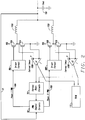
- FIG. 2 is a circuit schematic of a first embodiment with current sense circuitry and trim function circuitry.
- a function is implemented which can arbitrarily set the current sharing ratio of each phase where the current sharing can be achieved with different inductors, or different switch sizes on the output stage.
- the inductor elements are external components.
- the inductors are not a fixed size element, but can vary by application. As a result, the adjustments to the application can be done after device personalization and customization. This can be done by trimming with laser/ non-volatile memory or a digital interface.
- the embodiment in FIG. 2 can have the following features of (1) sensing the current in each phase, (2) current sense gain modified by the user by trimming or digital interface, and (3) a current feedback circuit which controls current sharing by adding an offset for each PWM signal in each phase (e.g. to keep/control each current snese output same.
- a multi-phase switch regulator is discussed.
- a multi-phase switch regulator with improved efficiency comprising a pulse width modulation (PWM) control circuit which is configured to generate a PWM signal for each phase, a driver control network electrically coupled to said pulse width modulation (PWM) control circuit configured to receive a PWM signal (from said pulse width modulation (PWM) control circuit), an output stage electrically coupled to said driver configured to provide an output, a current sense circuit electrically coupled to said output stage configured to provide a phase current sense information, a current share circuit configured to receive the current sense circuit output signal from said current sense circuit and to provide a current share offset to said pulse width modulation (PWM) controller circuit for current balancing, and, a trim circuit electrically connected to said current sense circuit.
- PWM pulse width modulation
- FIG. 2 shows the circuit schematic of the first embodiment of a two-phase buck converter. Note that this can be applicable to any number of phases, and other converter topologies such as boost, and buck-boost converter.
- the circuit comprises a pulse width modulation (PWM) controller circuit 60 which generates the Phase1 PWM signal 65A and Phase 2 PWM signal 65B.
- a feedback signal 61 from the output is an input to the PWM control circuit 60.
- the PWM control circuit 60 receives a signal from the current share circuit 70.
- the Phase 1 PWM signal 65A is coupled to the driver network 80A .
- the Phase 2 PWM signal 65B is coupled to the driver network 80B.
- the driver network 80A provides signals to the driver output stage, for p-channel MOSFET pull-up 90A, and n-channel MOSFET pull-down 91A.
- the driver network 80B provides signals to the driver output stage, for p-channel MOSFET pull-up 90B, and n-channel MOSFET pull-down 91B.
- Current sense circuit for the Phase 1 network is a variable amplifier 100A coupled to the n-channel MOSFET pull-down 91A.
- Current sense circuit for the Phase 2 network is a variable amplifier 100B coupled to the n-channel MOSFET pull-down 91B.
- the output signal of current sense amplifier 100A is coupled to the current share circuit 70.
- the output signal of current sense amplifier 100B is coupled to the current share circuit 70.
- the current sense amplifier 100A and current sense amplifier 100B are electrically coupled to the trim circuit 110.
- At the driver stage output of the Phase 1 network is an inductor 120A.
- At the driver stage output, of the Phase 2 network is an inductor 120B. Both inductors 120A and 120B are electrically connected to the output, and output capacitor Cout 150.
- the current sense circuit amplifies the sensed current or sensed voltage.
- the current sense amplifier is a variable gain amplifier which for the gain can be changed independent of each phase.
- Current sharing circuitry compares the output of current sense circuits and provides the current error information to the PWM controller.
- the PWM controller generates appropriate PWM drive signal for each phase, making the current sense amplifier (e.g. variable gain amplifier) output of the same value. If the gain of the variable gain amplifier A1 (Phase 1) 100A and variable gain amplifier A2 (Phase 2) 100B are the same magnitude, then the current share circuit (e.g. the feedback) will keep the phase current the same. If the gain values of the two amplifiers are different, the current share circuit will achieve a different current ratio current share function.
- the current sensing is done by the low-side switch voltage drop (.e.g. the n-channel MOSFET pull-down device) . Note that this can be done with a high-side switch voltage drop (e.g. the p-channel MOSFET pull-up device)., or a external current sense resistor between the inductor element and the output capacitor, or other current sense methodologies. Additionally, the current sense network can add variable gain amplifiers on each output of the current sense circuit. The variable gain amplifier control is established by the user using either trimming, or by a digital interface.
- FIG. 3 is a circuit schematic of a driver output stage and inductor equivalent model.
- FIG. 3 shows the output stage of the driver network, the input signals to the gates of the driver stage, and inductive/resistive load.
- the equivalent model for the inductor is shown as an inductor 220, and a resistor 221.
- the output driver controls to the MOSFET gates consist of control network 280, comprising a PWM signal and the duty factor (D) signal.
- the output stage of the driver has a pull-up p-channel MOSFET 290, and a pull-down n-channel MOSFET 291.
- Current sharing circuitry compares the output of current sense circuits and provides the current error information to PWM controller.
- the PWM controller generates an appropriate PWM drive signal for each phase, making the current sense amplifier (e.g. variable gain amplifier) output of the same value. If the gain of the variable gain amplifiers are the same magnitude, then the current share circuit (e.g. the feedback) will keep the phase current the same. If the gain values of the two amplifiers are different, the current share circuit will achieve a different current ratio current share function.
- the ratio is set by trimming, or established by a digital / analog interface according to the DC resistance difference between the phases. Given the device has a function to estimate the DC resistance, then the current sharing ratio can change adaptively according to the DC resistance.
- the MOSFET drain-to-source on-resistance of the p-channel pull-up MOSFET 290 can be expressed as Rds-on p.
- the MOSFET drain-to-source on resistance of the n-channel pull-up MOSFET 291 can be expressed as Rds-on n.
- switching devices may provide improved overall efficiency.
- the DC resistance of each phase will have a larger difference, and with optimization, can lead to improved efficiency.
- the gain of current sense amplifier in phase 1 should be 5/3 times higher than other phase current sense amplifier gain.
- the power loss can be reduced by 83mW with the embodiment in the disclosure.
- the conduction loss can be reduced 5% in this case, if current share circuit set phase 1 current as 60% of other phase current.
- using different size or type of output stage devices (switching devices) may provide a better overall efficiency. In this case, the DC resistance of each phase will have larger difference, and if it is optimized, the current can effectively improve the efficiency.
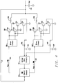
- FIG. 4 is a circuit schematic of a second embodiment with a dummy output stage.
- FIG. 4 shows the circuit schematic of an embodiment for a two-phase buck converter.
- the device is a multi-phase switch regulator with improved efficiency, the device comprising a pulse width modulation (PWM) control circuit configured to generate PWM signal for each phase, a driver control network electrically coupled to said pulse width modulation (PWM) control circuit configured to receive a PWM signal (signal from said pulse width modulation (PWM) control circuit), an output stage electrically coupled to said driver configured to provide an output, a dummy output stage configured to receive driver signals from said driver control network, a low pass filter (LPF) electrically coupled to the output of a dummy driver output stage, a current share circuit configured to receive a low pass filter (LPF) signal from said low pass filter (LPF) and providing an low pass filter (LPF) output signal to said pulse width modulation (PWM) control circuit for current balancing.
- PWM pulse width modulation
- the circuit comprises a pulse width modulation (PWM) controller circuit 60 which generates the Phase1 PWM signal 65A and Phase 2 PWM signal 65B.
- PWM pulse width modulation
- a feedback signal 61 from the output is an input to the PWM control circuits 60.
- the PWM control circuit 60 receives its signal from the current share circuit 70.
- the Phase 1 PWM signal 65A is coupled to the driver network 80A .
- the Phase 2 PWM signal 65B is coupled to the driver network 80B.
- the driver network 80A provides signals to the driver output stage, for p-channel MOSFET pull-up 90A, and n-channel MOSFET pull-down 91A, and dummy driver output stage p-channel MOSFET pull-up 92A and n-channel MOSFET pull-down 93A.
- the driver network 80B provides signals to the driver output stage, for p-channel MOSFET pull-up 90B, and n-channel MOSFET pull-down 91B, and dummy driver output stage p-channel MOSFET pull-up 92B and n-channel MOSFET pull-down 93B.
- the output of the dummy output stage formed with stage p-channel MOSFET pull-up 92A and n-channel MOSFET pull-down 93A is connected to a low pass filter (LPF) of resistor element 94A and capacitor element 95A.
- the output of the dummy output stage formed with stage p-channel MOSFET pull-up 92B and n-channel MOSFET pull-down 93B is connected to a low pass filter (LPF) of resistor element 94B and capacitor element 95B.
- the output signal of the low pass filter (LPF) of resistor element 94A and capacitor element 95A is coupled to the current share circuit 70.
- the output signal of low pass filter (LPF) of resistor element 94B and capacitor element 95B is coupled to the current share circuit 70.
- LPF low pass filter
- At the driver stage output of the Phase 1 network is an inductor 120A.
- At the driver stage output of the Phase 2 network is an inductor 120B. Both inductors 120A and 120B are electrically connected to the output, and output capacitor Cout 150.
- any network that provides the function for a low pass filter can achieve equivalent results.
- the resistor element and the capacitor element can be implemented using passive or active elements, including metal oxide semiconductor (MOS) field effect transistors.
- MOS metal oxide semiconductor
- the low pass filter network can include LC elements instead of RC elements.
- the filter network can also contain higher order filters.
- FIG. 5 is a method for a two phase switching regulator of a first embodiment.
- the methodology includes the steps, the first step 300 (1) providing a system with current sharing function comprising a driver circuit, a current sense circuit, a current share circuit, a PWM control circuit, and a trim circuit ; the second step 310 (2) providing said current sense circuit for each phase of said driver circuit; the third step 320 (3) sensing a signal using said current sense circuit for each phase of said driver circuit; fourth step 330 (4) comparing the output of said current sense circuits; the fifth step 340 (5) generating a PWM drive signal, and last step 350 (6) equalizing the output of the current sense amplifier.
- FIG. 6 is a method for a two phase switching regulator of a second embodiment.
- the methodology includes the steps, the first step 400 (1) providing an adaptive current sharing optimization system comprising a driver circuit, an output stage, a dummy output stage, a low pass filter, a current share circuit, and a PWM control circuit ; the second step 410, (2) driving a signal to said dummy output stage; the third step 420 (3) filtering a signal of said dummy output stage; fourth step 430 (4) providing signals to said current share circuit; the fifth step 440 (5) providing the current error information to said PWM control circuit, and last step 450 (6) generating a PWM drive signal of each phase.
- Each output stage has a dummy output stage and its output is averaged by filters.
- the filters can be low pass RC filters, of LC filters.
- the dummy output stage samples the current in the output driver. Since the role of the dummy output stage is to sample the current in the output driver network, the physical size of the sample network can be small. As a result, the addition of the dummy output stage, and the physical size of the p-channel MOSFET pull-up and the n-channel MOSFET pull-down can be small. Using a small dummy output stage, the area used to implement this additional elements can use minimum silicon area.
- the multi-phase switch regulator can be defined using bipolar transistors, or metal oxide semiconductor field effect transistors (MOSFETs).
- the switching regulator can be formed in a complementary metal oxide semiconductor (CMOS) technology and utilize p-channel and n-channel field effect transistors (e.g. PFETs and NFETs, respectively).
- CMOS complementary metal oxide semiconductor
- the regulator can be formed in a bipolar technology utilizing homo-junction bipolar junction transistors (BJT), or hetero-junction bipolar transistors (HBT) devices.
- BJT homo-junction bipolar junction transistors
- HBT hetero-junction bipolar transistors
- the switch regulator can be formed in a power technology utilizing lateral diffused metal oxide semiconductor (LDMOS) devices .
- the LDMOS devices can be an n-type LDMOS (NDMOS), or p-type LDMOS (PDMOS).
- the switch regulator can be formed in a bipolar-CMOS (BiCMOS) technology, or a bipolar
- a multi-phase switch regulator with improved efficiency are herein described.
- the improvement is achieved with minimal impact on silicon area or power usage.
- the multi-phase switcher improves efficiency with the introduction of current sense networks, current share balancing, trim circuitry, and dummy output stage methods.
Landscapes
- Engineering & Computer Science (AREA)
- Power Engineering (AREA)
- Dc-Dc Converters (AREA)
Abstract
Description
- The disclosure relates generally to a multi-phase switching regulator circuits and, more particularly, to a multi-phase switching regulator device having improved current sharing function thereof.
- Multi-phase switching regulators, sometimes known as a multi-phase switcher, is designed to distribute the output current evenly for each phase.. In steady state operation, each phase has an equal amount of current. Some of the multi-phase switcher devices have the current sharing circuit which equalizes the current in each phase using a feedback mechanism. With equal current in each phase, the highest conversion efficiency is achieved when all phases are identical and symmetric; this is achieved with the same output stage switch, and the same inductor element.
- In systems today, some of the multi-phase switch regulators have a "phase shedding" function. The phase shedding function reduces the number of active phases when the external load is light. For example, for the light load case, typically only one phase is operating, and all other phases will stop switching. In the multi-phase switch regulators, with phase shedding function, using the same inductor element for all the phases may be an optimum solution. For example, the efficiency can be improved using a low alternating current (AC) loss inductor during light load applications. During light load conditions, in
phase 1 operation, the alternating current (AC) loss is dominated by inductor core loss. In contrast, usage of a low direct current (DC) loss inductor for the other phases improves the efficiency at heavy load conditions. For heavy load conditions, the conduction loss (e.g. IR loss) is dominant in the heavy load conditions. - Inductors are non-ideal and contain inductive, resistive and capacitive electrical characteristics. Different type of inductors typically have different DC and AC resistance . Current equalization in each phase of a multi-phase switch regulator is not optimum.
- To illustrate the influence of resistance of inductor elements on multi-phase switch regulators, an example of a two-phase multi-phase switcher is shown.
FIG. 1 illustrates two phases,Phase 1 5 andPhase 2 7, with an equivalent model of two inductors in parallel. The first phase current,Phase 1 5, is defined as 11 15. The second phase current,Phase 2 7, is defined as 12 25. The equivalent model for the first inductor is shown asresistor element R1 10, andinductor L1 20. The equivalent model for the second inductor is shown asresistor element R2 30, and inductor L2 40. Theresistor R1 10, and resistor R2 30 include the inductor DC resistance and output switch resistance of switching regulators. The first and second current, 11 15and 12 25, respectively sum to establish the output current I OUT, which flows into capacitor load C out 50 and Rload. The optimum current 11 15 and 12 25 to minimize the loss can be expressed as follows:

- If the resistance R1 and resistance R2 are of equal magnitude, then the current is split equally between the two phases, will minimize DC resistive loss. If the resistance R1 and resistance R2 are non-identical (and not equal), DC resistance loss, the same 11 and 12 current will not minimize.
- Concepts for detection and current balancing has been discussed in DC-DC converter circuits.
U.S. Patent 8,502,515 to Wan et al , describes a DC-DC converter having a load, a current detecting circuit and a channel current balance circuit. - Implementations to discuss proper ramping of current sharing also has been disclosed.
U. S. Patent 8,487,477 to Heineman shows a plurality of phases, a power stage, a feedback to balance the currents in the inductors. This circuit comprises a PID filter, a PWM, output control, power switches, load capacitor, and inductor and a feedback error amplifier to the PID filter. - Phase sharing has also been discussed in switching regulators.
U. S. Patent 8,405,368 to Laur et al. has a multiple phases, multiple loads, and a phase current sharing solution. The phase current sharing network includes conversion networks, and phase current combining networks. - Current balancing has also been discussed in multi-phase buck converters.
U.S. Patent 8,330,439 to Wu et al. shows a system and a methodology for current balancing in a multi-phase buck converter. The system includes power stages, inductors error amplifiers, PFM/PWM transition logic and power stage control logic. - Other concepts have also been proposed in multiple switch converters.
U.S. Patent 8,330,438 to Sreenivas et al. describes a means of a system and a methodology for current balancing in a multi-phase buck converter. The circuit comprises output voltage controller, and plurality of inductors, low pass filters, and phase balance networks. - It is desirable to provide a solution to address the disadvantages of current balancing and efficiency in a multi-phase switching regulator.
- A principal object of the present disclosure is to provide a circuit that can intentionally be used for imbalanced phase current.
- A principal object of the present disclosure is to provide a circuit that can intentionally change phase current to optimize efficiency in a multi-phase regulator with different inductors.
- The above and other objects are achieved by a multi-phase regulator with different inductors.
- In addition, a device is disclosed in accordance with the embodiment of the disclosure. A multi-phase switch regulator with improved efficiency, the device comprising
a pulse width modulation (PWM) control circuit which is configured to generate a PWM signal for each phase, a driver control network electrically coupled to said pulse width modulation (PWM) control circuit configured to receive a PWM signal (from said pulse width modulation (PWM) control circuit), an output stage electrically coupled to said driver configured to provide an output, a current sense circuit electrically coupled to said output stage configured to provide a phase current sense information, a current share circuit configured to receive the current signal from said current sense circuit and to provide a current share offset to said pulse width modulation (PWM) controller circuit for current balancing, and, a trim circuit electrically connected to said current sense circuit. - In addition, a device is disclosed in accordance with the embodiment of the disclosure. The device is a multi-phase switch regulator with improved efficiency, the device comprising a pulse width modulation (PWM) control circuit configured to generate PWM signal for each phase, a driver control network electrically coupled to said pulse width modulation (PWM) control circuit configured to receive a PWM signal (signal from said pulse width modulation (PWM) control circuit), an output stage electrically coupled to said driver configured to provide an output, a dummy output stage configured to receive driver signals from said driver control network, a low pass filter (LPF) electrically coupled to the output of a dummy driver output stage, a current share circuit configured to receive a low pass filter (LPF) signal from said low pass filter (LPF) and providing an low pass filter (LPF) output signal to said pulse width modulation (PWM) control circuit for current balancing.
- In addition, a method is disclosed in accordance with the embodiment of the disclosure. A method of current sharing in a multi-phase switch regulator comprising the steps of (1) providing a system with current sharing function comprising a driver circuit, a current sense circuit, a current share circuit, a PWM control circuit, and a trim circuit, (2) providing said current sense circuit for each phase of said driver circuit, (3) sensing a signal using said current sense circuit for each phase of said driver circuit, (4) comparing the output of said current sense circuits, (5) generating a PWM drive signal, and, (6) equalizing the output of the current sense amplifier.
- In addition, a method is disclosed in accordance with the embodiment of the disclosure. A method of current sharing in a multi-phase switch regulator comprising the steps of (1) providing an adaptive current sharing optimization system comprising a driver circuit, an output stage, a dummy output stage, a low pass filter, a current share circuit, and a PWM control circuit, (2) driving a signal to said dummy output stage, (3) filtering a signal of said dummy output stage, (4) providing signals to said current share circuit, (5) providing the current error information to said PWM control circuit, and, (6) generating a PWM drive signal of each phase.
- As such, a novel multi-phase switching regulator with improved efficiency is disclosed. Other advantages will be recognized by those of ordinary skill in the art.
- The present disclosure and the corresponding advantages and features provided thereby will be best understood and appreciated upon review of the following detailed description of the disclosure, taken in conjunction with the following drawings, where like numerals represent like elements, in which:
-
FIG. 1 is a circuit schematic of a two phase switching regulator inductor equivalent model; -
FIG. 2 is a circuit schematic of a first embodiment with current sense circuitry and trim function circuitry; -
FIG. 3 is a circuit schematic of a driver output stage and inductor equivalent model; -
FIG. 4 is a circuit schematic of a second embodiment with a dummy output stage; -
FIG. 5 is a method for a two phase switching regulator of a first embodiment; and, -
FIG. 6 is a method for a two phase switching regulator of a second embodiment. - To illustrate the influence of resistance of inductor elements on multi-phase switch regulators, an example of a two-phase multi-phase switcher is shown.
FIG. 1 shows the resistance and inductance of the two inductor two phase multi-phase switcher elements in accordance with prior art embodiment. The first phase current, fromPhase Phase 2 7, is 12 25. The equivalent model for the first inductor is shown asresistor element R1 10, andinductor L1 20. The equivalent model for the second inductor is shown asresistor element R2 30, and inductor L2 40. Theresistor R1 10, andresistor R2 30 includes the inductor DC resistance and output switch resistance of switching regulators. The first and second current, 1115and 12 25, respectively sum to establish the output current I OUT 45, which flows into capacitor load C out 50 and Rload. The optimum current 1115and I2 25 to minimize the loss can be expressed as follows:

- If the
resistance R1 10 andresistance R2 30 are of equal magnitude, then the current is split equally between the two phases will minimize DC resistive loss. If the resistance R1 and resistance R2 are non-identical (and not equal), the same 11 and 12 current will minimize. -
FIG. 2 is a circuit schematic of a first embodiment with current sense circuitry and trim function circuitry. In this embodiment, a function is implemented which can arbitrarily set the current sharing ratio of each phase where the current sharing can be achieved with different inductors, or different switch sizes on the output stage. - The inductor elements are external components. The inductors are not a fixed size element, but can vary by application. As a result, the adjustments to the application can be done after device personalization and customization. This can be done by trimming with laser/ non-volatile memory or a digital interface. The embodiment in
FIG. 2 can have the following features of (1) sensing the current in each phase, (2) current sense gain modified by the user by trimming or digital interface, and (3) a current feedback circuit which controls current sharing by adding an offset for each PWM signal in each phase (e.g. to keep/control each current snese output same. In this embodiment, a multi-phase switch regulator is discussed. A multi-phase switch regulator with improved efficiency, the device comprising a pulse width modulation (PWM) control circuit which is configured to generate a PWM signal for each phase, a driver control network electrically coupled to said pulse width modulation (PWM) control circuit configured to receive a PWM signal (from said pulse width modulation (PWM) control circuit), an output stage electrically coupled to said driver configured to provide an output, a current sense circuit electrically coupled to said output stage configured to provide a phase current sense information, a current share circuit configured to receive the current sense circuit output signal from said current sense circuit and to provide a current share offset to said pulse width modulation (PWM) controller circuit for current balancing, and, a trim circuit electrically connected to said current sense circuit. -
FIG. 2 shows the circuit schematic of the first embodiment of a two-phase buck converter. Note that this can be applicable to any number of phases, and other converter topologies such as boost, and buck-boost converter. In this example of a two-phase buck converter, the circuit comprises a pulse width modulation (PWM)controller circuit 60 which generates thePhase1 PWM signal 65A andPhase 2PWM signal 65B. Afeedback signal 61 from the output is an input to thePWM control circuit 60. ThePWM control circuit 60 receives a signal from thecurrent share circuit 70. ThePhase 1PWM signal 65A is coupled to thedriver network 80A . ThePhase 2PWM signal 65B is coupled to thedriver network 80B. Thedriver network 80A provides signals to the driver output stage, for p-channel MOSFET pull-up 90A, and n-channel MOSFET pull-down 91A. Thedriver network 80B provides signals to the driver output stage, for p-channel MOSFET pull-up 90B, and n-channel MOSFET pull-down 91B. Current sense circuit for thePhase 1 network is avariable amplifier 100A coupled to the n-channel MOSFET pull-down 91A. Current sense circuit for thePhase 2 network is avariable amplifier 100B coupled to the n-channel MOSFET pull-down 91B. The output signal ofcurrent sense amplifier 100A is coupled to thecurrent share circuit 70. The output signal ofcurrent sense amplifier 100B is coupled to thecurrent share circuit 70. Thecurrent sense amplifier 100A andcurrent sense amplifier 100B are electrically coupled to thetrim circuit 110. At the driver stage output of thePhase 1 network is aninductor 120A. At the driver stage output, of thePhase 2 network is aninductor 120B. Bothinductors output capacitor Cout 150. - The current sense circuit amplifies the sensed current or sensed voltage. In this embodiment, the current sense amplifier is a variable gain amplifier which for the gain can be changed independent of each phase. Current sharing circuitry compares the output of current sense circuits and provides the current error information to the PWM controller. The PWM controller generates appropriate PWM drive signal for each phase, making the current sense amplifier (e.g. variable gain amplifier) output of the same value. If the gain of the variable gain amplifier A1 (Phase 1) 100A and variable gain amplifier A2 (Phase 2) 100B are the same magnitude, then the current share circuit (e.g. the feedback) will keep the phase current the same. If the gain values of the two amplifiers are different, the current share circuit will achieve a different current ratio current share function.
- In the embodiment illustrated in
FIG.2 , the current sensing is done by the low-side switch voltage drop (.e.g. the n-channel MOSFET pull-down device) . Note that this can be done with a high-side switch voltage drop (e.g. the p-channel MOSFET pull-up device)., or a external current sense resistor between the inductor element and the output capacitor, or other current sense methodologies. Additionally, the current sense network can add variable gain amplifiers on each output of the current sense circuit. The variable gain amplifier control is established by the user using either trimming, or by a digital interface. -
FIG. 3 is a circuit schematic of a driver output stage and inductor equivalent model.FIG. 3 shows the output stage of the driver network, the input signals to the gates of the driver stage, and inductive/resistive load. The equivalent model for the inductor is shown as aninductor 220, and aresistor 221. The output driver controls to the MOSFET gates consist ofcontrol network 280, comprising a PWM signal and the duty factor (D) signal. The output stage of the driver has a pull-up p-channel MOSFET 290, and a pull-down n-channel MOSFET 291. Current sharing circuitry compares the output of current sense circuits and provides the current error information to PWM controller. The PWM controller generates an appropriate PWM drive signal for each phase, making the current sense amplifier (e.g. variable gain amplifier) output of the same value. If the gain of the variable gain amplifiers are the same magnitude, then the current share circuit (e.g. the feedback) will keep the phase current the same. If the gain values of the two amplifiers are different, the current share circuit will achieve a different current ratio current share function. The ratio is set by trimming, or established by a digital / analog interface according to the DC resistance difference between the phases. Given the device has a function to estimate the DC resistance, then the current sharing ratio can change adaptively according to the DC resistance. The MOSFET drain-to-source on-resistance of the p-channel pull-upMOSFET 290 can be expressed as Rds-on p. The MOSFET drain-to-source on resistance of the n-channel pull-upMOSFET 291 can be expressed as Rds-on n. The resistance for each phase can be calculated from the duty cycle (D), the inductor resistance, and the MOSFET drain-to-source on resistances, as follows:
- In some applications, using different size or type of output stage devices (switching devices) may provide improved overall efficiency. In this case, the DC resistance of each phase will have a larger difference, and with optimization, can lead to improved efficiency.
- As an example of the disclosed technique, An optimum current balance to minimize DC current can be calculated as follows:
If high side and low side switch Rds-on = 40mohm, and phase1 uses the inductor with 60mohm DC resistance, andphase 2∼4 use the inductor with 20mohm inductors.
Rdc1 = 100mohm,
Rdc2∼4 = 60mohm - Thus, optimum current sharing condition to minimize DC resistance
5/3 ∗ I1 = I2 = I3 = I4
(11 = 60% of 12, 13 and 14) - Therefore, the gain of current sense amplifier in
phase 1 should be 5/3 times higher than other phase current sense amplifier gain. The total DC loss with current invention will be:
Total 10A case,
If the current share trimming is set properly, each phase current will be:
If current is shared evenly, then
I1=I2=I3=I4=2.5A and the total DC loss = 1750mW (without this embodiment) - The power loss can be reduced by 83mW with the embodiment in the disclosure. The conduction loss can be reduced 5% in this case, if current share circuit set
phase 1 current as 60% of other phase current. In some applications, using different size or type of output stage devices (switching devices) may provide a better overall efficiency. In this case, the DC resistance of each phase will have larger difference, and if it is optimized, the current can effectively improve the efficiency. -
FIG. 4 is a circuit schematic of a second embodiment with a dummy output stage.FIG. 4 shows the circuit schematic of an embodiment for a two-phase buck converter. The device is a multi-phase switch regulator with improved efficiency, the device comprising a pulse width modulation (PWM) control circuit configured to generate PWM signal for each phase, a driver control network electrically coupled to said pulse width modulation (PWM) control circuit configured to receive a PWM signal (signal from said pulse width modulation (PWM) control circuit), an output stage electrically coupled to said driver configured to provide an output, a dummy output stage configured to receive driver signals from said driver control network, a low pass filter (LPF) electrically coupled to the output of a dummy driver output stage, a current share circuit configured to receive a low pass filter (LPF) signal from said low pass filter (LPF) and providing an low pass filter (LPF) output signal to said pulse width modulation (PWM) control circuit for current balancing. Note that this can be applicable to any number of phases, and other converter topologies such as boost, and buck-boost converters. In this example of a two-phase buck converter, the circuit comprises a pulse width modulation (PWM)controller circuit 60 which generates thePhase1 PWM signal 65A andPhase 2PWM signal 65B. Afeedback signal 61 from the output is an input to thePWM control circuits 60. ThePWM control circuit 60 receives its signal from thecurrent share circuit 70. ThePhase 1PWM signal 65A is coupled to thedriver network 80A . ThePhase 2PWM signal 65B is coupled to thedriver network 80B. Thedriver network 80A provides signals to the driver output stage, for p-channel MOSFET pull-up 90A, and n-channel MOSFET pull-down 91A, and dummy driver output stage p-channel MOSFET pull-up 92A and n-channel MOSFET pull-down 93A. Thedriver network 80B provides signals to the driver output stage, for p-channel MOSFET pull-up 90B, and n-channel MOSFET pull-down 91B, and dummy driver output stage p-channel MOSFET pull-up 92B and n-channel MOSFET pull-down 93B. The output of the dummy output stage formed with stage p-channel MOSFET pull-up 92A and n-channel MOSFET pull-down 93A is connected to a low pass filter (LPF) ofresistor element 94A andcapacitor element 95A. The output of the dummy output stage formed with stage p-channel MOSFET pull-up 92B and n-channel MOSFET pull-down 93B is connected to a low pass filter (LPF) ofresistor element 94B andcapacitor element 95B. The output signal of the low pass filter (LPF) ofresistor element 94A andcapacitor element 95A is coupled to thecurrent share circuit 70. The output signal of low pass filter (LPF) ofresistor element 94B andcapacitor element 95B is coupled to thecurrent share circuit 70. At the driver stage output of thePhase 1 network is aninductor 120A. At the driver stage output of thePhase 2 network is aninductor 120B. Bothinductors output capacitor Cout 150. - In this embodiment, any network that provides the function for a low pass filter can achieve equivalent results. The resistor element and the capacitor element can be implemented using passive or active elements, including metal oxide semiconductor (MOS) field effect transistors. The low pass filter network can include LC elements instead of RC elements. The filter network can also contain higher order filters.
-
FIG. 5 is a method for a two phase switching regulator of a first embodiment. The methodology includes the steps, the first step 300 (1) providing a system with current sharing function comprising a driver circuit, a current sense circuit, a current share circuit, a PWM control circuit, and a trim circuit ; the second step 310 (2) providing said current sense circuit for each phase of said driver circuit; the third step 320 (3) sensing a signal using said current sense circuit for each phase of said driver circuit; fourth step 330 (4) comparing the output of said current sense circuits; the fifth step 340 (5) generating a PWM drive signal, and last step 350 (6) equalizing the output of the current sense amplifier. -
FIG. 6 is a method for a two phase switching regulator of a second embodiment. The methodology includes the steps, the first step 400 (1) providing an adaptive current sharing optimization system comprising a driver circuit, an output stage, a dummy output stage, a low pass filter, a current share circuit, and a PWM control circuit ; thesecond step 410, (2) driving a signal to said dummy output stage; the third step 420 (3) filtering a signal of said dummy output stage; fourth step 430 (4) providing signals to said current share circuit; the fifth step 440 (5) providing the current error information to said PWM control circuit, and last step 450 (6) generating a PWM drive signal of each phase. - Each output stage has a dummy output stage and its output is averaged by filters. The filters can be low pass RC filters, of LC filters. The dummy output stage samples the current in the output driver. Since the role of the dummy output stage is to sample the current in the output driver network, the physical size of the sample network can be small. As a result, the addition of the dummy output stage, and the physical size of the p-channel MOSFET pull-up and the n-channel MOSFET pull-down can be small. Using a small dummy output stage, the area used to implement this additional elements can use minimum silicon area.
- The averaged voltage of the dummy output stage can be calculated as
Phase 1: Vave1 = D1 x Vin Phase 2: Vave2 = D2 x Vin
The voltage drop due to the output current in the main stage output for each phase can be calculated as

Phase 1: Vave1 = R1 x 11 + Vout Phase 2: Vave2 = R2 x 12 + Vout 


- The multi-phase switch regulator can be defined using bipolar transistors, or metal oxide semiconductor field effect transistors (MOSFETs). The switching regulator can be formed in a complementary metal oxide semiconductor (CMOS) technology and utilize p-channel and n-channel field effect transistors (e.g. PFETs and NFETs, respectively). The regulator can be formed in a bipolar technology utilizing homo-junction bipolar junction transistors (BJT), or hetero-junction bipolar transistors (HBT) devices. The switch regulator can be formed in a power technology utilizing lateral diffused metal oxide semiconductor (LDMOS) devices . The LDMOS devices can be an n-type LDMOS (NDMOS), or p-type LDMOS (PDMOS). The switch regulator can be formed in a bipolar-CMOS (BiCMOS) technology, or a bipolar-CMOS-DMOS (BCD) technology.
- As such, a multi-phase switch regulator with improved efficiency are herein described. The improvement is achieved with minimal impact on silicon area or power usage. The multi-phase switcher improves efficiency with the introduction of current sense networks, current share balancing, trim circuitry, and dummy output stage methods. Other advantages will be recognized by those of ordinary skill in the art. The above detailed description of the disclosure, and the examples described therein, has been presented for the purposes of illustration and description. While the principles of the disclosure have been described above in connection with a specific device, it is to be clearly understood that this description is made only by way of example and not as a limitation on the scope of the disclosure.
-
- 1. A multi-phase switch regulator with improved efficiency, the device comprising:
- a pulse width modulation (PWM) control circuit which is configured to generate a PWM signal for each phase ;
- a driver control network electrically coupled to said pulse width modulation (PWM) control circuit configured to receive a PWM signal (from said pulse width modulation (PWM) control circuit);
- an output stage electrically coupled to said driver circuit control configured to provide an output;
- a current sense circuit electrically coupled to said output stage configured to provide current sense information;
- a current share circuit configured to receive the current sense output signal from said current sense circuit and to provide a current share offset to said pulse width modulation (PWM) control circuit for current balancing; and,
- a trim circuit electrically connected to said current sense circuit.
- 2. The multi-phase switch regulator of
embodiment 1 wherein said multi-phase switch regulator has a plurality of phases and said driver control stage, said output stage, and current sense circuit for each phase. - 3. The multi-phase switch regulator of
embodiment 1, wherein said output stage is electrically connected to an inductor. - 4. The multi-phase switch regulator of embodiment 3, wherein said current sense circuit is a variable gain amplifier.
- 5. The multi-phase switch regulator of embodiment 4, wherein said variable gain amplifier can be customized or personalized with said trim circuit, e.g. by laser/non-volatile
memory, or digital interface. - 6. The multi-phase switch regulator of
embodiment 1 wherein said current share circuit provides current sharing by adding offset for each said PWM phase signal to keep and control each current sense output at an equal magnitude. - 7. A multi-phase switch regulator with improved efficiency, the device comprising:
- a pulse width modulation (PWM) control circuit configured to generate a PWM signal for each phase;
- a driver control network electrically coupled to said pulse width modulation (PWM) control circuit configured to receive a PWM signal (signal from said pulse width modulation (PWM) control circuit);
- an output stage electrically coupled to said driver control network configured to provide an output;
- a dummy output stage configured to receive driver signals from said driver control network;
- a low pass filter (LPF) electrically coupled to the output of a dummy output stage;
- a current share circuit configured to receive a low pass filter (LPF) output signal from said low pass filter (LPF) and to provide an low pass filter (LPF) output signal to said pulse width modulation (PWM) control circuit for current balancing.
- 8. The multi-phase switch regulator of
embodiment 7, wherein said low pass filter (LPF) is a resistor-capacitor (RC) filter, or a an inductor-capacitor (LC) filter. - 9. A method of current sharing in a multi-phase switch regulator comprising the steps of:
- providing a system with current sharing function comprising a driver circuit, a current sense circuit, a current share circuit, a PWM control circuit, and a trim circuit;
- providing said current sense circuit for each phase of said driver circuit;
- sensing a signal using said current sense circuit for each phase of said driver circuit;
- comparing the output of said current sense circuits;
- generating a PWM drive signal; and,
- equalizing the output of the current sense amplifier.
- 10. A method of current sharing in a multi-phase switch regulator comprising the steps of:
- providing an adaptive current sharing optimization system comprising a driver circuit, an output stage, a dummy output stage, a low pass filter, a current share circuit, and a PWM control circuit;
- driving a signal to said dummy driver output stage;
- filtering a signal of said dummy driver output stage;
- providing signals to said current share circuit;
- providing the current error information to said PWM control circuit; and,
- generating a PWM drive signal of each phase.
- 11. The method of
embodiment 9 or 10 wherein said multi-phase switch regulator comprises a low pass filter (LPF). - 12. The method of embodiment 11, wherein said low pass filter (LPF) is a resistor-capacitor (RC) filter.
- 13. The method of embodiment 11, wherein said low pass filter (LPF) is an inductor-capacitor (LC) filter.
- 14. The method of
embodiment 12, wherein said resistor-capacitor (RC) filter comprises
a plurality of resistor and capacitor elements. - 15. The method of embodiment 13, wherein said inductor-capacitor (LC) filter comprises a plurality of inductor and capacitor elements.
Claims (15)
- An apparatus, comprising:a first driver network (80A) configured to generate a first plurality of control signals for a first driver output stage (90A, 91A) based on a first pulse width control signal (65A), wherein the first driver output stage (90A, 91A) is coupled to an output node (150) via a first inductor (120A), and wherein the first driver network (80A) is configured to source, based on the first plurality of control signals, a first current to the output node (150) via the first inductor (120A);a second driver network (80B) configured to generate a second plurality of control signals for a second driver output stage (90B, 91B) based on a second pulse width control signal (65B), wherein the second driver output stage (90B, 91B) is coupled to the output node (150) via a second inductor (120B), wherein the second driver network (80B) is configured to source, based on the second plurality of control signals, a second current to the output node (150) via the second inductor (120B);a comparison circuit (70) configured to perform a comparison of the first current and the second current; anda pulse width modulation control circuit (60) configured to generate the first control pulse width modulation control signal (65A) and the second pulse width modulation control signal (65B) using results of the comparison of the first current and the second current.
- The apparatus of claim 1, further comprising:a first sense circuit (100A) configured to sense a value of the first current; anda second sense circuit (100B) configured to sense a value of the second current.
- The apparatus of claim 2, wherein the first sense circuit (100A) includes a first variable-gain amplifier circuit, and the second sense circuit (100B) includes a second variable-gain amplifier circuit, and further comprising a trim circuit (110) configured to adjust a gain of the first variable-gain amplifier circuit or a gain of the second variable-gain amplifier circuit.
- The apparatus of claim 3, wherein the trim circuit (110) is further configured to adjust the gain of the first variable-gain amplifier circuit and the gain of the second variable-gain amplifier circuit based on output resistance of the first driver network (80A) and an output resistance of the second driver network (80B).
- The apparatus of claim 2, wherein the first driver output stage (90A, 91A) includes a first device coupled between the first inductor (120A) and a ground supply node, and wherein to sense the value of the first current, the first sense circuit (100A) is configured to measure a current flowing in the first device.
- The apparatus of claim 1, wherein the pulse width modulation control circuit (60) is further configured to generate the first control pulse width modulation control signal (65A) and the second pulse width modulation control signal (65B) using results of the comparison of the first current and the second current and a feedback signal from the output node (61).
- The apparatus of claim 1, further comprising:a first dummy output circuit (92A, 93A) configured to generate a first dummy signal using the first plurality of control signals;a second dummy output circuit (92B, 93B) configured to generate a second dummy signal using the second plurality of control signals;wherein the comparison circuit (70) is further configured to perform a comparison of the first dummy signal and the second dummy signal; andwherein the pulse width modulation control circuit (80B) is further configured to generate the first pulse width modulation control signal (65A) and the second pulse width modulation control signal (65B) using results of the comparison of the first dummy current and the second dummy current.
- The apparatus of claim 7, further comprising:a first low-pass filter circuit configured to low-pass filter the first dummy signal; anda second low-pass filter circuit configured to low-pass filter the second dummy signal.
- The apparatus of claim 8, wherein the first low-pass filter circuit includes a first resistor-capacitor low-pass filter circuit, and wherein the second low-pass filter circuit includes a second resistor-capacitor low-pass filter circuit.
- A method, comprising:sourcing, by a first driver output stage (90A, 91A) and based on a first pulse width modulation control signal (65A), a first current to an output node (150) via a first inductor (120A);sourcing, by a second driver output stage (90B, 91B) and based on a second pulse width modulation control signal (65B), a second current to the output node (150) via a second inductor (120B);performing a comparison of the first current and the second current; andgenerating the first pulse width modulation control signal (65A) and the second pulse width modulation control signal (65B) using result of the comparison.
- The method of claim 10, further comprising:sensing, by a first sensing circuit (100A), a value of the first current; andsensing, by a second sensing circuit (100B), a value of the second current.
- The method of claim 11, wherein the first driver output stage includes a first device coupled between the first inductor and a ground supply node, and wherein sensing the value of the first current includes measuring a current flowing in the first device.
- The method of claim 11, wherein the first sensing circuit (100A) includes a first variable-gain amplifier circuit, and wherein the second sensing circuit (100B) includes a second variable-gain amplifier circuit, and further comprising:adjusting, by a trim circuit (110), a gain of the first variable-gain amplifier circuit; oradjusting, by the trim circuit (110), a gain of the second variable-gain amplifier circuit.
- The method of claim 13, further comprising:determining an output resistance of the first driver network (80A); andadjusting, by the trim circuit (110), the gain the first variable-gain amplifier circuit using the output resistance of the first driver network (80A).
- The method of claim 10, wherein the first control signal is a pulse width modulation control signal.
Priority Applications (1)
| Application Number | Priority Date | Filing Date | Title |
|---|---|---|---|
| EP20208063.6A EP3799285A1 (en) | 2014-08-14 | 2014-08-14 | An apparatus and method for current sharing in a multi-phase switching regulator |
Applications Claiming Priority (2)
| Application Number | Priority Date | Filing Date | Title |
|---|---|---|---|
| EP20208063.6A EP3799285A1 (en) | 2014-08-14 | 2014-08-14 | An apparatus and method for current sharing in a multi-phase switching regulator |
| EP14181098.6A EP2985899A1 (en) | 2014-08-14 | 2014-08-14 | An apparatus and method for current sharing in a multi-phase switching regulator |
Related Parent Applications (1)
| Application Number | Title | Priority Date | Filing Date |
|---|---|---|---|
| EP14181098.6A Division EP2985899A1 (en) | 2014-08-14 | 2014-08-14 | An apparatus and method for current sharing in a multi-phase switching regulator |
Publications (1)
| Publication Number | Publication Date |
|---|---|
| EP3799285A1 true EP3799285A1 (en) | 2021-03-31 |
Family
ID=51352440
Family Applications (2)
| Application Number | Title | Priority Date | Filing Date |
|---|---|---|---|
| EP14181098.6A Ceased EP2985899A1 (en) | 2014-08-14 | 2014-08-14 | An apparatus and method for current sharing in a multi-phase switching regulator |
| EP20208063.6A Ceased EP3799285A1 (en) | 2014-08-14 | 2014-08-14 | An apparatus and method for current sharing in a multi-phase switching regulator |
Family Applications Before (1)
| Application Number | Title | Priority Date | Filing Date |
|---|---|---|---|
| EP14181098.6A Ceased EP2985899A1 (en) | 2014-08-14 | 2014-08-14 | An apparatus and method for current sharing in a multi-phase switching regulator |
Country Status (2)
| Country | Link |
|---|---|
| US (1) | US9520788B2 (en) |
| EP (2) | EP2985899A1 (en) |
Families Citing this family (15)
| Publication number | Priority date | Publication date | Assignee | Title |
|---|---|---|---|---|
| DE102015200716A1 (en) * | 2015-01-19 | 2016-07-21 | Efficient Energy Gmbh | Switching Power Supply |
| US9627976B2 (en) | 2015-02-20 | 2017-04-18 | Linear Technology Corporation | Control architecture with improved transient response |
| US10050559B2 (en) | 2016-01-20 | 2018-08-14 | Linear Technology Llc | Control architecture with improved transient response |
| CN106156508B (en) * | 2016-06-30 | 2018-11-27 | 温州大学 | A kind of parallel operation system optimal point determines method |
| US10211728B2 (en) | 2017-03-02 | 2019-02-19 | Hong Kong Applied Science and Technology Research Institute Company, Limited | Current-sharing circuit for DC-DC converters |
| US10693361B2 (en) * | 2018-08-01 | 2020-06-23 | Infineon Technologies Austria Ag | Faulty current sense line detection in multiphase voltage regulators |
| US10749433B2 (en) * | 2018-09-14 | 2020-08-18 | Dialog Semiconductor (Uk) Limited | Current balance feedback circuit and method to improve the stability of a multi-phase converter |
| WO2020183823A1 (en) * | 2019-03-14 | 2020-09-17 | 株式会社村田製作所 | System power supply device |
| US11152846B2 (en) | 2020-01-15 | 2021-10-19 | Apple Inc. | Method and apparatus for providing adaptive inductor peak current in DC-DC converter |
| JP7298774B2 (en) * | 2020-03-26 | 2023-06-27 | 株式会社村田製作所 | Multi-converter power system |
| US11960434B2 (en) | 2021-04-07 | 2024-04-16 | Sony Semiconductor Solutions Corporation | Communication device, communication system, and communication method for transmitting data blocks including signal groups conforming to a serial peripheral interface |
| US12278551B2 (en) | 2022-04-01 | 2025-04-15 | Analog Devices, Inc | Trans-inductor voltage regulator current sensing techniques |
| US11979081B2 (en) | 2021-05-19 | 2024-05-07 | Analog Devices, Inc. | Current sensing techniques for power converter circuits |
| US11652415B2 (en) | 2021-05-19 | 2023-05-16 | Analog Devices, Inc. | Current sensing techniques for power converter circuits |
| CN119602601A (en) * | 2023-09-08 | 2025-03-11 | 立锜科技股份有限公司 | Conversion control circuit and method for stackable multi-phase power converter |
Citations (9)
| Publication number | Priority date | Publication date | Assignee | Title |
|---|---|---|---|---|
| US20040085789A1 (en) * | 2000-10-26 | 2004-05-06 | Laszlo Lipcsei | DC-to-DC converter with improved transient response |
| US20050225307A1 (en) * | 2004-04-12 | 2005-10-13 | Tetsuo Sato | Current sensing circuit for a multi-phase DC-DC converter |
| US7508182B1 (en) * | 2005-10-26 | 2009-03-24 | Semtech Corporation | Method and apparatus for improved current mode control for large conversion ratio synchronous buck converter with lossless current sense |
| US8330438B2 (en) | 2007-08-30 | 2012-12-11 | International Rectifier Corporation | Method and apparatus for equalizing phase currents in multiphase switching power converters |
| US8330439B2 (en) | 2009-06-23 | 2012-12-11 | Intersil Americas Inc. | System and method for PFM/PWM mode transition within a multi-phase buck converter |
| US8405368B2 (en) | 2010-03-26 | 2013-03-26 | Intersil Americas Inc. | Multiple phase switching regulator with phase current sharing |
| US8487477B2 (en) | 2008-07-18 | 2013-07-16 | Intersil Americas Inc. | Method to properly ramp current sharing |
| US8502515B1 (en) | 2012-04-16 | 2013-08-06 | Richtek Technology Corporation | Multiphase DC-DC converting circuit and control circuit thereof |
| US20130249518A1 (en) * | 2012-03-22 | 2013-09-26 | Demetri J. Giannopoulos | Current-Sensing Auto-Calibration in Power Converters |
Family Cites Families (7)
| Publication number | Priority date | Publication date | Assignee | Title |
|---|---|---|---|---|
| US6465993B1 (en) * | 1999-11-01 | 2002-10-15 | John Clarkin | Voltage regulation employing a composite feedback signal |
| US6495995B2 (en) * | 2001-03-09 | 2002-12-17 | Semtech Corporation | Self-clocking multiphase power supply controller |
| US8120346B2 (en) * | 2007-12-11 | 2012-02-21 | Infineon Technologies Austria Ag | Methods and apparatus for current sensing |
| US8907910B2 (en) * | 2012-06-07 | 2014-12-09 | Keysight Technologies, Inc. | Context based gesture-controlled instrument interface |
| TWM443878U (en) * | 2012-07-23 | 2012-12-21 | Richtek Technology Corp | Multi-phase switching regulator and droop circuit therefor |
| US9998008B2 (en) * | 2013-01-09 | 2018-06-12 | Infineon Technologies Austria Ag | Active transient response for DC-DC converters |
| US9018929B2 (en) * | 2013-03-15 | 2015-04-28 | Intersil Americas LLC | Internal compensation for power management integrated circuits |
-
2014
- 2014-08-14 EP EP14181098.6A patent/EP2985899A1/en not_active Ceased
- 2014-08-14 EP EP20208063.6A patent/EP3799285A1/en not_active Ceased
- 2014-08-26 US US14/468,579 patent/US9520788B2/en not_active Expired - Fee Related
Patent Citations (9)
| Publication number | Priority date | Publication date | Assignee | Title |
|---|---|---|---|---|
| US20040085789A1 (en) * | 2000-10-26 | 2004-05-06 | Laszlo Lipcsei | DC-to-DC converter with improved transient response |
| US20050225307A1 (en) * | 2004-04-12 | 2005-10-13 | Tetsuo Sato | Current sensing circuit for a multi-phase DC-DC converter |
| US7508182B1 (en) * | 2005-10-26 | 2009-03-24 | Semtech Corporation | Method and apparatus for improved current mode control for large conversion ratio synchronous buck converter with lossless current sense |
| US8330438B2 (en) | 2007-08-30 | 2012-12-11 | International Rectifier Corporation | Method and apparatus for equalizing phase currents in multiphase switching power converters |
| US8487477B2 (en) | 2008-07-18 | 2013-07-16 | Intersil Americas Inc. | Method to properly ramp current sharing |
| US8330439B2 (en) | 2009-06-23 | 2012-12-11 | Intersil Americas Inc. | System and method for PFM/PWM mode transition within a multi-phase buck converter |
| US8405368B2 (en) | 2010-03-26 | 2013-03-26 | Intersil Americas Inc. | Multiple phase switching regulator with phase current sharing |
| US20130249518A1 (en) * | 2012-03-22 | 2013-09-26 | Demetri J. Giannopoulos | Current-Sensing Auto-Calibration in Power Converters |
| US8502515B1 (en) | 2012-04-16 | 2013-08-06 | Richtek Technology Corporation | Multiphase DC-DC converting circuit and control circuit thereof |
Also Published As
| Publication number | Publication date |
|---|---|
| EP2985899A1 (en) | 2016-02-17 |
| US20160049874A1 (en) | 2016-02-18 |
| US9520788B2 (en) | 2016-12-13 |
Similar Documents
| Publication | Publication Date | Title |
|---|---|---|
| EP3799285A1 (en) | An apparatus and method for current sharing in a multi-phase switching regulator | |
| US8143870B2 (en) | Methods and apparatus for current sensing | |
| US7466116B2 (en) | Current sensing circuit for a multi-phase DC-DC converter | |
| US9948181B2 (en) | Circuits and methods to linearize conversion gain in a DC-DC converter | |
| US8917077B2 (en) | Multi-phase switching regulator and droop circuit therefor | |
| JP2004516458A (en) | Systems and methods for current sensing | |
| US7859324B2 (en) | Power supply unit | |
| CN108418429B (en) | Switching regulator and control device thereof | |
| JP5814892B2 (en) | Current detection circuit and current control device using the same | |
| US8044650B2 (en) | Methods and apparatus for current sensing in mutually coupled inductors | |
| US20110187340A1 (en) | Effective current sensing for high voltage switching regulators | |
| US7372240B2 (en) | Output load adaptable MOSFET gate drive voltage level in a DC-DC controller | |
| CN107431427B (en) | Using PMOS power switches in a combined switch and linear regulator | |
| US11303210B2 (en) | Current sense circuit topology | |
| US20180175734A1 (en) | Multi-Phase Switching Converter | |
| US9729075B2 (en) | High efficiency DC-to-DC converter with adaptive output stage | |
| CN205566099U (en) | Circuit arrangement | |
| US9568376B2 (en) | Temperature detecting circuit and method thereof | |
| US8692534B2 (en) | Current measuring device | |
| EP2933645B1 (en) | Duty cycle independent comparator | |
| CN109391147A (en) | Step-down voltage converter | |
| EP3244518A1 (en) | Current limited power converter circuits and methods | |
| KR20080046121A (en) | Power supply control device and method | |
| WO2016101209A1 (en) | Current sense controller for a dc-to-dc converter | |
| CN106849648A (en) | Current threshold detection in synchronous adjustment |
Legal Events
| Date | Code | Title | Description |
|---|---|---|---|
| PUAI | Public reference made under article 153(3) epc to a published international application that has entered the european phase |
Free format text: ORIGINAL CODE: 0009012 |
|
| STAA | Information on the status of an ep patent application or granted ep patent |
Free format text: STATUS: REQUEST FOR EXAMINATION WAS MADE |
|
| 17P | Request for examination filed |
Effective date: 20201117 |
|
| AC | Divisional application: reference to earlier application |
Ref document number: 2985899 Country of ref document: EP Kind code of ref document: P |
|
| AK | Designated contracting states |
Kind code of ref document: A1 Designated state(s): AL AT BE BG CH CY CZ DE DK EE ES FI FR GB GR HR HU IE IS IT LI LT LU LV MC MK MT NL NO PL PT RO RS SE SI SK SM TR |
|
| STAA | Information on the status of an ep patent application or granted ep patent |
Free format text: STATUS: EXAMINATION IS IN PROGRESS |
|
| 17Q | First examination report despatched |
Effective date: 20220922 |
|
| STAA | Information on the status of an ep patent application or granted ep patent |
Free format text: STATUS: THE APPLICATION HAS BEEN REFUSED |
|
| 18R | Application refused |
Effective date: 20240528 |