EP3798645A1 - Capacitance measurement circuit, touch detection apparatus, and electronic device - Google Patents
Capacitance measurement circuit, touch detection apparatus, and electronic device Download PDFInfo
- Publication number
- EP3798645A1 EP3798645A1 EP19918497.9A EP19918497A EP3798645A1 EP 3798645 A1 EP3798645 A1 EP 3798645A1 EP 19918497 A EP19918497 A EP 19918497A EP 3798645 A1 EP3798645 A1 EP 3798645A1
- Authority
- EP
- European Patent Office
- Prior art keywords
- capacitor
- detected
- switch
- discharging
- charging
- Prior art date
- Legal status (The legal status is an assumption and is not a legal conclusion. Google has not performed a legal analysis and makes no representation as to the accuracy of the status listed.)
- Granted
Links
Images


Classifications
-
- H—ELECTRICITY
- H03—ELECTRONIC CIRCUITRY
- H03K—PULSE TECHNIQUE
- H03K17/00—Electronic switching or gating, i.e. not by contact-making and –breaking
- H03K17/94—Electronic switching or gating, i.e. not by contact-making and –breaking characterised by the way in which the control signals are generated
- H03K17/96—Touch switches
- H03K17/962—Capacitive touch switches
-
- G—PHYSICS
- G01—MEASURING; TESTING
- G01D—MEASURING NOT SPECIALLY ADAPTED FOR A SPECIFIC VARIABLE; ARRANGEMENTS FOR MEASURING TWO OR MORE VARIABLES NOT COVERED IN A SINGLE OTHER SUBCLASS; TARIFF METERING APPARATUS; MEASURING OR TESTING NOT OTHERWISE PROVIDED FOR
- G01D5/00—Mechanical means for transferring the output of a sensing member; Means for converting the output of a sensing member to another variable where the form or nature of the sensing member does not constrain the means for converting; Transducers not specially adapted for a specific variable
- G01D5/12—Mechanical means for transferring the output of a sensing member; Means for converting the output of a sensing member to another variable where the form or nature of the sensing member does not constrain the means for converting; Transducers not specially adapted for a specific variable using electric or magnetic means
- G01D5/14—Mechanical means for transferring the output of a sensing member; Means for converting the output of a sensing member to another variable where the form or nature of the sensing member does not constrain the means for converting; Transducers not specially adapted for a specific variable using electric or magnetic means influencing the magnitude of a current or voltage
- G01D5/24—Mechanical means for transferring the output of a sensing member; Means for converting the output of a sensing member to another variable where the form or nature of the sensing member does not constrain the means for converting; Transducers not specially adapted for a specific variable using electric or magnetic means influencing the magnitude of a current or voltage by varying capacitance
-
- G—PHYSICS
- G01—MEASURING; TESTING
- G01R—MEASURING ELECTRIC VARIABLES; MEASURING MAGNETIC VARIABLES
- G01R27/00—Arrangements for measuring resistance, reactance, impedance, or electric characteristics derived therefrom
- G01R27/02—Measuring real or complex resistance, reactance, impedance, or other two-pole characteristics derived therefrom, e.g. time constant
- G01R27/26—Measuring inductance or capacitance; Measuring quality factor, e.g. by using the resonance method; Measuring loss factor; Measuring dielectric constants ; Measuring impedance or related variables
- G01R27/2605—Measuring capacitance
-
- G—PHYSICS
- G01—MEASURING; TESTING
- G01R—MEASURING ELECTRIC VARIABLES; MEASURING MAGNETIC VARIABLES
- G01R35/00—Testing or calibrating of apparatus covered by the other groups of this subclass
- G01R35/005—Calibrating; Standards or reference devices, e.g. voltage or resistance standards, "golden" references
-
- G—PHYSICS
- G06—COMPUTING OR CALCULATING; COUNTING
- G06F—ELECTRIC DIGITAL DATA PROCESSING
- G06F3/00—Input arrangements for transferring data to be processed into a form capable of being handled by the computer; Output arrangements for transferring data from processing unit to output unit, e.g. interface arrangements
- G06F3/01—Input arrangements or combined input and output arrangements for interaction between user and computer
- G06F3/03—Arrangements for converting the position or the displacement of a member into a coded form
- G06F3/041—Digitisers, e.g. for touch screens or touch pads, characterised by the transducing means
- G06F3/0416—Control or interface arrangements specially adapted for digitisers
-
- G—PHYSICS
- G06—COMPUTING OR CALCULATING; COUNTING
- G06F—ELECTRIC DIGITAL DATA PROCESSING
- G06F3/00—Input arrangements for transferring data to be processed into a form capable of being handled by the computer; Output arrangements for transferring data from processing unit to output unit, e.g. interface arrangements
- G06F3/01—Input arrangements or combined input and output arrangements for interaction between user and computer
- G06F3/03—Arrangements for converting the position or the displacement of a member into a coded form
- G06F3/041—Digitisers, e.g. for touch screens or touch pads, characterised by the transducing means
- G06F3/0416—Control or interface arrangements specially adapted for digitisers
- G06F3/04166—Details of scanning methods, e.g. sampling time, grouping of sub areas or time sharing with display driving
-
- G—PHYSICS
- G06—COMPUTING OR CALCULATING; COUNTING
- G06F—ELECTRIC DIGITAL DATA PROCESSING
- G06F3/00—Input arrangements for transferring data to be processed into a form capable of being handled by the computer; Output arrangements for transferring data from processing unit to output unit, e.g. interface arrangements
- G06F3/01—Input arrangements or combined input and output arrangements for interaction between user and computer
- G06F3/03—Arrangements for converting the position or the displacement of a member into a coded form
- G06F3/041—Digitisers, e.g. for touch screens or touch pads, characterised by the transducing means
- G06F3/044—Digitisers, e.g. for touch screens or touch pads, characterised by the transducing means by capacitive means
-
- H—ELECTRICITY
- H03—ELECTRONIC CIRCUITRY
- H03K—PULSE TECHNIQUE
- H03K2217/00—Indexing scheme related to electronic switching or gating, i.e. not by contact-making or -breaking covered by H03K17/00
- H03K2217/94—Indexing scheme related to electronic switching or gating, i.e. not by contact-making or -breaking covered by H03K17/00 characterised by the way in which the control signal is generated
- H03K2217/96—Touch switches
- H03K2217/9607—Capacitive touch switches
- H03K2217/960705—Safety of capacitive touch and proximity switches, e.g. increasing reliability, fail-safe
-
- H—ELECTRICITY
- H03—ELECTRONIC CIRCUITRY
- H03K—PULSE TECHNIQUE
- H03K2217/00—Indexing scheme related to electronic switching or gating, i.e. not by contact-making or -breaking covered by H03K17/00
- H03K2217/94—Indexing scheme related to electronic switching or gating, i.e. not by contact-making or -breaking covered by H03K17/00 characterised by the way in which the control signal is generated
- H03K2217/96—Touch switches
- H03K2217/9607—Capacitive touch switches
- H03K2217/96071—Capacitive touch switches characterised by the detection principle
Definitions
- the present application relates to the field of integrated circuits, in particular, to a capacitance detection circuit, a touch detection apparatus and an electronic device.
- Capacitive sensors are widely used in the field of human-machine interaction of electronic products. Specifically, a capacitor is formed between a detection electrode and ground, when a conductor (such as a finger) approaches or touches the detection electrode, a capacitance between the detection electrode and the ground changes. By detecting a variation of the capacitance, information that the conductor approaches or touches the detection electrode is acquired, so as to determine user operation.
- the performance of a capacitance detection circuit has a direct impact on user operation experience, and therefore, it is urgent to solve a problem of how to improve detection performance of the capacitance detection circuit.
- Embodiments of the present application provide a capacitance detection circuit, a touch detection apparatus and an electronic device, and the capacitance detection circuit has better detection performance.
- a capacitance detection circuit including: a first charging and discharging circuit, configured to perform charging or discharging on a capacitor to be detected; a second charging and discharging circuit, configured to perform charging or discharging on a calibration capacitor; an analog-to-digital conversion circuit, configured to continuously sample a voltage difference between the capacitor to be detected and the calibration capacitor in a charging or discharging process to obtain sampled data; and a digital processing circuit, configured to detect a capacitance of the capacitor to be detected according to the sampled data.
- the digital processing circuit is configured to detect the capacitance of the capacitor to be detected according to an energy value of a fundamental frequency of the sampled data.
- the digital processing circuit includes a digital demodulator, where the digital demodulator is configured to perform digital quadrature demodulation or Fourier transform on the sampled data to obtain the energy value of the fundamental frequency.
- each charging and discharging period includes a charging phase and a discharging phase; in the charging phase, the first charging and discharging circuit and the second charging and discharging circuit are respectively configured to simultaneously charge the capacitor to be detected and the calibration capacitor; and in the discharging phase, the first charging and discharging circuit and the second charging and discharging circuit are respectively configured to simultaneously perform discharging on the capacitor to be detected and the calibration capacitor.
- the first charging and discharging circuit includes a first current source configured to perform charging or discharging on the capacitor to be detected; and the second charging and discharging circuit includes a second current source configured to perform charging or discharging on the calibration capacitor.
- a first end of the first current source is connected to a power supply, a second end of the first current source is connected to a first end of the capacitor to be detected through a first switch, the first end of the capacitor to be detected is also grounded through a second switch, and a second end of the capacitor to be detected is grounded; and a first end of the second current source is connected to the power supply, a second end of the second current source is connected to a first end of the calibration capacitor through a third switch, the first end of the calibration capacitor is also grounded through a fourth switch, and a second end of the calibration capacitor is grounded.
- a first end of the first current source is grounded, a second end of the first current source is connected to a first end of the capacitor to be detected through a first switch, the first end of the capacitor to be detected is also connected to a power supply through a second switch, and a second end of the capacitor to be detected is grounded; and a first end of the second current source is grounded, and a second end of the second current source is connected to a first end of the calibration capacitor through a third switch, the first end of the calibration capacitor is also connected to the power supply through a fourth switch, and a second end of the calibration capacitor is grounded.
- Cc is equal to C X ⁇ I 2 /I 1 , or a difference value between Cc and C 0 ⁇ I 2 /I 1 is less than a preset value, where Co is a base capacitance of the capacitor to be detected, Cc is a capacitance of the calibration capacitor, I 1 is a current value of the first current source, and I 2 is a current value of the second current source.
- the first charging and discharging circuit includes a first resistor configured to perform charging or discharging on the capacitor to be detected; and the second charging and discharging circuit includes a second resistor configured to perform charging or discharging on the calibration capacitor.
- a first end of the first resistor is connected to a power supply, a second end of the first resistor is connected to a first end of the capacitor to be detected through the first switch, the first end of the capacitor to be detected is also grounded through the second switch, and a second end of the capacitor to be detected is grounded; and a first end of the second resistor is connected to the power supply, a second end of the second resistor is connected to a first end of the calibration capacitor through the third switch, the first end of the calibration capacitor is also grounded through the fourth switch, and a second end of the calibration capacitor is grounded.
- a first end of the first resistor is grounded, a second end of the first resistor is connected to a first end of the capacitor to be detected through a first switch, the first end of the capacitor to be detected is also connected to a power supply through a second switch, and a second end of the capacitor to be detected is grounded; and a first end of the second resistor is grounded, and a second end of the second resistor is connected to a first end of the calibration capacitor through a third switch, the first end of the calibration capacitor is also connected to the power supply through a fourth switch, and a second end of the calibration capacitor is grounded.
- the first charging and discharging circuit includes a first transistor configured to perform charging or discharging on the capacitor to be detected; and the second charging and discharging circuit includes a second transistor configured to perform charging or discharging on the calibration capacitor.
- the first transistor and the second transistor are N-type metal-oxide semiconductor (MOS) transistors, a gate of the first transistor is connected to a fixed level, a drain of the first transistor is connected to a power supply, a source of the first transistor is connected to a first end of the capacitor to be detected through a first switch, the first end of the capacitor to be detected is also grounded through a second switch, and a second end of the capacitor to be detected is grounded; and a gate of the second transistor is connected to a fixed level, a drain of the second transistor is connected to the power supply, a source of the second transistor is connected to a first end of the calibration capacitor through a third switch, the first end of the calibration capacitor is also grounded through a fourth switch, and a second end of the calibration capacitor is grounded.
- MOS metal-oxide semiconductor
- the first transistor and the second transistor are P-type MOS transistors, a gate of the first transistor is connected to a fixed level, a drain of the first transistor is grounded, a source of the first transistor is connected to a first end of the capacitor to be detected through a first switch, the first end of the capacitor to be detected is connected to a power supply through a second switch, and a second end of the capacitor to be detected is connected to the power supply; and a gate of the second transistor is connected to a fixed level, a drain of the second transistor is grounded, a source of the second transistor is connected to a first end of the calibration capacitor through a third switch, the first end of the calibration capacitor is also connected to the power supply through a fourth switch, and a second end of the calibration capacitor is connected to the power supply.
- the capacitance detection circuit further includes a control circuit, configured to in the charging phase, control the second switch and the fourth switch to be turned on, and control the first switch and the third switch to be turned off; in the discharging phase, control the first switch and the third switch to be turned on, and control the second switch and the fourth switch to be turned off.
- T C 2 M ⁇ T S , where T C is a length of N charging and discharging period(s), 2 M is the number of sampled points in the N charging and discharging period(s), Ts is a time interval between two adjacent sampled points, and M and N are positive integers.
- the fundamental frequency is 1/Tc.
- the capacitance detection circuit further includes an operational amplifier, where two input ends of the operational amplifier are respectively connected to the capacitor to be detected and the calibration capacitor.
- the operational amplifier is a continuous instrumentation operational amplifier.
- the capacitance detection circuit further includes a filter, where an input end of the filter is connected to an output end of the operational amplifier, and an output end of the filter is connected to an input end of the analog-to-digital conversion circuit.
- the capacitor to be detected is a capacitive sensor disposed on a touch control panel, and the capacitive sensor is configured to detect touch information of a finger on the touch control panel.
- the energy value of the fundamental frequency when the energy value of the fundamental frequency is less than a threshold value, it indicates that no finger touches the capacitive sensor; and when the energy value of the fundamental frequency is greater than the threshold value, it indicates that a finger touches the capacitive sensor.
- an embodiment of the present application provides a touch detection apparatus, including the capacitance detection circuit in the first aspect or any one of possible implementation manners of the first aspect.
- an embodiment of the present application provides an electronic device, including the touch detection apparatus according to the second aspect.
- an analog-to-digital conversion circuit may continuously sample a voltage difference between a capacitor to be detected and a calibration capacitor in a charging or discharging process, to obtain a change situation of the voltage difference in the charging or discharging process; and a digital processing circuit may detect a capacitance variation of the capacitor to be detected by processing the continuously sampled data. Since the sampled data is obtained by continuously sampling the voltage difference, the sampled data is associated with the voltage difference, so that the capacitance of the capacitor to be detected may be detected according to the sampled data. Because the capacitance variation of the capacitor to be detected is detected in a digital domain and an interference signal and a useful signal have different frequencies, noise interference could be reduced and a signal-to-noise ratio of the capacitance detection circuit could be improved.
- a capacitive sensor is widely used in a plurality of electronic systems, and is usually used as an input device of a system to provide input information, such as position, motion, force and duration.
- a user operates such as approaching, touching, pressing or sliding, one or more sensing areas of a capacitive sensor, to generate a capacitive effect with the sensing areas, and a user operation may be determined by quantifying the capacitive effect.
- FIG. 1 is a schematic structural diagram of a capacitance detection circuit 100 according to an embodiment of the present application. As shown in FIG. 1 , the capacitance detection circuit 100 is connected to a capacitor to be detected 111, and the capacitance detection circuit 100 includes:
- the analog-to-digital conversion circuit 130 may continuously sample the voltage difference between the capacitor to be detected 111 and the calibration capacitor 121 in the charging or discharging process, to obtain a change situation of the voltage difference in the charging or discharging process; and the digital processing circuit 140 may detect a capacitance variation of the capacitor to be detected by processing the continuously sampled data. Since the sampled data is obtained by continuously sampling the voltage difference, an energy value of a fundamental frequency of the sampled data is associated with the voltage difference, so that the capacitance of the capacitor to be detected may be detected according to the energy value of the fundamental frequency. Because the capacitance variation of the capacitor to be detected is detected in a digital domain and an interference signal and a useful signal have different frequencies, noise interference could be reduced and a signal-to-noise ratio of the capacitance detection circuit could be improved.
- the capacitance detection circuit 100 in this embodiment may be applied to, for example, a capacitive sensor, where the capacitor to be detected 111 is a sensing-capacitor of the capacitive sensor.
- a capacitance Cx of the capacitor to be detected 111 is equal to a base capacitance Co.
- the calibration capacitor 121 may be, for example, a variable capacitor array or a fixed capacitor.
- the first charging and discharging circuit 110 may include devices such as, a current source, a resistor, a transistor, or the like, configured to perform charging or discharging on the capacitor to be detected 111.
- the second charging and discharging circuit 120 may include devices such as, a current source, a resistor, a transistor, or the like, configured to perform charging or discharging on the calibration capacitor 121.
- a voltage of the capacitor to be detected 111 and a voltage of the calibration capacitor 121 change according to a certain rule, and a voltage difference between the capacitor to be detected 111 and the calibration capacitor 121 also changes according to a certain rule.
- the digital processing circuit 140 may obtain capacitance information of the capacitor to be detected 111 from the sampled data.
- the digital processing circuit is configured to detect the capacitance of the capacitor to be detected according to the energy value of the fundamental frequency of the sampled data.
- the energy value of the fundamental frequency of the sampled data reflects a change situation of the voltage difference.
- the analog-to-digital conversion circuit 130 may sample a voltage difference between the capacitor to be detected 111 and the calibration capacitor 121 in N charging and discharging period(s) each time, where N is a positive integer.
- each charging and discharging period includes a charging phase and a discharging phase.
- the first charging and discharging circuit 110 and the second charging and discharging circuit 120 are respectively configured to simultaneously charge the capacitor to be detected 111 and the calibration capacitor 121.
- the first charging and discharging circuit 110 and the second charging and discharging circuit 120 are respectively configured to simultaneously perform discharging on the capacitor to be detected 111 and the calibration capacitor 121.
- the N charging and discharging period(s) constitutes a driving period, and during the driving period, the analog-to-digital conversion circuit 130 continuously samples the voltage difference between the capacitor to be detected 111 and the calibration capacitor 121, and transmits sampled data to the digital processing circuit 140. Since a change rule of the voltage difference in each charging and discharging period is the same, in the N charging and discharging period(s) the voltage difference periodically changes.
- the digital processing circuit 140 demodulates the received sampled data that is periodically distributed and obtains the energy value of the fundamental frequency of the sampled data, thereby determining the capacitance of the capacitor to be detected 111 according to the energy value.
- a charging and discharging circuit charging a capacitor refers to a process in which charges are transferred to the capacitor to increase the quantity of charges stored in the capacitor
- a charging and discharging circuit performing discharging on a capacitor refers to a process in which charges are transferred from the capacitor to reduce the quantity of charges stored in the capacitor.
- the embodiment of the present application does not limit the implementation forms of the first charging and discharging circuit 110 and the second charging and discharging circuit 120.
- the present application provides the following three implementation manners.
- the first charging and discharging circuit 110 includes a first current source 112, and the second charging and discharging circuit 120 includes a second current source 122.
- the first current source 112 is configured to charge the capacitor to be detected 111
- the second current source 122 is configured to charge the calibration capacitor 121.
- a first end of the first current source 112 is connected to a power supply V DD , and a second end of the first current source 112 is connected to a first end of the capacitor to be detected 111 through a first switch S1, the first end of the capacitor to be detected 111 is also grounded through a second switch S2, and a second end of the capacitor to be detected 111 is grounded; and a first end of the second current source 122 is connected to the power supply V DD , and a second end of the second current source 122 is connected to a first end of the calibration capacitor 121 through a third switch S3, the first end of the calibration capacitor 121 is also grounded through a fourth switch S4, and a second end of the calibration capacitor 121 is grounded.
- the first current source 112 is configured to perform discharging on the capacitor to be detected 111
- the second current source 122 is configured to perform discharging on the calibration capacitor 121.
- a first end of the first current source 112 is grounded, and a second end of the first current source 112 is connected to a first end of the capacitor to be detected 111 through a first switch S1, the first end of the capacitor to be detected 111 is also connected to a power supply V DD through a second switch S2, and a second end of the capacitor to be detected 111 is grounded; and a first end of the second current source 122 is grounded, and a second end of the second current source 122 is connected to a first end of the calibration capacitor 121 through a third switch S3, the first end of the calibration capacitor 121 is also connected to the power supply V DD through a fourth switch S4, and a second end of the calibration capacitor 121 is grounded.
- C C C 0 ⁇ I 2 /I 1 , where Co is a base capacitance of the capacitor to be detected 111, Cc is a capacitance of the calibration capacitor 121, I 1 is a current value of the first current source 112, and I 2 is a current value of the second current source 122.
- the voltage difference between the capacitor to be detected 111 and the calibration capacitor 121 reflects a capacitance variation ⁇ C of the capacitor to be detected 111 relative to the base capacitance Co, and is independent of Co. Therefore, the base capacitance Co is cancelled in a voltage domain, so that the capacitance detection circuit 100 is no longer affected by the base capacitance Co, and the detection sensitivity and accuracy of the capacitance detection circuit 100 are improved.
- the capacitance of the calibration capacitor 121 may be reduced by setting C C ⁇ C 0 ⁇ I 2 /I 1 , thereby reducing a volume of the capacitance detection circuit 100 and the cost of a chip.
- the base capacitance Co may be considered as a capacitance of the capacitor to be detected 111 to the ground when there is no touch.
- the capacitance of the capacitor to be detected 111 is increased by ⁇ C relative to the base capacitance Co, and ⁇ C reflects touch information of the user.
- the first charging and discharging circuit 110 includes a first resistor 113
- the second charging and discharging circuit 120 includes a second resistor 123.
- the first resistor 113 is configured to charge the capacitor to be detected 111
- the second resistor 123 is configured to charge the calibration capacitor 121.
- a first end of the first resistor 113 is connected to a power supply V DD , and a second end of the first resistor 113 is connected to a first end of the capacitor to be detected 111 through a first switch S1, the first end of the capacitor to be detected 111 is also grounded through a second switch S2, and a second end of the capacitor to be detected 111 is grounded; and a first end of the second resistor 123 is connected to the power supply V DD , and a second end of the second resistor 123 is connected to a first end of the calibration capacitor 121 through a third switch S3, the first end of the calibration capacitor 121 is also grounded through a fourth switch S4, and a second end of the calibration capacitor 121 is grounded.
- the first resistor 113 is configured to perform discharging on the capacitor to be detected 111
- the second resistor 123 is configured to perform discharging on the calibration capacitor 121.
- a first end of the first resistor 113 is grounded, and a second end of the first resistor 113 is connected to a first end of the capacitor to be detected 111 through a first switch S1, the first end of the capacitor to be detected 111 is also connected to a power supply V DD through a second switch S2, and a second end of the capacitor to be detected 111 is grounded; and a first end of the second resistor 123 is grounded, and a second end of the second resistor 123 is connected to a first end of the calibration capacitor 121 through a third switch S3, the first end of the calibration capacitor 121 is also connected to the power supply V DD through a fourth switch S4, and a second end of the calibration capacitor 121 is grounded.
- the first charging and discharging circuit 110 includes a first transistor 114
- the second charging and discharging circuit 120 includes a second transistor 124.
- the first transistor 114 and the second transistor 124 may be, for example, an N-type metal-oxide semiconductor (Metal-Oxide Semiconductor, MOS) transistor or a P-type MOS transistor.
- MOS Metal-Oxide Semiconductor
- the first transistor 114 is configured to charge the capacitor to be detected 111
- the second transistor 124 is configured to charge the calibration capacitor 121.
- a gate (Gate, G for short) of the first transistor 114 is connected to a level Vbn, and the level Vbn makes the first transistor 114 work in a saturation region, a drain (Drain, D for short) of the first transistor 114 is connected to a power supply V DD , and a source (Source, S for short) of the first transistor 114 is connected to a first end of the capacitor to be detected 111 through a first switch S1, the first end of the capacitor to be detected 111 is also grounded through a second switch S2, and a second end of the capacitor to be detected 111 is grounded; and a gate G of the second transistor 124 is connected to a level V bn , and the level V bn makes the second transistor 124 work in a saturation region, a drain D of the second transistor 124 is connected to a power supply V DD , a source S of the second transistor 124 is connected to a first end of the calibration capacitor 121 through a third switch S3, the first end of the calibration
- the first transistor 114 is configured to perform discharging on the capacitor to be detected 111
- the second transistor 124 is configured to perform discharging on the calibration capacitor 121.
- a gate G of the first transistor 114 is connected to a fixed level Vbn, and the level Vbn makes the first transistor 114 work in a saturation region, a drain D of the first transistor 114 is grounded, a source S of the first transistor 114 is connected to a first end of the capacitor to be detected 111 through a first switch S1, the first end of the capacitor to be detected 111 is also connected to a power supply V DD through a second switch S2, and a second end of the capacitor to be detected 111 is connected to the power supply V DD ; and a gate G of the second transistor 124 is connected to a fixed level V bn , and the level V bn makes the second transistor 124 work in a saturation region, a drain D of the second transistor 124 is grounded, a source S of the second transistor 124 is connected to a first end of the calibration capacitor 121 through a third switch S3, the first end of the calibration capacitor 121 is also connected to a power supply V DD through a fourth switch S4,
- the capacitance detection circuit 100 further includes a control circuit configured to control the foregoing switches and related circuits to perform corresponding operations.
- the control circuit controls the second switch S2 and the fourth switch S4 to be turned on, and controls the first switch S1 and the third switch S3 to be turned on, so that the first charging and discharging circuit 110 and the second charging and discharging circuit 120 respectively charge the capacitor to be detected 111 and the calibration capacitor 121 simultaneously.
- the control circuit controls the first switch S1 and the third switch S3 to be turned on, and controls the second switch S2 and the fourth switch S4 to be turned off, so that the capacitor to be detected 111 and the calibration capacitor 121 are discharged simultaneously.
- the capacitance detection circuit 100 further includes an operational amplifier 150, where two input ends of the operational amplifier 150 are respectively connected to the capacitor to be detected 111 and the calibration capacitor 121.
- one input end of an IA 150 in FIG. 3 may be connected to the first end of the capacitor to be detected 111 in FIG. 2 , and the other input end of the IA 150 is connected to the first end of the calibration capacitor 121 in FIG. 2 .
- the operational amplifier 150 is a continuous operational amplifier, such as an instrumentation operational amplifier (Instrumentation Amplifier, IA or INA), so as to amplify the continuous voltage signal.
- IA or INA instrumentation operational amplifier
- the capacitance detection circuit 100 further includes a filter 160.
- An input end of the filter 160 is connected to an output end of the operational amplifier 150, and an output end of the filter 160 is connected to an input end of an analog-to-digital conversion circuit 130.
- the filter 160 may be, for example, an anti-aliasing filter configured to reduce an aliasing frequency component in an output level.
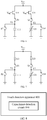
- FIGS. 2 to 4 are intended to help a person skilled in the art to better understand embodiments of the present application, and are not intended to limit the scope of the embodiments of the present application. Various equivalent modifications or variations based on FIGS. 2 to 4 also fall within the scope of the embodiments of the present application.
- the capacitance detection circuit 100 includes a first charging and discharging circuit 110, and the first charging and discharging circuit 110 includes a first current source 112, a first switch S1 and a second switch S2.
- a first end of the first current source 112 is connected to a power supply V DD
- a second end of the current source 112 is connected to a first end of a capacitor to be detected 111 through S1
- a second end of the capacitor to be detected 111 is grounded
- the first end of the capacitor to be detected 111 is also grounded through S2.
- S1 is configured to control a process in which the first current source 112 charges the capacitor to be detected 111
- S2 is configured to control a process in which the capacitor to be detected 111 discharges to the ground.
- the capacitance detection circuit 100 further includes a second charging and discharging circuit 120, and the second charging and discharging circuit 120 includes a second current source 122, a third switch S3 and a fourth switch S4.
- a first end of the second current source 122 is connected to a power supply V DD
- a second end of the first current source 112 is connected to a first end of a calibration capacitor 121 through S3
- a second end of the calibration capacitor 121 is grounded
- the first end of the calibration capacitor 121 is also grounded through S4.
- S3 is configured to control a process in which the first current source 112 charges the calibration capacitor 121
- S4 is configured to control a process in which the calibration capacitor 121 discharges to the ground.
- the first current source 112 and the second current source 122 may be proportional current sources, and a ratio between a current value I 1 of the first current source 112 and a current value I 2 of the second current source 122 may be fixed or adjustable.
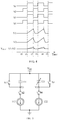
- a timing diagram shown in FIG. 4 in an initialization phase (a time period tO-tl), S2 and S4 are turned on, and S1 and S3 are turned off, so that the capacitor to be detected 111 and the calibration capacitor 121 are discharged, for example, completely discharged or discharged to a certain extent.
- the quantity of charges stored in the capacitor to be detected 111 and the calibration capacitor 121 are both 0, a voltage V1 of the capacitor to be detected 111 is equal to 0, a voltage V2 of the calibration capacitor 121 is equal to 0, and a voltage difference between them is 0.
- FIG. 4 shows a changing rule of the voltage V1 of the capacitor to be detected 111 and a changing rule of the voltage V2 of the calibration capacitor 121 in the charging phase.
- FIG. 4 shows a changing rule of the voltage V1 of the capacitor to be detected 111 and a changing rule of the voltage V2 of the calibration capacitor 121 in the discharging phase.
- a ratio between a current value I 1 of the first current source 112 and a current value I 2 of the second current source 122, and a capacitance Cc of the calibration capacitor 121 are adjusted so that C C ⁇ C X ⁇ I 2 /I 1 , where Cx is a capacitance of the capacitor to be detected 111.
- the capacitance value Cx of the capacitor to be detected 111 is approximately equal to Co, i.e., C X ⁇ C 0 , then V1 ⁇ V2, and a voltage difference between V1 and V2 is always close to 0, as shown by the dotted line corresponding to V OUT in FIG. 4 .
- the capacitance Cx of the capacitor to be detected 111 is approximately equal to C 0 + ⁇ C, i.e., C X ⁇ C 0 + ⁇ C, and an increasing rate of V1 in the charging process decreases, then V1 ⁇ V2 in the charging phase, therefore the voltage difference between V1 and V2 also increases, and a changing rule of the voltage difference is shown by the solid line corresponding to V OUT in FIG. 4 .
- the values of Cc and I 2 /I 1 may be set, so that the energy value of the fundamental frequency of the voltage difference between the capacitor to be detected 111 and the calibration capacitor 121 is as small as possible, for example, less than a predetermined value, when no touch occurs.
- the energy value of the fundamental frequency when no touch occurs may be denoted as A1, which may be used as a reference for determining whether the energy value changes in the subsequent.
- the value of Cc may be set, so that the difference value between Cc and C 0 ⁇ I 2 /I 1 is less than a preset value, that is, it is considered that the detection requirement may be satisfied.
- a time period t1-t3 is a charging and discharging period, and when the capacitance detection is performed once, data in one or more charging and discharging periods may be collected, that is, corresponding operations in the time period t1-t3 may be performed one or more times, and the capacitance variation of the capacitor to be detected 111 may be detected according to the change of the difference value between the voltage signal between the capacitor to be detected 111 and the calibration capacitor 121 in these charging and discharging periods.
- the solid line corresponding to V OUT in the last row in FIG. 4 may be approximately regarded as a periodic triangular wave.
- the periodic triangular wave signal is continuously sampled, and the energy value of the fundamental frequency of the difference value between the voltage signals of the capacitor to be detected 111 and the calibration capacitor 121 may be obtained according to the sampled data.
- the capacitance detection circuit 100 further includes an instrumentation operational amplifier IA 150, a filter 160, an analog-to-digital conversion circuit 130 and a digital processing circuit 140.
- IA 150 an instrumentation operational amplifier
- a filter 160 an analog-to-digital conversion circuit 130
- a digital processing circuit 140 Two input ends of IA 150 respectively receive voltage signals of the capacitor to be detected 111 and the calibration capacitor 121, and amplify and output a difference value between the voltage signals of the capacitor to be detected 111 and the calibration capacitor 121, where the output signal V OUT is equal to
- , i.e., V OUT
- V OUT is output by IA 150 to the filter 160 for filtering, and the filtered voltage signal V OUT is input to ADC 130.
- the ADC 130 continuously samples the voltage signal V OUT , that is, continuously samples the periodic triangular wave curve in FIG. 4 .
- a sampled frequency of ADC 130 shall not be too small, and preferably, the sampled frequency thereof may be greater than or equal to twice the signal bandwidth.
- a sampled interval is Ts, that is, the ADC 130 samples a point every T S .
- Voltage data of the 2 M sampled points sampled by the ADC 130 is transmitted to the digital processing circuit 140, and the digital processing circuit 140 processes these sampled points to obtain the energy value of the fundamental frequency of the sampled data of the periodic triangular wave curve in FIG. 4 .
- the fundamental frequency is, for example, 1/T C
- the energy value may be understood as a magnitude of signal amplitude of the fundamental frequency. That is, the digital processing circuit 140 determines the magnitude of the amplitude at the 1/T C frequency point in a frequency spectrum according to the data collected by the analog-to-digital conversion circuit 130, thereby determining the capacitance of the capacitor to be detected 111.
- the voltage signal is digitally demodulated after analog-to-digital conversion is performed, so as to detect the capacitance variation of the capacitor to be detected in a digital domain. Since the interference signal and the useful signal have different frequencies, detecting the capacitance variation of the capacitor to be detected in the digital domain could reduce the noise interference, improve the signal-to-noise ratio of the capacitance detection circuit and improve the detection performance of the capacitance detection circuit.
- the embodiment of the present application does not limit the structure of the data processing circuit, as long as the energy value of the fundamental frequency of the sampled signal can be obtained.
- the data processing circuit 140 may include a digital demodulator.
- the digital demodulator may perform digital quadrature demodulation on the sampled data to obtain the energy value of the fundamental frequency.
- the digital demodulator may perform Fourier transform (Fast Fourier Transform, FFT) on the sampled data to obtain a spectrogram, and obtain the energy value of the fundamental frequency according to the spectrogram.
- FFT Fast Fourier Transform
- the digital demodulator may also obtain the energy value of the fundamental frequency in other ways, which is not limited here.
- the digital processing unit 140 determines the variation of the capacitance Cx of the capacitor to be detected 111 according to the energy value of the fundamental frequency of the voltage difference between the capacitor to be detected 111 and the calibration capacitor 112 in the charging or discharging process. For example, when an energy value A2 of the fundamental frequency of the voltage difference is less than a preset threshold value, it may be considered that the capacitance Cx has not changed, and at this time, a differential output V OUT of IA 150 is equal to
- the energy value of the fundamental frequency is A1 when there is no touch and the energy value of the fundamental frequency is A2 when there is a touch
- the operation of touching here may be understood as operation such as contacting, approaching, pressing, or the like.
- the capacitor to be detected 111 and the calibration capacitor 121 in FIG. 2 may also be charged by a power supply, and the capacitor to be detected 111 and the calibration capacitor 121 are driven by the first current source 112 and the second current source 122 to discharge.
- one end of the capacitor to be detected 111 and the calibration capacitor 121 is connected to a power supply, and the other end thereof is connected to a current source, and the other end of the current source is grounded.
- S1 and S3 are turned on, S2 and S4 are turned off, and the capacitor to be detected 111 and the calibration capacitor 121 are charged by a power supply V DD .
- the current sources are used to drive charging or discharging of the capacitor to be detected 111 and the calibration capacitor 121
- other devices such as a voltage source, may also be used to perform charging or discharging on the capacitor to be detected 111 and the calibration capacitor 121.
- the first charging and discharging circuit 110 and the second charging and discharging circuit 120 may adopt the same or different types of devices to perform charging or discharging on the capacitor to be detected 111 and the calibration capacitor 121, which is not limited in the present application.
- the first current source 112 shown in FIG. 2 may be replaced by a first resistor 113 or a first transistor 113
- the second current source 122 may be replaced by a second resistor 123 or a second transistor 124.
- the corresponding technical features may be referred to the foregoing description about FIGS. 2 to 4 , which is not repeatedly described here for brevity.
- the first transistor 114 and the second transistor 124 charge the capacitor to be detected 111 and the calibration capacitor 121, respectively, while in a time period t2-t3, the capacitor to be detected 111 and the calibration capacitor 121 are discharged to the ground, thereby realizing the capacitance detection of the capacitor to be detected 111.
- the first resistor 113 and the second resistor 123 charge the capacitor to be detected 111 and the calibration capacitor 121, respectively, while in a time period t2-t3, the capacitor to be detected 111 and the calibration capacitor 121 are discharged to the ground, thereby realizing the capacitance detection of the capacitor to be detected 111.
- the capacitance detection circuit 100 of an embodiment of the present application may be applied to various touch control devices.
- the capacitor to be detected 111 may be a capacitive sensor disposed on a touch control panel, and the capacitive sensor is configured to detect touch information of a finger on the touch control panel, such as touch position, touch pressure and other information.
- FIG. 8 is a schematic block diagram of a touch detection apparatus 800 according to an embodiment of the present application.
- the touch detection apparatus 800 may include the capacitance detection circuit 100 shown in FIG. 1 .
- the touch detection apparatus 800 may further determine touch information of a user according to the capacitance of the capacitor to be detected 111 determined by the capacitance detection circuit 100.
- the touch detection apparatus 800 determines the touch information of the user according to a capacitance variation ⁇ C of the capacitor to be detected 111 determined by the capacitance detection circuit 100 relative to a base capacitance Co.
- An embodiment of the present application also provides an electronic device 900, and as shown in FIG. 9 , the electronic device 900 includes the touch detection apparatus 800 shown in FIG. 8 .
- the electronic device in the embodiment of the present application may be portable or mobile computing devices such as a terminal device, a mobile phone, a tablet computer, a notebook computer, a desktop computer, a gaming device, an in-vehicle electronic device or a wearable smart device, and other electronic devices such as an electronic database, an automobile and an automated teller machine (ATM).
- the wearable intelligent device includes a device, such as a smart watch or smart glasses, that is of a full function and a large size and that can implement all or some functions without relying on a smartphone, and a device, such as a smart band or smart jewelry that performs sign monitoring, that is dedicated to only one type of application function and that needs to be used together with another device such as a smartphone.
Landscapes
- Engineering & Computer Science (AREA)
- Physics & Mathematics (AREA)
- General Physics & Mathematics (AREA)
- General Engineering & Computer Science (AREA)
- Theoretical Computer Science (AREA)
- Human Computer Interaction (AREA)
- Measurement Of Resistance Or Impedance (AREA)
Abstract
Description
- The present application relates to the field of integrated circuits, in particular, to a capacitance detection circuit, a touch detection apparatus and an electronic device.
- Capacitive sensors are widely used in the field of human-machine interaction of electronic products. Specifically, a capacitor is formed between a detection electrode and ground, when a conductor (such as a finger) approaches or touches the detection electrode, a capacitance between the detection electrode and the ground changes. By detecting a variation of the capacitance, information that the conductor approaches or touches the detection electrode is acquired, so as to determine user operation. The performance of a capacitance detection circuit has a direct impact on user operation experience, and therefore, it is urgent to solve a problem of how to improve detection performance of the capacitance detection circuit.
- Embodiments of the present application provide a capacitance detection circuit, a touch detection apparatus and an electronic device, and the capacitance detection circuit has better detection performance.
- According to a first aspect, provided is a capacitance detection circuit, including: a first charging and discharging circuit, configured to perform charging or discharging on a capacitor to be detected; a second charging and discharging circuit, configured to perform charging or discharging on a calibration capacitor; an analog-to-digital conversion circuit, configured to continuously sample a voltage difference between the capacitor to be detected and the calibration capacitor in a charging or discharging process to obtain sampled data; and a digital processing circuit, configured to detect a capacitance of the capacitor to be detected according to the sampled data.
- In one possible implementation manner, the digital processing circuit is configured to detect the capacitance of the capacitor to be detected according to an energy value of a fundamental frequency of the sampled data.
- In one possible implementation manner, the digital processing circuit includes a digital demodulator, where the digital demodulator is configured to perform digital quadrature demodulation or Fourier transform on the sampled data to obtain the energy value of the fundamental frequency.
- In one possible implementation manner, each charging and discharging period includes a charging phase and a discharging phase; in the charging phase, the first charging and discharging circuit and the second charging and discharging circuit are respectively configured to simultaneously charge the capacitor to be detected and the calibration capacitor; and in the discharging phase, the first charging and discharging circuit and the second charging and discharging circuit are respectively configured to simultaneously perform discharging on the capacitor to be detected and the calibration capacitor.
- In one possible implementation manner, the first charging and discharging circuit includes a first current source configured to perform charging or discharging on the capacitor to be detected; and the second charging and discharging circuit includes a second current source configured to perform charging or discharging on the calibration capacitor.
- In one possible implementation manner, a first end of the first current source is connected to a power supply, a second end of the first current source is connected to a first end of the capacitor to be detected through a first switch, the first end of the capacitor to be detected is also grounded through a second switch, and a second end of the capacitor to be detected is grounded; and a first end of the second current source is connected to the power supply, a second end of the second current source is connected to a first end of the calibration capacitor through a third switch, the first end of the calibration capacitor is also grounded through a fourth switch, and a second end of the calibration capacitor is grounded.
- In one possible implementation manner, a first end of the first current source is grounded, a second end of the first current source is connected to a first end of the capacitor to be detected through a first switch, the first end of the capacitor to be detected is also connected to a power supply through a second switch, and a second end of the capacitor to be detected is grounded; and a first end of the second current source is grounded, and a second end of the second current source is connected to a first end of the calibration capacitor through a third switch, the first end of the calibration capacitor is also connected to the power supply through a fourth switch, and a second end of the calibration capacitor is grounded.
- In one possible implementation manner, Cc is equal to CX×I2/I1, or a difference value between Cc and C0×I2/I1 is less than a preset value, where Co is a base capacitance of the capacitor to be detected, Cc is a capacitance of the calibration capacitor, I1 is a current value of the first current source, and I2 is a current value of the second current source.
- In one possible implementation manner, the first charging and discharging circuit includes a first resistor configured to perform charging or discharging on the capacitor to be detected; and the second charging and discharging circuit includes a second resistor configured to perform charging or discharging on the calibration capacitor.
- In one possible implementation manner, a first end of the first resistor is connected to a power supply, a second end of the first resistor is connected to a first end of the capacitor to be detected through the first switch, the first end of the capacitor to be detected is also grounded through the second switch, and a second end of the capacitor to be detected is grounded; and a first end of the second resistor is connected to the power supply, a second end of the second resistor is connected to a first end of the calibration capacitor through the third switch, the first end of the calibration capacitor is also grounded through the fourth switch, and a second end of the calibration capacitor is grounded.
- In one possible implementation manner, a first end of the first resistor is grounded, a second end of the first resistor is connected to a first end of the capacitor to be detected through a first switch, the first end of the capacitor to be detected is also connected to a power supply through a second switch, and a second end of the capacitor to be detected is grounded; and a first end of the second resistor is grounded, and a second end of the second resistor is connected to a first end of the calibration capacitor through a third switch, the first end of the calibration capacitor is also connected to the power supply through a fourth switch, and a second end of the calibration capacitor is grounded.
- In one possible implementation manner, the first charging and discharging circuit includes a first transistor configured to perform charging or discharging on the capacitor to be detected; and the second charging and discharging circuit includes a second transistor configured to perform charging or discharging on the calibration capacitor.
- In one possible implementation manner, the first transistor and the second transistor are N-type metal-oxide semiconductor (MOS) transistors, a gate of the first transistor is connected to a fixed level, a drain of the first transistor is connected to a power supply, a source of the first transistor is connected to a first end of the capacitor to be detected through a first switch, the first end of the capacitor to be detected is also grounded through a second switch, and a second end of the capacitor to be detected is grounded; and a gate of the second transistor is connected to a fixed level, a drain of the second transistor is connected to the power supply, a source of the second transistor is connected to a first end of the calibration capacitor through a third switch, the first end of the calibration capacitor is also grounded through a fourth switch, and a second end of the calibration capacitor is grounded.
- In one possible implementation manner, the first transistor and the second transistor are P-type MOS transistors, a gate of the first transistor is connected to a fixed level, a drain of the first transistor is grounded, a source of the first transistor is connected to a first end of the capacitor to be detected through a first switch, the first end of the capacitor to be detected is connected to a power supply through a second switch, and a second end of the capacitor to be detected is connected to the power supply; and a gate of the second transistor is connected to a fixed level, a drain of the second transistor is grounded, a source of the second transistor is connected to a first end of the calibration capacitor through a third switch, the first end of the calibration capacitor is also connected to the power supply through a fourth switch, and a second end of the calibration capacitor is connected to the power supply.
- In one possible implementation manner, the capacitance detection circuit further includes a control circuit, configured to in the charging phase, control the second switch and the fourth switch to be turned on, and control the first switch and the third switch to be turned off; in the discharging phase, control the first switch and the third switch to be turned on, and control the second switch and the fourth switch to be turned off.
- In one possible implementation manner, TC=2M×TS, where TC is a length of N charging and discharging period(s), 2M is the number of sampled points in the N charging and discharging period(s), Ts is a time interval between two adjacent sampled points, and M and N are positive integers.
- In one possible implementation manner, the fundamental frequency is 1/Tc.
- In one possible implementation manner, the capacitance detection circuit further includes an operational amplifier, where two input ends of the operational amplifier are respectively connected to the capacitor to be detected and the calibration capacitor.
- In one possible implementation manner, the operational amplifier is a continuous instrumentation operational amplifier.
- In one possible implementation manner, the capacitance detection circuit further includes a filter, where an input end of the filter is connected to an output end of the operational amplifier, and an output end of the filter is connected to an input end of the analog-to-digital conversion circuit.
- In one possible implementation manner, the capacitor to be detected is a capacitive sensor disposed on a touch control panel, and the capacitive sensor is configured to detect touch information of a finger on the touch control panel.
- In one possible implementation manner, when the energy value of the fundamental frequency is less than a threshold value, it indicates that no finger touches the capacitive sensor; and when the energy value of the fundamental frequency is greater than the threshold value, it indicates that a finger touches the capacitive sensor.
- According to a second aspect, an embodiment of the present application provides a touch detection apparatus, including the capacitance detection circuit in the first aspect or any one of possible implementation manners of the first aspect.
- According to a third aspect, an embodiment of the present application provides an electronic device, including the touch detection apparatus according to the second aspect.
- Based on the foregoing technical solution, an analog-to-digital conversion circuit may continuously sample a voltage difference between a capacitor to be detected and a calibration capacitor in a charging or discharging process, to obtain a change situation of the voltage difference in the charging or discharging process; and a digital processing circuit may detect a capacitance variation of the capacitor to be detected by processing the continuously sampled data. Since the sampled data is obtained by continuously sampling the voltage difference, the sampled data is associated with the voltage difference, so that the capacitance of the capacitor to be detected may be detected according to the sampled data. Because the capacitance variation of the capacitor to be detected is detected in a digital domain and an interference signal and a useful signal have different frequencies, noise interference could be reduced and a signal-to-noise ratio of the capacitance detection circuit could be improved.
-
-
FIG. 1 is a schematic block diagram of a conventional capacitance detection circuit. -
FIG. 2 is a possible schematic structural diagram of the capacitance detection circuit shown inFIG. 1 . -
FIG. 3 is a possible schematic structural diagram of the capacitance detection circuit shown inFIG. 1 . -
FIG. 4 is a timing diagram corresponding to the capacitance detection circuit shown inFIG. 2 . -
FIG. 5 is another possible schematic structural diagram of the capacitance detection circuit shown inFIG. 1 . -
FIG. 6 is another possible schematic structural diagram of the capacitance detection circuit shown inFIG. 1 . -
FIG. 7 is another possible schematic structural diagram of the capacitance detection circuit shown inFIG. 1 . -
FIG. 8 is a schematic block diagram of atouch detection apparatus 800 according to an embodiment of the present application. -
FIG. 9 is a schematic block diagram of anelectronic device 900 according to an embodiment of the present application. - Embodiments of the present application will be described hereinafter in conjunction with the drawings in the embodiments of the present application.
- A capacitive sensor is widely used in a plurality of electronic systems, and is usually used as an input device of a system to provide input information, such as position, motion, force and duration. Generally, a user operates such as approaching, touching, pressing or sliding, one or more sensing areas of a capacitive sensor, to generate a capacitive effect with the sensing areas, and a user operation may be determined by quantifying the capacitive effect.
-
FIG. 1 is a schematic structural diagram of acapacitance detection circuit 100 according to an embodiment of the present application. As shown inFIG. 1 , thecapacitance detection circuit 100 is connected to a capacitor to be detected 111, and thecapacitance detection circuit 100 includes: - a first charging and discharging
circuit 110, configured to perform charging or discharging on the capacitor to be detected 111; - a second charging and discharging
circuit 120, configured to perform charging or discharging on acalibration capacitor 121; - an analog-to-
digital conversion circuit 130, configured to continuously sample a voltage difference between the capacitor to be detected 111 and thecalibration capacitor 121 in a charging or discharging process to obtain sampled data; and - a
digital processing circuit 140, configured to detect a capacitance of the capacitor to be detected 111 according to the sampled data. - In this embodiment, the analog-to-
digital conversion circuit 130 may continuously sample the voltage difference between the capacitor to be detected 111 and thecalibration capacitor 121 in the charging or discharging process, to obtain a change situation of the voltage difference in the charging or discharging process; and thedigital processing circuit 140 may detect a capacitance variation of the capacitor to be detected by processing the continuously sampled data. Since the sampled data is obtained by continuously sampling the voltage difference, an energy value of a fundamental frequency of the sampled data is associated with the voltage difference, so that the capacitance of the capacitor to be detected may be detected according to the energy value of the fundamental frequency. Because the capacitance variation of the capacitor to be detected is detected in a digital domain and an interference signal and a useful signal have different frequencies, noise interference could be reduced and a signal-to-noise ratio of the capacitance detection circuit could be improved. - The
capacitance detection circuit 100 in this embodiment may be applied to, for example, a capacitive sensor, where the capacitor to be detected 111 is a sensing-capacitor of the capacitive sensor. - When there is no touch, a capacitance Cx of the capacitor to be detected 111 is equal to a base capacitance Co.
- When there is a touch, a capacitance Cx of the capacitor to be detected 111 is increased by ΔC to be CX=C0+ΔC.
- The
calibration capacitor 121 may be, for example, a variable capacitor array or a fixed capacitor. - The first charging and discharging
circuit 110 may include devices such as, a current source, a resistor, a transistor, or the like, configured to perform charging or discharging on the capacitor to be detected 111. - The second charging and
discharging circuit 120 may include devices such as, a current source, a resistor, a transistor, or the like, configured to perform charging or discharging on thecalibration capacitor 121. - In a process of performing charging or discharging on the capacitor to be detected 111 and the
calibration capacitor 121, a voltage of the capacitor to be detected 111 and a voltage of thecalibration capacitor 121 change according to a certain rule, and a voltage difference between the capacitor to be detected 111 and thecalibration capacitor 121 also changes according to a certain rule. After the analog-to-digital conversion circuit 130 continuously samples the voltage difference that continuously changes in the charging or discharging process, thedigital processing circuit 140 may obtain capacitance information of the capacitor to be detected 111 from the sampled data. - For example, the digital processing circuit is configured to detect the capacitance of the capacitor to be detected according to the energy value of the fundamental frequency of the sampled data. The energy value of the fundamental frequency of the sampled data reflects a change situation of the voltage difference. The larger the energy value of the fundamental frequency is, it indicates that the larger the voltage difference is, and therefore the larger a capacitance variation of the capacitor to be detected 111 is. On the contrary, the smaller the energy value of the fundamental frequency is, it indicates that the smaller the voltage difference is, and therefore the larger a capacitance variation of the capacitor to be detected 111 is.
- The analog-to-
digital conversion circuit 130 may sample a voltage difference between the capacitor to be detected 111 and thecalibration capacitor 121 in N charging and discharging period(s) each time, where N is a positive integer. Optionally, each charging and discharging period includes a charging phase and a discharging phase. - In the charging phase, the first charging and discharging
circuit 110 and the second charging and dischargingcircuit 120 are respectively configured to simultaneously charge the capacitor to be detected 111 and thecalibration capacitor 121. In the discharging phase, the first charging and dischargingcircuit 110 and the second charging and dischargingcircuit 120 are respectively configured to simultaneously perform discharging on the capacitor to be detected 111 and thecalibration capacitor 121. - The N charging and discharging period(s) constitutes a driving period, and during the driving period, the analog-to-
digital conversion circuit 130 continuously samples the voltage difference between the capacitor to be detected 111 and thecalibration capacitor 121, and transmits sampled data to thedigital processing circuit 140. Since a change rule of the voltage difference in each charging and discharging period is the same, in the N charging and discharging period(s) the voltage difference periodically changes. Thedigital processing circuit 140 demodulates the received sampled data that is periodically distributed and obtains the energy value of the fundamental frequency of the sampled data, thereby determining the capacitance of the capacitor to be detected 111 according to the energy value. - It should be understood that in the embodiment of the present application, a charging and discharging circuit charging a capacitor refers to a process in which charges are transferred to the capacitor to increase the quantity of charges stored in the capacitor, and a charging and discharging circuit performing discharging on a capacitor refers to a process in which charges are transferred from the capacitor to reduce the quantity of charges stored in the capacitor.
- The embodiment of the present application does not limit the implementation forms of the first charging and discharging
circuit 110 and the second charging and dischargingcircuit 120. As an example, the present application provides the following three implementation manners. - The first charging and discharging
circuit 110 includes a firstcurrent source 112, and the second charging and dischargingcircuit 120 includes a secondcurrent source 122. - Optionally, the first
current source 112 is configured to charge the capacitor to be detected 111, and the secondcurrent source 122 is configured to charge thecalibration capacitor 121. - For example, a first end of the first
current source 112 is connected to a power supply VDD, and a second end of the firstcurrent source 112 is connected to a first end of the capacitor to be detected 111 through a first switch S1, the first end of the capacitor to be detected 111 is also grounded through a second switch S2, and a second end of the capacitor to be detected 111 is grounded; and a first end of the secondcurrent source 122 is connected to the power supply VDD, and a second end of the secondcurrent source 122 is connected to a first end of thecalibration capacitor 121 through a third switch S3, the first end of thecalibration capacitor 121 is also grounded through a fourth switch S4, and a second end of thecalibration capacitor 121 is grounded. - Optionally, the first
current source 112 is configured to perform discharging on the capacitor to be detected 111, and the secondcurrent source 122 is configured to perform discharging on thecalibration capacitor 121. - For example, a first end of the first
current source 112 is grounded, and a second end of the firstcurrent source 112 is connected to a first end of the capacitor to be detected 111 through a first switch S1, the first end of the capacitor to be detected 111 is also connected to a power supply VDD through a second switch S2, and a second end of the capacitor to be detected 111 is grounded; and a first end of the secondcurrent source 122 is grounded, and a second end of the secondcurrent source 122 is connected to a first end of thecalibration capacitor 121 through a third switch S3, the first end of thecalibration capacitor 121 is also connected to the power supply VDD through a fourth switch S4, and a second end of thecalibration capacitor 121 is grounded. - Optionally, it may be set that CC=C0×I2/I1, where Co is a base capacitance of the capacitor to be detected 111, Cc is a capacitance of the
calibration capacitor 121, I1 is a current value of the firstcurrent source 112, and I2 is a current value of the secondcurrent source 122. - At this time, the voltage difference between the capacitor to be detected 111 and the
calibration capacitor 121 reflects a capacitance variation ΔC of the capacitor to be detected 111 relative to the base capacitance Co, and is independent of Co. Therefore, the base capacitance Co is cancelled in a voltage domain, so that thecapacitance detection circuit 100 is no longer affected by the base capacitance Co, and the detection sensitivity and accuracy of thecapacitance detection circuit 100 are improved. - If the cancellation of the base capacitance Co is not considered, the capacitance of the
calibration capacitor 121 may be reduced by setting CC<C0 × I2/I1, thereby reducing a volume of thecapacitance detection circuit 100 and the cost of a chip. - It should be understood that when the
capacitance detection circuit 100 is applied to touch detection, the base capacitance Co may be considered as a capacitance of the capacitor to be detected 111 to the ground when there is no touch. When there is a touch, the capacitance of the capacitor to be detected 111 is increased by ΔC relative to the base capacitance Co, and ΔC reflects touch information of the user. - The first charging and discharging
circuit 110 includes afirst resistor 113, and the second charging and dischargingcircuit 120 includes a second resistor 123. - Optionally, the
first resistor 113 is configured to charge the capacitor to be detected 111, and the second resistor 123 is configured to charge thecalibration capacitor 121. - For example, a first end of the
first resistor 113 is connected to a power supply VDD, and a second end of thefirst resistor 113 is connected to a first end of the capacitor to be detected 111 through a first switch S1, the first end of the capacitor to be detected 111 is also grounded through a second switch S2, and a second end of the capacitor to be detected 111 is grounded; and a first end of the second resistor 123 is connected to the power supply VDD, and a second end of the second resistor 123 is connected to a first end of thecalibration capacitor 121 through a third switch S3, the first end of thecalibration capacitor 121 is also grounded through a fourth switch S4, and a second end of thecalibration capacitor 121 is grounded. - Optionally, the
first resistor 113 is configured to perform discharging on the capacitor to be detected 111, and the second resistor 123 is configured to perform discharging on thecalibration capacitor 121. - For example, a first end of the
first resistor 113 is grounded, and a second end of thefirst resistor 113 is connected to a first end of the capacitor to be detected 111 through a first switch S1, the first end of the capacitor to be detected 111 is also connected to a power supply VDD through a second switch S2, and a second end of the capacitor to be detected 111 is grounded; and a first end of the second resistor 123 is grounded, and a second end of the second resistor 123 is connected to a first end of thecalibration capacitor 121 through a third switch S3, the first end of thecalibration capacitor 121 is also connected to the power supply VDD through a fourth switch S4, and a second end of thecalibration capacitor 121 is grounded. - The first charging and discharging
circuit 110 includes afirst transistor 114, and the second charging and dischargingcircuit 120 includes asecond transistor 124. - The
first transistor 114 and thesecond transistor 124 may be, for example, an N-type metal-oxide semiconductor (Metal-Oxide Semiconductor, MOS) transistor or a P-type MOS transistor. - Optionally, the
first transistor 114 is configured to charge the capacitor to be detected 111, and thesecond transistor 124 is configured to charge thecalibration capacitor 121. - For example, a gate (Gate, G for short) of the
first transistor 114 is connected to a level Vbn, and the level Vbn makes thefirst transistor 114 work in a saturation region, a drain (Drain, D for short) of thefirst transistor 114 is connected to a power supply VDD, and a source (Source, S for short) of thefirst transistor 114 is connected to a first end of the capacitor to be detected 111 through a first switch S1, the first end of the capacitor to be detected 111 is also grounded through a second switch S2, and a second end of the capacitor to be detected 111 is grounded; and a gate G of thesecond transistor 124 is connected to a level Vbn, and the level Vbn makes thesecond transistor 124 work in a saturation region, a drain D of thesecond transistor 124 is connected to a power supply VDD, a source S of thesecond transistor 124 is connected to a first end of thecalibration capacitor 121 through a third switch S3, the first end of thecalibration capacitor 121 is also grounded through a fourth switch S4, and a second end of thecalibration capacitor 121 is grounded. - Optionally, the
first transistor 114 is configured to perform discharging on the capacitor to be detected 111, and thesecond transistor 124 is configured to perform discharging on thecalibration capacitor 121. - For example, a gate G of the
first transistor 114 is connected to a fixed level Vbn, and the level Vbn makes thefirst transistor 114 work in a saturation region, a drain D of thefirst transistor 114 is grounded, a source S of thefirst transistor 114 is connected to a first end of the capacitor to be detected 111 through a first switch S1, the first end of the capacitor to be detected 111 is also connected to a power supply VDD through a second switch S2, and a second end of the capacitor to be detected 111 is connected to the power supply VDD; and a gate G of thesecond transistor 124 is connected to a fixed level Vbn, and the level Vbn makes thesecond transistor 124 work in a saturation region, a drain D of thesecond transistor 124 is grounded, a source S of thesecond transistor 124 is connected to a first end of thecalibration capacitor 121 through a third switch S3, the first end of thecalibration capacitor 121 is also connected to a power supply VDD through a fourth switch S4, and a second end of thecalibration capacitor 121 is connected to the power supply VDD. - In one implementation manner, the
capacitance detection circuit 100 further includes a control circuit configured to control the foregoing switches and related circuits to perform corresponding operations. - For example, in a charging phase, the control circuit controls the second switch S2 and the fourth switch S4 to be turned on, and controls the first switch S1 and the third switch S3 to be turned on, so that the first charging and discharging
circuit 110 and the second charging and dischargingcircuit 120 respectively charge the capacitor to be detected 111 and thecalibration capacitor 121 simultaneously. In a discharging phase, the control circuit controls the first switch S1 and the third switch S3 to be turned on, and controls the second switch S2 and the fourth switch S4 to be turned off, so that the capacitor to be detected 111 and thecalibration capacitor 121 are discharged simultaneously. - In one implementation manner, the
capacitance detection circuit 100 further includes anoperational amplifier 150, where two input ends of theoperational amplifier 150 are respectively connected to the capacitor to be detected 111 and thecalibration capacitor 121. - For example, one input end of an
IA 150 inFIG. 3 may be connected to the first end of the capacitor to be detected 111 inFIG. 2 , and the other input end of theIA 150 is connected to the first end of thecalibration capacitor 121 inFIG. 2 . Since adigital processing unit 140 needs to sample a continuous voltage signal, preferably, theoperational amplifier 150 is a continuous operational amplifier, such as an instrumentation operational amplifier (Instrumentation Amplifier, IA or INA), so as to amplify the continuous voltage signal. - In one implementation manner, the
capacitance detection circuit 100 further includes afilter 160. An input end of thefilter 160 is connected to an output end of theoperational amplifier 150, and an output end of thefilter 160 is connected to an input end of an analog-to-digital conversion circuit 130. - The
filter 160 may be, for example, an anti-aliasing filter configured to reduce an aliasing frequency component in an output level. - Hereinafter, by taking a first
current source 112 and a secondcurrent source 122 as an example, a working process of acapacitance detection circuit 100 of the present application will be described in detail with reference toFIGS. 2 to 4 . - It should be understood that examples shown in
FIGS. 2 to 4 are intended to help a person skilled in the art to better understand embodiments of the present application, and are not intended to limit the scope of the embodiments of the present application. Various equivalent modifications or variations based onFIGS. 2 to 4 also fall within the scope of the embodiments of the present application. - As shown in
FIG. 2 , thecapacitance detection circuit 100 includes a first charging and dischargingcircuit 110, and the first charging and dischargingcircuit 110 includes a firstcurrent source 112, a first switch S1 and a second switch S2. A first end of the firstcurrent source 112 is connected to a power supply VDD, a second end of thecurrent source 112 is connected to a first end of a capacitor to be detected 111 through S1, a second end of the capacitor to be detected 111 is grounded, and the first end of the capacitor to be detected 111 is also grounded through S2. S1 is configured to control a process in which the firstcurrent source 112 charges the capacitor to be detected 111, and S2 is configured to control a process in which the capacitor to be detected 111 discharges to the ground. - The
capacitance detection circuit 100 further includes a second charging and dischargingcircuit 120, and the second charging and dischargingcircuit 120 includes a secondcurrent source 122, a third switch S3 and a fourth switch S4. A first end of the secondcurrent source 122 is connected to a power supply VDD, a second end of the firstcurrent source 112 is connected to a first end of acalibration capacitor 121 through S3, a second end of thecalibration capacitor 121 is grounded, and the first end of thecalibration capacitor 121 is also grounded through S4. S3 is configured to control a process in which the firstcurrent source 112 charges thecalibration capacitor 121, and S4 is configured to control a process in which thecalibration capacitor 121 discharges to the ground. - The first
current source 112 and the secondcurrent source 122 may be proportional current sources, and a ratio between a current value I1 of the firstcurrent source 112 and a current value I2 of the secondcurrent source 122 may be fixed or adjustable. - According to a timing diagram shown in
FIG. 4 , in an initialization phase (a time period tO-tl), S2 and S4 are turned on, and S1 and S3 are turned off, so that the capacitor to be detected 111 and thecalibration capacitor 121 are discharged, for example, completely discharged or discharged to a certain extent. At time t1, the quantity of charges stored in the capacitor to be detected 111 and thecalibration capacitor 121 are both 0, a voltage V1 of the capacitor to be detected 111 is equal to 0, a voltage V2 of thecalibration capacitor 121 is equal to 0, and a voltage difference between them is 0. - In a charging phase (a time period t1-t2), S1 and S3 are turned on, and S2 and S4 are turned off, so that the first
current source 112 charges the capacitor to be detected 111, for example, fully charged or charged to a certain extent, and the secondcurrent source 122 charges thecalibration capacitor 121, for example, fully charged or charged to a certain extent.FIG. 4 shows a changing rule of the voltage V1 of the capacitor to be detected 111 and a changing rule of the voltage V2 of thecalibration capacitor 121 in the charging phase. - In a discharging phase (a time period t2-t4), S2 and S4 are turned on, and S1 and S3 are turned off, so that the capacitor to be detected 111 and the
calibration capacitor 121 are discharged, for example, completely discharged or discharged to a certain extent.FIG. 4 shows a changing rule of the voltage V1 of the capacitor to be detected 111 and a changing rule of the voltage V2 of thecalibration capacitor 121 in the discharging phase. - A ratio between a current value I1 of the first
current source 112 and a current value I2 of the secondcurrent source 122, and a capacitance Cc of thecalibration capacitor 121 are adjusted so that CC≈CX×I2/I1, where Cx is a capacitance of the capacitor to be detected 111. At this time, if there is no touch, that is, the capacitance value Cx of the capacitor to be detected 111 is approximately equal to Co, i.e., CX≈C0, then V1≈V2, and a voltage difference between V1 and V2 is always close to 0, as shown by the dotted line corresponding to VOUT inFIG. 4 . When there is a touch, the capacitance Cx of the capacitor to be detected 111 is approximately equal to C0+ΔC, i.e., CX≈C0+ΔC, and an increasing rate of V1 in the charging process decreases, then V1<V2 in the charging phase, therefore the voltage difference between V1 and V2 also increases, and a changing rule of the voltage difference is shown by the solid line corresponding to VOUT inFIG. 4 . - In an ideal case, CC=C0 × I2/I1, and at this time, the voltage difference between V1 and V2 reflects the change of ΔC and is independent of C0, and therefore the base capacitance Co is cancelled in a voltage domain, so that the
capacitance detection circuit 100 is no longer affected by the base capacitance Co, and the detection sensitivity and accuracy of thecapacitance detection circuit 100 are improved. At this time, the dotted line corresponding to VOUT inFIG. 4 remains at 0. - In a practical application, since Cc may not be strictly equal to C0×I2/I1, the values of Cc and I2/I1 may be set, so that the energy value of the fundamental frequency of the voltage difference between the capacitor to be detected 111 and the
calibration capacitor 121 is as small as possible, for example, less than a predetermined value, when no touch occurs. At this time, the energy value of the fundamental frequency when no touch occurs may be denoted as A1, which may be used as a reference for determining whether the energy value changes in the subsequent. - In other words, the value of Cc may be set, so that the difference value between Cc and C0×I2/I1 is less than a preset value, that is, it is considered that the detection requirement may be satisfied.
- A time period t1-t3 is a charging and discharging period, and when the capacitance detection is performed once, data in one or more charging and discharging periods may be collected, that is, corresponding operations in the time period t1-t3 may be performed one or more times, and the capacitance variation of the capacitor to be detected 111 may be detected according to the change of the difference value between the voltage signal between the capacitor to be detected 111 and the
calibration capacitor 121 in these charging and discharging periods. When data in a plurality of charging and discharging periods are collected each time, the solid line corresponding to VOUT in the last row inFIG. 4 may be approximately regarded as a periodic triangular wave. The periodic triangular wave signal is continuously sampled, and the energy value of the fundamental frequency of the difference value between the voltage signals of the capacitor to be detected 111 and thecalibration capacitor 121 may be obtained according to the sampled data. - As shown in
FIG. 3 , thecapacitance detection circuit 100 further includes an instrumentationoperational amplifier IA 150, afilter 160, an analog-to-digital conversion circuit 130 and adigital processing circuit 140. Two input ends ofIA 150 respectively receive voltage signals of the capacitor to be detected 111 and thecalibration capacitor 121, and amplify and output a difference value between the voltage signals of the capacitor to be detected 111 and thecalibration capacitor 121, where the output signal VOUT is equal to |V1-V2|, i.e., VOUT=|V1-V2|. - Within N charging and discharging period(s), after V1 and V2 are input to
IA 150, VOUT is output byIA 150 to thefilter 160 for filtering, and the filtered voltage signal VOUT is input toADC 130. TheADC 130 continuously samples the voltage signal VOUT, that is, continuously samples the periodic triangular wave curve inFIG. 4 . - A sampled frequency of
ADC 130 shall not be too small, and preferably, the sampled frequency thereof may be greater than or equal to twice the signal bandwidth. - For example, a sampled interval is Ts, that is, the
ADC 130 samples a point every TS. A length of the N charging and discharging period(s) is TC, the number of sampled points in TC is 2M, M is a positive integer, and TC=2M×TS. - Voltage data of the 2M sampled points sampled by the
ADC 130 is transmitted to thedigital processing circuit 140, and thedigital processing circuit 140 processes these sampled points to obtain the energy value of the fundamental frequency of the sampled data of the periodic triangular wave curve inFIG. 4 . - The fundamental frequency is, for example, 1/TC, and the energy value may be understood as a magnitude of signal amplitude of the fundamental frequency. That is, the
digital processing circuit 140 determines the magnitude of the amplitude at the 1/TC frequency point in a frequency spectrum according to the data collected by the analog-to-digital conversion circuit 130, thereby determining the capacitance of the capacitor to be detected 111. - In an embodiment of the present application, the voltage signal is digitally demodulated after analog-to-digital conversion is performed, so as to detect the capacitance variation of the capacitor to be detected in a digital domain. Since the interference signal and the useful signal have different frequencies, detecting the capacitance variation of the capacitor to be detected in the digital domain could reduce the noise interference, improve the signal-to-noise ratio of the capacitance detection circuit and improve the detection performance of the capacitance detection circuit.
- It should be understood that the embodiment of the present application does not limit the structure of the data processing circuit, as long as the energy value of the fundamental frequency of the sampled signal can be obtained.
- Optionally, the
data processing circuit 140 may include a digital demodulator. - For example, the digital demodulator may perform digital quadrature demodulation on the sampled data to obtain the energy value of the fundamental frequency.
- For another example, the digital demodulator may perform Fourier transform (Fast Fourier Transform, FFT) on the sampled data to obtain a spectrogram, and obtain the energy value of the fundamental frequency according to the spectrogram.
- In addition, the digital demodulator may also obtain the energy value of the fundamental frequency in other ways, which is not limited here.
- The
digital processing unit 140 determines the variation of the capacitance Cx of the capacitor to be detected 111 according to the energy value of the fundamental frequency of the voltage difference between the capacitor to be detected 111 and thecalibration capacitor 112 in the charging or discharging process. For example, when an energy value A2 of the fundamental frequency of the voltage difference is less than a preset threshold value, it may be considered that the capacitance Cx has not changed, and at this time, a differential output VOUT ofIA 150 is equal to |V1-V2|, which is very small, CC≈CX×I2/I1, and V2≈V1, When the energy value A2 of the fundamental frequency of the voltage difference is greater than or equal to the threshold value, it may be considered that the capacitance Cx has changed, and at this time, the differential output VOUT ofIA 150 is equal to |V1-V2|, which is larger, and CC<CX×I2/I1, V2>V1. - If the energy value of the fundamental frequency is A1 when there is no touch and the energy value of the fundamental frequency is A2 when there is a touch, it may be determined whether the capacitance Cx changes according to a value of A2-A1. For example, if it is applied to touch detection, when A2-A1 is less than a preset threshold value, it may be considered that no touch has occurred; and when A2-A1 is greater than or equal to the preset threshold value, it may be considered that there is finger touch. The operation of touching here may be understood as operation such as contacting, approaching, pressing, or the like.
- The capacitor to be detected 111 and the
calibration capacitor 121 inFIG. 2 may also be charged by a power supply, and the capacitor to be detected 111 and thecalibration capacitor 121 are driven by the firstcurrent source 112 and the secondcurrent source 122 to discharge. For example, as shown inFIG. 5 , one end of the capacitor to be detected 111 and thecalibration capacitor 121 is connected to a power supply, and the other end thereof is connected to a current source, and the other end of the current source is grounded. At this time, in a time period t1-t2, S1 and S3 are turned on, S2 and S4 are turned off, and the capacitor to be detected 111 and thecalibration capacitor 121 are charged by a power supply VDD. In a time period t2-t3, S2 and S4 are turned on, S1 and S3 are turned off, and the capacitor to be detected 111 and thecalibration capacitor 121 are driven by the firstcurrent source 112 and the secondcurrent source 122 to discharge. In this way, the capacitance detection of the capacitor to be detected 111 may also be realized. - It should be understood that, expect that the current sources are used to drive charging or discharging of the capacitor to be detected 111 and the
calibration capacitor 121, other devices such as a voltage source, may also be used to perform charging or discharging on the capacitor to be detected 111 and thecalibration capacitor 121. In addition, the first charging and dischargingcircuit 110 and the second charging and dischargingcircuit 120 may adopt the same or different types of devices to perform charging or discharging on the capacitor to be detected 111 and thecalibration capacitor 121, which is not limited in the present application. For example, the firstcurrent source 112 shown inFIG. 2 may be replaced by afirst resistor 113 or afirst transistor 113, and the secondcurrent source 122 may be replaced by a second resistor 123 or asecond transistor 124. After replacement, the corresponding technical features may be referred to the foregoing description aboutFIGS. 2 to 4 , which is not repeatedly described here for brevity. - For example, taking
FIG. 6 as an example, in a time period t1-t2, thefirst transistor 114 and thesecond transistor 124 charge the capacitor to be detected 111 and thecalibration capacitor 121, respectively, while in a time period t2-t3, the capacitor to be detected 111 and thecalibration capacitor 121 are discharged to the ground, thereby realizing the capacitance detection of the capacitor to be detected 111. - For example, as shown in
FIG. 7 , in a time period t1-t2, thefirst resistor 113 and the second resistor 123 charge the capacitor to be detected 111 and thecalibration capacitor 121, respectively, while in a time period t2-t3, the capacitor to be detected 111 and thecalibration capacitor 121 are discharged to the ground, thereby realizing the capacitance detection of the capacitor to be detected 111. - The
capacitance detection circuit 100 of an embodiment of the present application may be applied to various touch control devices. For example, the capacitor to be detected 111 may be a capacitive sensor disposed on a touch control panel, and the capacitive sensor is configured to detect touch information of a finger on the touch control panel, such as touch position, touch pressure and other information. -
FIG. 8 is a schematic block diagram of atouch detection apparatus 800 according to an embodiment of the present application. As shown inFIG. 8 , thetouch detection apparatus 800 may include thecapacitance detection circuit 100 shown inFIG. 1 . Thetouch detection apparatus 800 may further determine touch information of a user according to the capacitance of the capacitor to be detected 111 determined by thecapacitance detection circuit 100. Specifically, thetouch detection apparatus 800 determines the touch information of the user according to a capacitance variation ΔC of the capacitor to be detected 111 determined by thecapacitance detection circuit 100 relative to a base capacitance Co. - An embodiment of the present application also provides an
electronic device 900, and as shown inFIG. 9 , theelectronic device 900 includes thetouch detection apparatus 800 shown inFIG. 8 . - By way of example but not limitation, the electronic device in the embodiment of the present application may be portable or mobile computing devices such as a terminal device, a mobile phone, a tablet computer, a notebook computer, a desktop computer, a gaming device, an in-vehicle electronic device or a wearable smart device, and other electronic devices such as an electronic database, an automobile and an automated teller machine (ATM). The wearable intelligent device includes a device, such as a smart watch or smart glasses, that is of a full function and a large size and that can implement all or some functions without relying on a smartphone, and a device, such as a smart band or smart jewelry that performs sign monitoring, that is dedicated to only one type of application function and that needs to be used together with another device such as a smartphone.
- It shall be noted that each embodiment described in the present application and/or the technical features in each embodiment can be combined with each other arbitrarily in the case of no conflict, and the technical solutions obtained after combination should also fall into the protection scope of the present application.
- It should be understood that the specific examples in the embodiments of the present application are only to help a person skilled in the art to better understand the embodiments of the present application, but not to limit the scope of the embodiments of the present application. Various modifications and variations which fall within the scope of the present application can be made by those skilled in the art based on the foregoing embodiments.
- The foregoing descriptions are merely specific implementation manners of the present application. However, the protection scope of the present application is not limited thereto, and a person skilled in the art who is familiar with the art could readily think of variations or substitutions within the technical scope disclosed by the present application, and these variations or substitutions shall fall within the protection scope of the present application. Therefore, the protection scope of the present application shall be subject to the protection scope of the claims.
Claims (24)
- A capacitance detection circuit, comprising:a first charging and discharging circuit, configured to perform charging or discharging on a capacitor to be detected;a second charging and discharging circuit, configured to perform charging or discharging on a calibration capacitor;an analog-to-digital conversion circuit, configured to continuously sample a voltage difference between the capacitor to be detected and the calibration capacitor in a charging or discharging process to obtain sampled data; anda digital processing circuit, configured to detect a capacitance of the capacitor to be detected according to the sampled data.
- The capacitance detection circuit according to claim 1, wherein the digital processing circuit is configured to detect the capacitance of the capacitor to be detected according to an energy value of a fundamental frequency of the sampled data.
- The capacitance detection circuit according to claim 2, wherein the digital processing circuit comprises a digital demodulator, wherein the digital demodulator is configured to perform digital quadrature demodulation or Fourier transform on the sampled data to obtain the energy value of the fundamental frequency.
- The capacitance detection circuit according to any one of claims 1 to 3, wherein each charging and discharging period comprises a charging phase and a discharging phase,
in the charging phase, the first charging and discharging circuit and the second charging and discharging circuit are respectively configured to simultaneously charge the capacitor to be detected and the calibration capacitor; and
in the discharging phase, the first charging and discharging circuit and the second charging and discharging circuit are respectively configured to simultaneously perform discharging on the capacitor to be detected and the calibration capacitor. - The capacitance detection circuit according to claim 4, wherein:the first charging and discharging circuit comprises a first current source configured to perform charging or discharging on the capacitor to be detected; andthe second charging and discharging circuit comprises a second current source configured to perform charging or discharging on the calibration capacitor.
- The capacitance detection circuit according to claim 5, wherein
a first end of the first current source is connected to a power supply, a second end of the first current source is connected to a first end of the capacitor to be detected through a first switch, the first end of the capacitor to be detected is also grounded through a second switch, and a second end of the capacitor to be detected is grounded; and
a first end of the second current source is connected to the power supply, a second end of the second current source is connected to a first end of the calibration capacitor through a third switch, the first end of the calibration capacitor is also grounded through a fourth switch, and a second end of the calibration capacitor is grounded. - The capacitance detection circuit according to claim 5, wherein
a first end of the first current source is grounded, a second end of the first current source is connected to a first end of the capacitor to be detected through a first switch, the first end of the capacitor to be detected is also connected to a power supply through a second switch, and a second end of the capacitor to be detected is grounded; and
a first end of the second current source is grounded, and a second end of the second current source is connected to a first end of the calibration capacitor through a third switch, the first end of the calibration capacitor is also connected to the power supply through a fourth switch, and a second end of the calibration capacitor is grounded. - The capacitance detection circuit according to any one of claims 5 to 7, wherein
Cc is equal to C0×I2/I1, or a difference value between Cc and C0×I2/I1 is less than a preset value, wherein Co is a base capacitance of the capacitor to be detected, Cc is a capacitance of the calibration capacitor, I1 is a current value of the first current source, and I2 is a current value of the second current source. - The capacitance detection circuit according to claim 4, wherein
the first charging and discharging circuit comprises a first resistor configured to perform charging or discharging on the capacitor to be detected; and
the second charging and discharging circuit comprises a second resistor configured to perform charging or discharging on the calibration capacitor. - The capacitance detection circuit according to claim 9, wherein
a first end of the first resistor is connected to a power supply, a second end of the first resistor is connected to a first end of the capacitor to be detected through the first switch, the first end of the capacitor to be detected is also grounded through the second switch, and a second end of the capacitor to be detected is grounded; and
a first end of the second resistor is connected to the power supply, a second end of the second resistor is connected to a first end of the calibration capacitor through the third switch, the first end of the calibration capacitor is also grounded through the fourth switch, and a second end of the calibration capacitor is grounded. - The capacitance detection circuit according to claim 9, wherein
a first end of the first resistor is grounded, a second end of the first resistor is connected to a first end of the capacitor to be detected through a first switch, the first end of the capacitor to be detected is also connected to a power supply through a second switch, and a second end of the capacitor to be detected is grounded; and
a first end of the second resistor is grounded, and a second end of the second resistor is connected to a first end of the calibration capacitor through a third switch, the first end of the calibration capacitor is also connected to the power supply through a fourth switch, and a second end of the calibration capacitor is grounded. - The capacitance detection circuit according to claim 4, wherein
the first charging and discharging circuit comprises a first transistor configured to perform charging or discharging on the capacitor to be detected; and
the second charging and discharging circuit comprises a second transistor configured to perform charging or discharging on the calibration capacitor. - The capacitance detection circuit according to claim 12, wherein the first transistor and the second transistor are N-type metal-oxide semiconductor, MOS, transistors,
a gate of the first transistor is connected to a fixed level, a drain of the first transistor is connected to a power supply, a source of the first transistor is connected to a first end of the capacitor to be detected through a first switch, the first end of the capacitor to be detected is also grounded through a second switch, and a second end of the capacitor to be detected is grounded; and
a gate of the second transistor is connected to a fixed level, a drain of the second transistor is connected to the power supply, a source of the second transistor is connected to a first end of the calibration capacitor through a third switch, the first end of the calibration capacitor is also grounded through a fourth switch, and a second end of the calibration capacitor is grounded. - The capacitance detection circuit according to claim 12, wherein the first transistor and the second transistor are P-type MOS transistors,
a gate of the first transistor is connected to a fixed level, a drain of the first transistor is grounded, a source of the first transistor is connected to a first end of the capacitor to be detected through a first switch, the first end of the capacitor to be detected is connected to a power supply through a second switch, and a second end of the capacitor to be detected is connected to the power supply; and
a gate of the second transistor is connected to a fixed level, a drain of the second transistor is grounded, a source of the second transistor is connected to a first end of the calibration capacitor through a third switch, the first end of the calibration capacitor is also connected to the power supply through a fourth switch, and a second end of the calibration capacitor is connected to the power supply. - The capacitance detection circuit according to any one of claims 6, 7, 10, 11, 13 and 14, wherein the capacitance detection circuit further comprises a control circuit, configured to
in the charging phase, control the second switch and the fourth switch to be turned on, and control the first switch and the third switch to be turned off;
in the discharging phase, control the first switch and the third switch to be turned on, and control the second switch and the fourth switch to be turned off. - the capacitance detection circuit according to any one of claims 2 to 15, wherein TC=2M×TS, wherein Tc is a length of N charging and discharging period(s), 2M is the number of sampled points in the N charging and discharging period(s), Ts is a time interval between two adjacent sampled points, and M and N are positive integers.
- The capacitance detection circuit according to claim 16, wherein the fundamental frequency is 1/TC.
- The capacitance detection circuit according to any one of claims 1 to 17, wherein the capacitance detection circuit further comprises an operational amplifier,
wherein two input ends of the operational amplifier are respectively connected to the capacitor to be detected and the calibration capacitor. - The capacitance detection circuit according to claim 18, wherein the operational amplifier is a continuous instrumentation operational amplifier, IA.
- The capacitance detection circuit according to claim 18 or 19, wherein the capacitance detection circuit further comprises a filter,
wherein an input end of the filter is connected to an output end of the operational amplifier, and an output end of the filter is connected to an input end of the analog-to-digital conversion circuit. - The capacitance detection circuit according to any one of claims 1 to 20, wherein the capacitor to be detected is a capacitive sensor disposed on a touch control panel, and the capacitive sensor is configured to detect touch information of a finger on the touch control panel.
- The capacitance detection circuit according to claim 21, wherein
when the energy value of the fundamental frequency is less than a threshold value, it indicates that no finger touches the capacitive sensor; and
when the energy value of the fundamental frequency is greater than the threshold value, it indicates that a finger touches the capacitive sensor. - A touch detection apparatus comprising the capacitance detection circuit according to any one of claims 1 to 22.
- An electronic device comprising the touch detection apparatus according to claim 23.
Applications Claiming Priority (1)
| Application Number | Priority Date | Filing Date | Title |
|---|---|---|---|
| PCT/CN2019/098922 WO2021017003A1 (en) | 2019-08-01 | 2019-08-01 | Capacitance measurement circuit, touch detection apparatus, and electronic device |
Publications (3)
| Publication Number | Publication Date |
|---|---|
| EP3798645A1 true EP3798645A1 (en) | 2021-03-31 |
| EP3798645A4 EP3798645A4 (en) | 2021-04-28 |
| EP3798645B1 EP3798645B1 (en) | 2022-04-27 |
Family
ID=74228499
Family Applications (1)
| Application Number | Title | Priority Date | Filing Date |
|---|---|---|---|
| EP19918497.9A Active EP3798645B1 (en) | 2019-08-01 | 2019-08-01 | Capacitance measurement circuit and touch detection apparatus |
Country Status (4)
| Country | Link |
|---|---|
| US (1) | US11481072B2 (en) |
| EP (1) | EP3798645B1 (en) |
| CN (1) | CN112601966B (en) |
| WO (1) | WO2021017003A1 (en) |
Families Citing this family (11)
| Publication number | Priority date | Publication date | Assignee | Title |
|---|---|---|---|---|
| KR102910278B1 (en) * | 2019-08-09 | 2026-01-09 | 삼성디스플레이 주식회사 | Touch driving circuit and display device including the same |
| CN113541670B (en) * | 2020-07-21 | 2024-07-09 | 腾讯科技(深圳)有限公司 | Capacitance detection circuit, method and electronic device |
| JP7431335B2 (en) * | 2020-08-20 | 2024-02-14 | アルプスアルパイン株式会社 | Capacitance detection device and capacitance detection method |
| US11722137B1 (en) * | 2020-10-02 | 2023-08-08 | Meta Platforms Technologies, Llc | Variable-distance proximity detector |
| KR20230083399A (en) * | 2021-12-02 | 2023-06-12 | 삼성디스플레이 주식회사 | Sensor device and driving method thereof |
| KR20230139904A (en) | 2022-03-25 | 2023-10-06 | 삼성디스플레이 주식회사 | Sensor device and driving method thereof |
| CN114706495B (en) * | 2022-04-15 | 2025-04-25 | 晟矽微电子(南京)有限公司 | Touch detection method, device and chip, electronic device and storage medium |
| EP4283873B1 (en) * | 2022-05-25 | 2025-05-07 | GigaDevice Semiconductor Inc. | Frequency-detecting circuit, duty-cycle corrector, and electronic device |
| CN117220659B (en) * | 2023-09-06 | 2024-05-17 | 深圳市航顺芯片技术研发有限公司 | Touch key detection method, circuit and electronic equipment |
| CN119550995B (en) * | 2024-12-06 | 2025-10-21 | 上海科世达-华阳汽车电器有限公司 | Steering wheel hands-off detection method, system, controller and device |
| CN119492923A (en) * | 2025-01-16 | 2025-02-21 | 苏州元脑智能科技有限公司 | On-board capacitance testing circuit, electronic device and on-board capacitance testing method |
Family Cites Families (23)
| Publication number | Priority date | Publication date | Assignee | Title |
|---|---|---|---|---|
| SU1567999A1 (en) * | 1988-05-31 | 1990-05-30 | Ленинградский Институт Авиационного Приборостроения | Apparatus for measuring internal resistance of capacitor |
| JPH095190A (en) * | 1995-06-16 | 1997-01-10 | Matsushita Electric Ind Co Ltd | Capacitance detection device |
| DE19957303B4 (en) * | 1999-11-29 | 2006-05-11 | Infineon Technologies Ag | MOS transistor and method for its production |
| GB2436389A (en) * | 2006-03-23 | 2007-09-26 | Sharp Kk | Active matrix liquid crystal device with temperature measuring capacitor |
| US9298303B2 (en) * | 2009-12-31 | 2016-03-29 | Google Technology Holdings LLC | Duty cycle modulation of periodic time-synchronous receivers for noise reduction |
| CN102539049B (en) * | 2012-01-16 | 2014-07-02 | 中北大学 | Capacitance pressure tester |
| CN103324366B (en) | 2012-03-20 | 2016-09-28 | 晨星软件研发(深圳)有限公司 | Capacitance detecting device and apply the capacitance touch control system of this capacitance detecting device |
| US8896327B2 (en) | 2012-04-12 | 2014-11-25 | Atmel Corporation | Current mirror self-capacitance measurement |
| US9372582B2 (en) | 2012-04-19 | 2016-06-21 | Atmel Corporation | Self-capacitance measurement |
| US8547118B1 (en) * | 2012-12-21 | 2013-10-01 | Cypress Semiconductor Corporation | Multi-frequency scan for multi-sensor electrode |
| TWI474248B (en) * | 2013-05-08 | 2015-02-21 | Touchplus Information Corp | Method and device for sensing control point on capacitive-type panel |
| TWI483169B (en) | 2013-06-11 | 2015-05-01 | Pixart Imaging Inc | Capacitance detecting circuit and power supplying apparatus utilizing the capacitance detecting circuit |
| US10175334B2 (en) * | 2013-12-13 | 2019-01-08 | National Instruments Corporation | Self-calibration of source-measure unit via capacitor |
| US9542588B2 (en) | 2014-11-17 | 2017-01-10 | Cypress Semiconductor Corporations | Capacitive fingerprint sensor with quadrature demodulator and multiphase scanning |
| US20170090609A1 (en) * | 2015-09-25 | 2017-03-30 | Synaptics Incorporated | Oversampled step and wait system for capacitive sensing |
| US10073560B2 (en) | 2016-04-29 | 2018-09-11 | Synaptics Incorporated | Differential force and touch sensing |
| CN106020548B (en) * | 2016-05-27 | 2019-02-22 | 京东方科技集团股份有限公司 | A touch detection device, a touch display device and a touch detection method |
| JP2017215646A (en) * | 2016-05-30 | 2017-12-07 | シナプティクス インコーポレイテッド | Touch detection circuit and semiconductor device |
| KR102670998B1 (en) * | 2016-08-02 | 2024-05-30 | 삼성전자주식회사 | Analog front end for read-out signals from on-display fingerprint sensor and device having the same |
| TW201901392A (en) * | 2017-05-09 | 2019-01-01 | 新益先創科技股份有限公司 | Biometric sensing device |
| WO2019144305A1 (en) * | 2018-01-24 | 2019-08-01 | 深圳市汇顶科技股份有限公司 | Capacitance detection circuit, touch detection apparatus and terminal device |
| CN208506138U (en) * | 2018-01-24 | 2019-02-15 | 深圳市汇顶科技股份有限公司 | Capacitive detection circuit, touch detecting apparatus and terminal device |
| CN109144335B (en) * | 2018-08-29 | 2019-09-20 | 基合半导体(宁波)有限公司 | A touch screen, detection method and mobile terminal |
-
2019
- 2019-08-01 WO PCT/CN2019/098922 patent/WO2021017003A1/en not_active Ceased
- 2019-08-01 EP EP19918497.9A patent/EP3798645B1/en active Active
- 2019-08-01 CN CN201980001411.3A patent/CN112601966B/en active Active
-
2020
- 2020-09-14 US US17/019,573 patent/US11481072B2/en active Active
Also Published As
| Publication number | Publication date |
|---|---|
| EP3798645A4 (en) | 2021-04-28 |
| EP3798645B1 (en) | 2022-04-27 |
| CN112601966A (en) | 2021-04-02 |
| US11481072B2 (en) | 2022-10-25 |
| CN112601966B (en) | 2022-09-13 |
| US20210034179A1 (en) | 2021-02-04 |
| WO2021017003A1 (en) | 2021-02-04 |
Similar Documents
| Publication | Publication Date | Title |
|---|---|---|
| US11481072B2 (en) | Capacitance detection circuit, touch detection apparatus and electronic device | |
| US9857932B2 (en) | Capacitive touch sense architecture having a correlator for demodulating a measured capacitance from an excitation signal | |
| US8659343B2 (en) | Calibration for mixed-signal integrator architecture | |
| EP3543668B1 (en) | Capacitance detection circuit, touch detection apparatus and terminal device | |
| EP3547088B1 (en) | Noise detection method and electronic device | |
| CN101799734B (en) | Key detection method for capacitive touch screen | |
| US7560938B2 (en) | Object sensing | |
| CN103064566A (en) | Low power capacitive touch detector | |
| US20150242043A1 (en) | Signal processing circuit, signal processing method, position detector, and electronic device | |
| US10990215B2 (en) | Integrating circuit and capacitance sensing circuit | |
| JP5814707B2 (en) | Capacitance detection circuit for touch panel, capacity detection method, touch panel input device using the same, and electronic device | |
| US20190079124A1 (en) | Capacitance detection circuit, capacitance detection method, touch detection apparatus, and terminal device | |
| JP5852818B2 (en) | Touch panel controller, input device using the same, and electronic device | |
| CN111052034A (en) | Method for detecting opening and closing of equipment cover, touch controller, touch pad and electronic equipment | |
| CN114487784A (en) | Capacitance detection circuit, touch chip and electronic equipment | |
| US20230070405A1 (en) | System for detecting a touch gesture of a user, device comprising the system, and method | |
| EP3862857A1 (en) | Capacitance measurement circuit, touch-control chip and electronic device | |
| CN217085101U (en) | Capacitance detection circuit, touch control chip and electronic equipment | |
| CN110463041B (en) | Circuit for capacitance detection, touch detection device and terminal equipment | |
| CN109073692B (en) | Capacitance detection circuit, touch detection device and terminal equipment | |
| CN202257533U (en) | Control circuit of touch panel | |
| US12353660B2 (en) | Method and apparatus for interfacing with a touch sensor | |
| CN221529169U (en) | Capacitance detection circuit, electronic chip, electronic device and display device | |
| EP4264405A1 (en) | Method and apparatus for interfacing with a touch sensor |
Legal Events
| Date | Code | Title | Description |
|---|---|---|---|
| STAA | Information on the status of an ep patent application or granted ep patent |
Free format text: STATUS: UNKNOWN |
|
| STAA | Information on the status of an ep patent application or granted ep patent |
Free format text: STATUS: THE INTERNATIONAL PUBLICATION HAS BEEN MADE |
|
| PUAI | Public reference made under article 153(3) epc to a published international application that has entered the european phase |
Free format text: ORIGINAL CODE: 0009012 |
|
| STAA | Information on the status of an ep patent application or granted ep patent |
Free format text: STATUS: REQUEST FOR EXAMINATION WAS MADE |
|
| 17P | Request for examination filed |
Effective date: 20200915 |
|
| AK | Designated contracting states |
Kind code of ref document: A1 Designated state(s): AL AT BE BG CH CY CZ DE DK EE ES FI FR GB GR HR HU IE IS IT LI LT LU LV MC MK MT NL NO PL PT RO RS SE SI SK SM TR |
|
| AX | Request for extension of the european patent |
Extension state: BA ME |
|
| A4 | Supplementary search report drawn up and despatched |
Effective date: 20210329 |
|
| RIC1 | Information provided on ipc code assigned before grant |
Ipc: G01R 27/26 20060101AFI20210323BHEP Ipc: G06F 3/041 20060101ALI20210323BHEP |
|
| GRAP | Despatch of communication of intention to grant a patent |
Free format text: ORIGINAL CODE: EPIDOSNIGR1 |
|
| STAA | Information on the status of an ep patent application or granted ep patent |
Free format text: STATUS: GRANT OF PATENT IS INTENDED |
|
| DAV | Request for validation of the european patent (deleted) | ||
| DAX | Request for extension of the european patent (deleted) | ||
| INTG | Intention to grant announced |
Effective date: 20220128 |
|
| GRAS | Grant fee paid |
Free format text: ORIGINAL CODE: EPIDOSNIGR3 |
|
| GRAA | (expected) grant |
Free format text: ORIGINAL CODE: 0009210 |
|
| STAA | Information on the status of an ep patent application or granted ep patent |
Free format text: STATUS: THE PATENT HAS BEEN GRANTED |
|
| AK | Designated contracting states |
Kind code of ref document: B1 Designated state(s): AL AT BE BG CH CY CZ DE DK EE ES FI FR GB GR HR HU IE IS IT LI LT LU LV MC MK MT NL NO PL PT RO RS SE SI SK SM TR |
|
| REG | Reference to a national code |
Ref country code: GB Ref legal event code: FG4D |
|
| REG | Reference to a national code |
Ref country code: CH Ref legal event code: EP |
|
| REG | Reference to a national code |
Ref country code: AT Ref legal event code: REF Ref document number: 1487329 Country of ref document: AT Kind code of ref document: T Effective date: 20220515 |
|
| REG | Reference to a national code |
Ref country code: DE Ref legal event code: R096 Ref document number: 602019014272 Country of ref document: DE |
|
| REG | Reference to a national code |
Ref country code: IE Ref legal event code: FG4D |
|
| REG | Reference to a national code |
Ref country code: LT Ref legal event code: MG9D |
|
| REG | Reference to a national code |
Ref country code: NL Ref legal event code: MP Effective date: 20220427 |
|
| REG | Reference to a national code |
Ref country code: AT Ref legal event code: MK05 Ref document number: 1487329 Country of ref document: AT Kind code of ref document: T Effective date: 20220427 |
|
| PG25 | Lapsed in a contracting state [announced via postgrant information from national office to epo] |
Ref country code: NL Free format text: LAPSE BECAUSE OF FAILURE TO SUBMIT A TRANSLATION OF THE DESCRIPTION OR TO PAY THE FEE WITHIN THE PRESCRIBED TIME-LIMIT Effective date: 20220427 |
|
| PG25 | Lapsed in a contracting state [announced via postgrant information from national office to epo] |
Ref country code: SE Free format text: LAPSE BECAUSE OF FAILURE TO SUBMIT A TRANSLATION OF THE DESCRIPTION OR TO PAY THE FEE WITHIN THE PRESCRIBED TIME-LIMIT Effective date: 20220427 Ref country code: PT Free format text: LAPSE BECAUSE OF FAILURE TO SUBMIT A TRANSLATION OF THE DESCRIPTION OR TO PAY THE FEE WITHIN THE PRESCRIBED TIME-LIMIT Effective date: 20220829 Ref country code: NO Free format text: LAPSE BECAUSE OF FAILURE TO SUBMIT A TRANSLATION OF THE DESCRIPTION OR TO PAY THE FEE WITHIN THE PRESCRIBED TIME-LIMIT Effective date: 20220727 Ref country code: LT Free format text: LAPSE BECAUSE OF FAILURE TO SUBMIT A TRANSLATION OF THE DESCRIPTION OR TO PAY THE FEE WITHIN THE PRESCRIBED TIME-LIMIT Effective date: 20220427 Ref country code: HR Free format text: LAPSE BECAUSE OF FAILURE TO SUBMIT A TRANSLATION OF THE DESCRIPTION OR TO PAY THE FEE WITHIN THE PRESCRIBED TIME-LIMIT Effective date: 20220427 Ref country code: GR Free format text: LAPSE BECAUSE OF FAILURE TO SUBMIT A TRANSLATION OF THE DESCRIPTION OR TO PAY THE FEE WITHIN THE PRESCRIBED TIME-LIMIT Effective date: 20220728 Ref country code: FI Free format text: LAPSE BECAUSE OF FAILURE TO SUBMIT A TRANSLATION OF THE DESCRIPTION OR TO PAY THE FEE WITHIN THE PRESCRIBED TIME-LIMIT Effective date: 20220427 Ref country code: BG Free format text: LAPSE BECAUSE OF FAILURE TO SUBMIT A TRANSLATION OF THE DESCRIPTION OR TO PAY THE FEE WITHIN THE PRESCRIBED TIME-LIMIT Effective date: 20220727 Ref country code: AT Free format text: LAPSE BECAUSE OF FAILURE TO SUBMIT A TRANSLATION OF THE DESCRIPTION OR TO PAY THE FEE WITHIN THE PRESCRIBED TIME-LIMIT Effective date: 20220427 |
|
| PG25 | Lapsed in a contracting state [announced via postgrant information from national office to epo] |
Ref country code: RS Free format text: LAPSE BECAUSE OF FAILURE TO SUBMIT A TRANSLATION OF THE DESCRIPTION OR TO PAY THE FEE WITHIN THE PRESCRIBED TIME-LIMIT Effective date: 20220427 Ref country code: PL Free format text: LAPSE BECAUSE OF FAILURE TO SUBMIT A TRANSLATION OF THE DESCRIPTION OR TO PAY THE FEE WITHIN THE PRESCRIBED TIME-LIMIT Effective date: 20220427 Ref country code: LV Free format text: LAPSE BECAUSE OF FAILURE TO SUBMIT A TRANSLATION OF THE DESCRIPTION OR TO PAY THE FEE WITHIN THE PRESCRIBED TIME-LIMIT Effective date: 20220427 Ref country code: IS Free format text: LAPSE BECAUSE OF FAILURE TO SUBMIT A TRANSLATION OF THE DESCRIPTION OR TO PAY THE FEE WITHIN THE PRESCRIBED TIME-LIMIT Effective date: 20220827 |
|
| REG | Reference to a national code |
Ref country code: DE Ref legal event code: R097 Ref document number: 602019014272 Country of ref document: DE |
|
| PG25 | Lapsed in a contracting state [announced via postgrant information from national office to epo] |
Ref country code: SM Free format text: LAPSE BECAUSE OF FAILURE TO SUBMIT A TRANSLATION OF THE DESCRIPTION OR TO PAY THE FEE WITHIN THE PRESCRIBED TIME-LIMIT Effective date: 20220427 Ref country code: SK Free format text: LAPSE BECAUSE OF FAILURE TO SUBMIT A TRANSLATION OF THE DESCRIPTION OR TO PAY THE FEE WITHIN THE PRESCRIBED TIME-LIMIT Effective date: 20220427 Ref country code: RO Free format text: LAPSE BECAUSE OF FAILURE TO SUBMIT A TRANSLATION OF THE DESCRIPTION OR TO PAY THE FEE WITHIN THE PRESCRIBED TIME-LIMIT Effective date: 20220427 Ref country code: ES Free format text: LAPSE BECAUSE OF FAILURE TO SUBMIT A TRANSLATION OF THE DESCRIPTION OR TO PAY THE FEE WITHIN THE PRESCRIBED TIME-LIMIT Effective date: 20220427 Ref country code: EE Free format text: LAPSE BECAUSE OF FAILURE TO SUBMIT A TRANSLATION OF THE DESCRIPTION OR TO PAY THE FEE WITHIN THE PRESCRIBED TIME-LIMIT Effective date: 20220427 Ref country code: DK Free format text: LAPSE BECAUSE OF FAILURE TO SUBMIT A TRANSLATION OF THE DESCRIPTION OR TO PAY THE FEE WITHIN THE PRESCRIBED TIME-LIMIT Effective date: 20220427 Ref country code: CZ Free format text: LAPSE BECAUSE OF FAILURE TO SUBMIT A TRANSLATION OF THE DESCRIPTION OR TO PAY THE FEE WITHIN THE PRESCRIBED TIME-LIMIT Effective date: 20220427 |
|
| PLBE | No opposition filed within time limit |
Free format text: ORIGINAL CODE: 0009261 |
|
| STAA | Information on the status of an ep patent application or granted ep patent |
Free format text: STATUS: NO OPPOSITION FILED WITHIN TIME LIMIT |
|
| PG25 | Lapsed in a contracting state [announced via postgrant information from national office to epo] |
Ref country code: MC Free format text: LAPSE BECAUSE OF FAILURE TO SUBMIT A TRANSLATION OF THE DESCRIPTION OR TO PAY THE FEE WITHIN THE PRESCRIBED TIME-LIMIT Effective date: 20220427 Ref country code: AL Free format text: LAPSE BECAUSE OF FAILURE TO SUBMIT A TRANSLATION OF THE DESCRIPTION OR TO PAY THE FEE WITHIN THE PRESCRIBED TIME-LIMIT Effective date: 20220427 |
|
| REG | Reference to a national code |
Ref country code: CH Ref legal event code: PL |
|
| 26N | No opposition filed |
Effective date: 20230130 |
|
| PG25 | Lapsed in a contracting state [announced via postgrant information from national office to epo] |
Ref country code: LU Free format text: LAPSE BECAUSE OF NON-PAYMENT OF DUE FEES Effective date: 20220801 Ref country code: LI Free format text: LAPSE BECAUSE OF NON-PAYMENT OF DUE FEES Effective date: 20220831 Ref country code: CH Free format text: LAPSE BECAUSE OF NON-PAYMENT OF DUE FEES Effective date: 20220831 |
|
| REG | Reference to a national code |
Ref country code: BE Ref legal event code: MM Effective date: 20220831 |
|
| PG25 | Lapsed in a contracting state [announced via postgrant information from national office to epo] |
Ref country code: SI Free format text: LAPSE BECAUSE OF FAILURE TO SUBMIT A TRANSLATION OF THE DESCRIPTION OR TO PAY THE FEE WITHIN THE PRESCRIBED TIME-LIMIT Effective date: 20220427 |
|
| PG25 | Lapsed in a contracting state [announced via postgrant information from national office to epo] |
Ref country code: IE Free format text: LAPSE BECAUSE OF NON-PAYMENT OF DUE FEES Effective date: 20220801 Ref country code: FR Free format text: LAPSE BECAUSE OF NON-PAYMENT OF DUE FEES Effective date: 20220831 |
|
| PG25 | Lapsed in a contracting state [announced via postgrant information from national office to epo] |
Ref country code: BE Free format text: LAPSE BECAUSE OF NON-PAYMENT OF DUE FEES Effective date: 20220831 |
|
| PG25 | Lapsed in a contracting state [announced via postgrant information from national office to epo] |
Ref country code: IT Free format text: LAPSE BECAUSE OF FAILURE TO SUBMIT A TRANSLATION OF THE DESCRIPTION OR TO PAY THE FEE WITHIN THE PRESCRIBED TIME-LIMIT Effective date: 20220427 |
|
| PG25 | Lapsed in a contracting state [announced via postgrant information from national office to epo] |
Ref country code: MK Free format text: LAPSE BECAUSE OF FAILURE TO SUBMIT A TRANSLATION OF THE DESCRIPTION OR TO PAY THE FEE WITHIN THE PRESCRIBED TIME-LIMIT Effective date: 20220427 Ref country code: CY Free format text: LAPSE BECAUSE OF FAILURE TO SUBMIT A TRANSLATION OF THE DESCRIPTION OR TO PAY THE FEE WITHIN THE PRESCRIBED TIME-LIMIT Effective date: 20220427 |
|
| PG25 | Lapsed in a contracting state [announced via postgrant information from national office to epo] |
Ref country code: HU Free format text: LAPSE BECAUSE OF FAILURE TO SUBMIT A TRANSLATION OF THE DESCRIPTION OR TO PAY THE FEE WITHIN THE PRESCRIBED TIME-LIMIT; INVALID AB INITIO Effective date: 20190801 |
|
| PG25 | Lapsed in a contracting state [announced via postgrant information from national office to epo] |
Ref country code: MT Free format text: LAPSE BECAUSE OF FAILURE TO SUBMIT A TRANSLATION OF THE DESCRIPTION OR TO PAY THE FEE WITHIN THE PRESCRIBED TIME-LIMIT Effective date: 20220427 |
|
| PG25 | Lapsed in a contracting state [announced via postgrant information from national office to epo] |
Ref country code: BG Free format text: LAPSE BECAUSE OF FAILURE TO SUBMIT A TRANSLATION OF THE DESCRIPTION OR TO PAY THE FEE WITHIN THE PRESCRIBED TIME-LIMIT Effective date: 20220427 |
|
| PG25 | Lapsed in a contracting state [announced via postgrant information from national office to epo] |
Ref country code: BG Free format text: LAPSE BECAUSE OF FAILURE TO SUBMIT A TRANSLATION OF THE DESCRIPTION OR TO PAY THE FEE WITHIN THE PRESCRIBED TIME-LIMIT Effective date: 20220427 |
|
| PGFP | Annual fee paid to national office [announced via postgrant information from national office to epo] |
Ref country code: DE Payment date: 20250805 Year of fee payment: 7 |
|
| PGFP | Annual fee paid to national office [announced via postgrant information from national office to epo] |
Ref country code: GB Payment date: 20250807 Year of fee payment: 7 |
|
| PG25 | Lapsed in a contracting state [announced via postgrant information from national office to epo] |
Ref country code: TR Free format text: LAPSE BECAUSE OF FAILURE TO SUBMIT A TRANSLATION OF THE DESCRIPTION OR TO PAY THE FEE WITHIN THE PRESCRIBED TIME-LIMIT Effective date: 20220427 |