EP3796565A1 - Electronic device - Google Patents
Electronic device Download PDFInfo
- Publication number
- EP3796565A1 EP3796565A1 EP20152243.0A EP20152243A EP3796565A1 EP 3796565 A1 EP3796565 A1 EP 3796565A1 EP 20152243 A EP20152243 A EP 20152243A EP 3796565 A1 EP3796565 A1 EP 3796565A1
- Authority
- EP
- European Patent Office
- Prior art keywords
- feed point
- strip groove
- electronic device
- nfc
- point
- Prior art date
- Legal status (The legal status is an assumption and is not a legal conclusion. Google has not performed a legal analysis and makes no representation as to the accuracy of the status listed.)
- Granted
Links
Images


Classifications
-
- H—ELECTRICITY
- H04—ELECTRIC COMMUNICATION TECHNIQUE
- H04B—TRANSMISSION
- H04B5/00—Near-field transmission systems, e.g. inductive or capacitive transmission systems
- H04B5/40—Near-field transmission systems, e.g. inductive or capacitive transmission systems characterised by components specially adapted for near-field transmission
- H04B5/48—Transceivers
-
- H—ELECTRICITY
- H01—ELECTRIC ELEMENTS
- H01Q—ANTENNAS, i.e. RADIO AERIALS
- H01Q5/00—Arrangements for simultaneous operation of antennas on two or more different wavebands, e.g. dual-band or multi-band arrangements
- H01Q5/30—Arrangements for providing operation on different wavebands
- H01Q5/307—Individual or coupled radiating elements, each element being fed in an unspecified way
- H01Q5/314—Individual or coupled radiating elements, each element being fed in an unspecified way using frequency dependent circuits or components, e.g. trap circuits or capacitors
- H01Q5/328—Individual or coupled radiating elements, each element being fed in an unspecified way using frequency dependent circuits or components, e.g. trap circuits or capacitors between a radiating element and ground
-
- H—ELECTRICITY
- H01—ELECTRIC ELEMENTS
- H01Q—ANTENNAS, i.e. RADIO AERIALS
- H01Q1/00—Details of, or arrangements associated with, antennas
- H01Q1/12—Supports; Mounting means
- H01Q1/22—Supports; Mounting means by structural association with other equipment or articles
-
- H—ELECTRICITY
- H01—ELECTRIC ELEMENTS
- H01Q—ANTENNAS, i.e. RADIO AERIALS
- H01Q1/00—Details of, or arrangements associated with, antennas
- H01Q1/12—Supports; Mounting means
- H01Q1/22—Supports; Mounting means by structural association with other equipment or articles
- H01Q1/24—Supports; Mounting means by structural association with other equipment or articles with receiving set
- H01Q1/241—Supports; Mounting means by structural association with other equipment or articles with receiving set used in mobile communications, e.g. GSM
- H01Q1/242—Supports; Mounting means by structural association with other equipment or articles with receiving set used in mobile communications, e.g. GSM specially adapted for hand-held use
- H01Q1/243—Supports; Mounting means by structural association with other equipment or articles with receiving set used in mobile communications, e.g. GSM specially adapted for hand-held use with built-in antennas
-
- H—ELECTRICITY
- H01—ELECTRIC ELEMENTS
- H01Q—ANTENNAS, i.e. RADIO AERIALS
- H01Q1/00—Details of, or arrangements associated with, antennas
- H01Q1/36—Structural form of radiating elements, e.g. cone, spiral, umbrella; Particular materials used therewith
-
- H—ELECTRICITY
- H01—ELECTRIC ELEMENTS
- H01Q—ANTENNAS, i.e. RADIO AERIALS
- H01Q1/00—Details of, or arrangements associated with, antennas
- H01Q1/44—Details of, or arrangements associated with, antennas using equipment having another main function to serve additionally as an antenna, e.g. means for giving an antenna an aesthetic aspect
-
- H—ELECTRICITY
- H01—ELECTRIC ELEMENTS
- H01Q—ANTENNAS, i.e. RADIO AERIALS
- H01Q1/00—Details of, or arrangements associated with, antennas
- H01Q1/48—Earthing means; Earth screens; Counterpoises
-
- H—ELECTRICITY
- H01—ELECTRIC ELEMENTS
- H01Q—ANTENNAS, i.e. RADIO AERIALS
- H01Q1/00—Details of, or arrangements associated with, antennas
- H01Q1/50—Structural association of antennas with earthing switches, lead-in devices or lightning protectors
-
- H—ELECTRICITY
- H01—ELECTRIC ELEMENTS
- H01Q—ANTENNAS, i.e. RADIO AERIALS
- H01Q13/00—Waveguide horns or mouths; Slot antennas; Leaky-waveguide antennas; Equivalent structures causing radiation along the transmission path of a guided wave
- H01Q13/10—Resonant slot antennas
-
- H—ELECTRICITY
- H01—ELECTRIC ELEMENTS
- H01Q—ANTENNAS, i.e. RADIO AERIALS
- H01Q5/00—Arrangements for simultaneous operation of antennas on two or more different wavebands, e.g. dual-band or multi-band arrangements
- H01Q5/10—Resonant antennas
-
- H—ELECTRICITY
- H01—ELECTRIC ELEMENTS
- H01Q—ANTENNAS, i.e. RADIO AERIALS
- H01Q5/00—Arrangements for simultaneous operation of antennas on two or more different wavebands, e.g. dual-band or multi-band arrangements
- H01Q5/20—Arrangements for simultaneous operation of antennas on two or more different wavebands, e.g. dual-band or multi-band arrangements characterised by the operating wavebands
- H01Q5/28—Arrangements for establishing polarisation or beam width over two or more different wavebands
-
- H—ELECTRICITY
- H01—ELECTRIC ELEMENTS
- H01Q—ANTENNAS, i.e. RADIO AERIALS
- H01Q5/00—Arrangements for simultaneous operation of antennas on two or more different wavebands, e.g. dual-band or multi-band arrangements
- H01Q5/30—Arrangements for providing operation on different wavebands
- H01Q5/307—Individual or coupled radiating elements, each element being fed in an unspecified way
-
- H—ELECTRICITY
- H01—ELECTRIC ELEMENTS
- H01Q—ANTENNAS, i.e. RADIO AERIALS
- H01Q5/00—Arrangements for simultaneous operation of antennas on two or more different wavebands, e.g. dual-band or multi-band arrangements
- H01Q5/30—Arrangements for providing operation on different wavebands
- H01Q5/307—Individual or coupled radiating elements, each element being fed in an unspecified way
- H01Q5/314—Individual or coupled radiating elements, each element being fed in an unspecified way using frequency dependent circuits or components, e.g. trap circuits or capacitors
-
- H—ELECTRICITY
- H01—ELECTRIC ELEMENTS
- H01Q—ANTENNAS, i.e. RADIO AERIALS
- H01Q5/00—Arrangements for simultaneous operation of antennas on two or more different wavebands, e.g. dual-band or multi-band arrangements
- H01Q5/30—Arrangements for providing operation on different wavebands
- H01Q5/307—Individual or coupled radiating elements, each element being fed in an unspecified way
- H01Q5/314—Individual or coupled radiating elements, each element being fed in an unspecified way using frequency dependent circuits or components, e.g. trap circuits or capacitors
- H01Q5/335—Individual or coupled radiating elements, each element being fed in an unspecified way using frequency dependent circuits or components, e.g. trap circuits or capacitors at the feed, e.g. for impedance matching
-
- H—ELECTRICITY
- H01—ELECTRIC ELEMENTS
- H01Q—ANTENNAS, i.e. RADIO AERIALS
- H01Q5/00—Arrangements for simultaneous operation of antennas on two or more different wavebands, e.g. dual-band or multi-band arrangements
- H01Q5/30—Arrangements for providing operation on different wavebands
- H01Q5/307—Individual or coupled radiating elements, each element being fed in an unspecified way
- H01Q5/342—Individual or coupled radiating elements, each element being fed in an unspecified way for different propagation modes
- H01Q5/35—Individual or coupled radiating elements, each element being fed in an unspecified way for different propagation modes using two or more simultaneously fed points
-
- H—ELECTRICITY
- H01—ELECTRIC ELEMENTS
- H01Q—ANTENNAS, i.e. RADIO AERIALS
- H01Q5/00—Arrangements for simultaneous operation of antennas on two or more different wavebands, e.g. dual-band or multi-band arrangements
- H01Q5/50—Feeding or matching arrangements for broad-band or multi-band operation
-
- H—ELECTRICITY
- H04—ELECTRIC COMMUNICATION TECHNIQUE
- H04B—TRANSMISSION
- H04B1/00—Details of transmission systems, not covered by a single one of groups H04B3/00 - H04B13/00; Details of transmission systems not characterised by the medium used for transmission
- H04B1/005—Details of transmission systems, not covered by a single one of groups H04B3/00 - H04B13/00; Details of transmission systems not characterised by the medium used for transmission adapting radio receivers, transmitters andtransceivers for operation on two or more bands, i.e. frequency ranges
- H04B1/0053—Details of transmission systems, not covered by a single one of groups H04B3/00 - H04B13/00; Details of transmission systems not characterised by the medium used for transmission adapting radio receivers, transmitters andtransceivers for operation on two or more bands, i.e. frequency ranges with common antenna for more than one band
- H04B1/006—Details of transmission systems, not covered by a single one of groups H04B3/00 - H04B13/00; Details of transmission systems not characterised by the medium used for transmission adapting radio receivers, transmitters andtransceivers for operation on two or more bands, i.e. frequency ranges with common antenna for more than one band using switches for selecting the desired band
-
- H—ELECTRICITY
- H04—ELECTRIC COMMUNICATION TECHNIQUE
- H04B—TRANSMISSION
- H04B1/00—Details of transmission systems, not covered by a single one of groups H04B3/00 - H04B13/00; Details of transmission systems not characterised by the medium used for transmission
- H04B1/38—Transceivers, i.e. devices in which transmitter and receiver form a structural unit and in which at least one part is used for functions of transmitting and receiving
- H04B1/40—Circuits
- H04B1/401—Circuits for selecting or indicating operating mode
-
- H—ELECTRICITY
- H04—ELECTRIC COMMUNICATION TECHNIQUE
- H04B—TRANSMISSION
- H04B5/00—Near-field transmission systems, e.g. inductive or capacitive transmission systems
- H04B5/70—Near-field transmission systems, e.g. inductive or capacitive transmission systems specially adapted for specific purposes
- H04B5/77—Near-field transmission systems, e.g. inductive or capacitive transmission systems specially adapted for specific purposes for interrogation
-
- H—ELECTRICITY
- H04—ELECTRIC COMMUNICATION TECHNIQUE
- H04B—TRANSMISSION
- H04B5/00—Near-field transmission systems, e.g. inductive or capacitive transmission systems
- H04B5/20—Near-field transmission systems, e.g. inductive or capacitive transmission systems characterised by the transmission technique; characterised by the transmission medium
-
- Y—GENERAL TAGGING OF NEW TECHNOLOGICAL DEVELOPMENTS; GENERAL TAGGING OF CROSS-SECTIONAL TECHNOLOGIES SPANNING OVER SEVERAL SECTIONS OF THE IPC; TECHNICAL SUBJECTS COVERED BY FORMER USPC CROSS-REFERENCE ART COLLECTIONS [XRACs] AND DIGESTS
- Y02—TECHNOLOGIES OR APPLICATIONS FOR MITIGATION OR ADAPTATION AGAINST CLIMATE CHANGE
- Y02D—CLIMATE CHANGE MITIGATION TECHNOLOGIES IN INFORMATION AND COMMUNICATION TECHNOLOGIES [ICT], I.E. INFORMATION AND COMMUNICATION TECHNOLOGIES AIMING AT THE REDUCTION OF THEIR OWN ENERGY USE
- Y02D30/00—Reducing energy consumption in communication networks
- Y02D30/70—Reducing energy consumption in communication networks in wireless communication networks
Definitions
- the present disclosure relates to the technical field of electronic terminals, and particularly relates to an electronic device.
- the electronic device may generally have a near field communication (NFC) function.
- NFC near field communication
- the present disclosure provides an electronic device to solve the defects in related technologies.
- An embodiment of the present disclosure provides an electronic device, including: a middle frame, wherein the middle frame includes a slit, a first strip groove and a second strip groove, the slit extends inward from an edge of the middle frame so as to be communicated to the first strip groove and the second strip groove, and one end of the first strip groove and one end of the second strip groove are close to each other; a first grounding point, wherein the first grounding point is positioned at one end of the first strip groove away from the second strip groove; a second grounding point, wherein the second grounding point is positioned at one end of the second strip groove away from the first strip groove, and the first grounding point and the second grounding point are respectively positioned at two sides of the slit; and a data signal feed point, a frequency modulation circuit and a near field communication (NFC) feed point, wherein the data signal feed point, the frequency modulation circuit and the NFC feed point as well as the first grounding point are positioned on a same side of the slit; the
- a communication antenna for 2G communication, 3G communication and 4G communication, a communication antenna for 5G communication and an antenna for NFC in the present disclosure may be partially shared, and a data communication function and an NFC function of an electronic device may be realized simultaneously, thus the space occupied by antennas is reduced, which is beneficial for the internal layout of the electronic device.
- the frequency modulation circuit includes a first switch, a second switch and a tuning circuit, and full-band coverage of 2G communication, 3G communication or 4G communication is implemented by adjusting the first switch, the second switch and the tuning circuit.
- the electronic device also includes a tuning circuit, wherein the tuning circuit is connected in parallel with a signal receiving end of the NFC feed point, and the tuning circuit is configured to adjust a communication band of the 5G communication signals.
- the tuning circuit includes a first capacitor and a second capacitor connected in series.
- a capacitance of the first capacitor is 0.7 pF
- a capacitance of the second capacitor is 0.9 pF
- the electronic device also includes a high-frequency suppression circuit, wherein the high-frequency suppression circuit is connected in series with a signal receiving end of the NFC feed point, and the high-frequency suppression circuit is configured to suppress the 5G communication signals.
- the high-frequency suppression circuit includes an inductor having an inductance greater than a preset threshold.
- the inductance of the inductor is 68 nH.
- the electronic device also includes a circuit board, wherein the frequency modulation circuit, the NFC feed point and the data signal feed point are connected to the circuit board, and the circuit board includes a hollowed-out area corresponding to the inductor.
- the first strip groove and the second strip groove are perpendicular to each other.
- first, second and third may be adopted in the present disclosure to describe various information, these information should not be limited to these terms. These terms are only used to distinguish the same type of information from each other.
- first information may also be referred to as the second information without departing from the scope of the present disclosure.
- second information may also be referred to as the first information.
- word “if” as used herein may be interpreted as “when” or “while” or “in response to determining”.
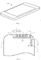
- FIG. 1 is a schematic diagram of an electronic device 100 according to an exemplary embodiment.
- FIG. 2 is a partial schematic diagram of an electronic device 100 according to an exemplary embodiment.
- the electronic device 100 may include a middle frame 1, the middle frame 1 may include a slit 11, a first strip groove 12 and a second strip groove 13, the slit 11 may be formed by extending inward from an edge of the middle frame 1 and may be communicated to the first strip groove 12 and the second strip groove 13, one end of the first strip groove 12 and one end of the second strip groove 13 are close to each other, and the first strip groove 12 and the second strip groove 13 may be disposed close to the edge of the middle frame 1, so that the portions from the edges of the strip grooves to the edge of the middle frame 1 may be used as portions of an antenna.
- the first strip groove 12 and the second strip groove 13 may also be perpendicular to each other.
- the first strip groove 12 may be disposed along a width direction of the middle frame 11
- the second strip groove 13 may be disposed along a length direction of the middle frame 11.
- the electronic device 100 may also include a first grounding point 2 and a second grounding point 3, the first grounding point 2 is positioned at one end of the first strip groove 12 away from the second strip groove 13, and similarly, the second grounding point 3 is positioned at one end of the second strip groove 13 away from the first strip groove 12.
- the electronic device 100 may also include a data signal feed point 4, a frequency modulation circuit 5 and an NFC feed point 6, the data signal feed point 4, the frequency modulation circuit 5 and the NFC feed point 6 are positioned on a same side of the slit 11 as the first grounding point 2, and are positioned on a different side of the slit 11 from the side where the second grounding point 3 is positioned. As shown in FIG. 2 , the data signal feed point 4, the frequency modulation circuit 5 and the NFC feed point 6 are positioned above an extension line of the slit 11, and the second grounding point 3 is positioned below the extension line of the slit 11.
- the data signal feed point 4, the frequency modulation circuit 5 and the first grounding point 2 may cooperatively radiate 2G communication signals, 3G communication signals or 4G communication signals; the data signal feed point 4, the NFC feed point 6, the middle frame 1, the slit 11 and the second grounding point 3 may cooperatively radiate 5G communication signals; and the NFC feed point 6 and the first grounding point 2 may cooperatively radiate NFC signals.
- a communication antenna for 2G communication, 3G communication and 4G communication, a communication antenna for 5G communication and an antenna for NFC in the present disclosure may be partially shared, and a data communication function and an NFC function of the electronic device 100 may be realized simultaneously, thus the space occupied by antennas is reduced, which is beneficial for the internal layout of the electronic device 100.
- a frequency modulation circuit 5 may include a first switch 51, a second switch 52 and a tuning circuit 53.
- the first switch 51, the second switch 52 and the data signal feed point 4 are sequentially disposed in a direction from the first grounding point 2 to the slit 11, the first switch 51 is connected in series with the second switch 52, and the second switch 52 is electrically connected with the data signal feed point 4, so that full-band coverage of 2G communication, 3G communication and 4G communication is realized by adjusting the first switch 51, the second switch 52 and the tuning circuit 53.
- the first switch 51 may adopt a QM13144 type switch as shown in FIG. 3
- the second switch 52 may adopt a QM13136 type switch as shown in FIG. 4
- the first switch 51 may include switches RF1, RF2, RF3 and RF4, and similarly, the second switch 52 may also include switches RF1, RF2, RF3 and RF4.
- the state adjustment of the first switch 51 and the second switch 52 may be as shown in FIG. 5 .
- the switch RF3 of the first switch 51 may be turned on, and the switches RF1, RF2, RF3 and RF4 of the second switch 52 may be turned off.
- the switch RF4 of the first switch 51 when signals of N41 are radiated, the switch RF4 of the first switch 51 may be turned on, and the switch RF4 of the second switch 52 may be turned off. Still as shown in FIG. 5 , during signal radiation of other bands, the first switch 51 and the second switch 52 may have corresponding different states.
- the antenna signals of other bands may also be radiated, and the present disclosure will not be exemplified one by one.
- the NFC feed point 6 and the data signal feed point 4 may be adjacently disposed, the data signal feed point 4 and the slit 11 are positioned at two sides of the NFC feed point 6, and the NFC feed point 6 is electrically connected to the data communication feed point 3. Therefore, as shown in FIG. 6 , when the electronic device 100 is in a 5G communication state, an antenna signal received by the data signal feed point 4 may be output to the NFC feed point 6, further output to the middle frame 7 through a grounding end of the NFC feed point 6 and then coupled to another edge of the slit 11 via the slit 11, and finally flows into the second grounding point 3.
- the electronic device 100 may also include a 5G tuning circuit 7, the 5G tuning circuit 7 is connected in parallel with a signal receiving end 61 of the NFC feed point 6, the 5G tuning circuit 7 may be configured to adjust the communication band of 5G communication signals, and the signal receiving end 61 may be configured to receive NFC signals.
- the band during 5G communication may be adjusted by the tuning circuit, and a stopband can be formed for the NFC band, thereby ensuring that the NFC signals can be output from the NFC feed point 6 to the first grounding point 2.
- the 5G tuning circuit 7 may include a first capacitor 71 and a second capacitor 72 connected in series.
- the band of the 5G communication signals may be adjusted; and on the other hand, since the manufacturing accuracy of a single capacitor tends to be lower than the theoretical requirement, the present disclosure adopts the two capacitors connected in series to reduce the requirement for the manufacturing accuracy and reduce the amplitude of antenna offset.
- a capacitance of the first capacitor 71 may be 0.7 pF
- a capacitance of the second capacitor 72 may be 0.9 pF.
- the electronic device 100 may also include a high-frequency suppression circuit 8, the high-frequency suppression circuit 8 is connected in series with another signal receiving end 62 of the NFC feed point 6, and the high-frequency suppression circuit 8 is configured to suppress the 5G communication signals.
- the high-frequency suppression circuit 8 may include an inductor 81 having an inductance greater than a preset threshold.
- the inductance of the inductor 81 may be 68 nH, 60 nH, 70 nH, or the like. The present disclosure is not limited thereto.
- the electronic device 100 may also include a circuit board (not shown), the circuit board is electrically connected with the first switch 51, the second switch 52, the NFC feed point 6 and the data signal feed point 4, and the inductor 81 may also be welded on the circuit board.
- the circuit board since the inductance of the inductor 81 is larger, the welding point between the inductor 81 and the circuit board is too large, and the loading capacitance is easily formed, resulting in frequency offset. Therefore, in the present disclosure, the circuit board includes a hollowed-out area corresponding to the inductor 81 so as to reduce the frequency offset and reduce the parasitic capacitance.
Landscapes
- Engineering & Computer Science (AREA)
- Computer Networks & Wireless Communication (AREA)
- Signal Processing (AREA)
- Near-Field Transmission Systems (AREA)
- Support Of Aerials (AREA)
Abstract
Description
- The present disclosure relates to the technical field of electronic terminals, and particularly relates to an electronic device.
- With the development of the mobile communication technology, it has become an urgent need at present to configure second generation (2G), third generation (3G), fourth generation (4G) and fifth generation (5G) communication functions for an electronic device. Furthermore, in order to facilitate the user's travel, the electronic device may generally have a near field communication (NFC) function. In order to be compatible with the above communication functions, how to configure an antenna in the electronic device has become an important topic.
- Accordingly, the present disclosure provides an electronic device to solve the defects in related technologies.
- An embodiment of the present disclosure provides an electronic device, including: a middle frame, wherein the middle frame includes a slit, a first strip groove and a second strip groove, the slit extends inward from an edge of the middle frame so as to be communicated to the first strip groove and the second strip groove, and one end of the first strip groove and one end of the second strip groove are close to each other; a first grounding point, wherein the first grounding point is positioned at one end of the first strip groove away from the second strip groove; a second grounding point, wherein the second grounding point is positioned at one end of the second strip groove away from the first strip groove, and the first grounding point and the second grounding point are respectively positioned at two sides of the slit; and a data signal feed point, a frequency modulation circuit and a near field communication (NFC) feed point, wherein the data signal feed point, the frequency modulation circuit and the NFC feed point as well as the first grounding point are positioned on a same side of the slit; the data signal feed point, the frequency modulation circuit and the first grounding point cooperatively radiate 2G communication signals, 3G communication signals or 4G communication signals, the data signal feed point, the NFC feed point, the middle frame, the slit and the second grounding point cooperatively radiate 5G communication signals, and the NFC feed point and the first grounding point cooperatively radiate NFC signals.
- The technical solutions provided by the embodiments of the present disclosure may have beneficial effects as follows. As can be seen from the above embodiments, a communication antenna for 2G communication, 3G communication and 4G communication, a communication antenna for 5G communication and an antenna for NFC in the present disclosure may be partially shared, and a data communication function and an NFC function of an electronic device may be realized simultaneously, thus the space occupied by antennas is reduced, which is beneficial for the internal layout of the electronic device.
- According to an exemplary embodiment, the frequency modulation circuit includes a first switch, a second switch and a tuning circuit, and full-band coverage of 2G communication, 3G communication or 4G communication is implemented by adjusting the first switch, the second switch and the tuning circuit.
- According to an exemplary embodiment, the electronic device also includes a tuning circuit, wherein the tuning circuit is connected in parallel with a signal receiving end of the NFC feed point, and the tuning circuit is configured to adjust a communication band of the 5G communication signals.
- According to an exemplary embodiment, the tuning circuit includes a first capacitor and a second capacitor connected in series.
- According to an exemplary embodiment, a capacitance of the first capacitor is 0.7 pF, and a capacitance of the second capacitor is 0.9 pF.
- According to an exemplary embodiment, the electronic device also includes a high-frequency suppression circuit, wherein the high-frequency suppression circuit is connected in series with a signal receiving end of the NFC feed point, and the high-frequency suppression circuit is configured to suppress the 5G communication signals.
- According to an exemplary embodiment, the high-frequency suppression circuit includes an inductor having an inductance greater than a preset threshold.
- According to an exemplary embodiment, the inductance of the inductor is 68 nH.
- According to an exemplary embodiment, the electronic device also includes a circuit board, wherein the frequency modulation circuit, the NFC feed point and the data signal feed point are connected to the circuit board, and the circuit board includes a hollowed-out area corresponding to the inductor.
- According to an exemplary embodiment, the first strip groove and the second strip groove are perpendicular to each other.
- It should be understood that the above general description and the following detailed description are merely exemplary and explanatory, but they are not intended to limit the present disclosure.
- The accompanying drawings, which are incorporated in and constitute a part of this specification, illustrate embodiments consistent with the present disclosure and, together with the description, serve to explain the principles of the present disclosure.
-
FIG. 1 is a schematic diagram of an electronic device according to an exemplary embodiment. -
FIG. 2 is a partial schematic diagram of an electronic device according to an exemplary embodiment. -
FIG. 3 is a circuit schematic diagram of a first switch according to an exemplary embodiment. -
FIG. 4 is a circuit schematic diagram of a second switch according to an exemplary embodiment. -
FIG. 5 is a schematic diagram of frequency modulation according to an exemplary embodiment. -
FIG. 6 is a partial schematic diagram of another electronic device according to an exemplary embodiment. -
FIG. 7 is a schematic diagram of connection between an NFC feed point and a tuning circuit according to an exemplary embodiment. -
FIG. 8 is a schematic diagram of connection between an NFC feed point and a high-frequency suppression circuit according to an exemplary embodiment. - Reference will now be made in detail to exemplary embodiments, examples of which are illustrated in the accompanying drawings. The following description refers to the accompanying drawings in which the same numbers in different drawings represent the same or similar elements unless otherwise represented. The implementations set forth in the following description of exemplary embodiments do not represent all implementations consistent with the present disclosure. Instead, they are merely examples of apparatuses and methods consistent with aspects related to the present disclosure as recited in the appended claims.
- The terms used in the present disclosure are for the purpose of describing specific embodiments only, and are not intended to limit the present disclosure. The singular forms "a", "the" and "this" used in the present disclosure and the appended claims may also include plural forms unless the contexts clearly indicate other meanings. It should also be understood that the term "and/or" used herein refers to and includes any and all possible combinations of one or more of the associated listed items.
- It should be understood that although the terms "first", "second" and "third" may be adopted in the present disclosure to describe various information, these information should not be limited to these terms. These terms are only used to distinguish the same type of information from each other. For example, the first information may also be referred to as the second information without departing from the scope of the present disclosure. Similarly, the second information may also be referred to as the first information. Depending on the context, the word "if" as used herein may be interpreted as "when" or "while" or "in response to determining".
-
FIG. 1 is a schematic diagram of anelectronic device 100 according to an exemplary embodiment.FIG. 2 is a partial schematic diagram of anelectronic device 100 according to an exemplary embodiment. As shown inFIG. 1 and FIG. 2 , theelectronic device 100 may include a middle frame 1, the middle frame 1 may include aslit 11, afirst strip groove 12 and asecond strip groove 13, theslit 11 may be formed by extending inward from an edge of the middle frame 1 and may be communicated to thefirst strip groove 12 and thesecond strip groove 13, one end of thefirst strip groove 12 and one end of thesecond strip groove 13 are close to each other, and thefirst strip groove 12 and thesecond strip groove 13 may be disposed close to the edge of the middle frame 1, so that the portions from the edges of the strip grooves to the edge of the middle frame 1 may be used as portions of an antenna. Thefirst strip groove 12 and thesecond strip groove 13 may also be perpendicular to each other. For example, as shown inFIG. 2 , thefirst strip groove 12 may be disposed along a width direction of themiddle frame 11, and thesecond strip groove 13 may be disposed along a length direction of themiddle frame 11. - Further, the
electronic device 100 may also include afirst grounding point 2 and asecond grounding point 3, thefirst grounding point 2 is positioned at one end of thefirst strip groove 12 away from thesecond strip groove 13, and similarly, thesecond grounding point 3 is positioned at one end of the second strip groove 13 away from thefirst strip groove 12. Theelectronic device 100 may also include a datasignal feed point 4, afrequency modulation circuit 5 and anNFC feed point 6, the datasignal feed point 4, thefrequency modulation circuit 5 and theNFC feed point 6 are positioned on a same side of theslit 11 as thefirst grounding point 2, and are positioned on a different side of theslit 11 from the side where thesecond grounding point 3 is positioned. As shown inFIG. 2 , the datasignal feed point 4, thefrequency modulation circuit 5 and theNFC feed point 6 are positioned above an extension line of theslit 11, and thesecond grounding point 3 is positioned below the extension line of theslit 11. - The data
signal feed point 4, thefrequency modulation circuit 5 and thefirst grounding point 2 may cooperatively radiate 2G communication signals, 3G communication signals or 4G communication signals; the datasignal feed point 4, theNFC feed point 6, the middle frame 1, theslit 11 and thesecond grounding point 3 may cooperatively radiate 5G communication signals; and theNFC feed point 6 and thefirst grounding point 2 may cooperatively radiate NFC signals. - As can be seen from the above embodiments, a communication antenna for 2G communication, 3G communication and 4G communication, a communication antenna for 5G communication and an antenna for NFC in the present disclosure may be partially shared, and a data communication function and an NFC function of the
electronic device 100 may be realized simultaneously, thus the space occupied by antennas is reduced, which is beneficial for the internal layout of theelectronic device 100. - In an embodiment, as shown in
FIG. 2 , afrequency modulation circuit 5 may include afirst switch 51, asecond switch 52 and a tuning circuit 53. Thefirst switch 51, thesecond switch 52 and the datasignal feed point 4 are sequentially disposed in a direction from thefirst grounding point 2 to theslit 11, thefirst switch 51 is connected in series with thesecond switch 52, and thesecond switch 52 is electrically connected with the datasignal feed point 4, so that full-band coverage of 2G communication, 3G communication and 4G communication is realized by adjusting thefirst switch 51, thesecond switch 52 and the tuning circuit 53. - For example, the
first switch 51 may adopt a QM13144 type switch as shown inFIG. 3 , and thesecond switch 52 may adopt a QM13136 type switch as shown inFIG. 4 . Thefirst switch 51 may include switches RF1, RF2, RF3 and RF4, and similarly, thesecond switch 52 may also include switches RF1, RF2, RF3 and RF4. The state adjustment of thefirst switch 51 and thesecond switch 52 may be as shown inFIG. 5 . When signals of GSM850 are radiated, the switch RF3 of thefirst switch 51 may be turned on, and the switches RF1, RF2, RF3 and RF4 of thesecond switch 52 may be turned off. For another example, when signals of N41 are radiated, the switch RF4 of thefirst switch 51 may be turned on, and the switch RF4 of thesecond switch 52 may be turned off. Still as shown inFIG. 5 , during signal radiation of other bands, thefirst switch 51 and thesecond switch 52 may have corresponding different states. Of course, in addition to the antenna signals of the bands as shown inFIG. 5 , the antenna signals of other bands may also be radiated, and the present disclosure will not be exemplified one by one. - In another embodiment, as shown in
FIG. 6 , theNFC feed point 6 and the datasignal feed point 4 may be adjacently disposed, the datasignal feed point 4 and theslit 11 are positioned at two sides of theNFC feed point 6, and theNFC feed point 6 is electrically connected to the datacommunication feed point 3. Therefore, as shown inFIG. 6 , when theelectronic device 100 is in a 5G communication state, an antenna signal received by the datasignal feed point 4 may be output to theNFC feed point 6, further output to themiddle frame 7 through a grounding end of theNFC feed point 6 and then coupled to another edge of theslit 11 via theslit 11, and finally flows into thesecond grounding point 3. - In each of the above embodiments, as shown in
FIG. 7 , theelectronic device 100 may also include a5G tuning circuit 7, the5G tuning circuit 7 is connected in parallel with asignal receiving end 61 of theNFC feed point 6, the5G tuning circuit 7 may be configured to adjust the communication band of 5G communication signals, and thesignal receiving end 61 may be configured to receive NFC signals. Based on the above, the band during 5G communication may be adjusted by the tuning circuit, and a stopband can be formed for the NFC band, thereby ensuring that the NFC signals can be output from theNFC feed point 6 to thefirst grounding point 2. - For example, as shown in
FIG. 7 , the5G tuning circuit 7 may include afirst capacitor 71 and asecond capacitor 72 connected in series. Through the two capacitors connected in series, on the one hand, the band of the 5G communication signals may be adjusted; and on the other hand, since the manufacturing accuracy of a single capacitor tends to be lower than the theoretical requirement, the present disclosure adopts the two capacitors connected in series to reduce the requirement for the manufacturing accuracy and reduce the amplitude of antenna offset. For example, a capacitance of thefirst capacitor 71 may be 0.7 pF, and a capacitance of thesecond capacitor 72 may be 0.9 pF. - Similarly, as shown in
FIG. 8 , theelectronic device 100 may also include a high-frequency suppression circuit 8, the high-frequency suppression circuit 8 is connected in series with anothersignal receiving end 62 of theNFC feed point 6, and the high-frequency suppression circuit 8 is configured to suppress the 5G communication signals. For example, the high-frequency suppression circuit 8 may include aninductor 81 having an inductance greater than a preset threshold. For example, the inductance of theinductor 81 may be 68 nH, 60 nH, 70 nH, or the like. The present disclosure is not limited thereto. - In the present embodiment, the
electronic device 100 may also include a circuit board (not shown), the circuit board is electrically connected with thefirst switch 51, thesecond switch 52, theNFC feed point 6 and the data signalfeed point 4, and theinductor 81 may also be welded on the circuit board. In fact, since the inductance of theinductor 81 is larger, the welding point between theinductor 81 and the circuit board is too large, and the loading capacitance is easily formed, resulting in frequency offset. Therefore, in the present disclosure, the circuit board includes a hollowed-out area corresponding to theinductor 81 so as to reduce the frequency offset and reduce the parasitic capacitance. - Other embodiments of the present disclosure will be apparent to those skilled in the art from consideration of the specification and practice of the disclosure here. The present disclosure is intended to cover any variations, uses, or adaptations of the present disclosure following the general principles thereof and including such departures from the present disclosure as come within known or customary practice in the art. It is intended that the specification and embodiments be considered as exemplary only, with a true scope and spirit of the present disclosure being indicated by the following claims.
- It will be appreciated that the present disclosure is not limited to the exact construction that has been described above and illustrated in the accompanying drawings, and that various modifications and changes can be made without departing from the scope thereof. It is intended that the scope of the present disclosure only be limited by the appended claims.
Claims (13)
- An electronic device, characterized in that, the electronic device comprises:a middle frame (1), wherein the middle frame (1) comprises a slit (11), a first strip groove (12) and a second strip groove (13), wherein the slit (11) extends inward from an edge of the middle frame (1) so as to be communicated to the first strip groove (12) and the second strip groove (13), and one end of the first strip groove (12) and one end of the second strip groove (13) are close to each other;a first grounding point (2), wherein the first grounding point (2) is positioned at one end of the first strip groove (12) away from the second strip groove (13);a second grounding point (3), wherein the second grounding point (3) is positioned at one end of the second strip groove (13) away from the first strip groove (12), and the first grounding point (2) and the second grounding point (3) are respectively positioned at two sides of the slit (11); anda data signal feed point (4), a frequency modulation circuit (5) and a near field communication, NFC, feed point (6), wherein the data signal feed point (4), the frequency modulation circuit (5) and the NFC feed point (6) as well as the first grounding point (2) are positioned on a same side of the slit (11);wherein the data signal feed point (4), the frequency modulation circuit (5) and the first grounding point (2) cooperatively radiate second generation, 2G, communication signals, third generation, 3G, communication signals or fourth generation, 4G, communication signals, the data signal feed point (4), the NFC feed point (6), the middle frame (1), the slit (11) and the second grounding point (3) cooperatively radiate fifth generation, 5G, communication signals, and the NFC feed point (6) and the first grounding point (2) cooperatively radiate NFC signals.
- The electronic device of claim 1, wherein the frequency modulation circuit (5) comprises a first switch (51), a second switch (52) and a tuning circuit (53), and full-band coverage of 2G communication, 3G communication or 4G communication is implemented by adjusting the first switch (51), the second switch (52) and the tuning circuit (53).
- The electronic device of claim 1, wherein the NFC feed point (6) is adjacent to the data signal feed point (4), and the data signal feed point (4) and the slit (11) are positioned at two sides of the NFC feed point (6), wherein the NFC feed point (6) is electrically connected to the data signal feed point (4) to form a path for 5G communication signals.
- The electronic device of claim 1, further comprising a 5G tuning circuit (7), wherein the 5G tuning circuit (7) is connected in parallel with a signal receiving end (61) of the NFC feed point (6), and the 5G tuning circuit (7) is configured to adjust a communication band of the 5G communication signals.
- The electronic device of claim 4, wherein the 5G tuning circuit (7) comprises a first capacitor (71) and a second capacitor (72) connected in series.
- The electronic device of claim 5, wherein a capacitance of the first capacitor (71) is 0.7 pF, and a capacitance of the second capacitor (72) is 0.9 pF.
- The electronic device of claim 1, further comprising a high-frequency suppression circuit (8), wherein the high-frequency suppression circuit (8) is connected in series with a signal receiving end (62) of the NFC feed point (6), and the high-frequency suppression circuit (8) is configured to suppress the 5G communication signals.
- The electronic device of claim 7, wherein the high-frequency suppression circuit (8) comprises an inductor having an inductance greater than a preset threshold.
- The electronic device of claim 8, wherein the inductance of the inductor is 68 nH.
- The electronic device of claim 8, further comprising a circuit board, wherein the frequency modulation circuit (5), the NFC feed point (6) and the data signal feed point (4) are connected to the circuit board, and the circuit board comprises a hollowed-out area corresponding to the inductor.
- The electronic device of claim 1, wherein the first strip groove (12) and the second strip groove (13) are perpendicular to each other.
- The electronic device of claim 1, wherein the first strip groove (12) is disposed along a width direction of the middle frame (1), and the second strip groove (13) is disposed along a length direction of the middle frame (1).
- The electronic device of claim 1, wherein the first strip groove (12) and the second strip groove (13) are disposed close to the edge of the middle frame (1), so that portions from edges of the strip grooves to the edge of the middle frame (1) are used as portions of an antenna.
Applications Claiming Priority (1)
| Application Number | Priority Date | Filing Date | Title |
|---|---|---|---|
| CN201910888073.1A CN112531320B (en) | 2019-09-19 | 2019-09-19 | Electronic equipment |
Publications (2)
| Publication Number | Publication Date |
|---|---|
| EP3796565A1 true EP3796565A1 (en) | 2021-03-24 |
| EP3796565B1 EP3796565B1 (en) | 2025-09-03 |
Family
ID=69174420
Family Applications (1)
| Application Number | Title | Priority Date | Filing Date |
|---|---|---|---|
| EP20152243.0A Active EP3796565B1 (en) | 2019-09-19 | 2020-01-16 | Electronic device |
Country Status (3)
| Country | Link |
|---|---|
| US (1) | US11088727B2 (en) |
| EP (1) | EP3796565B1 (en) |
| CN (1) | CN112531320B (en) |
Families Citing this family (1)
| Publication number | Priority date | Publication date | Assignee | Title |
|---|---|---|---|---|
| CN218415017U (en) * | 2022-08-09 | 2023-01-31 | 荣耀终端有限公司 | Antenna system and terminal equipment |
Citations (3)
| Publication number | Priority date | Publication date | Assignee | Title |
|---|---|---|---|---|
| CN105514624A (en) * | 2015-12-23 | 2016-04-20 | 广东欧珀移动通信有限公司 | Mobile terminal antenna system and mobile terminal |
| CN108736130A (en) * | 2018-07-11 | 2018-11-02 | Oppo广东移动通信有限公司 | Antenna module and electronic equipment |
| US10158384B1 (en) * | 2017-09-08 | 2018-12-18 | Apple Inc. | Electronic devices with indirectly-fed adjustable slot elements |
Family Cites Families (12)
| Publication number | Priority date | Publication date | Assignee | Title |
|---|---|---|---|---|
| EP1594188B1 (en) * | 2003-02-03 | 2010-04-14 | Panasonic Corporation | Antenna device and wireless communication device using same |
| CN105515599A (en) * | 2014-09-30 | 2016-04-20 | 深圳富泰宏精密工业有限公司 | Wireless communication device |
| CN204424427U (en) * | 2014-12-29 | 2015-06-24 | 上海安费诺永亿通讯电子有限公司 | A kind of adjustable antenna for all-metal construction communication terminal device |
| CN107275761A (en) * | 2016-04-08 | 2017-10-20 | 北京小米移动软件有限公司 | The antenna of terminal |
| CN107275753B (en) * | 2016-04-08 | 2020-06-19 | 北京小米移动软件有限公司 | terminal's antenna |
| TWI650904B (en) * | 2016-07-21 | 2019-02-11 | 群邁通訊股份有限公司 | Antenna structure and wireless communication device with same |
| CN107453056B (en) * | 2017-06-22 | 2020-08-21 | 瑞声科技(新加坡)有限公司 | Antenna system and communication equipment |
| TWI678028B (en) * | 2017-12-12 | 2019-11-21 | 群邁通訊股份有限公司 | Antenna structure and wireless communication device with same |
| CN108346849A (en) * | 2017-12-29 | 2018-07-31 | 瑞声精密制造科技(常州)有限公司 | A kind of antenna for mobile phone of metal edge frame |
| CN108832272B (en) * | 2018-05-29 | 2020-08-21 | 北京小米移动软件有限公司 | Electronic equipment and its antenna structure |
| CN208797179U (en) * | 2018-07-26 | 2019-04-26 | Oppo广东移动通信有限公司 | Antenna assembly and electronic device |
| CN109119758B (en) * | 2018-08-24 | 2021-03-12 | Oppo广东移动通信有限公司 | Antenna Components and Electronics |
-
2019
- 2019-09-19 CN CN201910888073.1A patent/CN112531320B/en active Active
-
2020
- 2020-01-15 US US16/743,713 patent/US11088727B2/en active Active
- 2020-01-16 EP EP20152243.0A patent/EP3796565B1/en active Active
Patent Citations (3)
| Publication number | Priority date | Publication date | Assignee | Title |
|---|---|---|---|---|
| CN105514624A (en) * | 2015-12-23 | 2016-04-20 | 广东欧珀移动通信有限公司 | Mobile terminal antenna system and mobile terminal |
| US10158384B1 (en) * | 2017-09-08 | 2018-12-18 | Apple Inc. | Electronic devices with indirectly-fed adjustable slot elements |
| CN108736130A (en) * | 2018-07-11 | 2018-11-02 | Oppo广东移动通信有限公司 | Antenna module and electronic equipment |
Also Published As
| Publication number | Publication date |
|---|---|
| US20210091824A1 (en) | 2021-03-25 |
| CN112531320A (en) | 2021-03-19 |
| EP3796565B1 (en) | 2025-09-03 |
| US11088727B2 (en) | 2021-08-10 |
| CN112531320B (en) | 2023-06-20 |
Similar Documents
| Publication | Publication Date | Title |
|---|---|---|
| US12562504B2 (en) | Antenna system and electronic device | |
| US12388181B2 (en) | Antenna assembly and electronic device | |
| US11688930B2 (en) | Antenna apparatus and mobile terminal | |
| US12418100B2 (en) | Antenna assembly and electronic device | |
| US6653977B1 (en) | Wireless handset | |
| CN108767499A (en) | Metal edge frame antenna and terminal device | |
| EP2424119A1 (en) | Antenna module and impedance matching method thereof | |
| US9385427B2 (en) | Multi-band antenna and wireless communication device employing same | |
| WO2021017625A1 (en) | Antenna module and mobile terminal | |
| WO2020134330A1 (en) | Antenna system and mobile terminal applying the antenna system | |
| CN112736459B (en) | Dual antenna systems, RF architecture and electronics | |
| US10763900B2 (en) | Antenna module,mobile terminal and method for tuning the antenna module | |
| EP3185354A1 (en) | Antenna component and electronic device | |
| WO2023071817A1 (en) | Antenna assembly, antenna device, and electronic equipment | |
| US9331398B2 (en) | Dual-mode terminal antenna and signal processing method | |
| CN108232407B (en) | LTE antenna based on comprehensive screen metal frame | |
| US11088727B2 (en) | Electronic device | |
| US9257755B2 (en) | Apparatus for controlling electric field distribution by utilizing short trace structures | |
| CN110459860B (en) | Rear shell assembly and electronic equipment | |
| CN112993568A (en) | Electronic equipment | |
| CN215869802U (en) | Antenna module and electronic equipment | |
| CN112751195A (en) | Terminal antenna system and mobile terminal | |
| CN110445917A (en) | a terminal | |
| CN113922082A (en) | Antenna module applied to terminal equipment and terminal equipment | |
| CN215896708U (en) | Metal frame antenna module and mobile phone |
Legal Events
| Date | Code | Title | Description |
|---|---|---|---|
| PUAI | Public reference made under article 153(3) epc to a published international application that has entered the european phase |
Free format text: ORIGINAL CODE: 0009012 |
|
| STAA | Information on the status of an ep patent application or granted ep patent |
Free format text: STATUS: THE APPLICATION HAS BEEN PUBLISHED |
|
| AK | Designated contracting states |
Kind code of ref document: A1 Designated state(s): AL AT BE BG CH CY CZ DE DK EE ES FI FR GB GR HR HU IE IS IT LI LT LU LV MC MK MT NL NO PL PT RO RS SE SI SK SM TR |
|
| AX | Request for extension of the european patent |
Extension state: BA ME |
|
| STAA | Information on the status of an ep patent application or granted ep patent |
Free format text: STATUS: REQUEST FOR EXAMINATION WAS MADE |
|
| 17P | Request for examination filed |
Effective date: 20210422 |
|
| RBV | Designated contracting states (corrected) |
Designated state(s): AL AT BE BG CH CY CZ DE DK EE ES FI FR GB GR HR HU IE IS IT LI LT LU LV MC MK MT NL NO PL PT RO RS SE SI SK SM TR |
|
| STAA | Information on the status of an ep patent application or granted ep patent |
Free format text: STATUS: EXAMINATION IS IN PROGRESS |
|
| 17Q | First examination report despatched |
Effective date: 20221223 |
|
| REG | Reference to a national code |
Ref country code: DE Ref legal event code: R079 Free format text: PREVIOUS MAIN CLASS: H04B0005000000 Ipc: H01Q0001240000 Ref country code: DE Ref legal event code: R079 Ref document number: 602020057829 Country of ref document: DE Free format text: PREVIOUS MAIN CLASS: H04B0005000000 Ipc: H01Q0001240000 |
|
| GRAP | Despatch of communication of intention to grant a patent |
Free format text: ORIGINAL CODE: EPIDOSNIGR1 |
|
| STAA | Information on the status of an ep patent application or granted ep patent |
Free format text: STATUS: GRANT OF PATENT IS INTENDED |
|
| RIC1 | Information provided on ipc code assigned before grant |
Ipc: H01Q 5/328 20150101ALI20250319BHEP Ipc: H04B 5/77 20240101ALI20250319BHEP Ipc: H01Q 13/10 20060101ALI20250319BHEP Ipc: H01Q 5/50 20150101ALI20250319BHEP Ipc: H01Q 5/35 20150101ALI20250319BHEP Ipc: H01Q 1/24 20060101AFI20250319BHEP |
|
| INTG | Intention to grant announced |
Effective date: 20250327 |
|
| P01 | Opt-out of the competence of the unified patent court (upc) registered |
Free format text: CASE NUMBER: APP_21382/2025 Effective date: 20250506 |
|
| GRAS | Grant fee paid |
Free format text: ORIGINAL CODE: EPIDOSNIGR3 |
|
| GRAA | (expected) grant |
Free format text: ORIGINAL CODE: 0009210 |
|
| STAA | Information on the status of an ep patent application or granted ep patent |
Free format text: STATUS: THE PATENT HAS BEEN GRANTED |
|
| AK | Designated contracting states |
Kind code of ref document: B1 Designated state(s): AL AT BE BG CH CY CZ DE DK EE ES FI FR GB GR HR HU IE IS IT LI LT LU LV MC MK MT NL NO PL PT RO RS SE SI SK SM TR |
|
| REG | Reference to a national code |
Ref country code: CH Ref legal event code: EP |
|
| REG | Reference to a national code |
Ref country code: DE Ref legal event code: R096 Ref document number: 602020057829 Country of ref document: DE |
|
| REG | Reference to a national code |
Ref country code: IE Ref legal event code: FG4D |
|
| REG | Reference to a national code |
Ref country code: NL Ref legal event code: MP Effective date: 20250903 |
|
| PGFP | Annual fee paid to national office [announced via postgrant information from national office to epo] |
Ref country code: GB Payment date: 20251127 Year of fee payment: 7 |
|
| PG25 | Lapsed in a contracting state [announced via postgrant information from national office to epo] |
Ref country code: NO Free format text: LAPSE BECAUSE OF FAILURE TO SUBMIT A TRANSLATION OF THE DESCRIPTION OR TO PAY THE FEE WITHIN THE PRESCRIBED TIME-LIMIT Effective date: 20251203 |
|
| REG | Reference to a national code |
Ref country code: LT Ref legal event code: MG9D |
|
| PG25 | Lapsed in a contracting state [announced via postgrant information from national office to epo] |
Ref country code: FI Free format text: LAPSE BECAUSE OF FAILURE TO SUBMIT A TRANSLATION OF THE DESCRIPTION OR TO PAY THE FEE WITHIN THE PRESCRIBED TIME-LIMIT Effective date: 20250903 |
|
| PG25 | Lapsed in a contracting state [announced via postgrant information from national office to epo] |
Ref country code: HR Free format text: LAPSE BECAUSE OF FAILURE TO SUBMIT A TRANSLATION OF THE DESCRIPTION OR TO PAY THE FEE WITHIN THE PRESCRIBED TIME-LIMIT Effective date: 20250903 |
|
| PG25 | Lapsed in a contracting state [announced via postgrant information from national office to epo] |
Ref country code: GR Free format text: LAPSE BECAUSE OF FAILURE TO SUBMIT A TRANSLATION OF THE DESCRIPTION OR TO PAY THE FEE WITHIN THE PRESCRIBED TIME-LIMIT Effective date: 20251204 |
|
| PG25 | Lapsed in a contracting state [announced via postgrant information from national office to epo] |
Ref country code: SE Free format text: LAPSE BECAUSE OF FAILURE TO SUBMIT A TRANSLATION OF THE DESCRIPTION OR TO PAY THE FEE WITHIN THE PRESCRIBED TIME-LIMIT Effective date: 20250903 |
|
| PG25 | Lapsed in a contracting state [announced via postgrant information from national office to epo] |
Ref country code: LV Free format text: LAPSE BECAUSE OF FAILURE TO SUBMIT A TRANSLATION OF THE DESCRIPTION OR TO PAY THE FEE WITHIN THE PRESCRIBED TIME-LIMIT Effective date: 20250903 |
|
| PG25 | Lapsed in a contracting state [announced via postgrant information from national office to epo] |
Ref country code: BG Free format text: LAPSE BECAUSE OF FAILURE TO SUBMIT A TRANSLATION OF THE DESCRIPTION OR TO PAY THE FEE WITHIN THE PRESCRIBED TIME-LIMIT Effective date: 20250903 Ref country code: PL Free format text: LAPSE BECAUSE OF FAILURE TO SUBMIT A TRANSLATION OF THE DESCRIPTION OR TO PAY THE FEE WITHIN THE PRESCRIBED TIME-LIMIT Effective date: 20250903 |
|
| PG25 | Lapsed in a contracting state [announced via postgrant information from national office to epo] |
Ref country code: RS Free format text: LAPSE BECAUSE OF FAILURE TO SUBMIT A TRANSLATION OF THE DESCRIPTION OR TO PAY THE FEE WITHIN THE PRESCRIBED TIME-LIMIT Effective date: 20251203 |
|
| PG25 | Lapsed in a contracting state [announced via postgrant information from national office to epo] |
Ref country code: ES Free format text: LAPSE BECAUSE OF FAILURE TO SUBMIT A TRANSLATION OF THE DESCRIPTION OR TO PAY THE FEE WITHIN THE PRESCRIBED TIME-LIMIT Effective date: 20250903 |
|
| REG | Reference to a national code |
Ref country code: AT Ref legal event code: MK05 Ref document number: 1834292 Country of ref document: AT Kind code of ref document: T Effective date: 20250903 |
|
| PG25 | Lapsed in a contracting state [announced via postgrant information from national office to epo] |
Ref country code: NL Free format text: LAPSE BECAUSE OF FAILURE TO SUBMIT A TRANSLATION OF THE DESCRIPTION OR TO PAY THE FEE WITHIN THE PRESCRIBED TIME-LIMIT Effective date: 20250903 |
|
| PG25 | Lapsed in a contracting state [announced via postgrant information from national office to epo] |
Ref country code: SM Free format text: LAPSE BECAUSE OF FAILURE TO SUBMIT A TRANSLATION OF THE DESCRIPTION OR TO PAY THE FEE WITHIN THE PRESCRIBED TIME-LIMIT Effective date: 20250903 |
|
| PGFP | Annual fee paid to national office [announced via postgrant information from national office to epo] |
Ref country code: DE Payment date: 20251126 Year of fee payment: 7 |
|
| PG25 | Lapsed in a contracting state [announced via postgrant information from national office to epo] |
Ref country code: AT Free format text: LAPSE BECAUSE OF FAILURE TO SUBMIT A TRANSLATION OF THE DESCRIPTION OR TO PAY THE FEE WITHIN THE PRESCRIBED TIME-LIMIT Effective date: 20250903 |
|
| PG25 | Lapsed in a contracting state [announced via postgrant information from national office to epo] |
Ref country code: IT Free format text: LAPSE BECAUSE OF FAILURE TO SUBMIT A TRANSLATION OF THE DESCRIPTION OR TO PAY THE FEE WITHIN THE PRESCRIBED TIME-LIMIT Effective date: 20250903 |
|
| PG25 | Lapsed in a contracting state [announced via postgrant information from national office to epo] |
Ref country code: IS Free format text: LAPSE BECAUSE OF FAILURE TO SUBMIT A TRANSLATION OF THE DESCRIPTION OR TO PAY THE FEE WITHIN THE PRESCRIBED TIME-LIMIT Effective date: 20260103 |
|
| PG25 | Lapsed in a contracting state [announced via postgrant information from national office to epo] |
Ref country code: PT Free format text: LAPSE BECAUSE OF FAILURE TO SUBMIT A TRANSLATION OF THE DESCRIPTION OR TO PAY THE FEE WITHIN THE PRESCRIBED TIME-LIMIT Effective date: 20260105 Ref country code: CZ Free format text: LAPSE BECAUSE OF FAILURE TO SUBMIT A TRANSLATION OF THE DESCRIPTION OR TO PAY THE FEE WITHIN THE PRESCRIBED TIME-LIMIT Effective date: 20250903 |
|
| PG25 | Lapsed in a contracting state [announced via postgrant information from national office to epo] |
Ref country code: SK Free format text: LAPSE BECAUSE OF FAILURE TO SUBMIT A TRANSLATION OF THE DESCRIPTION OR TO PAY THE FEE WITHIN THE PRESCRIBED TIME-LIMIT Effective date: 20250903 Ref country code: EE Free format text: LAPSE BECAUSE OF FAILURE TO SUBMIT A TRANSLATION OF THE DESCRIPTION OR TO PAY THE FEE WITHIN THE PRESCRIBED TIME-LIMIT Effective date: 20250903 |