EP3796208A1 - Fingerprint recognition apparatus and electronic device - Google Patents
Fingerprint recognition apparatus and electronic device Download PDFInfo
- Publication number
- EP3796208A1 EP3796208A1 EP18942800.6A EP18942800A EP3796208A1 EP 3796208 A1 EP3796208 A1 EP 3796208A1 EP 18942800 A EP18942800 A EP 18942800A EP 3796208 A1 EP3796208 A1 EP 3796208A1
- Authority
- EP
- European Patent Office
- Prior art keywords
- light
- emitting pixel
- optical sensing
- array
- fingerprint identification
- Prior art date
- Legal status (The legal status is an assumption and is not a legal conclusion. Google has not performed a legal analysis and makes no representation as to the accuracy of the status listed.)
- Granted
Links
Images


Classifications
-
- G—PHYSICS
- G06—COMPUTING OR CALCULATING; COUNTING
- G06V—IMAGE OR VIDEO RECOGNITION OR UNDERSTANDING
- G06V40/00—Recognition of biometric, human-related or animal-related patterns in image or video data
- G06V40/10—Human or animal bodies, e.g. vehicle occupants or pedestrians; Body parts, e.g. hands
- G06V40/12—Fingerprints or palmprints
- G06V40/13—Sensors therefor
- G06V40/1318—Sensors therefor using electro-optical elements or layers, e.g. electroluminescent sensing
-
- G—PHYSICS
- G06—COMPUTING OR CALCULATING; COUNTING
- G06V—IMAGE OR VIDEO RECOGNITION OR UNDERSTANDING
- G06V40/00—Recognition of biometric, human-related or animal-related patterns in image or video data
- G06V40/10—Human or animal bodies, e.g. vehicle occupants or pedestrians; Body parts, e.g. hands
- G06V40/12—Fingerprints or palmprints
- G06V40/13—Sensors therefor
- G06V40/1329—Protecting the fingerprint sensor against damage caused by the finger
Definitions
- Embodiments of the present application relate to the field of communications, and more particularly, to a fingerprint identification apparatus and an electronic device.
- An under-screen optical fingerprint system is generally composed of a plurality of laminated layers. From top to bottom, a typical laminated layer structure includes a finger for image capturing, an organic light-emitting diode (Organic Light-Emitting Diode, OLED) screen, an optical imaging component, and an optical sensor.
- OLED Organic Light-Emitting Diode
- OLED Organic Light-Emitting Diode
- the structural form of the OLED screen is similar to the structural form of the optical sensor, the optical sensor will generate moire fringes when imaging based on light transmitted through the display screen, thereby affecting fingerprint identification performance.
- a fingerprint identification apparatus and an electronic device, which are capable of effectively increasing fingerprint identification performance.
- a fingerprint identification apparatus including:
- a range of the space period of the optical sensing array is 1um-20um.
- the space period of the optical sensing array is 5.
- the space period of the optical sensing array is equal to the sum of a size of an optical sensing unit in the optical sensing array and a distance between two adjacent optical sensing units.
- the optical sensing array is configured to reduce the size of the optical sensing unit in the optical sensing array, so that N ⁇ M/2K.
- the optical sensing array is configured to reduce the distance between the two adjacent optical sensing units in the optical sensing array, so that N ⁇ M/2K.
- the fingerprint identification apparatus further includes:
- a value range of the K is 1-20.
- the optical component is configured to reduce the K, so that N ⁇ M/2K.
- the optical component includes: a lens, wherein the K is a ratio between an object distance of the lens and an image distance of the lens.
- the lens is configured to reduce the object distance of the lens, so that N ⁇ M/2K.
- the lens is configured to increase the image distance of the lens, so that N ⁇ M/2K.
- a row of the optical sensing array has an angel with a row of the light-emitting pixel array.
- a line of the optical sensing array has an angel with a row of the light-emitting pixel array.
- a range of the angle is -15° to 15°.
- an electronic device including:
- the fingerprint identification apparatus as described in the first aspect and any one of possible implementation manners of the first aspect, and a light-emitting pixel array in the display screen; an optical sensing array in the fingerprint identification apparatus configured to receive a light signal emitted by the light-emitting pixel array and formed after being reflected from a human finger, the light signal being used for fingerprint identification.
- a range of a space period of the light-emitting pixel array is 40um-120um.
- the space period of the light-emitting pixel array includes a plurality of light-emitting pixel units, and part of the light-emitting pixel units in the plurality of light-emitting pixel units serve as an excitation light source for the fingerprint identification apparatus.
- the other part of the light-emitting pixel units in the plurality of light-emitting pixel units are configured to emit a striped light spot.
- the space period of the light-emitting pixel array is equal to the sum of a size of a light-emitting pixel unit in the light-emitting pixel array and a distance between two adjacent light-emitting pixel units.
- the light-emitting pixel array is configured to increase the size of the light-emitting pixel unit in the light-emitting pixel array, so that N ⁇ M/2K.
- the light-emitting pixel array is configured to increase the distance between the two adjacent light-emitting pixel units in the light-emitting pixel array, so that N ⁇ M/2K.
- the display screen is an organic light-emitting diode (OLED) display screen.
- OLED organic light-emitting diode
- the technical solutions in the embodiments of the present application can be applied to various electronic devices, for example, portable or mobile computing devices such as a smart phone, a notebook computer, a tablet computer and a game device, and other electronic devices such as an electronic database, an automobile and an automated teller machine (Automated Teller Machine, ATM), which is not limited in the embodiments of the present application.
- portable or mobile computing devices such as a smart phone, a notebook computer, a tablet computer and a game device
- other electronic devices such as an electronic database, an automobile and an automated teller machine (Automated Teller Machine, ATM), which is not limited in the embodiments of the present application.
- the technical solutions in the embodiments of the present application can be used for under-screen optical image capturing, for example, under-screen biometric identification or hidden under-screen camera function, and the biometric identification may include other biometric identification in addition to fingerprint identification, for example, living body identification and the like, which is not limited in the embodiments of the present application.
- under-screen biometric identification technology is first introduced below.
- the under-screen biometric identification technology refers to mounting a biometric identification module (such as a fingerprint identification module) under a display screen, thereby realizing a biometric identification operation inside a display area of the display screen, without setting a biometric capturing area in an area on the front of an electronic device other than the display area.
- a biometric identification module such as a fingerprint identification module
- the under-screen biometric identification technology uses light returned from a top surface of a display assembly of a device for fingerprint sensing and other sensing operations.
- the returned light carries information of an object (e.g., a finger) in contact with the top surface, and a particular optical sensor module located under a display screen is implemented by capturing and detecting the returned light.
- the optical sensor module may be designed to achieve desired optical imaging by properly configuring an optical element for capturing and detecting a returned light.
- FIG. 1 and FIG. 2 are schematic views showing an electronic device 100 to which under-screen biometric identification technology is applicable.
- FIG. 1 is schematic front view of the electronic device 100
- FIG. 2 is a partial schematic cross-sectional structural view of the electronic device 100 shown in FIG. 1 .
- the electronic device 100 may include a display screen 120 and a biometric identification module 140; and the display screen 120 has a display area 102, and the biometric identification module 140 is disposed under the display screen 120.
- the display screen 120 may be a self-emitting display screen that employs a self-emitting display unit as a display pixel.
- the display screen 120 may be an organic light-emitting diode (Organic Light-Emitting Diode, OLED) display screen or a micro light-emitting diode (Micro-LED) display screen.
- the display screen 120 may also be a liquid crystal display (Liquid Crystal Display, LCD) screen or other passive light-emitting display screens, which is not limited in the embodiments of the present application.
- the display screen 120 is specifically a touch display screen, which may not only display a screen but also detect a touch or press operation of a user, thereby providing the user with a human-machine interaction interface.
- the electronic device 100 may include a touch sensor, and the touch sensor may be specifically a touch panel (Touch Panel, TP), which may be disposed on a surface of the display screen 120, or may be partially integrated or entirely integrated into an interior of the display screen 120 to form a touch display screen.
- Touch Panel Touch Panel
- the biometric identification module 140 may be specifically an optical biometric identification module, such as an optical fingerprint module, which is mainly used for capturing biometric information (such as fingerprint image information) of a user.
- the biometric identification module 140 may be disposed at least in a partial area under the display screen 120 such that the biometric capturing area (or sensing area) 130 of the under-screen biometric identification module 140 is at least partially located in the display area 102 of the display screen 120.
- the biometric identification module 140 may include an optical image capturing apparatus, the optical image capturing apparatus may include a plurality of optical image capturing units, and the optical image capturing unit may specifically include a photo detector or a photoelectric sensor.
- the optical image capturing apparatus of the biometric identification module 140 may include a photo detector (Photo detector) array (or referred to as a photoelectric detector array, a photoelectric sensor array), including a plurality of photo detectors/photoelectric sensors distributed in an array.
- a photo detector Photo detector
- photoelectric detector array or referred to as a photoelectric detector array, a photoelectric sensor array
- the optical image capturing apparatus of the biometric identification module 140 may include an optical biometric sensor with an optical sensing array, such as an optical fingerprint sensor; and the optical sensing array includes a plurality of optical sensing units; the optical sensing unit may specifically include a photo detector or a photoelectric sensor, and an area where the optical sensing array is located or an optical sensing range corresponds to the biometric capturing area 130 of the biometric identification module 140.
- the biometric capturing area 130 is located in the display area 102 of the display screen 120. Therefore, when a user needs to unlock the electronic device 100 or perform other biometric verification, a biometric input operation can be implemented merely by pressing a finger on the biometric capturing area 130 located on the display screen 120. Since biometric capturing and detection can be implemented inside the display area 102 of the display screen 120, a front surface of the electronic device 100 in the above structure does not need to reserve space to set a fingerprint button (such as a Home button), and a full screen solution can be adopted. Therefore, the display area 102 of the display screen 120 can be substantially extended to the entire front surface of the electronic device 100.
- the display screen 120 adopting an OLED display screen is taken as an example, a light emitting layer of the display screen 120 has an array of OLED display units distributed in an array, and the biometric identification module 140 can utilize an OLED display unit (i.e., an OLED light source) of the OLED display screen 120 located in the biometric capturing area 130 as an excitation light source for biometric detection and identification.
- the biometric identification module 140 may also provide a light signal for biometric detection and identification by adopting an internal light source or an external light source.
- the optical image capturing unit can be applied not only to a self-emitting display screen such as an OLED display screen, but also to a non-self-emitting display screen such as a liquid crystal display screen or other passive light-emitting display screens.
- the biometric capturing area 130 When a finger touches, presses, or approaches (collectively referred to as pressing for convenience of description) the biometric capturing area 130, light emitted by the display unit of the biometric capturing area 130 is reflected by the finger to form reflected light.
- the reflected light may carry biometric information of a user's finger. For example, after the light is reflected by a fingerprint on the surface of the user's finger, since the reflected light of a fingerprint ridge is different from that of a fingerprint valley, the reflected light carries fingerprint information of the user.
- the reflected light is returned to the display screen 120, received by a photo detector array of the biometric identification module 140 underneath, and converted into a corresponding electrical signal, i.e., a biometric detection signal.
- the electronic device 100 can obtain biometric information of the user based on the biometric detection signal, and can further perform biometric matching verification, thereby completing identity verification of the current user so as to confirm whether the user has permission to perform a corresponding operation on
- the biometric identification module 140 may also be disposed in an entire area under the display screen 120 so as to extend the biometric capturing area 130 to the entire display area 102 of the display screen 120, thereby implementing full screen biometric identification.
- the electronic device 100 further includes a protective cover 110
- the cover 110 may be specifically a transparent cover such as a glass cover or a sapphire cover which is located on the display screen 120 and covers a front surface of the electronic device 100, and the surface of the protective cover 110 may also be provided with a protective layer. Therefore, in an embodiment of the present application, the so-called pressing finger against the display screen 120 actually refers to pressing the finger against the cover 110 on the display screen 120 or a surface of the protective layer covering the cover 110.
- a circuit board 150 such as a flexible printed circuit (Flexible Printed Circuit, FPC) may further be disposed under the biometric identification module 140.
- the biometric identification module 140 may be soldered to the circuit board 150 through a pad, and achieve electrical interconnection and signal transmission with other peripheral circuits or other elements of the electronic device 100 through the circuit board 150.
- the biometric identification module 140 may receive a control signal of a processing unit of the electronic device 100 through the circuit board 150, and may also output the biometric detection signal to the processing unit, a control unit or the like of the electronic device 100 through the circuit board 150.
- FIG. 3 is a schematic block diagram of a fingerprint identification system.
- the electronic device 100 may be composed of a plurality of laminated layers.
- the electronic device may include a finger for image capturing, an organic light-emitting diode (Organic Light-Emitting Diode, OLED) display screen, an optical imaging component, and a fingerprint sensor (sensor).
- the display screen may include a light-emitting pixel array; the light-emitting pixel array includes a plurality of light-emitting pixel units, and the light-emitting pixel units may specifically include a light-emitting diode, such as an organic light-emitting diode (Organic Light-Emitting Diode, OLED).
- the fingerprint sensor includes the optical sensing array, the optical sensing array includes a plurality of optical sensing units, and the optical sensing units may specifically include a photo detector or a photoelectric sensor.
- the optical sensor will generate moire fringes when imaging based on light transmitting through the display screen, thereby affecting fingerprint identification performance.
- the image captured by the fingerprint sensor may include a fingerprint image and a sampling pattern of the light-emitting pixel unit, and the sampling pattern of the light-emitting pixel unit may interfere with the fingerprint image at a constant angle and frequency, making the human eye unable to distinguish the fingerprint image and the sampling pattern of the light-emitting pixel unit.
- FIG. 4 is an example of an image with moire fringes captured by the fingerprint sensor.
- An embodiment of the present application provides a fingerprint identification apparatus, which can effectively solve the interference problem of moire fringes in the imaging system, thereby improving fingerprint identification performance.
- the fingerprint identification apparatus may include: a fingerprint sensor; and the fingerprint sensor including an optical sensing array, and a spatial period N of the optical sensing array satisfies N ⁇ M/2K, wherein M is a spatial period of a light-emitting pixel array, and K is a zoom ratio between an image displayed in a sensing area of the fingerprint sensor and an image captured in the sensing area by the fingerprint sensor.
- M/K is a period of the sampling pattern of the light-emitting pixel unit in the image captured by the fingerprint sensor.
- the period of the sampling pattern of the light-emitting pixel unit is twice greater than that of the fingerprint image.
- f1 is a capturing frequency of the sampling pattern of the light-emitting pixel unit
- f2 is a capturing frequency of the fingerprint image
- the capturing frequency of the fingerprint image is also twice greater than that of the sampling pattern of the light-emitting pixel unit.
- the fingerprint sensor samples the fingerprint image signal from a signal emitted by the light-emitting pixel unit; according to the sampling principle, the sampling frequency of the fingerprint image is twice greater than that of the sampling pattern of the light-emitting pixel unit, and thus avoiding under-sampling of the fingerprint image in the image captured by the fingerprint sensor, thereby avoiding moire fringes in the image captured by the fingerprint sensor, and improving fingerprint identification performance.
- the fingerprint identification apparatus further includes: an optical component, the optical component disposed above the optical sensing array, and configured to guide a light signal emitted by the light-emitting pixel array and reflected from a human finger to the optical sensing array.
- an optical sensing array in a fingerprint sensor can be configured to adjust a spatial period of the optical sensing array, so that N ⁇ M/2K.
- FIG. 5 is a schematic block diagram of an optical sensing array of a fingerprint sensor according to an embodiment of the present application.
- a space period N of the optical sensing array is equal to the sum of a size a of an optical sensing unit in the optical sensing array and a distance s between two adjacent optical sensing units.
- the optical sensing array may be configured to reduce the size of the optical sensing unit in the optical sensing array, so that N ⁇ M/2K. In other embodiments of the present application, the optical sensing array may be configured to reduce the distance between the two adjacent optical sensing units in the optical sensing array, so that N ⁇ M/2K.
- a second optical sensing array shown in FIG. 5 may reduce the distance s between the two adjacent optical sensing units, so that N ⁇ M/2K. For example, the distance s between the two adjacent optical sensing units is reduced, so that a+s ⁇ 4.925.
- a third optical sensing array shown in FIG. 5 may reduce the size a of the optical sensing unit in the optical sensing array, so that N ⁇ M/2K. For example, the size a of the optical sensing unit in the optical sensing array is reduced, so that a+s ⁇ 4.925.
- a fourth optical sensing array shown in FIG. 5 can simultaneously reduce the distance s between the two adjacent optical sensing units and the size a of the optical sensing unit in the optical sensing array, so that N ⁇ M/2K.
- the distance s between the two adjacent optical sensing units and the size a of the optical sensing unit in the optical sensing array are simultaneously reduced, so that a+s ⁇ 4.925.
- FIG. 5 is only an example of the embodiment of the present application and should not be understood as limitation on the present application.
- the optical sensing unit shown in FIG. 5 may further be designed into other shapes.
- the optical sensing unit may be a rectangular, circular, or elliptical optical sensing unit.
- the optical sensing array shown in FIG. 5 may further include a plurality of and/or a plurality of lines of optical sensing units.
- the optical sensing array shown in FIG. 5 can further be designed into other array shapes. For example, a circular array.
- the spatial period of the optical sensing array may refer to a distance between centers of the two adjacent optical sensing units in the optical sensing array.
- the space period of the optical sensing array may be greater than or smaller than the sum of the size of the optical sensing unit and the distance between the two adjacent optical sensing units.
- the optical sensing array may still be configured to reduce the size of the optical sensing unit in the optical sensing array and/or to reduce the distance between the two adjacent optical sensing units in the optical sensing array, so that N ⁇ M/2K. This is not limited in the embodiment of the present application.
- the K may be reduced, so that N ⁇ M/2K.
- the optical component may be configured to reduce the K, so that N ⁇ M/2K.
- the optical component is disposed above the optical sensing array, and configured to guide a light signal emitted by the light-emitting pixel array and reflected from a human finger to the optical sensing array.
- the optical component includes: a lens, wherein the K is a zoom ratio of the lens.
- FIG. 6 is a schematic view of an imaging principle of the optical component, when the optical component in the fingerprint identification apparatus according to an embodiment of the present application is a lens.
- the lens is configured to guide the light signal carrying information of an object (for example, a human finger) to the fingerprint sensor, so that the fingerprint sensor performs optical imaging based on the light signal.
- the K is the zoom ratio between the object and the image.
- the K is a ratio between an object distance of the lens and an image distance of the lens.
- P/Q ⁇ M/2N can be satisfied to further ensure N ⁇ M/2K.
- the P is the object distance of the lens
- the Q is the image distance of the lens
- the lens is configured to reduce the object distance P of the lens, so that N ⁇ M/2K.
- the lens is configured to increase the image distance Q of the lens, so that N ⁇ M/2K.
- the lens shown in FIG. 6 increases the image distance Q of the lens, so that N ⁇ M/2K.
- the image distance Q of the lens is increased, so that P/Q ⁇ 6.5.
- the lens shown in FIG. 6 reduces the object distance P of the lens, so that N ⁇ M/2K.
- the image distance Q of the lens is increased, so that P/Q ⁇ 6.5.
- the lens shown in FIG. 6 may simultaneously increase the image distance Q of the lens, so that N ⁇ M/2K.
- the lens may simultaneously increase the image distance Q of the lens, so that P/Q ⁇ 6.5.
- the optical component shown in FIG. 6 is only an example of the embodiment of the present application and should not be understood as limitation on the present application.
- a spatial period of a light-emitting pixel array in a display screen can be set or adjusted, so that N ⁇ M/2K.
- the light-emitting pixel unit in the light-emitting pixel array serve as an excitation light source of an optical sensing unit of an optical sensing array in a fingerprint sensor.
- FIG. 7 is a schematic block diagram of a light-emitting pixel array in a display screen according to an embodiment of the present application.
- a space period M of the light-emitting pixel array is equal to the sum of a size b of a light-emitting pixel unit in the light-emitting pixel array and a distance t between two adjacent light-emitting pixel units.
- the light-emitting pixel array may be configured to increase the size of the light-emitting pixel unit in the light-emitting pixel array, so that N ⁇ M/2K. In other embodiments of the present application, the light-emitting pixel array is configured to increase the distance between the two adjacent light-emitting pixel units in the light-emitting pixel array, so that N ⁇ M/2K.
- a second light-emitting pixel array shown in FIG. 7 may increase the distance t between the two adjacent light-emitting pixel units, so that N ⁇ M/2K. For example, the distance t between the two adjacent light-emitting pixel units is increased, so that b+t ⁇ 66.
- a third light-emitting pixel array shown in FIG. 7 may increase the size b of the light-emitting pixel unit in the light-emitting pixel array, so that N ⁇ M/2K.
- the size b of the light-emitting pixel unit in the light-emitting pixel array is increased, so that b+t> 66.
- a fourth light-emitting pixel array shown in FIG. 7 may simultaneously increase the distance t between the two adjacent light-emitting pixel units and the size b of the light-emitting pixel unit in the light-emitting pixel array, so that N ⁇ M/2K.
- the distance t between the two adjacent light-emitting pixel units and the size b of the light-emitting pixel unit in the light-emitting pixel array are simultaneously increased, so that b+t>66.
- FIG. 7 is only an example of the embodiment of the present application and should not be understood as limitation on the present application.
- the light-emitting pixel unit shown in FIG. 7 may further be designed into other shapes.
- the light-emitting pixel unit may be a rectangular, circular, or elliptical light-emitting pixel unit.
- the light-emitting pixel array shown in FIG. 7 may further include a plurality of and/or a plurality of lines of light-emitting pixel units.
- the light-emitting pixel array shown in FIG. 7 can further be designed into other array shapes. For example, a circular array.
- the spatial period of the light-emitting pixel array may refer to a distance between centers of two adjacent light-emitting pixel units in the light-emitting pixel array.
- the space period of the light-emitting pixel array may be greater than or smaller than the sum of the size of the light-emitting pixel unit and the distance between the two adjacent light-emitting pixel units.
- the light-emitting pixel array can still be configured to increase the size of the light-emitting pixel unit in the light-emitting pixel array and/or to increase the distance between the two adjacent light-emitting pixel units in the light-emitting pixel array, so that N ⁇ M/2K. This is not limited in the embodiment of the present application.
- a light-emitting pixel unit in the light-emitting pixel array can be configured to emit different light signals to equivalently increase a spatial period of the light-emitting pixel array.
- a space period M of the light-emitting pixel array includes a plurality of light-emitting pixel units; when the fingerprint identification apparatus is configured for fingerprint identification, part of the light-emitting pixel units in the plurality of light-emitting pixel units serve as an excitation light source for the fingerprint identification apparatus, and the other part of the light-emitting pixel units in the plurality of light-emitting pixel units emits light signals that are different from those emitted by light-emitting pixel units serving as the excitation light source for the fingerprint identification apparatus.
- the other part of the light-emitting pixel units in the plurality of light-emitting pixel units are configured to emit a striped light spot.
- FIG. 8 is another schematic block diagram of a light-emitting pixel array in a display screen according to an embodiment of the present application.
- the light-emitting pixel units configured to emit a striped light spot in a fifth light-emitting pixel array and the light-emitting pixel unit serving as the excitation light source for the fingerprint identification apparatus are arranged at intervals. That is, a spatial period of the fifth light-emitting pixel array can be equivalent to 130, so that N ⁇ M/2K.
- FIG. 8 is only an example of the embodiment of the present application and should not be understood as limitation on the present application.
- a plurality of light-emitting pixel units serving to emit the striped light spot may be further disposed between two adjacent light-emitting pixel units serving as the excitation light source for the fingerprint identification apparatus in the light-emitting pixel unit shown in FIG. 8 .
- a plurality of light-emitting pixel units serving as the excitation light source for the fingerprint identification apparatus may be further disposed between two adjacent light-emitting pixel units serving to emit the striped light spot in the light-emitting pixel unit shown in FIG. 8 .
- the light-emitting pixel units serving to emit the striped light spot in the light-emitting pixel unit shown in FIG. 8 may be further configured to emit light signals of other shapes or spectral ranges.
- a fingerprint image and a sampling pattern of a light-emitting pixel unit included in an image captured by the fingerprint sensor are imaged on the same plane, by clarifying the relationship between a spatial period M of a light-emitting pixel array in a display screen and an equivalent spatial period N1 projected by a spatial period N of an optical sensing array in the fingerprint sensor on the plane, it can also avoid the sensor from generating moire fringes when imaging based on light received by transmitting through the display screen, thereby improving fingerprint identification performance.
- the positional relationship between the light-emitting pixel array in the display screen and the optical sensing array in the fingerprint sensor can be set, so that the relationship of the equivalent space period N1, M, and K of the optical sensing array satisfies N1 ⁇ M/2K.
- FIG. 9 is a schematic front view of a structure formed by rotating the fingerprint sensor relative to the display screen by a certain angle in the electronic device 200 according to an embodiment of the present application.
- FIG. 10 is a schematic diagram of a positional relationship between two adjacent optical sensing units shown in FIG. 9 .
- the electronic device includes a protective cover 210, a display screen may be disposed under the protective cover 210, and a fingerprint sensor 231 may be disposed under the display screen.
- a fingerprint capturing area of the fingerprint sensor 231 is located in a display area 202 of the display screen.
- the fingerprint sensor 231 is rotated at a certain angle relative to the display screen.
- a spatial period of the light-emitting pixel array projected on the row of the light-emitting pixel array has a equivalent period cycle N1 of: N ⁇ cos ⁇ um.
- N1 5 ⁇ cos(15°) um.
- FIG. 9 is only an example of the embodiment of the present application and should not be understood as limitation on the present application.
- the rotation method of the fingerprint sensor 231 is not limited in the embodiment of the present application.
- the fingerprint sensor 231 may be rotated counterclockwise by a certain angle ⁇ .
- the fingerprint sensor 232 shown in FIG. 11 may be rotated clockwise by a certain angle ⁇ .
- the fingerprint sensor 233 shown in FIG. 12 may be rotated counterclockwise or clockwise by a certain angle, so that a row of the optical sensing array in the fingerprint sensor 233 and the row of the light-emitting pixel array in the display screen form an angle ⁇ , and the fingerprint sensor 233 is tilted to the left.
- the fingerprint sensor 234 shown in FIG. 13 can be rotated counterclockwise or clockwise by a certain angle, so that the row of the optical sensing array in the fingerprint sensor 234 and the row of the light-emitting pixel array in the display screen form an angle ⁇ , and the fingerprint sensor 234 is tilted to the right.
- the fingerprint sensor can also be rotated by a certain angle in the direction perpendicular to the display screen, so that N1 ⁇ M/2K.
- a specific structure of the fingerprint sensor in FIG. 9 to FIG. 13 may refer to the biometric identification module 140 shown in FIG. 1 and FIG. 2
- the relevant description of the protective cover 210 and the display area 202 may refer to the protective cover 110 and the display area 102 shown in FIG. 1 and FIG. 2 , respectively, which is not repeatedly described herein in order to avoid repetition.
- a projected area of the rotated fingerprint sensor on the protective cover 210 of the electronic device is the product of h and w, and is larger than a projected area of the fingerprint sensor 231 on the protective cover 210.
- a method of combining the above multiple embodiments can be applied to make N ⁇ M/2K.
- the moire fringe can be completely eliminated through one or more implementation manners described in the above 5 embodiments.
- the fingerprint sensor of the embodiment of the present application can effectively eliminate the moire fringes when imaging based on light received by transmitting through the display screen, thereby improving fingerprint identification performance.
- one or more implementation methods described in the above 5 embodiments may be used to appropriately adjust some parameters within a certain range, thereby reducing the moire fringes to a certain extent.
- the embodiment of the present application aims to clarify the relationship of M, N and K (i.e., N ⁇ M/2K), to weaken or eliminate the moire fringes.
- the embodiment of the present application does not limit specific values of M, N and K.
- a range of a space period N of the optical sensing array may be 1um-20um.
- the N may be 3.6um, 5um, 7.2um, 12.5um, etc.
- a range of a space period M of the light-emitting pixel array may be 40um-120um.
- the N may be 65um, 80um, 85um, etc.
- a value range of the K may be 1-20.
- the K may be 6.6, etc.
- a range of the angle may be -15° to 15°.
- the angle may be 10°, 8°, 0°, etc.
- the division of the units or modules or components in the apparatus embodiments described above is only a logic function division, other division modes may be adopted in practice, e.g., multiple units or modules or components may be combined or integrated in another system, or some units or modules or components may be omitted or be not executed.
- the units/modules/components described as separate/display components may be or may not be physically separated, namely, may be located in one place, or may be distributed on a plurality of units. Part of or all of the units/modules/components here may be selected according to a practical need to achieve the objectives of the embodiments of the present application.
Landscapes
- Engineering & Computer Science (AREA)
- Human Computer Interaction (AREA)
- Physics & Mathematics (AREA)
- General Physics & Mathematics (AREA)
- Multimedia (AREA)
- Theoretical Computer Science (AREA)
- Image Input (AREA)
- Measurement Of The Respiration, Hearing Ability, Form, And Blood Characteristics Of Living Organisms (AREA)
Abstract
Description
- Embodiments of the present application relate to the field of communications, and more particularly, to a fingerprint identification apparatus and an electronic device.
- An under-screen optical fingerprint system is generally composed of a plurality of laminated layers. From top to bottom, a typical laminated layer structure includes a finger for image capturing, an organic light-emitting diode (Organic Light-Emitting Diode, OLED) screen, an optical imaging component, and an optical sensor. However, because the structural form of the OLED screen is similar to the structural form of the optical sensor, the optical sensor will generate moire fringes when imaging based on light transmitted through the display screen, thereby affecting fingerprint identification performance.
- Provided are a fingerprint identification apparatus and an electronic device, which are capable of effectively increasing fingerprint identification performance.
- In a first aspect, provided is a fingerprint identification apparatus, including:
- a fingerprint sensor; and
- the fingerprint sensor including an optical sensing array, and a spatial period N of the optical sensing array satisfies N<M/2K;
- wherein M is a spatial period of a light-emitting pixel array, and K is a zoom ratio between an image displayed in a sensing area of the fingerprint sensor and an image captured in the sensing area by the fingerprint sensor.
- In some possible implementation manners, a range of the space period of the optical sensing array is 1um-20um.
- In some possible implementation manners, the space period of the optical sensing array is 5.
- In some possible implementation manners, the space period of the optical sensing array is equal to the sum of a size of an optical sensing unit in the optical sensing array and a distance between two adjacent optical sensing units.
- In some possible implementation manners, the optical sensing array is configured to reduce the size of the optical sensing unit in the optical sensing array, so that N<M/2K.
- In some possible implementation manners, the optical sensing array is configured to reduce the distance between the two adjacent optical sensing units in the optical sensing array, so that N<M/2K.
- In some possible implementation manners, the fingerprint identification apparatus further includes:
- an optical component;
- the optical component disposed above the optical sensing array, and configured to guide a light signal emitted by the light-emitting pixel array and reflected from a human finger to the optical sensing array.
- In some possible implementation manners, a value range of the K is 1-20.
- In some possible implementation manners, the optical component is configured to reduce the K, so that N<M/2K.
- In some possible implementation manners, the optical component includes:
a lens, wherein the K is a ratio between an object distance of the lens and an image distance of the lens. - In some possible implementation manners, the lens is configured to reduce the object distance of the lens, so that N<M/2K.
- In some possible implementation manners, the lens is configured to increase the image distance of the lens, so that N<M/2K.
- In some possible implementation manners, a row of the optical sensing array has an angel with a row of the light-emitting pixel array.
- In some possible implementation manners, a line of the optical sensing array has an angel with a row of the light-emitting pixel array.
- In some possible implementation manners, a range of the angle is -15° to 15°.
- In a second aspect, provided is an electronic device, including:
- The fingerprint identification apparatus as described in the first aspect and any one of possible implementation manners of the first aspect, and a light-emitting pixel array in the display screen; an optical sensing array in the fingerprint identification apparatus configured to receive a light signal emitted by the light-emitting pixel array and formed after being reflected from a human finger, the light signal being used for fingerprint identification.
- In some possible implementation manners, a range of a space period of the light-emitting pixel array is 40um-120um.
- In some possible implementation manners, the space period of the light-emitting pixel array includes a plurality of light-emitting pixel units, and part of the light-emitting pixel units in the plurality of light-emitting pixel units serve as an excitation light source for the fingerprint identification apparatus.
- In some possible implementation manners, the other part of the light-emitting pixel units in the plurality of light-emitting pixel units are configured to emit a striped light spot.
- In some possible implementation manners, the space period of the light-emitting pixel array is equal to the sum of a size of a light-emitting pixel unit in the light-emitting pixel array and a distance between two adjacent light-emitting pixel units.
- In some possible implementation manners, the light-emitting pixel array is configured to increase the size of the light-emitting pixel unit in the light-emitting pixel array, so that N<M/2K.
- In some possible implementation manners, the light-emitting pixel array is configured to increase the distance between the two adjacent light-emitting pixel units in the light-emitting pixel array, so that N<M/2K.
- In some possible implementation manner, the display screen is an organic light-emitting diode (OLED) display screen.
- Based on the above technical solution, by clarifying the relationship between the spatial period of the light-emitting pixel array in the display screen and the spatial period of the optical sensing array in the fingerprint sensor, it can avoid the sensor from generating moire fringes when imaging based on light received by transmitting through the display screen, thereby improving fingerprint identification performance.
-
-
FIG. 1 is a schematic front view of an electronic device according to an embodiment of the present application. -
FIG. 2 is a partial cross-sectional schematic structural diagram of the electronic device shown inFIG 1 . -
FIG. 3 is a schematic block diagram of a fingerprint identification system according to an embodiment of the present application. -
FIG. 4 is a schematic view of an image with moire fringes imaged by the fingerprint identification apparatus according to an embodiment of the present application. -
FIG. 5 is a schematic block diagram of an optical sensing array of a fingerprint sensor in the fingerprint identification apparatus according to an embodiment of the present application. -
FIG. 6 is a schematic view of an imaging principle of an optical component in the fingerprint identification apparatus according to an embodiment of the present application. -
FIG. 7 is a schematic block diagram of a light-emitting pixel array of a display screen in the electronic device according to an embodiment of the present application. -
FIG. 8 is another schematic block diagram of the light-emitting pixel array of the display screen in the electronic device according to an embodiment of the present application. -
FIG. 9 is another schematic front view of the electronic device according to an embodiment of the present application. -
FIG. 10 is a schematic block diagram of two adjacent light-emitting pixel units in the electronic device shown inFIG. 9 . -
FIG. 11 to FIG. 13 are a deformation structure of a structure of the electronic device shown inFIG. 9 . -
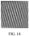
FIG. 14 is a schematic diagram of an image without moire fringes imaged by the fingerprint identification apparatus according to an embodiment of the present application. - Technical solutions in embodiments of the present application will be described hereinafter in conjunction with the accompanying drawings.
- The technical solutions in the embodiments of the present application can be applied to various electronic devices, for example, portable or mobile computing devices such as a smart phone, a notebook computer, a tablet computer and a game device, and other electronic devices such as an electronic database, an automobile and an automated teller machine (Automated Teller Machine, ATM), which is not limited in the embodiments of the present application.
- The technical solutions in the embodiments of the present application can be used for under-screen optical image capturing, for example, under-screen biometric identification or hidden under-screen camera function, and the biometric identification may include other biometric identification in addition to fingerprint identification, for example, living body identification and the like, which is not limited in the embodiments of the present application. In order to facilitate understanding of the technical solution of the embodiment of the present application, under-screen biometric identification technology is first introduced below.
- As an electronic device enters an era of full screen, a biometric capturing area on the front of the electronic device is squeezed by the full screen, and therefore, the under-display (under-display or under-screen) biometric identification technology has gained an increasing attention. The under-screen biometric identification technology refers to mounting a biometric identification module (such as a fingerprint identification module) under a display screen, thereby realizing a biometric identification operation inside a display area of the display screen, without setting a biometric capturing area in an area on the front of an electronic device other than the display area.
- The under-screen biometric identification technology uses light returned from a top surface of a display assembly of a device for fingerprint sensing and other sensing operations. The returned light carries information of an object (e.g., a finger) in contact with the top surface, and a particular optical sensor module located under a display screen is implemented by capturing and detecting the returned light. The optical sensor module may be designed to achieve desired optical imaging by properly configuring an optical element for capturing and detecting a returned light.
-
FIG. 1 and FIG. 2 are schematic views showing anelectronic device 100 to which under-screen biometric identification technology is applicable.FIG. 1 is schematic front view of theelectronic device 100, andFIG. 2 is a partial schematic cross-sectional structural view of theelectronic device 100 shown inFIG. 1 . - As shown in
FIG. 1 and FIG. 2 , theelectronic device 100 may include adisplay screen 120 and abiometric identification module 140; and thedisplay screen 120 has adisplay area 102, and thebiometric identification module 140 is disposed under thedisplay screen 120. - The
display screen 120 may be a self-emitting display screen that employs a self-emitting display unit as a display pixel. For example, thedisplay screen 120 may be an organic light-emitting diode (Organic Light-Emitting Diode, OLED) display screen or a micro light-emitting diode (Micro-LED) display screen. In other alternative embodiments, thedisplay screen 120 may also be a liquid crystal display (Liquid Crystal Display, LCD) screen or other passive light-emitting display screens, which is not limited in the embodiments of the present application. - On the other hand, the
display screen 120 is specifically a touch display screen, which may not only display a screen but also detect a touch or press operation of a user, thereby providing the user with a human-machine interaction interface. For example, in an embodiment, theelectronic device 100 may include a touch sensor, and the touch sensor may be specifically a touch panel (Touch Panel, TP), which may be disposed on a surface of thedisplay screen 120, or may be partially integrated or entirely integrated into an interior of thedisplay screen 120 to form a touch display screen. - The
biometric identification module 140 may be specifically an optical biometric identification module, such as an optical fingerprint module, which is mainly used for capturing biometric information (such as fingerprint image information) of a user. In the embodiments of the present application, thebiometric identification module 140 may be disposed at least in a partial area under thedisplay screen 120 such that the biometric capturing area (or sensing area) 130 of the under-screenbiometric identification module 140 is at least partially located in thedisplay area 102 of thedisplay screen 120. - As an embodiment, the
biometric identification module 140 may include an optical image capturing apparatus, the optical image capturing apparatus may include a plurality of optical image capturing units, and the optical image capturing unit may specifically include a photo detector or a photoelectric sensor. - Alternatively, the optical image capturing apparatus of the
biometric identification module 140 may include a photo detector (Photo detector) array (or referred to as a photoelectric detector array, a photoelectric sensor array), including a plurality of photo detectors/photoelectric sensors distributed in an array. - Alternatively, the optical image capturing apparatus of the
biometric identification module 140 may include an optical biometric sensor with an optical sensing array, such as an optical fingerprint sensor; and the optical sensing array includes a plurality of optical sensing units; the optical sensing unit may specifically include a photo detector or a photoelectric sensor, and an area where the optical sensing array is located or an optical sensing range corresponds to thebiometric capturing area 130 of thebiometric identification module 140. - As shown in
FIG. 1 , thebiometric capturing area 130 is located in thedisplay area 102 of thedisplay screen 120. Therefore, when a user needs to unlock theelectronic device 100 or perform other biometric verification, a biometric input operation can be implemented merely by pressing a finger on thebiometric capturing area 130 located on thedisplay screen 120. Since biometric capturing and detection can be implemented inside thedisplay area 102 of thedisplay screen 120, a front surface of theelectronic device 100 in the above structure does not need to reserve space to set a fingerprint button (such as a Home button), and a full screen solution can be adopted. Therefore, thedisplay area 102 of thedisplay screen 120 can be substantially extended to the entire front surface of theelectronic device 100. - In the embodiment of the present application, the
display screen 120 adopting an OLED display screen is taken as an example, a light emitting layer of thedisplay screen 120 has an array of OLED display units distributed in an array, and thebiometric identification module 140 can utilize an OLED display unit (i.e., an OLED light source) of theOLED display screen 120 located in thebiometric capturing area 130 as an excitation light source for biometric detection and identification. Of course, it should be understood that in other alternative implementations, thebiometric identification module 140 may also provide a light signal for biometric detection and identification by adopting an internal light source or an external light source. In this case, the optical image capturing unit can be applied not only to a self-emitting display screen such as an OLED display screen, but also to a non-self-emitting display screen such as a liquid crystal display screen or other passive light-emitting display screens. - When a finger touches, presses, or approaches (collectively referred to as pressing for convenience of description) the
biometric capturing area 130, light emitted by the display unit of thebiometric capturing area 130 is reflected by the finger to form reflected light. The reflected light may carry biometric information of a user's finger. For example, after the light is reflected by a fingerprint on the surface of the user's finger, since the reflected light of a fingerprint ridge is different from that of a fingerprint valley, the reflected light carries fingerprint information of the user. The reflected light is returned to thedisplay screen 120, received by a photo detector array of thebiometric identification module 140 underneath, and converted into a corresponding electrical signal, i.e., a biometric detection signal. Theelectronic device 100 can obtain biometric information of the user based on the biometric detection signal, and can further perform biometric matching verification, thereby completing identity verification of the current user so as to confirm whether the user has permission to perform a corresponding operation on theelectronic device 100. - In other alternative embodiments, the
biometric identification module 140 may also be disposed in an entire area under thedisplay screen 120 so as to extend thebiometric capturing area 130 to theentire display area 102 of thedisplay screen 120, thereby implementing full screen biometric identification. - It should be understood that in a specific implementation, the
electronic device 100 further includes aprotective cover 110, thecover 110 may be specifically a transparent cover such as a glass cover or a sapphire cover which is located on thedisplay screen 120 and covers a front surface of theelectronic device 100, and the surface of theprotective cover 110 may also be provided with a protective layer. Therefore, in an embodiment of the present application, the so-called pressing finger against thedisplay screen 120 actually refers to pressing the finger against thecover 110 on thedisplay screen 120 or a surface of the protective layer covering thecover 110. - On the other hand, a
circuit board 150, such as a flexible printed circuit (Flexible Printed Circuit, FPC) may further be disposed under thebiometric identification module 140. Thebiometric identification module 140 may be soldered to thecircuit board 150 through a pad, and achieve electrical interconnection and signal transmission with other peripheral circuits or other elements of theelectronic device 100 through thecircuit board 150. For example, thebiometric identification module 140 may receive a control signal of a processing unit of theelectronic device 100 through thecircuit board 150, and may also output the biometric detection signal to the processing unit, a control unit or the like of theelectronic device 100 through thecircuit board 150. -
FIG. 3 is a schematic block diagram of a fingerprint identification system. - As shown in
FIG. 3 , theelectronic device 100 may be composed of a plurality of laminated layers. - Specifically, from top to bottom the electronic device may include a finger for image capturing, an organic light-emitting diode (Organic Light-Emitting Diode, OLED) display screen, an optical imaging component, and a fingerprint sensor (sensor). Wherein the display screen may include a light-emitting pixel array; the light-emitting pixel array includes a plurality of light-emitting pixel units, and the light-emitting pixel units may specifically include a light-emitting diode, such as an organic light-emitting diode (Organic Light-Emitting Diode, OLED). The fingerprint sensor includes the optical sensing array, the optical sensing array includes a plurality of optical sensing units, and the optical sensing units may specifically include a photo detector or a photoelectric sensor.
- In the fingerprint identification system shown in
FIG. 3 , since the structural form of the OLED display screen is similar to the structural form of the optical sensor, the optical sensor will generate moire fringes when imaging based on light transmitting through the display screen, thereby affecting fingerprint identification performance. - Specifically, the image captured by the fingerprint sensor may include a fingerprint image and a sampling pattern of the light-emitting pixel unit, and the sampling pattern of the light-emitting pixel unit may interfere with the fingerprint image at a constant angle and frequency, making the human eye unable to distinguish the fingerprint image and the sampling pattern of the light-emitting pixel unit.
FIG. 4 is an example of an image with moire fringes captured by the fingerprint sensor. - An embodiment of the present application provides a fingerprint identification apparatus, which can effectively solve the interference problem of moire fringes in the imaging system, thereby improving fingerprint identification performance.
- The fingerprint identification apparatus may include:
a fingerprint sensor; and the fingerprint sensor including an optical sensing array, and a spatial period N of the optical sensing array satisfies N<M/2K, wherein M is a spatial period of a light-emitting pixel array, and K is a zoom ratio between an image displayed in a sensing area of the fingerprint sensor and an image captured in the sensing area by the fingerprint sensor. - Further, after deforming N<M/2K, M/K>2N can be obtained.
- Wherein M/K is a period of the sampling pattern of the light-emitting pixel unit in the image captured by the fingerprint sensor.
- That is, in the image captured by the fingerprint sensor, even if the image captured by the fingerprint sensor includes a fingerprint image and a sampling pattern of the light-emitting pixel unit, the period of the sampling pattern of the light-emitting pixel unit is twice greater than that of the fingerprint image.
- Furthermore, after deforming M/K>2N, 1/2f1>1/f2 can be obtained.
- Wherein f1 is a capturing frequency of the sampling pattern of the light-emitting pixel unit, and f2 is a capturing frequency of the fingerprint image.
- That is to say, in the image captured by the fingerprint sensor, even if the image captured by the fingerprint sensor includes a fingerprint image and a sampling pattern of the light-emitting pixel unit, the capturing frequency of the fingerprint image is also twice greater than that of the sampling pattern of the light-emitting pixel unit.
- In an embodiment of the present application, the fingerprint sensor samples the fingerprint image signal from a signal emitted by the light-emitting pixel unit; according to the sampling principle, the sampling frequency of the fingerprint image is twice greater than that of the sampling pattern of the light-emitting pixel unit, and thus avoiding under-sampling of the fingerprint image in the image captured by the fingerprint sensor, thereby avoiding moire fringes in the image captured by the fingerprint sensor, and improving fingerprint identification performance.
- In summary, in the technical solution of the embodiment of the presented application, by clarifying the relationship between the spatial period of the light-emitting pixel array in the display screen and the spatial period of the optical sensing array in the fingerprint sensor, it can avoid the sensor from generating moire fringes when imaging based on light received by transmitting through the display screen, thereby improving fingerprint identification performance.
- In some embodiments of the present application, the fingerprint identification apparatus further includes:
an optical component, the optical component disposed above the optical sensing array, and configured to guide a light signal emitted by the light-emitting pixel array and reflected from a human finger to the optical sensing array. - How to satisfy N<M/2K is described in detail below.
- In an embodiment of the present application, an optical sensing array in a fingerprint sensor can be configured to adjust a spatial period of the optical sensing array, so that N<M/2K.
-
FIG. 5 is a schematic block diagram of an optical sensing array of a fingerprint sensor according to an embodiment of the present application. - As shown in
FIG. 5 , a space period N of the optical sensing array is equal to the sum of a size a of an optical sensing unit in the optical sensing array and a distance s between two adjacent optical sensing units. - In some embodiments of the present application, the optical sensing array may be configured to reduce the size of the optical sensing unit in the optical sensing array, so that N<M/2K. In other embodiments of the present application, the optical sensing array may be configured to reduce the distance between the two adjacent optical sensing units in the optical sensing array, so that N<M/2K.
- As shown in
FIG. 5 , assuming that a spatial period N of a first optical sensing array is equal to 5 um, K=6.6, and M=65 um, then the relationship of M, N and K does not satisfy N<M/2K. That is to say, the image captured by the fingerprint sensor will appear moire fringes. - In the embodiment of the present application, a+s<M/2K=4.925 can be satisfied to further ensure N<M/2K.
- For example, based on maintaining the size a of the optical sensing unit in the optical sensing array, a second optical sensing array shown in
FIG. 5 may reduce the distance s between the two adjacent optical sensing units, so that N<M/2K. For example, the distance s between the two adjacent optical sensing units is reduced, so that a+s<4.925. - For another example, based on maintaining the distance s between the two adjacent optical sensing units, a third optical sensing array shown in
FIG. 5 may reduce the size a of the optical sensing unit in the optical sensing array, so that N<M/2K. For example, the size a of the optical sensing unit in the optical sensing array is reduced, so that a+s<4.925. - For another example, a fourth optical sensing array shown in
FIG. 5 can simultaneously reduce the distance s between the two adjacent optical sensing units and the size a of the optical sensing unit in the optical sensing array, so that N<M/2K. For example, the distance s between the two adjacent optical sensing units and the size a of the optical sensing unit in the optical sensing array are simultaneously reduced, so that a+s<4.925. - It should be understood that
FIG. 5 is only an example of the embodiment of the present application and should not be understood as limitation on the present application. For example, the optical sensing unit shown inFIG. 5 may further be designed into other shapes. For example, the optical sensing unit may be a rectangular, circular, or elliptical optical sensing unit. For another example, the optical sensing array shown inFIG. 5 may further include a plurality of and/or a plurality of lines of optical sensing units. For another example, the optical sensing array shown inFIG. 5 can further be designed into other array shapes. For example, a circular array. - In other alternative embodiments, the spatial period of the optical sensing array may refer to a distance between centers of the two adjacent optical sensing units in the optical sensing array.
- When the optical sensing unit is of an irregular shape, or the two adjacent optical sensing units are different, the space period of the optical sensing array may be greater than or smaller than the sum of the size of the optical sensing unit and the distance between the two adjacent optical sensing units. However, the optical sensing array may still be configured to reduce the size of the optical sensing unit in the optical sensing array and/or to reduce the distance between the two adjacent optical sensing units in the optical sensing array, so that N<M/2K. This is not limited in the embodiment of the present application.
- In an embodiment of the present application, the K may be reduced, so that N<M/2K.
- Alternatively, the optical component may be configured to reduce the K, so that N<M/2K.
- Wherein as shown in
FIG. 3 , the optical component is disposed above the optical sensing array, and configured to guide a light signal emitted by the light-emitting pixel array and reflected from a human finger to the optical sensing array. - Optionally, in some embodiments of the present application, the optical component includes:
a lens, wherein the K is a zoom ratio of the lens. -
FIG. 6 is a schematic view of an imaging principle of the optical component, when the optical component in the fingerprint identification apparatus according to an embodiment of the present application is a lens. - As shown in
FIG. 6 , the lens is configured to guide the light signal carrying information of an object (for example, a human finger) to the fingerprint sensor, so that the fingerprint sensor performs optical imaging based on the light signal. In the embodiment of the present application, the K is the zoom ratio between the object and the image. For example, the K is a ratio between an object distance of the lens and an image distance of the lens. - For example, suppose that parameter configuration of the electronic device is as follows:
M=65um, P=2.64, Q=0.4, K=P/Q=6.6, and N=5um. - Then the relationship of M, N and K does not satisfy N<M/2K. That is to say, the image captured by the fingerprint sensor will appear moire fringes.
- In the embodiment of the present application, P/Q<M/2N can be satisfied to further ensure N<M/2K.
- Wherein the P is the object distance of the lens, and the Q is the image distance of the lens.
- Specifically, the lens is configured to reduce the object distance P of the lens, so that N<M/2K. In other embodiments of the present application, the lens is configured to increase the image distance Q of the lens, so that N<M/2K.
- For example, based on maintaining the object distance P of the lens, the lens shown in
FIG. 6 increases the image distance Q of the lens, so that N<M/2K. For example, the image distance Q of the lens is increased, so that P/Q<6.5. - For another example, based on maintaining the image distance Q of the lens, the lens shown in
FIG. 6 reduces the object distance P of the lens, so that N<M/2K. For example, the image distance Q of the lens is increased, so that P/Q<6.5. - For another example, based on reducing the object distance P of the lens, the lens shown in
FIG. 6 may simultaneously increase the image distance Q of the lens, so that N<M/2K. For example, based on reducing the object distance P of the lens, the lens may simultaneously increase the image distance Q of the lens, so that P/Q<6.5. - It should be understood that the optical component shown in
FIG. 6 is only an example of the embodiment of the present application and should not be understood as limitation on the present application. For example, in other alternative embodiments, the optical component may also be an optical collimator; and in this case, K=1. - In the embodiment of the present application, a spatial period of a light-emitting pixel array in a display screen can be set or adjusted, so that N<M/2K. Wherein the light-emitting pixel unit in the light-emitting pixel array serve as an excitation light source of an optical sensing unit of an optical sensing array in a fingerprint sensor.
-
FIG. 7 is a schematic block diagram of a light-emitting pixel array in a display screen according to an embodiment of the present application. - As shown in
FIG. 7 , a space period M of the light-emitting pixel array is equal to the sum of a size b of a light-emitting pixel unit in the light-emitting pixel array and a distance t between two adjacent light-emitting pixel units. - In some embodiments of the present application, the light-emitting pixel array may be configured to increase the size of the light-emitting pixel unit in the light-emitting pixel array, so that N<M/2K. In other embodiments of the present application, the light-emitting pixel array is configured to increase the distance between the two adjacent light-emitting pixel units in the light-emitting pixel array, so that N<M/2K.
- As shown in
FIG. 7 , assuming that a spatial period M of a first light-emitting pixel array is equal to 65 um, K=6.6, and N=5 um, then the relationship of M, N and K does not satisfy N<M/2K. That is to say, the image captured by the fingerprint sensor will appear moire fringes. - In the embodiment of the present application, b+t>2∗N∗K=66 can be satisfied to further ensure N<M/2K.
- As shown in
FIG. 7 , suppose that N<M/2K is not satisfied. - For example, based on maintaining the size b of the light-emitting pixel unit in the light-emitting pixel array, a second light-emitting pixel array shown in
FIG. 7 may increase the distance t between the two adjacent light-emitting pixel units, so that N<M/2K. For example, the distance t between the two adjacent light-emitting pixel units is increased, so that b+t<66. - For another example, based on maintaining the distance t between the two adjacent light-emitting pixel units, a third light-emitting pixel array shown in
FIG. 7 may increase the size b of the light-emitting pixel unit in the light-emitting pixel array, so that N<M/2K. For example, the size b of the light-emitting pixel unit in the light-emitting pixel array is increased, so that b+t> 66. - For another example, a fourth light-emitting pixel array shown in
FIG. 7 may simultaneously increase the distance t between the two adjacent light-emitting pixel units and the size b of the light-emitting pixel unit in the light-emitting pixel array, so that N<M/2K. For example, the distance t between the two adjacent light-emitting pixel units and the size b of the light-emitting pixel unit in the light-emitting pixel array are simultaneously increased, so that b+t>66. - It should be understood that
FIG. 7 is only an example of the embodiment of the present application and should not be understood as limitation on the present application. For example, the light-emitting pixel unit shown inFIG. 7 may further be designed into other shapes. For example, the light-emitting pixel unit may be a rectangular, circular, or elliptical light-emitting pixel unit. For another example, the light-emitting pixel array shown inFIG. 7 may further include a plurality of and/or a plurality of lines of light-emitting pixel units. For another example, the light-emitting pixel array shown inFIG. 7 can further be designed into other array shapes. For example, a circular array. - In other alternative embodiments, the spatial period of the light-emitting pixel array may refer to a distance between centers of two adjacent light-emitting pixel units in the light-emitting pixel array.
- When the light-emitting pixel unit is of an irregular shape, or the two adjacent light-emitting pixel units are different, the space period of the light-emitting pixel array may be greater than or smaller than the sum of the size of the light-emitting pixel unit and the distance between the two adjacent light-emitting pixel units. However, the light-emitting pixel array can still be configured to increase the size of the light-emitting pixel unit in the light-emitting pixel array and/or to increase the distance between the two adjacent light-emitting pixel units in the light-emitting pixel array, so that N<M/2K. This is not limited in the embodiment of the present application.
- In an embodiment of the present application, a light-emitting pixel unit in the light-emitting pixel array can be configured to emit different light signals to equivalently increase a spatial period of the light-emitting pixel array.
- Specifically, a space period M of the light-emitting pixel array includes a plurality of light-emitting pixel units; when the fingerprint identification apparatus is configured for fingerprint identification, part of the light-emitting pixel units in the plurality of light-emitting pixel units serve as an excitation light source for the fingerprint identification apparatus, and the other part of the light-emitting pixel units in the plurality of light-emitting pixel units emits light signals that are different from those emitted by light-emitting pixel units serving as the excitation light source for the fingerprint identification apparatus.
- For example, the other part of the light-emitting pixel units in the plurality of light-emitting pixel units are configured to emit a striped light spot.
-
FIG. 8 is another schematic block diagram of a light-emitting pixel array in a display screen according to an embodiment of the present application. - As shown in
FIG. 8 , assuming that the spatial period M of a first light-emitting pixel array is equal to 65um, K=6.6, and N=5um, then the relationship of M, N and K does not satisfy N<M/2K. That is to say, the image captured by the fingerprint sensor will appear moire fringes. - In the embodiment of the present application, M>=66 can be satisfied to ensure N<M/2K.
- As shown in
FIG. 8 , the light-emitting pixel units configured to emit a striped light spot in a fifth light-emitting pixel array and the light-emitting pixel unit serving as the excitation light source for the fingerprint identification apparatus are arranged at intervals. That is, a spatial period of the fifth light-emitting pixel array can be equivalent to 130, so that N<M/2K. - It should be understood that
FIG. 8 is only an example of the embodiment of the present application and should not be understood as limitation on the present application. - For example, in other alternative embodiments, a plurality of light-emitting pixel units serving to emit the striped light spot may be further disposed between two adjacent light-emitting pixel units serving as the excitation light source for the fingerprint identification apparatus in the light-emitting pixel unit shown in
FIG. 8 . - For another example, in other alternative embodiments, a plurality of light-emitting pixel units serving as the excitation light source for the fingerprint identification apparatus may be further disposed between two adjacent light-emitting pixel units serving to emit the striped light spot in the light-emitting pixel unit shown in
FIG. 8 . - For another example, in other alternative embodiments, the light-emitting pixel units serving to emit the striped light spot in the light-emitting pixel unit shown in
FIG. 8 may be further configured to emit light signals of other shapes or spectral ranges. - Since a fingerprint image and a sampling pattern of a light-emitting pixel unit included in an image captured by the fingerprint sensor are imaged on the same plane, by clarifying the relationship between a spatial period M of a light-emitting pixel array in a display screen and an equivalent spatial period N1 projected by a spatial period N of an optical sensing array in the fingerprint sensor on the plane, it can also avoid the sensor from generating moire fringes when imaging based on light received by transmitting through the display screen, thereby improving fingerprint identification performance.
- In the embodiment of the present application, the positional relationship between the light-emitting pixel array in the display screen and the optical sensing array in the fingerprint sensor can be set, so that the relationship of the equivalent space period N1, M, and K of the optical sensing array satisfies N1<M/2K.
- For example, suppose that parameter configuration of the electronic device is as follows:
M=65um, K=6.6, and N=5um. - It can be seen that when the fingerprint sensor is not rotated relative to the display screen, the relationship of M, N and K does not satisfy N<M/2K. That is to say, the image captured by the fingerprint sensor will appear moire fringes.
-
FIG. 9 is a schematic front view of a structure formed by rotating the fingerprint sensor relative to the display screen by a certain angle in theelectronic device 200 according to an embodiment of the present application.FIG. 10 is a schematic diagram of a positional relationship between two adjacent optical sensing units shown inFIG. 9 . - As shown in
FIG. 9 , the electronic device includes aprotective cover 210, a display screen may be disposed under theprotective cover 210, and afingerprint sensor 231 may be disposed under the display screen. A fingerprint capturing area of thefingerprint sensor 231 is located in adisplay area 202 of the display screen. Thefingerprint sensor 231 is rotated at a certain angle relative to the display screen. - Further, as shown in
FIG. 10 , assuming that a direction of a row of the light-emitting pixel array in the display screen is the lateral direction of theprotective cover 210, a spatial period of the light-emitting pixel array projected on the row of the light-emitting pixel array has a equivalent period cycle N1 of: N∗cosθ um. - Assuming that the angle θ shown in
FIG. 9 is 15°, then N1=5∗cos(15°) um. - It can be seen that 5∗cos(π/6)<65/(2∗6.6), that is, the relationship of M, N1 and K satisfies N1<M/2K.
- It should be understood that
FIG. 9 is only an example of the embodiment of the present application and should not be understood as limitation on the present application. For example, the rotation method of thefingerprint sensor 231 is not limited in the embodiment of the present application. - For example, as shown in
FIG. 9 , thefingerprint sensor 231 may be rotated counterclockwise by a certain angle θ. - For another example, the
fingerprint sensor 232 shown inFIG. 11 may be rotated clockwise by a certain angle θ. - For another example, the
fingerprint sensor 233 shown inFIG. 12 may be rotated counterclockwise or clockwise by a certain angle, so that a row of the optical sensing array in thefingerprint sensor 233 and the row of the light-emitting pixel array in the display screen form an angle θ, and thefingerprint sensor 233 is tilted to the left. - For another example, the
fingerprint sensor 234 shown inFIG. 13 can be rotated counterclockwise or clockwise by a certain angle, so that the row of the optical sensing array in thefingerprint sensor 234 and the row of the light-emitting pixel array in the display screen form an angle θ, and thefingerprint sensor 234 is tilted to the right. - For another example, in other alternative embodiments, the fingerprint sensor can also be rotated by a certain angle in the direction perpendicular to the display screen, so that N1<M/2K.
- It should be understood that a specific structure of the fingerprint sensor in
FIG. 9 to FIG. 13 may refer to thebiometric identification module 140 shown inFIG. 1 and FIG. 2 , and the relevant description of theprotective cover 210 and thedisplay area 202 may refer to theprotective cover 110 and thedisplay area 102 shown inFIG. 1 and FIG. 2 , respectively, which is not repeatedly described herein in order to avoid repetition. - It should be noted that only when N<M/2K, by setting an angle between the light-emitting pixel array in the display screen and the optical sensing array in the fingerprint sensor, an area occupied by the fingerprint sensor in the electronic device may increase, thereby affecting further optimization of electronic device performance. For example, as shown in
FIG. 9 , a projected area of the rotated fingerprint sensor on theprotective cover 210 of the electronic device is the product of h and w, and is larger than a projected area of thefingerprint sensor 231 on theprotective cover 210. - Therefore, in order to avoid the area occupied by the fingerprint sensor in the electronic device, a method of combining the above multiple embodiments can be applied to make N<M/2K.
- It should be understood that the combination method of the above 5 embodiments is not specifically limited in the embodiment of the present application.
- For example, the moire fringe can be completely eliminated through one or more implementation manners described in the above 5 embodiments. For example, as shown in
FIG. 14 , the fingerprint sensor of the embodiment of the present application can effectively eliminate the moire fringes when imaging based on light received by transmitting through the display screen, thereby improving fingerprint identification performance. - For another example, if limited by factors such as production and manufacturing, one or more implementation methods described in the above 5 embodiments may be used to appropriately adjust some parameters within a certain range, thereby reducing the moire fringes to a certain extent.
- It should also be noted that the embodiment of the present application aims to clarify the relationship of M, N and K (i.e., N<M/2K), to weaken or eliminate the moire fringes. However, the embodiment of the present application does not limit specific values of M, N and K.
- For example, a range of a space period N of the optical sensing array may be 1um-20um. Preferably, the N may be 3.6um, 5um, 7.2um, 12.5um, etc.
- For another example, a range of a space period M of the light-emitting pixel array may be 40um-120um. Preferably, the N may be 65um, 80um, 85um, etc.
- For another example, a value range of the K may be 1-20. Preferably, the K may be 6.6, etc.
- For another example, a range of the angle may be -15° to 15°. Preferably, the angle may be 10°, 8°, 0°, etc.
- It should be understood that the above parameters are only an example of the embodiment of the present application and should not be understood as limitation on the present application.
- In the several embodiments provided in the present application, it should be understood that, the disclosed fingerprint identification apparatus and electronic device may be implemented in other manners.
- For example, the division of the units or modules or components in the apparatus embodiments described above is only a logic function division, other division modes may be adopted in practice, e.g., multiple units or modules or components may be combined or integrated in another system, or some units or modules or components may be omitted or be not executed.
- For another example, the units/modules/components described as separate/display components may be or may not be physically separated, namely, may be located in one place, or may be distributed on a plurality of units. Part of or all of the units/modules/components here may be selected according to a practical need to achieve the objectives of the embodiments of the present application.
- The above contents are the specific embodiments of the present application only, but the protection scope of the embodiments of present application is not limited thereto, those skilled who are familiar with the art could readily think of variations or substitutions within the technical scope disclosed by the embodiments of the present application, and these variations or substitutions shall fall within the protection scope of the embodiments of the present application. Therefore, the protection scope of the embodiments of the present application should be determined with reference to the protection scope of the claims.
Claims (23)
- A fingerprint identification apparatus, comprising:a fingerprint sensor; andthe fingerprint sensor comprising an optical sensing array, and a spatial period N of the optical sensing array satisfies N<M/2K;wherein M is a spatial period of a light-emitting pixel array, and K is a zoom ratio between an image displayed in a sensing area of the fingerprint sensor and an image captured in the sensing area by the fingerprint sensor.
- The fingerprint identification apparatus according to claim 1, wherein a range of the space period of the optical sensing array is 1um-20um.
- The fingerprint identification apparatus according to claim 2, wherein the space period of the optical sensing array is 5.
- The fingerprint identification apparatus according to any one of claims 1 to 3, wherein the space period of the optical sensing array is equal to the sum of a size of an optical sensing unit in the optical sensing array and a distance between two adjacent optical sensing units.
- The fingerprint identification apparatus according to claim 4, wherein the optical sensing array is configured to reduce the size of the optical sensing unit in the optical sensing array, so that N<M/2K.
- The fingerprint identification apparatus according to claim 4, wherein the optical sensing array is configured to reduce the distance between the two adjacent optical sensing units in the optical sensing array, so that N<M/2K.
- The fingerprint identification apparatus according to any one of claims 1 to 6, wherein the fingerprint identification apparatus further comprises:the optical component; andthe optical component disposed above the optical sensing array, and configured to guide a light signal emitted by the light-emitting pixel array and reflected from a human finger to the optical sensing array.
- The fingerprint identification apparatus according to claim 7, wherein a value range of the K is 1-20.
- The fingerprint identification apparatus according to claim 7, wherein the optical component is configured to reduce the K, so that N<M/2K.
- The fingerprint identification apparatus according to claim 7, wherein the optical component comprises:
a lens, wherein the K is a ratio between an object distance of the lens and an image distance of the lens. - The fingerprint identification apparatus according to claim 10, wherein the lens is configured to reduce the object distance of the lens, so that N<M/2K.
- The fingerprint identification apparatus according to claim 10, wherein the lens is configured to increase the image distance of the lens, so that N<M/2K.
- The fingerprint identification apparatus according to any one of claims 1 to 12, wherein a row of the optical sensing array has an angel with a row of the light-emitting pixel array.
- The fingerprint identification apparatus according to any one of claims 1 to 13, wherein a line of the optical sensing array has an angel with a row of the light-emitting pixel array.
- The fingerprint identification apparatus according to claim 13 or 14, wherein a range of the angle is -15° to 15°.
- An electronic device, comprising:the fingerprint identification apparatus according to any one of claims 1 to 15; anda light-emitting pixel array in the display screen; an optical sensing array in the fingerprint identification apparatus configured to receive a light signal emitted by the light-emitting pixel array and formed after being reflected from a human finger, the light signal being used for fingerprint identification.
- The electronic device according to claim 16, wherein a range of a space period of the light-emitting pixel array is 40um-120um.
- The electronic device according to claim 16 or 17, wherein the space period of the light-emitting pixel array comprises a plurality of light-emitting pixel units, and part of the light-emitting pixel units in the plurality of light-emitting pixel units serve as an excitation light source for the fingerprint identification apparatus.
- The electronic device according to claim 18, wherein the other part of the light-emitting pixel units in the plurality of light-emitting pixel units are configured to emit a striped light spot.
- The electronic device according to any one of claims 16 to 19, wherein the space period of the light-emitting pixel is equal to the sum of a size of a light-emitting pixel unit in the light-emitting pixel array and a distance between two adjacent light-emitting pixel units.
- The electronic device according to claim 20, wherein the light-emitting pixel array is configured to increase the size of the light-emitting pixel unit in the light-emitting pixel array, so that N<M/2K.
- The electronic device according to claim 20, wherein the light-emitting pixel array is configured to increase the distance between the two adjacent light-emitting pixel units in the light-emitting pixel array, so that N<M/2K.
- The electronic device according to any one of claims 16 to 22, wherein the display screen is an organic light-emitting diode (OLED) display screen.
Applications Claiming Priority (1)
| Application Number | Priority Date | Filing Date | Title |
|---|---|---|---|
| PCT/CN2018/121261 WO2020118699A1 (en) | 2018-12-14 | 2018-12-14 | Fingerprint recognition apparatus and electronic device |
Publications (3)
| Publication Number | Publication Date |
|---|---|
| EP3796208A1 true EP3796208A1 (en) | 2021-03-24 |
| EP3796208A4 EP3796208A4 (en) | 2021-06-02 |
| EP3796208B1 EP3796208B1 (en) | 2023-03-15 |
Family
ID=66190488
Family Applications (1)
| Application Number | Title | Priority Date | Filing Date |
|---|---|---|---|
| EP18942800.6A Active EP3796208B1 (en) | 2018-12-14 | 2018-12-14 | Fingerprint recognition apparatus and electronic device |
Country Status (4)
| Country | Link |
|---|---|
| US (1) | US11361583B2 (en) |
| EP (1) | EP3796208B1 (en) |
| CN (2) | CN109690567B (en) |
| WO (1) | WO2020118699A1 (en) |
Families Citing this family (16)
| Publication number | Priority date | Publication date | Assignee | Title |
|---|---|---|---|---|
| CN108256409A (en) * | 2017-10-27 | 2018-07-06 | 京东方科技集团股份有限公司 | Display device and its fingerprint identification method |
| CN111325055B (en) * | 2018-12-14 | 2024-03-19 | 上海耕岩智能科技有限公司 | Fingerprint identification method and device, storage medium and terminal |
| CN111382732B (en) * | 2018-12-28 | 2024-01-23 | 京东方科技集团股份有限公司 | Texture recognition device and method of operating the texture recognition device |
| CN111914593A (en) * | 2019-05-08 | 2020-11-10 | 上海耕岩智能科技有限公司 | Image acquisition method and device, storage medium and electronic equipment |
| CN111353405B (en) * | 2019-07-17 | 2023-08-11 | 上海思立微电子科技有限公司 | Fingerprint identification device, fingerprint identification system and electronic equipment |
| WO2021168666A1 (en) * | 2020-02-25 | 2021-09-02 | 深圳市汇顶科技股份有限公司 | Fingerprint identification apparatus and electronic device |
| CN113361298A (en) * | 2020-03-02 | 2021-09-07 | Oppo广东移动通信有限公司 | Electronic device |
| WO2021196441A1 (en) * | 2020-03-30 | 2021-10-07 | 神盾股份有限公司 | Electronic apparatus with fingerprint sensor and high-resolution display that fit each other |
| CN111898415B (en) * | 2020-06-16 | 2023-08-08 | 浙江大学 | Under-screen fingerprint imaging method and device and electronic equipment |
| CN113469131A (en) * | 2020-09-08 | 2021-10-01 | 神盾股份有限公司 | Sensing device using sensing pixels with partial spectral sensing area |
| CN114449230A (en) * | 2020-10-30 | 2022-05-06 | 中兴通讯股份有限公司 | Photographing method, photographing device, terminal and computer-readable storage medium |
| CN115943444A (en) | 2021-01-22 | 2023-04-07 | 京东方科技集团股份有限公司 | Display panel and display device |
| CN115147881A (en) * | 2021-03-31 | 2022-10-04 | 北京小米移动软件有限公司 | Optical fingerprint sensor, optical fingerprint module, display screen and terminal equipment |
| CN116030505A (en) * | 2021-10-22 | 2023-04-28 | 北京与光科技有限公司 | Unlocking device and unlocking method |
| CN114279332B (en) * | 2021-12-27 | 2023-11-03 | 深圳市汇顶科技股份有限公司 | Method and device for positioning sensor under display screen and electronic equipment |
| CN116935453A (en) * | 2023-07-04 | 2023-10-24 | 天津极豪科技有限公司 | Optical fingerprint module and electronic equipment |
Family Cites Families (18)
| Publication number | Priority date | Publication date | Assignee | Title |
|---|---|---|---|---|
| DE69735736T2 (en) * | 1996-01-31 | 2006-11-02 | Canon K.K. | Stereoscopic image display device with broadened field of view |
| JP3758284B2 (en) * | 1997-03-17 | 2006-03-22 | コニカミノルタフォトイメージング株式会社 | Imaging device |
| JP2005321996A (en) * | 2004-05-07 | 2005-11-17 | Pioneer Electronic Corp | Information input device and method |
| US8035711B2 (en) * | 2008-05-22 | 2011-10-11 | Panavision Imaging, Llc | Sub-pixel array optical sensor |
| US9460332B1 (en) * | 2013-09-09 | 2016-10-04 | Apple Inc. | Capacitive fingerprint sensor including an electrostatic lens |
| US9558390B2 (en) | 2014-07-25 | 2017-01-31 | Qualcomm Incorporated | High-resolution electric field sensor in cover glass |
| US9459747B2 (en) | 2014-12-11 | 2016-10-04 | Microsoft Technology Licensing, Llc | Touch display system with reduced moiré patterns |
| CN106155429A (en) * | 2015-03-25 | 2016-11-23 | 联想(北京)有限公司 | Electronic equipment, touch-control parts and method to set up thereof |
| CN108062187A (en) * | 2016-11-07 | 2018-05-22 | 京东方科技集团股份有限公司 | Touch-control structure and preparation method thereof and touch device |
| KR20180067226A (en) * | 2016-12-12 | 2018-06-20 | 삼성전자주식회사 | touch sensor capable of detecting fingerprint, and display device and electronic apparatus including the same |
| CN106709455B (en) * | 2016-12-23 | 2020-06-30 | 张一帆 | Display screen supporting full-screen optical fingerprint sensor and manufacturing method thereof |
| US10311276B2 (en) * | 2017-02-22 | 2019-06-04 | Synaptics Incorporated | Under display optical fingerprint sensor arrangement for mitigating moiré effects |
| CN107247922B (en) * | 2017-05-12 | 2020-04-03 | Oppo广东移动通信有限公司 | Display device and mobile terminal |
| TW201915818A (en) * | 2017-10-05 | 2019-04-16 | 香港商印芯科技股份有限公司 | Optical recognition module |
| CN207833534U (en) * | 2017-11-09 | 2018-09-07 | 深圳市汇顶科技股份有限公司 | Optics module and terminal device |
| CN108323208A (en) * | 2018-02-12 | 2018-07-24 | 深圳市汇顶科技股份有限公司 | Image acquisition method and device |
| CN108885697B (en) * | 2018-06-15 | 2021-11-05 | 深圳市汇顶科技股份有限公司 | Under-screen biometric identification devices and electronic equipment |
| CN209433415U (en) * | 2018-12-14 | 2019-09-24 | 深圳市汇顶科技股份有限公司 | Fingerprint identification device and electronic equipment |
-
2018
- 2018-12-14 WO PCT/CN2018/121261 patent/WO2020118699A1/en not_active Ceased
- 2018-12-14 CN CN201880002833.8A patent/CN109690567B/en active Active
- 2018-12-14 EP EP18942800.6A patent/EP3796208B1/en active Active
- 2018-12-14 CN CN202010936764.7A patent/CN112070018B/en active Active
-
2020
- 2020-12-15 US US17/123,073 patent/US11361583B2/en active Active
Also Published As
| Publication number | Publication date |
|---|---|
| CN109690567B (en) | 2020-10-02 |
| US11361583B2 (en) | 2022-06-14 |
| CN109690567A (en) | 2019-04-26 |
| WO2020118699A1 (en) | 2020-06-18 |
| CN112070018B (en) | 2023-12-01 |
| EP3796208A4 (en) | 2021-06-02 |
| EP3796208B1 (en) | 2023-03-15 |
| US20210103714A1 (en) | 2021-04-08 |
| CN112070018A (en) | 2020-12-11 |
Similar Documents
| Publication | Publication Date | Title |
|---|---|---|
| US11361583B2 (en) | Fingerprint identification apparatus and electronic device | |
| US11295110B2 (en) | Under-screen biometric identification apparatus and electronic device | |
| CN109496313B (en) | Fingerprint identification device and electronic equipment | |
| US20200097699A1 (en) | Fingerprint identification apparatus and electronic device | |
| CN110023955B (en) | Optical sensor with substrate filter | |
| CN110770746B (en) | Fingerprint identification device and electronic equipment | |
| EP3842991B1 (en) | Optical fingerprint apparatus and electronic device | |
| EP3640845A1 (en) | Optical image collection unit, optical image collection system and electronic device | |
| US20190129530A1 (en) | Under display biometric sensor | |
| WO2019178793A1 (en) | In-display biometric identification device and electronic device | |
| EP3731135A1 (en) | Method and device for fingerprint recognition, and terminal device | |
| WO2020082375A1 (en) | Compound lens structure, fingerprint recognition apparatus, and electronic device | |
| CN111837132B (en) | Fingerprint detection devices and electronic equipment | |
| CN112860120B (en) | Fingerprint identification device, electronic equipment and ambient light detection method | |
| WO2020168496A1 (en) | Method and apparatus for fingerprint recognition, and terminal device | |
| CN112528953B (en) | Fingerprint identification device, electronic equipment and fingerprint identification method | |
| CN111312793B (en) | Electronic equipment | |
| CN209433415U (en) | Fingerprint identification device and electronic equipment | |
| CN210864756U (en) | Optical fingerprint device and electronic equipment | |
| EP3812955B1 (en) | Fingerprint detection apparatus and electronic device | |
| WO2020073166A1 (en) | Fingerprint recognition method and apparatus, and terminal device | |
| CN210534801U (en) | Fingerprint identification device and electronic equipment | |
| CN110832503A (en) | Optical fingerprint device, electronic apparatus and method of measuring distance | |
| WO2020061748A1 (en) | Optical image capturing device and electronic apparatus | |
| CN210864764U (en) | Fingerprint identification device and electronic equipment |
Legal Events
| Date | Code | Title | Description |
|---|---|---|---|
| STAA | Information on the status of an ep patent application or granted ep patent |
Free format text: STATUS: THE INTERNATIONAL PUBLICATION HAS BEEN MADE |
|
| PUAI | Public reference made under article 153(3) epc to a published international application that has entered the european phase |
Free format text: ORIGINAL CODE: 0009012 |
|
| STAA | Information on the status of an ep patent application or granted ep patent |
Free format text: STATUS: REQUEST FOR EXAMINATION WAS MADE |
|
| 17P | Request for examination filed |
Effective date: 20201217 |
|
| AK | Designated contracting states |
Kind code of ref document: A1 Designated state(s): AL AT BE BG CH CY CZ DE DK EE ES FI FR GB GR HR HU IE IS IT LI LT LU LV MC MK MT NL NO PL PT RO RS SE SI SK SM TR |
|
| AX | Request for extension of the european patent |
Extension state: BA ME |
|
| A4 | Supplementary search report drawn up and despatched |
Effective date: 20210503 |
|
| RIC1 | Information provided on ipc code assigned before grant |
Ipc: G06K 9/00 20060101AFI20210426BHEP |
|
| DAV | Request for validation of the european patent (deleted) | ||
| DAX | Request for extension of the european patent (deleted) | ||
| STAA | Information on the status of an ep patent application or granted ep patent |
Free format text: STATUS: EXAMINATION IS IN PROGRESS |
|
| 17Q | First examination report despatched |
Effective date: 20220609 |
|
| REG | Reference to a national code |
Ref country code: DE Ref legal event code: R079 Ref document number: 602018047390 Country of ref document: DE Free format text: PREVIOUS MAIN CLASS: G06K0009000000 Ipc: G06V0040130000 |
|
| GRAP | Despatch of communication of intention to grant a patent |
Free format text: ORIGINAL CODE: EPIDOSNIGR1 |
|
| STAA | Information on the status of an ep patent application or granted ep patent |
Free format text: STATUS: GRANT OF PATENT IS INTENDED |
|
| RIC1 | Information provided on ipc code assigned before grant |
Ipc: G06V 40/13 20220101AFI20221212BHEP |
|
| GRAS | Grant fee paid |
Free format text: ORIGINAL CODE: EPIDOSNIGR3 |
|
| INTG | Intention to grant announced |
Effective date: 20230111 |
|
| GRAA | (expected) grant |
Free format text: ORIGINAL CODE: 0009210 |
|
| STAA | Information on the status of an ep patent application or granted ep patent |
Free format text: STATUS: THE PATENT HAS BEEN GRANTED |
|
| AK | Designated contracting states |
Kind code of ref document: B1 Designated state(s): AL AT BE BG CH CY CZ DE DK EE ES FI FR GB GR HR HU IE IS IT LI LT LU LV MC MK MT NL NO PL PT RO RS SE SI SK SM TR |
|
| REG | Reference to a national code |
Ref country code: CH Ref legal event code: EP Ref country code: GB Ref legal event code: FG4D |
|
| REG | Reference to a national code |
Ref country code: DE Ref legal event code: R096 Ref document number: 602018047390 Country of ref document: DE |
|
| REG | Reference to a national code |
Ref country code: IE Ref legal event code: FG4D |
|
| REG | Reference to a national code |
Ref country code: AT Ref legal event code: REF Ref document number: 1554444 Country of ref document: AT Kind code of ref document: T Effective date: 20230415 |
|
| REG | Reference to a national code |
Ref country code: LT Ref legal event code: MG9D |
|
| REG | Reference to a national code |
Ref country code: NL Ref legal event code: MP Effective date: 20230315 |
|
| PG25 | Lapsed in a contracting state [announced via postgrant information from national office to epo] |
Ref country code: RS Free format text: LAPSE BECAUSE OF FAILURE TO SUBMIT A TRANSLATION OF THE DESCRIPTION OR TO PAY THE FEE WITHIN THE PRESCRIBED TIME-LIMIT Effective date: 20230315 Ref country code: NO Free format text: LAPSE BECAUSE OF FAILURE TO SUBMIT A TRANSLATION OF THE DESCRIPTION OR TO PAY THE FEE WITHIN THE PRESCRIBED TIME-LIMIT Effective date: 20230615 Ref country code: LV Free format text: LAPSE BECAUSE OF FAILURE TO SUBMIT A TRANSLATION OF THE DESCRIPTION OR TO PAY THE FEE WITHIN THE PRESCRIBED TIME-LIMIT Effective date: 20230315 Ref country code: LT Free format text: LAPSE BECAUSE OF FAILURE TO SUBMIT A TRANSLATION OF THE DESCRIPTION OR TO PAY THE FEE WITHIN THE PRESCRIBED TIME-LIMIT Effective date: 20230315 Ref country code: HR Free format text: LAPSE BECAUSE OF FAILURE TO SUBMIT A TRANSLATION OF THE DESCRIPTION OR TO PAY THE FEE WITHIN THE PRESCRIBED TIME-LIMIT Effective date: 20230315 |
|
| REG | Reference to a national code |
Ref country code: AT Ref legal event code: MK05 Ref document number: 1554444 Country of ref document: AT Kind code of ref document: T Effective date: 20230315 |
|
| PG25 | Lapsed in a contracting state [announced via postgrant information from national office to epo] |
Ref country code: SE Free format text: LAPSE BECAUSE OF FAILURE TO SUBMIT A TRANSLATION OF THE DESCRIPTION OR TO PAY THE FEE WITHIN THE PRESCRIBED TIME-LIMIT Effective date: 20230315 Ref country code: NL Free format text: LAPSE BECAUSE OF FAILURE TO SUBMIT A TRANSLATION OF THE DESCRIPTION OR TO PAY THE FEE WITHIN THE PRESCRIBED TIME-LIMIT Effective date: 20230315 Ref country code: GR Free format text: LAPSE BECAUSE OF FAILURE TO SUBMIT A TRANSLATION OF THE DESCRIPTION OR TO PAY THE FEE WITHIN THE PRESCRIBED TIME-LIMIT Effective date: 20230616 Ref country code: FI Free format text: LAPSE BECAUSE OF FAILURE TO SUBMIT A TRANSLATION OF THE DESCRIPTION OR TO PAY THE FEE WITHIN THE PRESCRIBED TIME-LIMIT Effective date: 20230315 |
|
| PG25 | Lapsed in a contracting state [announced via postgrant information from national office to epo] |
Ref country code: SM Free format text: LAPSE BECAUSE OF FAILURE TO SUBMIT A TRANSLATION OF THE DESCRIPTION OR TO PAY THE FEE WITHIN THE PRESCRIBED TIME-LIMIT Effective date: 20230315 Ref country code: RO Free format text: LAPSE BECAUSE OF FAILURE TO SUBMIT A TRANSLATION OF THE DESCRIPTION OR TO PAY THE FEE WITHIN THE PRESCRIBED TIME-LIMIT Effective date: 20230315 Ref country code: PT Free format text: LAPSE BECAUSE OF FAILURE TO SUBMIT A TRANSLATION OF THE DESCRIPTION OR TO PAY THE FEE WITHIN THE PRESCRIBED TIME-LIMIT Effective date: 20230717 Ref country code: ES Free format text: LAPSE BECAUSE OF FAILURE TO SUBMIT A TRANSLATION OF THE DESCRIPTION OR TO PAY THE FEE WITHIN THE PRESCRIBED TIME-LIMIT Effective date: 20230315 Ref country code: EE Free format text: LAPSE BECAUSE OF FAILURE TO SUBMIT A TRANSLATION OF THE DESCRIPTION OR TO PAY THE FEE WITHIN THE PRESCRIBED TIME-LIMIT Effective date: 20230315 Ref country code: CZ Free format text: LAPSE BECAUSE OF FAILURE TO SUBMIT A TRANSLATION OF THE DESCRIPTION OR TO PAY THE FEE WITHIN THE PRESCRIBED TIME-LIMIT Effective date: 20230315 Ref country code: AT Free format text: LAPSE BECAUSE OF FAILURE TO SUBMIT A TRANSLATION OF THE DESCRIPTION OR TO PAY THE FEE WITHIN THE PRESCRIBED TIME-LIMIT Effective date: 20230315 |
|
| PG25 | Lapsed in a contracting state [announced via postgrant information from national office to epo] |
Ref country code: SK Free format text: LAPSE BECAUSE OF FAILURE TO SUBMIT A TRANSLATION OF THE DESCRIPTION OR TO PAY THE FEE WITHIN THE PRESCRIBED TIME-LIMIT Effective date: 20230315 Ref country code: PL Free format text: LAPSE BECAUSE OF FAILURE TO SUBMIT A TRANSLATION OF THE DESCRIPTION OR TO PAY THE FEE WITHIN THE PRESCRIBED TIME-LIMIT Effective date: 20230315 Ref country code: IS Free format text: LAPSE BECAUSE OF FAILURE TO SUBMIT A TRANSLATION OF THE DESCRIPTION OR TO PAY THE FEE WITHIN THE PRESCRIBED TIME-LIMIT Effective date: 20230715 |
|
| REG | Reference to a national code |
Ref country code: DE Ref legal event code: R097 Ref document number: 602018047390 Country of ref document: DE |
|
| PLBE | No opposition filed within time limit |
Free format text: ORIGINAL CODE: 0009261 |
|
| STAA | Information on the status of an ep patent application or granted ep patent |
Free format text: STATUS: NO OPPOSITION FILED WITHIN TIME LIMIT |
|
| PG25 | Lapsed in a contracting state [announced via postgrant information from national office to epo] |
Ref country code: SI Free format text: LAPSE BECAUSE OF FAILURE TO SUBMIT A TRANSLATION OF THE DESCRIPTION OR TO PAY THE FEE WITHIN THE PRESCRIBED TIME-LIMIT Effective date: 20230315 Ref country code: DK Free format text: LAPSE BECAUSE OF FAILURE TO SUBMIT A TRANSLATION OF THE DESCRIPTION OR TO PAY THE FEE WITHIN THE PRESCRIBED TIME-LIMIT Effective date: 20230315 |
|
| 26N | No opposition filed |
Effective date: 20231218 |
|
| PG25 | Lapsed in a contracting state [announced via postgrant information from national office to epo] |
Ref country code: IT Free format text: LAPSE BECAUSE OF FAILURE TO SUBMIT A TRANSLATION OF THE DESCRIPTION OR TO PAY THE FEE WITHIN THE PRESCRIBED TIME-LIMIT Effective date: 20230315 |
|
| REG | Reference to a national code |
Ref country code: CH Ref legal event code: PL |
|
| PG25 | Lapsed in a contracting state [announced via postgrant information from national office to epo] |
Ref country code: LU Free format text: LAPSE BECAUSE OF NON-PAYMENT OF DUE FEES Effective date: 20231214 |
|
| PG25 | Lapsed in a contracting state [announced via postgrant information from national office to epo] |
Ref country code: MC Free format text: LAPSE BECAUSE OF FAILURE TO SUBMIT A TRANSLATION OF THE DESCRIPTION OR TO PAY THE FEE WITHIN THE PRESCRIBED TIME-LIMIT Effective date: 20230315 |
|
| GBPC | Gb: european patent ceased through non-payment of renewal fee |
Effective date: 20231214 |
|
| REG | Reference to a national code |
Ref country code: BE Ref legal event code: MM Effective date: 20231231 |
|
| PG25 | Lapsed in a contracting state [announced via postgrant information from national office to epo] |
Ref country code: MC Free format text: LAPSE BECAUSE OF FAILURE TO SUBMIT A TRANSLATION OF THE DESCRIPTION OR TO PAY THE FEE WITHIN THE PRESCRIBED TIME-LIMIT Effective date: 20230315 Ref country code: LU Free format text: LAPSE BECAUSE OF NON-PAYMENT OF DUE FEES Effective date: 20231214 |
|
| REG | Reference to a national code |
Ref country code: IE Ref legal event code: MM4A |
|
| PG25 | Lapsed in a contracting state [announced via postgrant information from national office to epo] |
Ref country code: IE Free format text: LAPSE BECAUSE OF NON-PAYMENT OF DUE FEES Effective date: 20231214 |
|
| PG25 | Lapsed in a contracting state [announced via postgrant information from national office to epo] |
Ref country code: GB Free format text: LAPSE BECAUSE OF NON-PAYMENT OF DUE FEES Effective date: 20231214 |
|
| PG25 | Lapsed in a contracting state [announced via postgrant information from national office to epo] |
Ref country code: BE Free format text: LAPSE BECAUSE OF NON-PAYMENT OF DUE FEES Effective date: 20231231 |
|
| PG25 | Lapsed in a contracting state [announced via postgrant information from national office to epo] |
Ref country code: FR Free format text: LAPSE BECAUSE OF NON-PAYMENT OF DUE FEES Effective date: 20231231 |
|
| PG25 | Lapsed in a contracting state [announced via postgrant information from national office to epo] |
Ref country code: CH Free format text: LAPSE BECAUSE OF NON-PAYMENT OF DUE FEES Effective date: 20231231 |
|
| PG25 | Lapsed in a contracting state [announced via postgrant information from national office to epo] |
Ref country code: IE Free format text: LAPSE BECAUSE OF NON-PAYMENT OF DUE FEES Effective date: 20231214 Ref country code: GB Free format text: LAPSE BECAUSE OF NON-PAYMENT OF DUE FEES Effective date: 20231214 Ref country code: FR Free format text: LAPSE BECAUSE OF NON-PAYMENT OF DUE FEES Effective date: 20231231 Ref country code: CH Free format text: LAPSE BECAUSE OF NON-PAYMENT OF DUE FEES Effective date: 20231231 Ref country code: BE Free format text: LAPSE BECAUSE OF NON-PAYMENT OF DUE FEES Effective date: 20231231 |
|
| PG25 | Lapsed in a contracting state [announced via postgrant information from national office to epo] |
Ref country code: BG Free format text: LAPSE BECAUSE OF FAILURE TO SUBMIT A TRANSLATION OF THE DESCRIPTION OR TO PAY THE FEE WITHIN THE PRESCRIBED TIME-LIMIT Effective date: 20230315 |
|
| PG25 | Lapsed in a contracting state [announced via postgrant information from national office to epo] |
Ref country code: BG Free format text: LAPSE BECAUSE OF FAILURE TO SUBMIT A TRANSLATION OF THE DESCRIPTION OR TO PAY THE FEE WITHIN THE PRESCRIBED TIME-LIMIT Effective date: 20230315 |
|
| PG25 | Lapsed in a contracting state [announced via postgrant information from national office to epo] |
Ref country code: CY Free format text: LAPSE BECAUSE OF FAILURE TO SUBMIT A TRANSLATION OF THE DESCRIPTION OR TO PAY THE FEE WITHIN THE PRESCRIBED TIME-LIMIT; INVALID AB INITIO Effective date: 20181214 |
|
| PG25 | Lapsed in a contracting state [announced via postgrant information from national office to epo] |
Ref country code: HU Free format text: LAPSE BECAUSE OF FAILURE TO SUBMIT A TRANSLATION OF THE DESCRIPTION OR TO PAY THE FEE WITHIN THE PRESCRIBED TIME-LIMIT; INVALID AB INITIO Effective date: 20181214 |
|
| PG25 | Lapsed in a contracting state [announced via postgrant information from national office to epo] |
Ref country code: TR Free format text: LAPSE BECAUSE OF FAILURE TO SUBMIT A TRANSLATION OF THE DESCRIPTION OR TO PAY THE FEE WITHIN THE PRESCRIBED TIME-LIMIT Effective date: 20230315 |
|
| PGFP | Annual fee paid to national office [announced via postgrant information from national office to epo] |
Ref country code: DE Payment date: 20251210 Year of fee payment: 8 |