EP3796077A1 - Array substrate, display panel, and display device - Google Patents
Array substrate, display panel, and display device Download PDFInfo
- Publication number
- EP3796077A1 EP3796077A1 EP19804564.3A EP19804564A EP3796077A1 EP 3796077 A1 EP3796077 A1 EP 3796077A1 EP 19804564 A EP19804564 A EP 19804564A EP 3796077 A1 EP3796077 A1 EP 3796077A1
- Authority
- EP
- European Patent Office
- Prior art keywords
- connection portion
- signal line
- array substrate
- via holes
- substrate according
- Prior art date
- Legal status (The legal status is an assumption and is not a legal conclusion. Google has not performed a legal analysis and makes no representation as to the accuracy of the status listed.)
- Granted
Links
Images




Classifications
-
- G—PHYSICS
- G02—OPTICS
- G02F—OPTICAL DEVICES OR ARRANGEMENTS FOR THE CONTROL OF LIGHT BY MODIFICATION OF THE OPTICAL PROPERTIES OF THE MEDIA OF THE ELEMENTS INVOLVED THEREIN; NON-LINEAR OPTICS; FREQUENCY-CHANGING OF LIGHT; OPTICAL LOGIC ELEMENTS; OPTICAL ANALOGUE/DIGITAL CONVERTERS
- G02F1/00—Devices or arrangements for the control of the intensity, colour, phase, polarisation or direction of light arriving from an independent light source, e.g. switching, gating or modulating; Non-linear optics
- G02F1/01—Devices or arrangements for the control of the intensity, colour, phase, polarisation or direction of light arriving from an independent light source, e.g. switching, gating or modulating; Non-linear optics for the control of the intensity, phase, polarisation or colour
- G02F1/13—Devices or arrangements for the control of the intensity, colour, phase, polarisation or direction of light arriving from an independent light source, e.g. switching, gating or modulating; Non-linear optics for the control of the intensity, phase, polarisation or colour based on liquid crystals, e.g. single liquid crystal display cells
- G02F1/133—Constructional arrangements; Operation of liquid crystal cells; Circuit arrangements
- G02F1/136—Liquid crystal cells structurally associated with a semi-conducting layer or substrate, e.g. cells forming part of an integrated circuit
- G02F1/1362—Active matrix addressed cells
-
- H—ELECTRICITY
- H10—SEMICONDUCTOR DEVICES; ELECTRIC SOLID-STATE DEVICES NOT OTHERWISE PROVIDED FOR
- H10D—INORGANIC ELECTRIC SEMICONDUCTOR DEVICES
- H10D86/00—Integrated devices formed in or on insulating or conducting substrates, e.g. formed in silicon-on-insulator [SOI] substrates or on stainless steel or glass substrates
- H10D86/01—Manufacture or treatment
- H10D86/021—Manufacture or treatment of multiple TFTs
- H10D86/0221—Manufacture or treatment of multiple TFTs comprising manufacture, treatment or patterning of TFT semiconductor bodies
-
- H—ELECTRICITY
- H10—SEMICONDUCTOR DEVICES; ELECTRIC SOLID-STATE DEVICES NOT OTHERWISE PROVIDED FOR
- H10D—INORGANIC ELECTRIC SEMICONDUCTOR DEVICES
- H10D86/00—Integrated devices formed in or on insulating or conducting substrates, e.g. formed in silicon-on-insulator [SOI] substrates or on stainless steel or glass substrates
- H10D86/40—Integrated devices formed in or on insulating or conducting substrates, e.g. formed in silicon-on-insulator [SOI] substrates or on stainless steel or glass substrates characterised by multiple TFTs
- H10D86/441—Interconnections, e.g. scanning lines
-
- H—ELECTRICITY
- H10—SEMICONDUCTOR DEVICES; ELECTRIC SOLID-STATE DEVICES NOT OTHERWISE PROVIDED FOR
- H10D—INORGANIC ELECTRIC SEMICONDUCTOR DEVICES
- H10D86/00—Integrated devices formed in or on insulating or conducting substrates, e.g. formed in silicon-on-insulator [SOI] substrates or on stainless steel or glass substrates
- H10D86/40—Integrated devices formed in or on insulating or conducting substrates, e.g. formed in silicon-on-insulator [SOI] substrates or on stainless steel or glass substrates characterised by multiple TFTs
- H10D86/60—Integrated devices formed in or on insulating or conducting substrates, e.g. formed in silicon-on-insulator [SOI] substrates or on stainless steel or glass substrates characterised by multiple TFTs wherein the TFTs are in active matrices
Definitions
- the present disclosure relates to display technologies, and more particularly, to an array substrate, a display panel and a display device.
- liquid crystal display devices With the industrial progress and improvement of processes of thin film transistors, liquid crystal display devices have been applied to more and more panel display products such as mobile phones, digital cameras, tablet computers, notebook computers and LCD TVs, and their excellent display characteristics have been highly praised by more and more users and their market competitiveness is strong.
- a Thin Film Transistor Liquid Crystal Display is a display device with a wide size range, low energy consumption and low radiation.
- a thin film transistor liquid crystal display panel is generally composed of an array substrate (a substrate on which thin film transistors (TFT) are formed), a Color Filter (CF) and a liquid crystal layer filled in a cell gap formed by aligning the above two.
- the signal lines are usually connected to a binding region through corresponding signal lead-out lines in a peripheral region of the substrate.
- an array substrate including: a first signal line including a first extension portion in a first direction and a first connection portion in a second direction, wherein the first connection portion is provided with via holes; a second signal line including a second extension portion and a second connection portion in the second direction, wherein the second connection portion is provided with via holes; and a conductive connection layer configured to connect the first signal line and the second signal line through the via holes of the first connection portion and the via holes of the second connection portion; wherein the first connection portion and the second connection portion are lined up in a direction perpendicular to the second direction.
- a sum of widths of the first connection portion and the second connection portion is not greater than a width of the second extension portion.
- an engaging structure is formed between the first connection portion and the second connection portion.
- a shape of a neighboring boundary between the first connection portion and the second connection portion is any one or more of a square wave shape, a zigzag shape, an arc shape and an irregular shape.
- the first signal line further includes a third connection portion in the first direction, and the third connection portion is provided with via holes;
- the second signal line further includes a fourth connection portion in the first direction, and the fourth connection portion is provided with via holes;
- the conductive connection layer is further configured to connect the first signal line and the second signal line through the via holes of the third connection portion and the via holes of the fourth connection portion; and the third connection portion and the fourth connection portion are lined up in a direction perpendicular to the first direction.
- a sum of widths of the third connection portion and the fourth connection portion is not greater than a width of the first extension portion.
- an engaging structure is formed between the third connection portion and the fourth connection portion.
- a shape of a neighboring boundary between the third connection portion and the fourth connection portion is any one or more of a square wave shape, a zigzag shape, an arc shape and an irregular shape.
- the first signal line is a signal line in the array substrate and the second signal line is a signal lead-out line of the corresponding signal line, or the second signal line is a signal line in the array substrate and the first signal line is a signal lead-out line of the corresponding signal line.
- the signal lines includes any one of a gate line, a data line, a common electrode line, a clock signal line and a touch line.
- the first direction is perpendicular to the second direction.
- a display panel including the array substrate according to any one of the above embodiments.
- a display device including the display panel according to any one of the above embodiments.
- a method for manufacturing an array substrate including: depositing a first metal layer on a substrate and forming a first signal line on the first metal layer, wherein the first signal line includes a first extension portion in a first direction and a first connection portion in a second direction; depositing a first insulating layer on the first metal layer, depositing a second metal layer on the first insulating layer and forming a second signal line on the second metal layer, wherein the second signal line includes a second extension portion and a second connection portion in the second direction; depositing a second insulating layer on the second metal layer, forming via holes of the first connection portion by penetrating the second insulating layer and the second metal layer and forming via holes of the second connection portion by penetrating the second insulating layer; and depositing a conductive connection layer on the second insulating layer and forming a pattern on the conductive connection layer etching, wherein the first signal line and the second signal line are connected through the via
- a sum of widths of the first connection portion and the second connection portion is not greater than a width of the second extension portion.
- an engaging structure is formed between the first connection portion and the second connection portion.
- a shape of a neighboring boundary between the first connection portion and the second connection portion is any one or more of a square wave shape, a zigzag shape, an arc shape and an irregular shape.
- forming the first signal line further includes forming a third connection portion in the first direction, and third connection portion is provided with via holes; forming the second signal line further includes forming a fourth connection portion in the first direction, and the fourth connection portion is provided with via holes; forming the conductive connection layer further includes forming a pattern on the conductive connection layer by etching, wherein the first signal line and the second signal line are connected through the via holes of the third connection portion and the via holes of the fourth connection portion in the pattern; and the third connection portion and the fourth connection portion are lined up in a direction perpendicular to the first direction.
- a sum of widths of the third connection portion and the fourth connection portion is not greater than a width of the first extension portion.
- an engaging structure is formed between the third connection portion and the fourth connection portion.
- FIG. 1 is a view schematically illustrating an array substrate in the relevant technology.
- signal lines 102 which are usually connected to a binding region through corresponding signal lead-out lines 101 in a peripheral region of the substrate.
- the signal lines 102 and their respective signal lead-out lines 101 are not in direct connections for some design reasons (they are disposed on different layers, or for anti-static purpose, etc.). Rather, the signal lines 102 and their respective signal lead-out lines 101 are lapped by adding a conductive connection layer 103, and are connected through their via holes 104.
- the connection manner of the signal lines and the signal lead-out lines in the relevant technology is as illustrated in FIG 1 .
- a width of the conductive connection layer will be generally increased to realize the purpose of reducing the impedance.
- such design may lead a space D between the adjacent signal lines to be increased, which is disadvantageous for wiring of the peripheral region, and thus disadvantageous for realizing a narrow frame of a display panel.
- FIG. 2 is a view schematically illustrating an array substrate according to an exemplary embodiment of the present disclosure.
- the array substrate can include a first signal line 210, a second signal line 220 and a conductive connection layer 230.
- the first signal line 210 can include a first extension portion 211 in a first direction (e.g. an X-axis direction in the figure, but the present disclosure is not limited thereto) and a first connection portion 212 in a second direction (e.g. a Y-axis direction in the figure, but the present disclosure is not limited thereto).
- via holes 240 can be disposed in the first connection portion 212.
- the second signal line 220 can include a second extension portion 221 and a second connection portion 222 in the second direction.
- via holes 240 can be disposed in the second connection portion 222.
- the conductive connection layer 230 can be configured to connect the first signal line 210 and the second signal line 220 through the via holes 240 of the first connection portion 212 and the via holes 240 of the second connection portion 222.
- the first connection portion 212 and the second connection portion 222 are lined up in a direction substantially perpendicular to the second direction.
- the first direction can be perpendicular to the second direction.
- the first connection portion 212 of the first signal line 210 and the second connection portion 222 of the second signal line 220 are lined up in the first direction.
- a number of via holes 240 are respectively disposed on the first connection portion 212 and the second connection portion 222.
- a sum of a width W11 of the first connection portion 212 and a width W12 of the second connection portion 222 is not greater than a width W1 of the second extension portion 221.
- width in the embodiments of the present disclosure refers to a width in a direction perpendicular to an extension direction of the second signal line 220.
- an engaging structure is formed between the first connection portion 212 and the second connection portion 222.
- the sum of the widths of the first connection portion 212 and the second connection portion 222 is approximately equal to the width of the second extension portion 221, and the engaging structure is formed between the first connection portion 212 and the second connection portion 222. Therefore, on one hand, the impedance of the lapping region can be reduced to realize the purpose of reducing the impedance; on the other hand, the space D' between two adjacent second signal lines can be further decreased, such that the wiring of the second signal lines can be more compact, which is beneficial for the implementation of the narrow frame of the display panel.
- the sum of the widths of the first connection portion 212 and the second connection portion 222 may be smaller than the width of the second extension portion 221 in other embodiments; or the sum of the widths of the first connection portion 212 and the second connection portion 222 may be greater than the width of the second extension portion 221, which is not limited in the present disclosure.
- the first connection portion 212 is disposed on a first side (e.g. above in the figure) of the second connection portion 222. In other embodiments, the first connection portion 212 may be disposed on a second side of the second connection portion 222 (e.g. below the second connection portion 222) as well, which is not limited in the present disclosure.
- the second signal line 220 can be any kind of signal line in the array substrate, and the first signal line 210 can be a signal lead-out line corresponding to that kind of signal line.
- the signal lines can include any one of a gate line, a data line, a common electrode line, or a clock signal line in the array substrate.
- the signal lines can further include a touch line.
- the first signal line can be any kind of signal line in the array substrate and the second signal line can be a signal lead-out line corresponding to that kind of signal line as well.
- the second extension portion and the second connection portion in the second direction of the second signal line through the first extension portion in the first direction and the first connection portion in the second direction of the first signal line, the second extension portion and the second connection portion in the second direction of the second signal line, and by lining up the first connection portion and the second connection portion in the direction perpendicular to the second direction, it is possible to reduce the space between the adjacent signal lines of the array substrate when the signal lines and their corresponding signal lead-out lines are connected using the conductive connection layers, such that the wiring of the signal lines of the array substrate can be more compact, which is beneficial for the implementation of the narrow frame of the display panel.
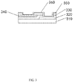
- FIG. 3 is a view schematically illustrating a cross-sectional structure of the array substrate illustrated in FIG. 2 .
- FIG. 3 is a cross-sectional view illustrating the array substrate AA' illustrated in FIG. 2 .
- the second signal line is a signal line 340 of the array substrate and the first signal line is a signal lead-out line 320 of the corresponding signal line.
- the array substrate can include: a substrate 310; a signal lead-out line 320 disposed on the substrate 310; a first insulating layer 330 disposed on the signal lead-out line 320; a signal line 340 disposed on the first insulating layer 330; a second insulating layer 350 disposed on the signal line 340; and a conductive connection layer 360 disposed on the second insulating layer 350.
- the above array substrate can be manufactured by the following process: A first metal layer can be deposited on the substrate 310 by, for example, a sputtering process.
- a pattern of the metal signal lead-out lines 320 can be formed on the first metal layer by a wet etching process.
- the first insulating layer 330 can be deposited on the pattern of the metal signal lead-out lines 320, for example, by a chemical vapor deposition (CVD) process.
- CVD chemical vapor deposition
- a second metal layer can be deposited on the first insulating layer 330 by a sputtering process.
- a pattern of the signal lines 340 can be formed on the second metal layer by a wet etching process.
- a second insulating layer 350 can be deposited on the formed pattern of the signal line 340 by a CVD process.
- via holes in the signal line 340 and the signal lead-out line 320 can be formed by a dry etching process.
- the conductive connection layer 360 is deposited on the second insulating layer 350, and a pattern of the conductive connection layer 360 is formed by etching.
- FIG. 4 is a view schematically illustrating another array substrate according to an exemplary embodiment of the present disclosure.
- an array substrate provided by an embodiment of the present disclosure includes a plurality of first signal lines and a plurality of second signal lines and there is a mapping relationship between the respective first signal lines and the respective second signal lines.
- the first extension portions of the first signal lines are parallel to each other, for example, in the first direction.
- the first connection portions of the first signal lines are parallel to each other, for example, in the second direction.
- the second extension portions of the second signal lines are parallel to each other, for example, in the second direction.
- the second connection portions of the second signal lines are parallel to each other, for example, in the second direction.
- the distance D' between two adjacent second signal lines is reduced, such that a compact design of the wiring of the array substrate can be assured, and connection impedance between the signal line and the corresponding signal lead-out line is reduced.
- the second signal line is a signal line of the array substrate in the above-described embodiment.
- the first signal line is a signal line of the array substrate
- the distance between two adjacent first signal lines is reduced, such that a compact design of the wiring of the array substrate can be assured, and connection impedance between the signal line and the corresponding signal lead-out line is reduced.
- FIG. 5 is a view schematically illustrating another array substrate according to an exemplary embodiment of the present disclosure.
- a shape of a neighboring boundary between the first connection portion and the second connection portion can be a square wave shape.
- the present disclosure is not limited thereto, and the shape of the neighboring boundary between the first connection portion and the second connection portion can be any one or more of a zigzag shape, an arc shape and an irregular shape.
- a length of the neighboring boundary between the first connection portion of the first signal line and the second connection portion of the second signal line is increased by forming the neighboring boundary in the shape as illustrated in FIG. 5 . Therefore, it is possible to further reduce the connection impedance between the signal line and its corresponding signal lead-out line and at the same time remain a reduced distance D' between two adjacent signal lines, such that a compact design of the wiring of the array substrate can be assured, which is beneficial for the design of the narrow frame of the display panel.
- the shape of the neighboring boundary between the first connection portion and the second connection portion can also be any one or more of a zigzag shape, an arc shape and an irregular shape.
- the length of the neighboring boundary between the first connection portion and the second connection portion can be increased as well, therefore, it is possible to further reduce the connection impedance between the signal line and its corresponding signal lead-out line and at the same time remain a reduced distance D' between two adjacent signal lines, such that a compact design of the wiring of the array substrate can be assured, which is beneficial for the design of the narrow frame of the display panel.
- a density of the via holes in the first connection portion and the second connection portion can be correspondingly increased as well.
- FIG. 6 is a view schematically illustrating still another array substrate according to an exemplary embodiment of the present disclosure.
- the second signal line 220 further includes a fourth connection portion 223 in the first direction, which is provided with via holes 240.
- the conductive connection layer 230 is further configured to connect the first signal line 210 and the second signal line 220 through the via holes 240 of the third connection portion 213 and the via holes 240 of the fourth connection portion 223.
- the third connection portion 213 and the fourth connection portion 223 are lined up in a direction perpendicular to the first direction.
- a sum of widths of the third connection portion 213 and the fourth connection portion 223 is not greater than a width of a first extension portion 211.
- width in the embodiments of the present disclosure refers to a width in a direction perpendicular to an extension direction of the first signal line 210.
- an engaging structure is formed between the third connection portion 213 and the fourth connection portion 223.
- the sum of the widths of the third connection portion 213 and the fourth connection portion 223 is approximately equal to the width of the first extension portion 211, and the engaging structure is formed between the third connection portion 213 and the fourth connection portion 223.
- the impedance of the lapping region can be reduced to realize the purpose of reducing the impedance; on the other hand, the space D' between two adjacent second signal lines can be further decreased, such that the wiring of the second signal lines can be more compact, which is beneficial for the implementation of the narrow frame of the display panel.
- the sum of the widths of the third connection portion 213 and the fourth connection portion 223 may be smaller than the width of the first extension portion 211 in other embodiments; or the sum of the widths of the third connection portion 213 and the fourth connection portion 223 may be greater than the width of the first extension portion 211, which is not limited by the present disclosure.
- the third connection portion 213 is disposed on a first side (e.g. a right side in the figure) of the fourth connection portion 223. In other embodiments, the third connection portion 213 may also be disposed on a second side of the fourth connection portion 223 (e.g. on a left side of the fourth connection portion 223), which is not limited by the present disclosure.
- a length of a boundary between the respective connection portions of the first signal line and the second signal line can be further increased by additionally providing the third connection portion of the first signal line and the fourth connection portion of the second signal line. Therefore, it is possible to further reduce the connection impedance between the signal line and its corresponding signal lead-out line and at the same time remain a reduced distance D' between two adjacent signal lines, such that the wiring of the second signal lines can be more compact, which is beneficial for the implementation of the narrow frame of the display panel.
- a shape of the neighboring boundary between the third connection portion and the fourth connection portion in FIG. 6 can be any one or more of a rectangular pulse shape, a zigzag shape, an arc shape and an irregular shape as well.
- the length of the neighboring boundary between the third connection portion and the fourth connection portion can be increased as well, therefore, it is possible to further reduce the connection impedance between the signal line and its corresponding signal lead-out line and at the same time remain a reduced distance D' between two adjacent signal lines, such that the wiring of the second signal lines can be more compact, which is beneficial for the implementation of the narrow frame of the display panel.
- the exemplary embodiment further discloses a display panel including the array substrate described in any of the above embodiments.
- the display panel has the same technical features and working principles as those of the above array substrate and the above contents have been described in detail, thus details thereof will not be described herein again.
- the exemplary embodiment further discloses a display device including the display panel described in any of the above embodiments.
Landscapes
- Physics & Mathematics (AREA)
- Nonlinear Science (AREA)
- Devices For Indicating Variable Information By Combining Individual Elements (AREA)
- Engineering & Computer Science (AREA)
- Microelectronics & Electronic Packaging (AREA)
- Mathematical Physics (AREA)
- Chemical & Material Sciences (AREA)
- Crystallography & Structural Chemistry (AREA)
- General Physics & Mathematics (AREA)
- Optics & Photonics (AREA)
Abstract
Description
- The present disclosure claims priority to Chinese Application No.
201820712571.1, filed May 14, 2018 - The present disclosure relates to display technologies, and more particularly, to an array substrate, a display panel and a display device.
- With the industrial progress and improvement of processes of thin film transistors, liquid crystal display devices have been applied to more and more panel display products such as mobile phones, digital cameras, tablet computers, notebook computers and LCD TVs, and their excellent display characteristics have been highly praised by more and more users and their market competitiveness is strong.
- A Thin Film Transistor Liquid Crystal Display (TFT LCD) is a display device with a wide size range, low energy consumption and low radiation. A thin film transistor liquid crystal display panel is generally composed of an array substrate (a substrate on which thin film transistors (TFT) are formed), a Color Filter (CF) and a liquid crystal layer filled in a cell gap formed by aligning the above two.
- In an array substrate, there are usually a variety of signal lines. The signal lines are usually connected to a binding region through corresponding signal lead-out lines in a peripheral region of the substrate.
- The foregoing information disclosed in Background are only for better understanding of the background of the present disclosure and therefore it can include information that does not constitute the relevant technology already known to those of ordinary skill in the art.
- Other features and advantages of the present disclosure will be apparent from the following detailed descriptions, and may be partially learned by practice of the present disclosure.
- According to a first aspect of the present disclosure, there is provided an array substrate, including: a first signal line including a first extension portion in a first direction and a first connection portion in a second direction, wherein the first connection portion is provided with via holes; a second signal line including a second extension portion and a second connection portion in the second direction, wherein the second connection portion is provided with via holes; and a conductive connection layer configured to connect the first signal line and the second signal line through the via holes of the first connection portion and the via holes of the second connection portion; wherein the first connection portion and the second connection portion are lined up in a direction perpendicular to the second direction.
- According to an embodiment of the present disclosure, a sum of widths of the first connection portion and the second connection portion is not greater than a width of the second extension portion.
- According to an embodiment of the present disclosure, an engaging structure is formed between the first connection portion and the second connection portion.
- According to an embodiment of the present disclosure, a shape of a neighboring boundary between the first connection portion and the second connection portion is any one or more of a square wave shape, a zigzag shape, an arc shape and an irregular shape.
- According to an embodiment of the present disclosure, the first signal line further includes a third connection portion in the first direction, and the third connection portion is provided with via holes; the second signal line further includes a fourth connection portion in the first direction, and the fourth connection portion is provided with via holes; the conductive connection layer is further configured to connect the first signal line and the second signal line through the via holes of the third connection portion and the via holes of the fourth connection portion; and the third connection portion and the fourth connection portion are lined up in a direction perpendicular to the first direction.
- According to an embodiment of the present disclosure, a sum of widths of the third connection portion and the fourth connection portion is not greater than a width of the first extension portion.
- According to an embodiment of the present disclosure, an engaging structure is formed between the third connection portion and the fourth connection portion.
- According to an embodiment of the present disclosure, a shape of a neighboring boundary between the third connection portion and the fourth connection portion is any one or more of a square wave shape, a zigzag shape, an arc shape and an irregular shape.
- According to an embodiment of the present disclosure, the first signal line is a signal line in the array substrate and the second signal line is a signal lead-out line of the corresponding signal line, or the second signal line is a signal line in the array substrate and the first signal line is a signal lead-out line of the corresponding signal line.
- According to an embodiment of the present disclosure, the signal lines includes any one of a gate line, a data line, a common electrode line, a clock signal line and a touch line.
- According to an embodiment of the present disclosure, the first direction is perpendicular to the second direction.
- According to a second aspect of the present disclosure, there is provided a display panel, including the array substrate according to any one of the above embodiments.
- According to a second aspect of the present disclosure, there is provided a display device, including the display panel according to any one of the above embodiments.
- According to a second aspect of the present disclosure, there is provided a method for manufacturing an array substrate, including: depositing a first metal layer on a substrate and forming a first signal line on the first metal layer, wherein the first signal line includes a first extension portion in a first direction and a first connection portion in a second direction; depositing a first insulating layer on the first metal layer, depositing a second metal layer on the first insulating layer and forming a second signal line on the second metal layer, wherein the second signal line includes a second extension portion and a second connection portion in the second direction; depositing a second insulating layer on the second metal layer, forming via holes of the first connection portion by penetrating the second insulating layer and the second metal layer and forming via holes of the second connection portion by penetrating the second insulating layer; and depositing a conductive connection layer on the second insulating layer and forming a pattern on the conductive connection layer etching, wherein the first signal line and the second signal line are connected through the via holes of the first connection portion and the via holes of the second connection portion in the pattern; wherein the first connection portion and the second connection portion are lined up in a direction perpendicular to the second direction.
- According to an embodiment of the present disclosure, a sum of widths of the first connection portion and the second connection portion is not greater than a width of the second extension portion.
- According to an embodiment of the present disclosure, an engaging structure is formed between the first connection portion and the second connection portion.
- According to an embodiment of the present disclosure, a shape of a neighboring boundary between the first connection portion and the second connection portion is any one or more of a square wave shape, a zigzag shape, an arc shape and an irregular shape.
- According to an embodiment of the present disclosure, forming the first signal line further includes forming a third connection portion in the first direction, and third connection portion is provided with via holes; forming the second signal line further includes forming a fourth connection portion in the first direction, and the fourth connection portion is provided with via holes; forming the conductive connection layer further includes forming a pattern on the conductive connection layer by etching, wherein the first signal line and the second signal line are connected through the via holes of the third connection portion and the via holes of the fourth connection portion in the pattern; and the third connection portion and the fourth connection portion are lined up in a direction perpendicular to the first direction.
- According to an embodiment of the present disclosure, a sum of widths of the third connection portion and the fourth connection portion is not greater than a width of the first extension portion.
- According to an embodiment of the present disclosure, an engaging structure is formed between the third connection portion and the fourth connection portion.
- It is to be understood that both the foregoing general description and the following detailed description are exemplary and explanatory only and are not restrictive of the disclosure, as claimed.
- The accompanying drawings, which are incorporated in and constitute a part of this specification, illustrate embodiments consistent with the utility model and, together with the description, serve to explain the principles of the utility model.
-
FIG 1 is a view schematically illustrating an array substrate in the relevant technology. -
FIG 2 is a view schematically illustrating an array substrate according to an exemplary embodiment of the present disclosure. -
FIG 3 is a view schematically illustrating a cross-sectional structure of the array substrate illustrated inFIG 2 . -
FIG 4 is a view schematically illustrating another array substrate according to an exemplary embodiment of the present disclosure. -
FIG 5 is a view schematically illustrating still another array substrate according to an exemplary embodiment of the present disclosure. -
FIG. 6 is a view schematically illustrating still another array substrate according to an exemplary embodiment of the present disclosure. - The exemplary implementations will now be described more fully with reference to the accompanying drawings. Example embodiments can be embodied in many forms, and should not be construed as being limited to the examples set forth herein; rather, the implementations are provided so that the disclosure will be thorough and complete, and will fully convey the conception of exemplary implementations to those skilled in the art. The drawings are only schematic representations of the disclosure, and are not necessarily drawn to scale. The same reference numerals throughout the drawings denote the same or like parts, thus their detailed description will be omitted.
- In addition, the features, structures or characteristics described herein can be included in one or more embodiments in any appropriate way. In the description hereinafter, many specific details are provided for fully understanding of the embodiments of the present disclosure. However, it will be appreciated by those skilled in the art that the technical solution of the present disclosure can be practiced without one or more of the specific details, or with other methods, components, devices or steps. In addition, known structures, methods, devices, implementations, materials or operations will not be illustrated or described in detail, to avoid obscuration of the aspects of the present disclosure.
- Some of the block diagrams shown in the drawings are functional entities and are not necessarily corresponding to physically or logically separate entities. These functional entities may be implemented in software, or implemented in one or more hardware modules or integrated circuits, or implemented in different network and/or processor devices and/or microcontroller devices.
- The implementations set forth in the following description of exemplary embodiments do not represent all implementations consistent with the utility model. Instead, they are merely examples of devices and methods consistent with aspects related to the utility model as recited in the appended claims.
-
FIG. 1 is a view schematically illustrating an array substrate in the relevant technology. - In an array substrate, there are generally many kinds of
signal lines 102 which are usually connected to a binding region through corresponding signal lead-outlines 101 in a peripheral region of the substrate. Thesignal lines 102 and their respective signal lead-outlines 101 are not in direct connections for some design reasons (they are disposed on different layers, or for anti-static purpose, etc.). Rather, thesignal lines 102 and their respective signal lead-outlines 101 are lapped by adding aconductive connection layer 103, and are connected through theirvia holes 104. For example, the connection manner of the signal lines and the signal lead-out lines in the relevant technology is as illustrated inFIG 1 . - To reduce an impedance of a lapping region, a width of the conductive connection layer will be generally increased to realize the purpose of reducing the impedance. However, such design may lead a space D between the adjacent signal lines to be increased, which is disadvantageous for wiring of the peripheral region, and thus disadvantageous for realizing a narrow frame of a display panel.
-
FIG. 2 is a view schematically illustrating an array substrate according to an exemplary embodiment of the present disclosure. - As illustrated in
FIG. 2 , embodiments of the present disclosure provide an array substrate. The array substrate can include afirst signal line 210, asecond signal line 220 and aconductive connection layer 230. - The
first signal line 210 can include afirst extension portion 211 in a first direction (e.g. an X-axis direction in the figure, but the present disclosure is not limited thereto) and afirst connection portion 212 in a second direction (e.g. a Y-axis direction in the figure, but the present disclosure is not limited thereto).In the embodiment, viaholes 240 can be disposed in thefirst connection portion 212. - The
second signal line 220 can include asecond extension portion 221 and asecond connection portion 222 in the second direction. In the embodiment, viaholes 240 can be disposed in thesecond connection portion 222. - The
conductive connection layer 230 can be configured to connect thefirst signal line 210 and thesecond signal line 220 through the via holes 240 of thefirst connection portion 212 and the via holes 240 of thesecond connection portion 222. - The
first connection portion 212 and thesecond connection portion 222 are lined up in a direction substantially perpendicular to the second direction. - In the embodiment illustrated in
FIG. 2 , the first direction can be perpendicular to the second direction. At this time, thefirst connection portion 212 of thefirst signal line 210 and thesecond connection portion 222 of thesecond signal line 220 are lined up in the first direction. A number of viaholes 240 are respectively disposed on thefirst connection portion 212 and thesecond connection portion 222. - In an exemplary embodiment, a sum of a width W11 of the
first connection portion 212 and a width W12 of thesecond connection portion 222 is not greater than a width W1 of thesecond extension portion 221. - It should be noted that "width" in the embodiments of the present disclosure refers to a width in a direction perpendicular to an extension direction of the
second signal line 220. - In an exemplary embodiment, an engaging structure is formed between the
first connection portion 212 and thesecond connection portion 222. - In the embodiment illustrated in
FIG. 2 , the sum of the widths of thefirst connection portion 212 and thesecond connection portion 222 is approximately equal to the width of thesecond extension portion 221, and the engaging structure is formed between thefirst connection portion 212 and thesecond connection portion 222. Therefore, on one hand, the impedance of the lapping region can be reduced to realize the purpose of reducing the impedance; on the other hand, the space D' between two adjacent second signal lines can be further decreased, such that the wiring of the second signal lines can be more compact, which is beneficial for the implementation of the narrow frame of the display panel. - It is to be understood that the sum of the widths of the
first connection portion 212 and thesecond connection portion 222 may be smaller than the width of thesecond extension portion 221 in other embodiments; or the sum of the widths of thefirst connection portion 212 and thesecond connection portion 222 may be greater than the width of thesecond extension portion 221, which is not limited in the present disclosure. - In the embodiment illustrated in
FIG. 2 , thefirst connection portion 212 is disposed on a first side (e.g. above in the figure) of thesecond connection portion 222. In other embodiments, thefirst connection portion 212 may be disposed on a second side of the second connection portion 222 (e.g. below the second connection portion 222) as well, which is not limited in the present disclosure. - In the embodiment illustrated in
FIG. 2 , thesecond signal line 220 can be any kind of signal line in the array substrate, and thefirst signal line 210 can be a signal lead-out line corresponding to that kind of signal line. - In an exemplary embodiment, the signal lines can include any one of a gate line, a data line, a common electrode line, or a clock signal line in the array substrate.
- In an exemplary embodiment, if the array substrate is an array substrate that is integrated with in-plane touch control, the signal lines can further include a touch line.
- In other embodiments, the first signal line can be any kind of signal line in the array substrate and the second signal line can be a signal lead-out line corresponding to that kind of signal line as well.
- In the array substrate provided by the embodiment of the present disclosure, through the first extension portion in the first direction and the first connection portion in the second direction of the first signal line, the second extension portion and the second connection portion in the second direction of the second signal line, and by lining up the first connection portion and the second connection portion in the direction perpendicular to the second direction, it is possible to reduce the space between the adjacent signal lines of the array substrate when the signal lines and their corresponding signal lead-out lines are connected using the conductive connection layers, such that the wiring of the signal lines of the array substrate can be more compact, which is beneficial for the implementation of the narrow frame of the display panel.
-
FIG. 3 is a view schematically illustrating a cross-sectional structure of the array substrate illustrated inFIG. 2 . -
FIG. 3 is a cross-sectional view illustrating the array substrate AA' illustrated inFIG. 2 . Here, explanations will be made by taking an example in which the second signal line is asignal line 340 of the array substrate and the first signal line is a signal lead-outline 320 of the corresponding signal line. - In an embodiment of the present disclosure, the array substrate can include: a
substrate 310; a signal lead-outline 320 disposed on thesubstrate 310; a first insulatinglayer 330 disposed on the signal lead-outline 320; asignal line 340 disposed on the first insulatinglayer 330; a second insulatinglayer 350 disposed on thesignal line 340; and aconductive connection layer 360 disposed on the second insulatinglayer 350. - The above array substrate can be manufactured by the following process:
A first metal layer can be deposited on thesubstrate 310 by, for example, a sputtering process. - For another example, a pattern of the metal signal lead-out
lines 320 can be formed on the first metal layer by a wet etching process. - The first insulating
layer 330 can be deposited on the pattern of the metal signal lead-outlines 320, for example, by a chemical vapor deposition (CVD) process. - For another example, a second metal layer can be deposited on the first insulating
layer 330 by a sputtering process. - For another example, a pattern of the
signal lines 340 can be formed on the second metal layer by a wet etching process. - For another example, a second insulating
layer 350 can be deposited on the formed pattern of thesignal line 340 by a CVD process. - For another example, via holes in the
signal line 340 and the signal lead-outline 320 can be formed by a dry etching process. - The
conductive connection layer 360 is deposited on the second insulatinglayer 350, and a pattern of theconductive connection layer 360 is formed by etching. - It should be noted that the manufacturing process of the array substrate described above is for illustrative purpose only and the present disclosure is not limited thereto.
-
FIG. 4 is a view schematically illustrating another array substrate according to an exemplary embodiment of the present disclosure. - As illustrated in
FIG. 4 , an array substrate provided by an embodiment of the present disclosure includes a plurality of first signal lines and a plurality of second signal lines and there is a mapping relationship between the respective first signal lines and the respective second signal lines. - The first extension portions of the first signal lines are parallel to each other, for example, in the first direction. The first connection portions of the first signal lines are parallel to each other, for example, in the second direction.
- The second extension portions of the second signal lines are parallel to each other, for example, in the second direction. The second connection portions of the second signal lines are parallel to each other, for example, in the second direction.
- As can be seen from
FIG. 4 , the distance D' between two adjacent second signal lines is reduced, such that a compact design of the wiring of the array substrate can be assured, and connection impedance between the signal line and the corresponding signal lead-out line is reduced. - It is shall be understand, explanations are made by taking an example in which the second signal line is a signal line of the array substrate in the above-described embodiment. In other embodiments, when the first signal line is a signal line of the array substrate, similarly, if the above-mentioned array substrate is used, the distance between two adjacent first signal lines is reduced, such that a compact design of the wiring of the array substrate can be assured, and connection impedance between the signal line and the corresponding signal lead-out line is reduced.
-
FIG. 5 is a view schematically illustrating another array substrate according to an exemplary embodiment of the present disclosure. - As illustrated in
FIG. 5 , different from the embodiment illustrated inFIG. 2 , a shape of a neighboring boundary between the first connection portion and the second connection portion can be a square wave shape. However, the present disclosure is not limited thereto, and the shape of the neighboring boundary between the first connection portion and the second connection portion can be any one or more of a zigzag shape, an arc shape and an irregular shape. - In the array substrate provided by the embodiment, a length of the neighboring boundary between the first connection portion of the first signal line and the second connection portion of the second signal line is increased by forming the neighboring boundary in the shape as illustrated in
FIG. 5 . Therefore, it is possible to further reduce the connection impedance between the signal line and its corresponding signal lead-out line and at the same time remain a reduced distance D' between two adjacent signal lines, such that a compact design of the wiring of the array substrate can be assured, which is beneficial for the design of the narrow frame of the display panel. - In other embodiments, the shape of the neighboring boundary between the first connection portion and the second connection portion can also be any one or more of a zigzag shape, an arc shape and an irregular shape. Similarly, the length of the neighboring boundary between the first connection portion and the second connection portion can be increased as well, therefore, it is possible to further reduce the connection impedance between the signal line and its corresponding signal lead-out line and at the same time remain a reduced distance D' between two adjacent signal lines, such that a compact design of the wiring of the array substrate can be assured, which is beneficial for the design of the narrow frame of the display panel.
- In the embodiment illustrated in
FIG. 5 , beside increasing the length of the neighboring boundary between the first connection portion and the second connection portion, at the same time, a density of the via holes in the first connection portion and the second connection portion can be correspondingly increased as well. -
FIG. 6 is a view schematically illustrating still another array substrate according to an exemplary embodiment of the present disclosure. - As illustrated in
FIG. 6 , the difference between the array substrate provided in this embodiment and that in the embodiment illustrated inFIG 2 lies in that thefirst signal line 210 can further include athird connection portion 213 in the first direction, which is provided with viaholes 240. - The
second signal line 220 further includes afourth connection portion 223 in the first direction, which is provided with viaholes 240. - The
conductive connection layer 230 is further configured to connect thefirst signal line 210 and thesecond signal line 220 through the via holes 240 of thethird connection portion 213 and the via holes 240 of thefourth connection portion 223. - The
third connection portion 213 and thefourth connection portion 223 are lined up in a direction perpendicular to the first direction. - In an exemplary embodiment, a sum of widths of the
third connection portion 213 and thefourth connection portion 223 is not greater than a width of afirst extension portion 211. - It should be noted that "width" in the embodiments of the present disclosure refers to a width in a direction perpendicular to an extension direction of the
first signal line 210. - In an exemplary embodiment, an engaging structure is formed between the
third connection portion 213 and thefourth connection portion 223. - In the embodiment illustrated in
FIG 6 , the sum of the widths of thethird connection portion 213 and thefourth connection portion 223 is approximately equal to the width of thefirst extension portion 211, and the engaging structure is formed between thethird connection portion 213 and the fourth connection portion 223.Therefore, on one hand, the impedance of the lapping region can be reduced to realize the purpose of reducing the impedance; on the other hand, the space D' between two adjacent second signal lines can be further decreased, such that the wiring of the second signal lines can be more compact, which is beneficial for the implementation of the narrow frame of the display panel. - It is to be understood that the sum of the widths of the
third connection portion 213 and thefourth connection portion 223 may be smaller than the width of thefirst extension portion 211 in other embodiments; or the sum of the widths of thethird connection portion 213 and thefourth connection portion 223 may be greater than the width of thefirst extension portion 211, which is not limited by the present disclosure. - In the embodiment illustrated in
FIG. 6 , thethird connection portion 213 is disposed on a first side (e.g. a right side in the figure) of thefourth connection portion 223. In other embodiments, thethird connection portion 213 may also be disposed on a second side of the fourth connection portion 223 (e.g. on a left side of the fourth connection portion 223), which is not limited by the present disclosure. - In the array substrate provided by the embodiment of the present disclosure, a length of a boundary between the respective connection portions of the first signal line and the second signal line can be further increased by additionally providing the third connection portion of the first signal line and the fourth connection portion of the second signal line. Therefore, it is possible to further reduce the connection impedance between the signal line and its corresponding signal lead-out line and at the same time remain a reduced distance D' between two adjacent signal lines, such that the wiring of the second signal lines can be more compact, which is beneficial for the implementation of the narrow frame of the display panel.
- In other embodiments, similar to the embodiment illustrated in
FIG. 5 , a shape of the neighboring boundary between the third connection portion and the fourth connection portion inFIG. 6 can be any one or more of a rectangular pulse shape, a zigzag shape, an arc shape and an irregular shape as well. Similarly, the length of the neighboring boundary between the third connection portion and the fourth connection portion can be increased as well, therefore, it is possible to further reduce the connection impedance between the signal line and its corresponding signal lead-out line and at the same time remain a reduced distance D' between two adjacent signal lines, such that the wiring of the second signal lines can be more compact, which is beneficial for the implementation of the narrow frame of the display panel. - The exemplary embodiment further discloses a display panel including the array substrate described in any of the above embodiments.
- The display panel has the same technical features and working principles as those of the above array substrate and the above contents have been described in detail, thus details thereof will not be described herein again.
- The exemplary embodiment further discloses a display device including the display panel described in any of the above embodiments.
- Other embodiments of the present utility model will be apparent to those skilled in the art from consideration of the specification and practice of the utility model disclosed here. This application is intended to cover any variations, uses, or adaptations of the present utility model following the general principles thereof and including such departures from the present disclosure as come within known or customary practice in the art. It is intended that the specification and examples be considered as exemplary only, with a true scope and spirit of the present utility model being indicated by the following claims.
- The exemplary embodiments of the disclosure have been specifically illustrated and described above. It should be understood that the disclosure is not limited to the detailed structures, arrangements or implementations described herein; rather, the disclosure is intended to cover various modifications and equivalents that fall within the spirit and scope of the appended claims.
Claims (20)
- An array substrate, comprising:a first signal line comprising a first extension portion in a first direction and a first connection portion in a second direction, wherein the first connection portion is provided with via holes;a second signal line comprising a second extension portion and a second connection portion in the second direction, wherein the second connection portion is provided with via holes; anda conductive connection layer configured to connect the first signal line and the second signal line through the via holes of the first connection portion and the via holes of the second connection portion;wherein the first connection portion and the second connection portion are lined up in a direction perpendicular to the second direction.
- The array substrate according to claim 1, wherein a sum of widths of the first connection portion and the second connection portion is not greater than a width of the second extension portion.
- The array substrate according to claim 1, wherein an engaging structure is formed between the first connection portion and the second connection portion.
- The array substrate according to claim 3, wherein a shape of a neighboring boundary between the first connection portion and the second connection portion is any one or more of a square wave shape, a zigzag shape, an arc shape and an irregular shape.
- The array substrate according to any one of claims 1-4, wherein the first signal line further comprises a third connection portion in the first direction, and the third connection portion is provided with via holes;
the second signal line further comprises a fourth connection portion in the first direction, and the fourth connection portion is provided with via holes;
the conductive connection layer is further configured to connect the first signal line and the second signal line through the via holes of the third connection portion and the via holes of the fourth connection portion; and
the third connection portion and the fourth connection portion are lined up in a direction perpendicular to the first direction. - The array substrate according to claim 5, wherein a sum of widths of the third connection portion and the fourth connection portion is not greater than a width of the first extension portion.
- The array substrate according to claim 5, wherein an engaging structure is formed between the third connection portion and the fourth connection portion.
- The array substrate according to claim 7, wherein a shape of a neighboring boundary between the third connection portion and the fourth connection portion is any one or more of a square wave shape, a zigzag shape, an arc shape and an irregular shape.
- The array substrate according to claim 1, wherein the first signal line is a signal line in the array substrate and the second signal line is a signal lead-out line of the corresponding signal line, or the second signal line is a signal line in the array substrate and the first signal line is a signal lead-out line of the corresponding signal line.
- The array substrate according to claim 9, wherein the signal lines comprise any one of a gate line, a data line, a common electrode line, a clock signal line and a touch line.
- The array substrate according to claim 1, wherein the first direction is perpendicular to the second direction.
- A display panel, comprising the array substrate according to any one of claims 1-11.
- A display device, comprising the display panel according to claim 12.
- A method for manufacturing an array substrate, comprising:depositing a first metal layer on a substrate and forming a first signal line on the first metal layer, wherein the first signal line comprises a first extension portion in a first direction and a first connection portion in a second direction;depositing a first insulating layer on the first metal layer, depositing a second metal layer on the first insulating layer and forming a second signal line on the second metal layer, wherein the second signal line comprises a second extension portion and a second connection portion in the second direction;depositing a second insulating layer on the second metal layer, forming via holes of the first connection portion by penetrating the second insulating layer and the second metal layer and forming via holes of the second connection portion by penetrating the second insulating layer; anddepositing a conductive connection layer on the second insulating layer and forming a pattern on the conductive connection layer etching, wherein the first signal line and the second signal line are connected through the via holes of the first connection portion and the via holes of the second connection portion in the pattern;wherein the first connection portion and the second connection portion are lined up in a direction perpendicular to the second direction.
- The array substrate according to claim 14, wherein a sum of widths of the first connection portion and the second connection portion is not greater than a width of the second extension portion.
- The array substrate according to claim 14, wherein an engaging structure is formed between the first connection portion and the second connection portion.
- The array substrate according to claim 16, wherein a shape of a neighboring boundary between the first connection portion and the second connection portion is any one or more of a square wave shape, a zigzag shape, an arc shape and an irregular shape.
- The array substrate according to any one of claims 14-17, wherein forming the first signal line further comprises forming a third connection portion in the first direction, and third connection portion is provided with via holes;
forming the second signal line further comprises forming a fourth connection portion in the first direction, and the fourth connection portion is provided with via holes;
forming the conductive connection layer further comprises forming a pattern on the conductive connection layer by etching, wherein the first signal line and the second signal line are connected through the via holes of the third connection portion and the via holes of the fourth connection portion in the pattern; and
the third connection portion and the fourth connection portion are lined up in a direction perpendicular to the first direction. - The array substrate according to claim 18, wherein a sum of widths of the third connection portion and the fourth connection portion is not greater than a width of the first extension portion.
- The array substrate according to claim 18, wherein an engaging structure is formed between the third connection portion and the fourth connection portion.
Applications Claiming Priority (2)
| Application Number | Priority Date | Filing Date | Title |
|---|---|---|---|
| CN201820712571.1U CN208488633U (en) | 2018-05-14 | 2018-05-14 | Array substrate, display panel and display device |
| PCT/CN2019/081588 WO2019218799A1 (en) | 2018-05-14 | 2019-04-04 | Array substrate, display panel, and display device |
Publications (3)
| Publication Number | Publication Date |
|---|---|
| EP3796077A1 true EP3796077A1 (en) | 2021-03-24 |
| EP3796077A4 EP3796077A4 (en) | 2022-05-04 |
| EP3796077B1 EP3796077B1 (en) | 2025-12-31 |
Family
ID=65253149
Family Applications (1)
| Application Number | Title | Priority Date | Filing Date |
|---|---|---|---|
| EP19804564.3A Active EP3796077B1 (en) | 2018-05-14 | 2019-04-04 | Display substrate, display board and display device |
Country Status (5)
| Country | Link |
|---|---|
| US (1) | US11276713B2 (en) |
| EP (1) | EP3796077B1 (en) |
| JP (1) | JP7343396B2 (en) |
| CN (1) | CN208488633U (en) |
| WO (1) | WO2019218799A1 (en) |
Families Citing this family (2)
| Publication number | Priority date | Publication date | Assignee | Title |
|---|---|---|---|---|
| CN208488633U (en) | 2018-05-14 | 2019-02-12 | 北京京东方技术开发有限公司 | Array substrate, display panel and display device |
| CN111999947A (en) * | 2020-08-11 | 2020-11-27 | 深圳市华星光电半导体显示技术有限公司 | Display panel and display device |
Family Cites Families (22)
| Publication number | Priority date | Publication date | Assignee | Title |
|---|---|---|---|---|
| JP3050738B2 (en) | 1993-12-17 | 2000-06-12 | シャープ株式会社 | Display device drive circuit |
| TWI363206B (en) | 2003-02-28 | 2012-05-01 | Samsung Electronics Co Ltd | Liquid crystal display device |
| US7714820B2 (en) * | 2003-06-27 | 2010-05-11 | Samsung Electronics Co., Ltd. | Contact structure of conductive films and thin film transistor array panel including the same |
| KR20080008703A (en) | 2006-07-21 | 2008-01-24 | 삼성전자주식회사 | Array substrate, display panel having same and manufacturing method thereof |
| JP4305486B2 (en) * | 2006-09-28 | 2009-07-29 | エプソンイメージングデバイス株式会社 | LCD panel |
| KR20080036747A (en) * | 2006-10-24 | 2008-04-29 | 삼성전자주식회사 | Display device and manufacturing method thereof |
| JP4356750B2 (en) * | 2007-01-25 | 2009-11-04 | エプソンイメージングデバイス株式会社 | Liquid crystal display device and manufacturing method thereof |
| JP5420760B2 (en) * | 2010-04-22 | 2014-02-19 | シャープ株式会社 | Active matrix substrate and display device |
| KR101759985B1 (en) * | 2010-10-20 | 2017-07-21 | 삼성디스플레이 주식회사 | Gate driver and Liquid crystal display comprising thereof |
| KR101307260B1 (en) * | 2012-03-29 | 2013-09-10 | 엘지디스플레이 주식회사 | Line on glass type liquid crystal display device and method of fabricating the same |
| CN202693965U (en) * | 2012-07-25 | 2013-01-23 | 北京京东方光电科技有限公司 | Array substrate and display device |
| CN204422935U (en) | 2015-03-12 | 2015-06-24 | 京东方科技集团股份有限公司 | A kind of array base palte and display device |
| JP2016224296A (en) * | 2015-06-01 | 2016-12-28 | 株式会社ジャパンディスプレイ | Display device |
| CN105607361A (en) * | 2015-12-30 | 2016-05-25 | 上海中航光电子有限公司 | Array substrate, display panel and display device |
| CN107135359B (en) * | 2016-02-26 | 2020-04-14 | 上海箩箕技术有限公司 | Image acquisition method of TFT flat-panel image sensor |
| KR102585124B1 (en) * | 2016-04-20 | 2023-10-05 | 삼성디스플레이 주식회사 | Display device and manufacturing method thereof |
| CN106169482B (en) * | 2016-08-01 | 2019-04-09 | 京东方科技集团股份有限公司 | A substrate and its manufacturing method, electronic device |
| CN106125437B (en) * | 2016-09-05 | 2019-07-16 | 京东方科技集团股份有限公司 | Display base plate and preparation method thereof, display device |
| CN107479283B (en) | 2017-08-30 | 2020-07-07 | 厦门天马微电子有限公司 | Array substrate, display panel and display device |
| CN107945726A (en) * | 2017-11-22 | 2018-04-20 | 深圳市华星光电技术有限公司 | A kind of array base palte and display panel |
| CN208488633U (en) * | 2018-05-14 | 2019-02-12 | 北京京东方技术开发有限公司 | Array substrate, display panel and display device |
| CN108878444B (en) * | 2018-06-07 | 2021-11-19 | 武汉天马微电子有限公司 | Display panel and display device |
-
2018
- 2018-05-14 CN CN201820712571.1U patent/CN208488633U/en active Active
-
2019
- 2019-04-04 US US16/630,738 patent/US11276713B2/en active Active
- 2019-04-04 EP EP19804564.3A patent/EP3796077B1/en active Active
- 2019-04-04 WO PCT/CN2019/081588 patent/WO2019218799A1/en not_active Ceased
- 2019-04-04 JP JP2019559832A patent/JP7343396B2/en active Active
Also Published As
| Publication number | Publication date |
|---|---|
| EP3796077B1 (en) | 2025-12-31 |
| US20210013233A1 (en) | 2021-01-14 |
| CN208488633U (en) | 2019-02-12 |
| EP3796077A4 (en) | 2022-05-04 |
| US11276713B2 (en) | 2022-03-15 |
| JP2021521470A (en) | 2021-08-26 |
| JP7343396B2 (en) | 2023-09-12 |
| WO2019218799A1 (en) | 2019-11-21 |
Similar Documents
| Publication | Publication Date | Title |
|---|---|---|
| EP2743766B1 (en) | Manufacturing method for array substrate | |
| US12201001B2 (en) | Array substrate and display device | |
| US10282004B2 (en) | Substrate, method for manufacturing the same, and display device | |
| US10790310B2 (en) | Array substrate, display panel and display device with metal connecting member to reduce contact resistance | |
| US9612495B2 (en) | Array substrate and display device | |
| CN105824161B (en) | A liquid crystal display panel and a liquid crystal display device | |
| CN103456744B (en) | Array base palte and preparation method thereof, display device | |
| CN104950540B (en) | Array substrate and preparation method thereof and display device | |
| CN205645811U (en) | Array baseplate and display device | |
| US11573666B2 (en) | Display device with touch control wiring liens having hole patterns and method of manufacturing thereof | |
| CN105404062A (en) | Array substrate and display device | |
| CN104701302A (en) | Array substrate and manufacture method thereof and display device | |
| WO2020034296A1 (en) | Electrostatic discharge unit, array substrate and liquid crystal display panel | |
| WO2016141705A1 (en) | Array substrate and manufacturing method thereof, and display device | |
| US11276713B2 (en) | Array substrate, manufacturing method, display panel and display device thereof | |
| JP2020507208A (en) | Array substrate and method of manufacturing array substrate | |
| CN104538413A (en) | Array substrate, manufacturing method thereof and display device | |
| EP4235286B1 (en) | Pixel structure, array substrate and display device | |
| CN115390302A (en) | Liquid crystal display panel and preparation method thereof | |
| US10678105B2 (en) | Array substrate and manufacturing method thereof and liquid crystal display apparatus | |
| CN205620654U (en) | Liquid crystal display panel and liquid crystal display device | |
| CN115548080A (en) | Display panel and display device | |
| CN112596315A (en) | Array substrate, preparation method thereof and display device | |
| TWI835653B (en) | Display panel | |
| US20210141494A1 (en) | Touch screen, manufacturing method thereof, and display device |
Legal Events
| Date | Code | Title | Description |
|---|---|---|---|
| STAA | Information on the status of an ep patent application or granted ep patent |
Free format text: STATUS: THE INTERNATIONAL PUBLICATION HAS BEEN MADE |
|
| PUAI | Public reference made under article 153(3) epc to a published international application that has entered the european phase |
Free format text: ORIGINAL CODE: 0009012 |
|
| STAA | Information on the status of an ep patent application or granted ep patent |
Free format text: STATUS: REQUEST FOR EXAMINATION WAS MADE |
|
| 17P | Request for examination filed |
Effective date: 20200124 |
|
| AK | Designated contracting states |
Kind code of ref document: A1 Designated state(s): AL AT BE BG CH CY CZ DE DK EE ES FI FR GB GR HR HU IE IS IT LI LT LU LV MC MK MT NL NO PL PT RO RS SE SI SK SM TR |
|
| AX | Request for extension of the european patent |
Extension state: BA ME |
|
| DAV | Request for validation of the european patent (deleted) | ||
| DAX | Request for extension of the european patent (deleted) | ||
| REG | Reference to a national code |
Ref country code: DE Free format text: PREVIOUS MAIN CLASS: G02F0001136200 Ref country code: DE Ref legal event code: R079 Ref document number: 602019079866 Country of ref document: DE Free format text: PREVIOUS MAIN CLASS: G02F0001136200 Ipc: H01L0027120000 |
|
| A4 | Supplementary search report drawn up and despatched |
Effective date: 20220407 |
|
| RIC1 | Information provided on ipc code assigned before grant |
Ipc: G02F 1/1362 20060101ALI20220401BHEP Ipc: H01L 27/12 20060101AFI20220401BHEP |
|
| STAA | Information on the status of an ep patent application or granted ep patent |
Free format text: STATUS: EXAMINATION IS IN PROGRESS |
|
| 17Q | First examination report despatched |
Effective date: 20240605 |
|
| REG | Reference to a national code |
Ref country code: DE Ref legal event code: R079 Free format text: PREVIOUS MAIN CLASS: H01L0027120000 Ref country code: DE Ref legal event code: R079 Ref document number: 602019079866 Country of ref document: DE Free format text: PREVIOUS MAIN CLASS: H01L0027120000 Ipc: H10D0086400000 |
|
| GRAP | Despatch of communication of intention to grant a patent |
Free format text: ORIGINAL CODE: EPIDOSNIGR1 |
|
| STAA | Information on the status of an ep patent application or granted ep patent |
Free format text: STATUS: GRANT OF PATENT IS INTENDED |
|
| RIC1 | Information provided on ipc code assigned before grant |
Ipc: H10D 86/40 20250101AFI20250801BHEP Ipc: G02F 1/1362 20060101ALI20250801BHEP Ipc: H10D 86/60 20250101ALI20250801BHEP |
|
| INTG | Intention to grant announced |
Effective date: 20250901 |
|
| GRAS | Grant fee paid |
Free format text: ORIGINAL CODE: EPIDOSNIGR3 |
|
| GRAA | (expected) grant |
Free format text: ORIGINAL CODE: 0009210 |
|
| STAA | Information on the status of an ep patent application or granted ep patent |
Free format text: STATUS: THE PATENT HAS BEEN GRANTED |
|
| AK | Designated contracting states |
Kind code of ref document: B1 Designated state(s): AL AT BE BG CH CY CZ DE DK EE ES FI FR GB GR HR HU IE IS IT LI LT LU LV MC MK MT NL NO PL PT RO RS SE SI SK SM TR |
|
| REG | Reference to a national code |
Ref country code: CH Ref legal event code: F10 Free format text: ST27 STATUS EVENT CODE: U-0-0-F10-F00 (AS PROVIDED BY THE NATIONAL OFFICE) Effective date: 20251231 Ref country code: GB Ref legal event code: FG4D |
|
| REG | Reference to a national code |
Ref country code: DE Ref legal event code: R096 Ref document number: 602019079866 Country of ref document: DE |
|
| REG | Reference to a national code |
Ref country code: IE Ref legal event code: FG4D |
|
| PGFP | Annual fee paid to national office [announced via postgrant information from national office to epo] |
Ref country code: GB Payment date: 20260323 Year of fee payment: 8 |
|
| REG | Reference to a national code |
Ref country code: LT Ref legal event code: MG9D |
|
| PG25 | Lapsed in a contracting state [announced via postgrant information from national office to epo] |
Ref country code: NO Free format text: LAPSE BECAUSE OF FAILURE TO SUBMIT A TRANSLATION OF THE DESCRIPTION OR TO PAY THE FEE WITHIN THE PRESCRIBED TIME-LIMIT Effective date: 20260331 |
|
| PG25 | Lapsed in a contracting state [announced via postgrant information from national office to epo] |
Ref country code: HR Free format text: LAPSE BECAUSE OF FAILURE TO SUBMIT A TRANSLATION OF THE DESCRIPTION OR TO PAY THE FEE WITHIN THE PRESCRIBED TIME-LIMIT Effective date: 20251231 Ref country code: FI Free format text: LAPSE BECAUSE OF FAILURE TO SUBMIT A TRANSLATION OF THE DESCRIPTION OR TO PAY THE FEE WITHIN THE PRESCRIBED TIME-LIMIT Effective date: 20251231 |
|
| PG25 | Lapsed in a contracting state [announced via postgrant information from national office to epo] |
Ref country code: RS Free format text: LAPSE BECAUSE OF FAILURE TO SUBMIT A TRANSLATION OF THE DESCRIPTION OR TO PAY THE FEE WITHIN THE PRESCRIBED TIME-LIMIT Effective date: 20260331 |
|
| PG25 | Lapsed in a contracting state [announced via postgrant information from national office to epo] |
Ref country code: LV Free format text: LAPSE BECAUSE OF FAILURE TO SUBMIT A TRANSLATION OF THE DESCRIPTION OR TO PAY THE FEE WITHIN THE PRESCRIBED TIME-LIMIT Effective date: 20251231 |