EP3794646B1 - Sensor and method for discriminating between wavelength regions using the sensor - Google Patents
Sensor and method for discriminating between wavelength regions using the sensor Download PDFInfo
- Publication number
- EP3794646B1 EP3794646B1 EP19827313.8A EP19827313A EP3794646B1 EP 3794646 B1 EP3794646 B1 EP 3794646B1 EP 19827313 A EP19827313 A EP 19827313A EP 3794646 B1 EP3794646 B1 EP 3794646B1
- Authority
- EP
- European Patent Office
- Prior art keywords
- substrate
- sensor according
- sensing element
- flake
- black phosphorus
- Prior art date
- Legal status (The legal status is an assumption and is not a legal conclusion. Google has not performed a legal analysis and makes no representation as to the accuracy of the status listed.)
- Active
Links
Images






Classifications
-
- G—PHYSICS
- G01—MEASURING; TESTING
- G01J—MEASUREMENT OF INTENSITY, VELOCITY, SPECTRAL CONTENT, POLARISATION, PHASE OR PULSE CHARACTERISTICS OF INFRARED, VISIBLE OR ULTRAVIOLET LIGHT; COLORIMETRY; RADIATION PYROMETRY
- G01J1/00—Photometry, e.g. photographic exposure meter
- G01J1/42—Photometry, e.g. photographic exposure meter using electric radiation detectors
- G01J1/429—Photometry, e.g. photographic exposure meter using electric radiation detectors applied to measurement of ultraviolet light
-
- H—ELECTRICITY
- H10—SEMICONDUCTOR DEVICES; ELECTRIC SOLID-STATE DEVICES NOT OTHERWISE PROVIDED FOR
- H10F—INORGANIC SEMICONDUCTOR DEVICES SENSITIVE TO INFRARED RADIATION, LIGHT, ELECTROMAGNETIC RADIATION OF SHORTER WAVELENGTH OR CORPUSCULAR RADIATION
- H10F30/00—Individual radiation-sensitive semiconductor devices in which radiation controls the flow of current through the devices, e.g. photodetectors
- H10F30/20—Individual radiation-sensitive semiconductor devices in which radiation controls the flow of current through the devices, e.g. photodetectors the devices having potential barriers, e.g. phototransistors
- H10F30/21—Individual radiation-sensitive semiconductor devices in which radiation controls the flow of current through the devices, e.g. photodetectors the devices having potential barriers, e.g. phototransistors the devices being sensitive to infrared, visible or ultraviolet radiation
- H10F30/28—Individual radiation-sensitive semiconductor devices in which radiation controls the flow of current through the devices, e.g. photodetectors the devices having potential barriers, e.g. phototransistors the devices being sensitive to infrared, visible or ultraviolet radiation the devices being characterised by field-effect operation, e.g. junction field-effect phototransistors
-
- G—PHYSICS
- G01—MEASURING; TESTING
- G01J—MEASUREMENT OF INTENSITY, VELOCITY, SPECTRAL CONTENT, POLARISATION, PHASE OR PULSE CHARACTERISTICS OF INFRARED, VISIBLE OR ULTRAVIOLET LIGHT; COLORIMETRY; RADIATION PYROMETRY
- G01J1/00—Photometry, e.g. photographic exposure meter
- G01J1/02—Details
- G01J1/04—Optical or mechanical part supplementary adjustable parts
- G01J1/0488—Optical or mechanical part supplementary adjustable parts with spectral filtering
- G01J1/0492—Optical or mechanical part supplementary adjustable parts with spectral filtering using at least two different filters
-
- G—PHYSICS
- G01—MEASURING; TESTING
- G01J—MEASUREMENT OF INTENSITY, VELOCITY, SPECTRAL CONTENT, POLARISATION, PHASE OR PULSE CHARACTERISTICS OF INFRARED, VISIBLE OR ULTRAVIOLET LIGHT; COLORIMETRY; RADIATION PYROMETRY
- G01J1/00—Photometry, e.g. photographic exposure meter
- G01J1/42—Photometry, e.g. photographic exposure meter using electric radiation detectors
- G01J1/4204—Photometry, e.g. photographic exposure meter using electric radiation detectors with determination of ambient light
-
- H—ELECTRICITY
- H10—SEMICONDUCTOR DEVICES; ELECTRIC SOLID-STATE DEVICES NOT OTHERWISE PROVIDED FOR
- H10F—INORGANIC SEMICONDUCTOR DEVICES SENSITIVE TO INFRARED RADIATION, LIGHT, ELECTROMAGNETIC RADIATION OF SHORTER WAVELENGTH OR CORPUSCULAR RADIATION
- H10F30/00—Individual radiation-sensitive semiconductor devices in which radiation controls the flow of current through the devices, e.g. photodetectors
- H10F30/10—Individual radiation-sensitive semiconductor devices in which radiation controls the flow of current through the devices, e.g. photodetectors the devices being sensitive to infrared radiation, visible or ultraviolet radiation, and having no potential barriers, e.g. photoresistors
-
- H—ELECTRICITY
- H10—SEMICONDUCTOR DEVICES; ELECTRIC SOLID-STATE DEVICES NOT OTHERWISE PROVIDED FOR
- H10F—INORGANIC SEMICONDUCTOR DEVICES SENSITIVE TO INFRARED RADIATION, LIGHT, ELECTROMAGNETIC RADIATION OF SHORTER WAVELENGTH OR CORPUSCULAR RADIATION
- H10F30/00—Individual radiation-sensitive semiconductor devices in which radiation controls the flow of current through the devices, e.g. photodetectors
- H10F30/20—Individual radiation-sensitive semiconductor devices in which radiation controls the flow of current through the devices, e.g. photodetectors the devices having potential barriers, e.g. phototransistors
- H10F30/21—Individual radiation-sensitive semiconductor devices in which radiation controls the flow of current through the devices, e.g. photodetectors the devices having potential barriers, e.g. phototransistors the devices being sensitive to infrared, visible or ultraviolet radiation
- H10F30/288—Individual radiation-sensitive semiconductor devices in which radiation controls the flow of current through the devices, e.g. photodetectors the devices having potential barriers, e.g. phototransistors the devices being sensitive to infrared, visible or ultraviolet radiation the devices being sensitive to multiple wavelengths, e.g. multi-spectrum radiation detection devices
-
- H—ELECTRICITY
- H10—SEMICONDUCTOR DEVICES; ELECTRIC SOLID-STATE DEVICES NOT OTHERWISE PROVIDED FOR
- H10F—INORGANIC SEMICONDUCTOR DEVICES SENSITIVE TO INFRARED RADIATION, LIGHT, ELECTROMAGNETIC RADIATION OF SHORTER WAVELENGTH OR CORPUSCULAR RADIATION
- H10F71/00—Manufacture or treatment of devices covered by this subclass
-
- H—ELECTRICITY
- H10—SEMICONDUCTOR DEVICES; ELECTRIC SOLID-STATE DEVICES NOT OTHERWISE PROVIDED FOR
- H10F—INORGANIC SEMICONDUCTOR DEVICES SENSITIVE TO INFRARED RADIATION, LIGHT, ELECTROMAGNETIC RADIATION OF SHORTER WAVELENGTH OR CORPUSCULAR RADIATION
- H10F77/00—Constructional details of devices covered by this subclass
- H10F77/10—Semiconductor bodies
- H10F77/12—Active materials
-
- H—ELECTRICITY
- H10—SEMICONDUCTOR DEVICES; ELECTRIC SOLID-STATE DEVICES NOT OTHERWISE PROVIDED FOR
- H10F—INORGANIC SEMICONDUCTOR DEVICES SENSITIVE TO INFRARED RADIATION, LIGHT, ELECTROMAGNETIC RADIATION OF SHORTER WAVELENGTH OR CORPUSCULAR RADIATION
- H10F77/00—Constructional details of devices covered by this subclass
- H10F77/10—Semiconductor bodies
- H10F77/16—Material structures, e.g. crystalline structures, film structures or crystal plane orientations
- H10F77/169—Thin semiconductor films on metallic or insulating substrates
-
- G—PHYSICS
- G01—MEASURING; TESTING
- G01J—MEASUREMENT OF INTENSITY, VELOCITY, SPECTRAL CONTENT, POLARISATION, PHASE OR PULSE CHARACTERISTICS OF INFRARED, VISIBLE OR ULTRAVIOLET LIGHT; COLORIMETRY; RADIATION PYROMETRY
- G01J1/00—Photometry, e.g. photographic exposure meter
- G01J1/42—Photometry, e.g. photographic exposure meter using electric radiation detectors
- G01J2001/4266—Photometry, e.g. photographic exposure meter using electric radiation detectors for measuring solar light
-
- G—PHYSICS
- G01—MEASURING; TESTING
- G01J—MEASUREMENT OF INTENSITY, VELOCITY, SPECTRAL CONTENT, POLARISATION, PHASE OR PULSE CHARACTERISTICS OF INFRARED, VISIBLE OR ULTRAVIOLET LIGHT; COLORIMETRY; RADIATION PYROMETRY
- G01J3/00—Spectrometry; Spectrophotometry; Monochromators; Measuring colours
- G01J3/28—Investigating the spectrum
- G01J3/2803—Investigating the spectrum using photoelectric array detector
- G01J2003/2816—Semiconductor laminate layer
Definitions
- the present invention relates to a sensor and a method for discriminating between wavelength regions in an electromagnetic spectrum using said sensor.
- the invention has been developed primarily for use in discriminating between wavelength regions associated with the UV-A and UV-B components of sunlight, and will be described hereinafter with reference to this application.
- infrared rays Light waves from the sun which reach the earth are divided into infrared rays, visible light rays and UV rays on the basis of the region of-the wavelength.
- infrared rays comprise 42%
- visible light rays comprise 52%
- UV rays comprise 6%.
- UV rays have the larger effect on living organisms.
- UV rays may be categorized into three different types: long wavelength UV rays (UV-A: 315 nm to 400nm), medium wavelength UV rays (UV-B: 280 nm to 315 nm) and short wavelength UV rays (UV-C: 190 nm to 280 nm).
- Atmospheric ozone blocks UV-C and also absorbs a large portion of UV-B.
- Terrestrial UV light contains approximately 6% of UV-B which causes 80% of harmful effects on humans such as skin cancer, while the remaining 94% of UV-A contributes to the other 20% effects such as retinal damage and immune modulation.
- UV sensors have recently been marketed as a means to conveniently measure the presence or absence and intensity of UV.
- Conventional UV discriminating sensors utilize photochromic chemicals ( US Patent 5,581,090 and US Patent 5,387,798 ) and photochemical systems ( US Patent 5,028,792 ) which qualitatively indicate the exposure to UV radiation by changing the colour of the device.
- quantification of UV exposure with intensity grading of its discrete component i.e., UV-A and UV-B is required for several applications such as determination of sun protection factor to assess epidermal damage.
- UV sensors based on semiconductor materials such as silicon ( US Patent 20060038249 A1 and US Patent 8,872,159 ) and group III-V compounds (for example nitride semiconductors, US Patent 20130099249 A1 ) utilize photodiode and phototransistors for the detection of light radiation.
- group III-V compounds for example nitride semiconductors, US Patent 20130099249 A1
- UV sensors require specific semiconducting substrates and formation of respective junctions via precise doping and multi-layered structures of the semiconducting materials. As such, this increases the manufacturing cost, limits the choice of substrate and incompatibility with the flexible/wearable electronics.
- the present invention seeks to provide a sensor and a method for discriminating between wavelength regions in an electromagnetic spectrum using said sensor, which will overcome or substantially ameliorate at least some of the deficiencies of the prior art, or to at least provide an alternative.
- a sensor for discriminating between wavelength regions in an electromagnetic spectrum comprising: a substrate; a sensing element supported on a surface of the substrate; and at least one pair of terminal electrodes disposed on the substrate surface in mutually spaced apart and opposing relation, and in electrical contact with the sensing element, wherein the sensing element is responsive to electromagnetic radiation to yield a change in photocurrent measured between the terminal electrodes as a function of an intensity of the electromagnetic radiation impinging thereon, wherein a positive dependency on the intensity corresponds to a first wavelength region and a negative dependency on the intensity corresponds to a second wavelength region, wherein the sensing element comprises at least one black phosphorus flake.
- the first wavelength region corresponds to wavelengths that fall within a range of 315 nm to 400 nm
- the second wavelength region corresponds to wavelengths that fall within a range of 280 nm to 315 nm.
- the black phosphorus flake has a bandgap greater than 0.2 electron volts.
- the black phosphorus flake has a thickness that is greater than about 3 nm.
- the black phosphorus flake has a lateral dimension that is greater than about 1 ⁇ m.
- the black phosphorus flake comprises a plurality of black phosphorus layers.
- the black phosphorus flake has a responsivity that falls within a range of 4.8 ⁇ 10 4 A/W to 4.9 ⁇ 10 4 A/W when subjected to UV-B irradiation at an intensity of 1 mW/cm 2 .
- the black phosphorus flake has a responsivity that falls within a range of 3.1 ⁇ 10 5 A/W to 3.2 ⁇ 10 5 A/W when subjected to UV-B irradiation at an intensity of 0.1 mW/cm 2 .
- the black phosphorus flake has a responsivity that falls within a range of 1.6 ⁇ 10 4 A/W to 1.7 ⁇ 10 4 A/W when subjected to UV-A irradiation at an intensity of 1 mW/cm 2 .
- the black phosphorus flake has a responsivity that falls within a range of 7.7 ⁇ 10 4 A/W to 7.8 ⁇ 10 4 A/W when subjected to UV-A irradiation at an intensity of 0.1 mW/cm 2 .
- the sensor substrate is an oxide coated silicon substrate.
- the sensor substrate is a polymer substrate.
- the polymer substrate is manufactured from a polymer selected from the group consisting of polyethylene 2,6-naphthalate) (PEN), polyethylene imine (PEI), poly(methyl methacrylate) (PMMA), polyimide (PI), polyethylene terephthalate (PET), and polydimethylsiloxane (PDMS).
- PEN polyethylene 2,6-naphthalate
- PEI polyethylene imine
- PMMA poly(methyl methacrylate)
- PI polyimide
- PET polyethylene terephthalate
- PDMS polydimethylsiloxane
- a method of discriminating between wavelength regions in an electromagnetic spectrum using a sensor comprising the steps of: subjecting a sensing element supported on a surface of a substrate of the sensor according to the first aspect to electromagnetic radiation; and detecting a change in photocurrent measured between at least one pair of terminal electrodes formed on the sensor substrate and in electrical contact with the sensing element, as a function of an intensity of the electromagnetic radiation impinging on the sensing element, wherein a positive dependency on the intensity corresponds to a first wavelength region and a negative dependency on the intensity corresponds to a second wavelength region.
- the first wavelength region corresponds to wavelengths that fall within a range of 315 nm to 400 nm
- the second wavelength region corresponds to wavelengths that fall within a range of 280 nm to 315 nm.
- a method of manufacturing a sensor for discriminating between wavelength regions in an electromagnetic spectrum comprising the steps of: supporting a sensing element on a surface of a substrate; forming at least one pair of terminal electrodes on the substrate surface in mutually spaced apart and opposing relation, and in electrical contact with the sensing element.
- the sensing element comprises at least one black phosphorus flake.
- the black phosphorus flake has a bandgap greater than 0.2 electron volts.
- the black phosphorus flake has a thickness that is greater than about 3 nm.
- the black phosphorus flake has a lateral dimension that is greater than about 1 ⁇ m.
- the black phosphorus flake comprises a plurality of black phosphorus layers.
- BP black phosphorus
- the present invention is predicated on the finding of a sensor (hereinafter referred to as a photodetector) which utilizes a sensing element in the form few-layer thin black phosphorus (BP) as a semiconducting material for quantitatively discriminating between different wavelength regions in an electromagnetic spectrum. More specifically, the inventors have surprisingly found that the as-fabricated photodetector is capable of discriminating between the wavelength regions associated with the UV-A (315 nm to 400 nm) and UV-B (280 nm to 315 nm) components of sunlight.
- a sensor hereinafter referred to as a photodetector
- BP thin black phosphorus
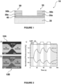
- Figure 1 shows a schematic representation of a photodetector 10 for use in discriminating between wavelength regions in an electromagnetic spectrum, according to a preferred embodiment of the present invention.
- the photodetector 10 includes an electrically insulating substrate 20, a pair of terminal electrodes 30, 35 patterned on a surface of the substrate 20 in the Drain-Source configuration (along the armchair direction) in mutually spaced apart and opposing relation, and a sensing element 40 supported on the same surface of the substrate 20, between and in electrical contact with the pair of terminal electrodes 30, 35.
- the first terminal electrode 30 takes the form of a drain contact and includes a first layer 30a of metal (such as Cr, Ti, Al) and a second layer 30b of metal (such as Au, Pt, Pd, Ni), each deposited using a suitable metal deposition method.
- a first layer 30a of metal such as Cr, Ti, Al
- a second layer 30b of metal such as Au, Pt, Pd, Ni
- the second terminal electrode 30 takes the form of a source contact and includes a first layer 35a of metal (such as Cr, Ti, Al) and a second layer 35b of metal (such as Au, Pt, Pd, Ni), each deposited using a suitable metal deposition method.
- a first layer 35a of metal such as Cr, Ti, Al
- a second layer 35b of metal such as Au, Pt, Pd, Ni
- the sensing element 40 takes the form of a few-layer thin black phosphorous (BP) flake that has been mechanically exfoliated by sticking an adhesive tape onto the BP bulk crystal and peeling off a small amount of material.
- the BP micro-flake produced as a result of the exfoliation is then transferred directly onto the surface of the insulating substrate 20.
- the inventors have found that good results can be achieved when the mechanically exfoliated BP micro flake is comprised of one or more layers of black phosphorus, where the resultant BP micro flake has a thickness greater than about 3 nm, and a lateral dimension greater than about 1 ⁇ m.
- the BP micro-flake was found to have a bandgap of greater than 0.2 electron volts.
- the substrate 20 used may be manufactured from a material selected from any one or more of the following group of materials consisting of glass, oxide, silicon, ceramic, a polymer.
- the BP photodetector includes a substrate 20 that takes the form of an oxide coated silicon (SiO 2 /Si) substrate as a semiconducting material.
- This particular BP photodetector for quantitatively discriminating between different wavelength regions of the electromagnetic spectrum is hereinafter referenced as 10A.
- the inventors have surprisingly found that the BP photodetector 10 shows a remarkable propensity for quantitatively discriminating between the wavelength regions associated with the UV-A (315 nm to 400 nm) and UV-B (280 nm to 315 nm) components associated with sunlight.
- Figure 2c shows a plot presenting the current vs time characteristics of the fabricated BP photodetector 10A when acquired at a constant DC voltage of 50 mV under individual cycles of UV-B (280 nm) and UV-A (365 nm) illuminations. It is seen that while the current increases on exposure to 280 nm, it shows an opposite (decreasing) trend on being irradiated with 365 nm wavelength. This observation of opposing trends for the UV-B (280 nm) and UV-A (365 nm) shows that the few-layer thin BP based photodetector 10A can discriminate between the two types of UV radiation.
- the photocurrent exhibits a dependence on the incident power density of the UV-B and UV-A emissions impinging on the BP micro-flake sensing element 40.
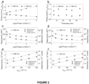
- Figure 3a shows a plot of power-dependent normalised photocurrent ( I Light / I Dark ) as a function of UV-B and UV-A illumination power density ranging from 0.1 mWcm -2 to 3 mWcm -2 .
- Solid lines correspond to the linear fitting of the experimental data for UV-B (280 nm) illumination (open circles) and UV-A (365 nm) illumination (open triangles).
- the photocurrent shows a positive dependence on the power density, which can be attributed to the higher number of photo-generated carriers under ⁇ 4.4 eV (280 nm) excitation energy relative to the number of photo-generated carriers under ⁇ 3.4 eV (365 nm). While under UV-A (365 nm) illumination, the photocurrent shows a negative dependence on the illumination power density.
- Figure 3b shows a plot of normalised photocurrent ( I Light / I Dark ) as a function of the BP flake thickness (nm) selected for the BP photodetector 10A. It is apparent that under a constant UV-B/UV-A illumination power density, the photocurrent is independent of the thickness of the BP micro-flake across a range of thicknesses ranging from ⁇ 5 nm to ⁇ 45 nm. This highlights the significant technological relevance that the BP micro-flake sensing element 40 can effectively sense and discriminate UV-B and UV-A irradiation regardless of the crystal thickness.
- the performance of the BP photodetector 10A is quantitatively assessed by calculating important figures-of-merit, including responsivity ( R ), external quantum efficiency (EQE ) and specific detectivity (D*) for both UV-B and UV-A wavelengths.
- Figures 3c and 3d present the power-dependent responsivity (AW -1 ) and detectivity under UV-B (280 nm) and UV-A (365 nm) illumination wavelengths, respectively.
- the observed decrease in responsivity (AW -1 ) and detectivity with increasing power density (mWcm -2 ) for both illumination wavelengths is consistent with that reported for conventional photodetectors.
- FIGS. 3e and 3f show the Drain-Source bias ( V DS ) dependent responsivity and specific detectivity under UV-B (280 nm) and UV-A (365 nm) illuminations, respectively, at a fixed power density of 0.4 mWcm -2 .
- V DS drain to source voltage
- the BP micro-flake sensing element 40 has a responsivity that falls within a range of 4.8 ⁇ 10 4 A/W to 4.9 ⁇ 10 4 A/W when subjected to UV-B (280 nm) irradiation at an intensity of 1 mW/cm 2 , and a responsivity that falls within a range of 3.1 ⁇ 10 5 A/W to 3.2 ⁇ 10 5 A/W when subjected to UV-B (280 nm) irradiation at an intensity of 0.1 mW/cm 2 .
- the BP micro-flake sensing element 40 has a responsivity that falls within a range of 1.6 ⁇ 10 4 A/W to 1.7 ⁇ 10 4 A/W when subjected to UV-A (365 nm) irradiation at an intensity of 1 mW/cm 2 , and a responsivity that falls within a range of 7.7 ⁇ 10 4 A/W to 7.8 ⁇ 10 4 A/W when subjected to UV-A (365 nm) irradiation at an intensity of 0.1 mW/cm 2 .
- a maximum responsivity of 3.2 ⁇ 10 5 AW -1 (with corresponding D ⁇ of 2.1 ⁇ 10 13 Jones and EQE of 1.4 ⁇ 10 6 %) is achieved for the photodetector 10A when illuminated with an illumination wavelength of 280 nm under a power density of 0.1 mWcm -2 .
- a maximum responsivity of 7.8 ⁇ 10 4 AW -1 (with corresponding D ⁇ of 5.1 ⁇ 10 12 Jones and EQE of 3.4 ⁇ 10 5 %) is measured for the same photodetector 10A when illuminated with an illumination wavelength of 365 nm under a power density of 0.1 mWcm -2 .
- Figure 4a shows an atomic force microscope (AFM) topographic scan and height profile ( Figure 4b ) of ca. 5.7 nm BP flake (corresponding to 10 layers) selected for a representative device on a SiO 2 /Si substrate ( Figure 4c ).
- AFM atomic force microscope
- Figure 4b Two pairs of metal electrodes are orthogonally patterned on the selected BP flakes, where an electrode pair (A-B) is patterned along x-direction ( armchair) and another electrode pair (C-D) along y -direction ( zigzag ).
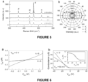
- the BP crystal orientation is identified by the polarization-resolved Raman spectroscopy ( Figure 4d ), where the ratio of the A g 2 and A g 1 peak intensity is higher ( ⁇ 3.51 ⁇ 0.02) along x-direction than y-direction ( ⁇ 1,35 ⁇ 0.03).
- the crystal orientation of mechanically exfoliated few-layer black phosphorus (BP) flakes is assessed by polarization-dependent Raman spectroscopy and electric field dependent carrier mobility measurements.
- Figure 5a shows representative polarization-dependent Raman spectra of a ⁇ 5.7 nm thin BP flake with excitation laser polarized aligned at different angles, ranging between 0° (x-direction) and 90° (y-direction).
- Figure 5b shows a polar plot of peak intensities A g 1 , A g 2 and B g 2 modes corresponding to polarization angles.
- Figure 6b shows conductance and transfer characteristics (inset) along A-B and C-D electrode pairs as a function of gate voltage.
- the on-off current ratios are exceeding 10 3 along both electrode pairs.
- field dependent carrier mobilities of ca. 166 cm 2 V -1 s -1 and ca. 95 cm 2 V -1 s -1 are extracted along A-B and C-D electrode pairs, respectively.
- Transient photoresponse of the representative device is acquired in the UV region of the light spectrum and along both electrode pairs at a constant DC bias of 50 mV.
- UV-B 280 nm
- Figure 8 and Figure 9 show atomic and band structures of oxidised and reduced phosphorene structures, respectively, along with their formation energies (E f ).
- the monolayer phosphorene structure is constructed from 4 ⁇ 6 replicas of a phosphorene unit cell. Density-functional theory (DFT) calculations are performed to optimize the atomic structures, and then subsequently to calculate the band structures and formation energies of these structures.
- DFT Density-functional theory
- E f E Defect + O ⁇ E Defect + nE O + mE H , where E Defect+o is the total energy of the oxidised defective system, E Defect is the total energy of the unoxidized defective phosphorene, n is the number of added O atoms, E O is half of the total energy of the oxygen molecule, m is the number of added H atoms, and E H is half of the total energy of the hydrogen molecule.
- the calculated formation energies are generally negative because oxidation or reduction stabilises the defective structure.
- Figure 7a shows the atomic structure of phosphorene after introducing an oxygen atom into the defective structure. While, Figure 7c shows an oxidised structure (as in Figure 7a ) stacked on two pristine phosphorene layers to form a trilayer structure.
- the localisation of a defect level is indicated by the dispersiveness of the defect energy; that is, if the level in the band structure is a straight line, the defect will be spatially localised.
- the band structure of an oxidised phosphorene structure in Figure 7b induced by incorporating an oxygen atom, shows a nearly straight defect level which suggests that it is nearly localised. Furthermore, the defect levels induced in different oxidised structures are also nearly localised.
- the energy-dispersive X-ray spectroscopy (EDS) and electron energy loss spectroscopic (EELS) analysis of the BP flakes show oxidation of as-exfoliated BP flakes and presence of a phosphorus-oxide (PO x ) layer on the BP flakes.
- EDS energy-dispersive X-ray spectroscopy
- EELS electron energy loss spectroscopic
- TEM transmission electron microscopy
- Figure 10a shows a cross-sectional TEM micrograph of a representative BP device with a structure of Au/Cr/BP/SiO 2 /Si where Au/Cr layers are patterned as electrical contacts.
- High-resolution TEM reveals the presence of ⁇ 3 nm amorphous layers at the top Cr/BP and bottom BP/SiO 2 interfaces.
- the composition of these amorphous layers is identified by acquiring EELS O- K edge and P- L edge area maps ( Figure 10b ) of a region-of-interest (ROI), highlighted by an enclosed area in Figure 10a .
- the EELS area maps show oxygen content at the interfacial regions associated to the amorphous layers, indicating the presence of phosphorus oxide at the top and bottom interfaces of the BP device. Furthermore, the presence of oxygen content in the Cr layer can be attributed to the partial oxidation of Cr to chromium oxide during device fabrication.
- Figure 10e shows a quantitative EDS comparison of a representative BP flake before and after thermal treatment at 150 °C in Ar for 60 min.
- the normalized X-ray energy spectra and EDS area maps show that annealing in an inert Ar environment reduces oxygen content from 3.1 wt% to 0.9 wt% which is expected to be from the surface of BP flake.
- the presence of residual oxide observed after thermal treatment can be explained by the formation of a stable phase of phosphorus oxide (such as P 2 O 5 ) as reported in the literature.
- Figure 11a shows UV-IR optical absorbance spectra of an ambient exposed BP flake and after thermal annealing in argon at 150 °C for 1 hour.
- a comparative change in the spectra after thermal annealing can be associated with the evaporation of surface adsorbates on BP.
- AFM scans of a BP flake show improved surface morphology with ⁇ 31% reduction in average surface roughness after thermal annealing of the flake ( Figure 11b and Figure 11c ).
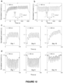
- Figure 12a and Figure 12b show cyclic endurance of a BP device for 10 3 illumination cycles of 280 nm and 365 nm wavelengths, respectively.
- the BP devices (five different devices test for endurance tests) show stable switching performance without any significant decay in photoresponse.
- the time stability of BP devices is evaluated over 16 days ( Figure 12c and Figure 12d ). Devices show a slight change in the magnitude of photocurrent after 8 days. However, a significant change in the photocurrent is observed after 16 days which can be attributed to the partial degradation of BP flake leading to poor electrical conduction and photoresponse.
- FIG. 13a and Figure 13b shows that the BP device retains a positive and negative photoresponse under 280 nm and 365 nm wavelengths, respectively, after surface treatment with [BMIM][BF 4 ].
- a small drop ( ⁇ 3%) in the photoresponse after treatment can be associated with the absorbance of [BMIM][BF 4 ] in UV region ( Figure 13c ).
- Figure 14a shows a scanning transmission electron microscopy (STEM) micrograph of mechanically exfoliated BP on a lacey carbon grid.
- STEM scanning transmission electron microscopy
- the layered structure of BP can be clearly observed from color contrast of the representative flake.
- Chemical purity of the exfoliated BP is inspected by corresponding elemental energy dispersive spectroscopy (EDS) area maps of phosphorus and oxygen as shown in Figure 14b and 14c , respectivley.
- Comparative EDS elemental maps show oxygen signals on the BP which can be associated with oxygen absorption on the surface during sample preparation and exposure to the ambient environment.
- the electron energy loss spectroscopy (EELS) spectra collected from a point on the BP flake are analysed to access oxygen adsoption on the BP.
- the core-loss P- L edge and O- K edge EELS spectra shown in Figure 14d and Figure 14e respectivley, further confirms the surface oxidation of the representative BP flake.
- the photoresponse of BP photodetectors is measured under a wide range of illumination wavelengths, covering UV-C (254 nm), UV-B (280 nm and 305 nm), UV-A (365 nm) and visible (455 nm) bands in the electromagnetic spectrum.
- Figure 15a shows the excitation with shorter UV wavelengths ( ⁇ 302 nm, UV-B and UV-C) results in positive photoresponse.
- a negative photoresponse is observed under the illumination of 365 nm (UV-A) and 455 nm (visible) wavelengths ( Figure 15b ).
- the difference in the magnitude of photocurrent under illumination, under a fixed power density (1 mW/cm 2 ) can be associated with the photon energy of the excitation wavelengths. Furthermore, the measured positive photocurrent under wavelengths with high photon energy ( ⁇ 4.1 eV) and negative photocurrent under wavelengths with low photon energy ( ⁇ 3.39 eV) is consistent with the DFT simulations shown in Figure 7 .
- transient photocurrent is measured as function of varying incident power ranging between 100 ⁇ W/cm 2 and 1.5 mW/cm 2 .
- Figure 16 shows that BP is sensitive to the incident power density of both UV-B ( Figure 16a ) and UV-A ( Figure 16b ).
- Transient photocurrent of a BP device under a short pulse (100 ms) of UV-A (365 nm) and UV-B (280 nm) illumination wavelengths are shown in Figure 17a and 17b , respectively.
- the recovery/fall time for both excitation wavelengths are measured between 10-90% of the photocurrent.
- UV-A illumination is turned off, photocurrent recovers back to 10% margin in ⁇ 7 s whereas it takes ⁇ 93 s after UV-B excitation. This indicates that the BP devices described herein exhibit a persistent photocurrent under 280 nm excitation wavelength.
- Scalable optoelectronic devices capable of performing logic computation with optical signals are highly desired for future applications because light renders ultrafast computational speed due to high bandwidth, low crosstalk and ultralow power-consumption.
- it is possible to exploit the opposing-polarity photoresponse of few-layer BP under different UV wavelengths to demonstrate an optoelectronic logic element.
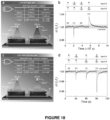
- Figure 18a shows a schematic illustration of an integrated 2-bit optoelectronic exclusive OR (XOR) logic gate where 365 nm and 280 nm wavelengths act as Input A and Input B, respectively, for two serially connected BP devices.
- XOR exclusive OR
- Output output digital states
- ⁇ I change in output current
- the conditions for both optical inputs are set to induce similar magnitude of ⁇ I as stated in the inset of Figure 18a .
- Figure 18c shows a schematic illustration of a 2-bit optoelectronic OR/ADDER logic operation where the binary optical input signals are added to provide an output that is an analog equivalent to the digital sum.
- Figure 18d shows the time trace of ⁇ I for OR/ADDER logic operation for different input configurations where same 365 nm wavelength is illuminated for both Input A and Input B. Interestingly, magnitude of the photoresponse almost doubles when both inputs are High which can be associated with the summation of photogenerated charge carriers.
- OR/ADDER logic operation can also be performed by illuminating 280 nm wavelength as Input A and Input B.
- the high-fidelity optical OR/ADDER logic operation can be extended to perform more complex operations (such as an optoelectronic digital-to-analog convertor) by fabricating multiple integrated devices.
- BP devices exhibit a positive photoresponse under shorter UV wavelengths ( ⁇ 302 nm) and a negative photoresponse under longer UV and visible wavelengths (365 nm and 455 nm, respectively), the selection of any two wavelengths for an application can result in comparatively different magnitudes of photocurrent without affecting the capability to execute that application.
- the magnitude of photocurrent is higher for polarized light along armchair direction than zigzag. As such, regardless of the light's polarization direction the capability of these BP devices to exhibit a unique combination of positive and negative photoresponse for multifunctional applications remains unchanged.
- a few-layer BP photodetector (hereinafter referenced as10B) configured for discriminating between different wavelength regions of the electromagnetic spectrum, more particularly, to the wavelength regions associated with the UV-A (315 nm to 400 nm) and UV-B (280 nm to 315 nm) components of sunlight, has been fabricated on a flexible substrate according to another preferred embodiment of the present invention.
- the inventors have found that by manifesting the flexible UV-B and UV-A discriminating BP photodetector 10B renders its adaptability for various working environments and applications such as flexible and wearable electronics.
- the flexible substrate 20 may be manufactured from any one of a range of suitable polymers including, but not limited to a polymer selected from the group consisting of polyethylene 2,6-naphthalate) (PEN), polyethylene imine (PEI), poly(methyl methacrylate) (PMMA), polyimide (PI), polyethylene terephthalate (PET), and polydimethylsiloxane (PDMS).
- PEN polyethylene 2,6-naphthalate
- PEI polyethylene imine
- PMMA poly(methyl methacrylate)
- PI polyimide
- PET polyethylene terephthalate
- PDMS polydimethylsiloxane
- the flexible substrate 20 used to support the few-layer BP sensing element 40 is manufactured from polyethylene 2,6-naphthalate) (PEN) at a thickness of 125 ⁇ m.
- PEN polyethylene 2,6-naphthalate
- the flexible substrate 20 used to support the few-layer BP sensing element 40 is manufactured from a flexible polyimide (PI) sheet.
- the BP micro-flake sensing element 40 and the pair of terminal electrodes 30, 35 are deposited on the surface of the flexible photodetector 10B using the same process as described above in respect of the photodetector 10A formed on the surface of the SiO 2 /Si substrate.
- this flexible BP photodetector 10B has been evaluated under varying UV-B/UV-A illumination power densities (mWcm 2 ) and different mechanical bending cycles and radii. Similar to the BP photodetector 10A fabricated on a SiO 2 /Si substrate described above, this flexible BP photodetector 10B has also been found to exhibit a power dependent photoresponse.
- Figures 19a and 19b show an illumination power dependent responsivity (AW -1 ) and detectivity results for this representative flexible BP photodetector 10B under UV-B and UV-A irradiation, respectively, when subjected to the corresponding illumination wavelengths (280 nm and 365 nm) with power densities ranging from 0.1 mWcm -2 to 3 mWcm -2 .
- AW -1 illumination power dependent responsivity
- a maximum responsivity of 2.8 ⁇ 10 5 AW -1 and corresponding detectivity of 4.3 ⁇ 10 13 Jones is measured for UV-B (280 nm) illumination under a power density of 0.1 mWcm -2 .
- a maximum responsivity and corresponding detectivity measured for UV-A (365 nm) illumination under a power density of 0.1 mWcm -2 is 3.1 ⁇ 10 4 AW -1 and 4.7 ⁇ 10 12 Jones, respectively.
- Figure 19c shows a power dependent external quantum efficiency (%, EQE) for this representative flexible BP photodetector 10B under UV-B (280 nm; open circles) and UV-A (365 nm; open triangles) irradiation.
- the highest quantum efficiency of 1.2 ⁇ 10 6 % is measured for UV-B excitation under a power density of 0.1 mWcm -2 .
- Figures 19d-19f provide performance results for the flexible BP photodetector 10B (fabricated on a PI substrate) when evaluated under mechanical flexibility conditions.
- Figure 19d shows the normalised photocurrent ( I Light / I Dark ) measured after systematic bending cycles applied by an automatized flexing stage, in which the bending radius was set to ⁇ 3 mm during the automatized bending test.
- the normalised photocurrent ( I Light / I Dark ) measured under both UV-B (280 nm) and UV-A (365 nm) illuminations show negligible variations during 1000 bending cycles with a curvature radii of ⁇ 3 mm.
- the BP micro-flake sensing element 40 of the photodetectors (10, 10A, 10B) described above is responsive to electromagnetic radiation in the UV-A, UV-B wavelength regions to yield a change in photocurrent measured between the terminal electrodes 30, 35 of the photodetector (10, 10A, 10B) as a function of the intensity (mWcm -2 ) of the UV-A and UV-B radiation impinging thereon.
- the inventors have shown that exposure to UV-B (280 nm) irradiation has a positive dependency on the intensity, while exposure to UV-A (365 nm) illumination has a negative dependency on the intensity.
- UV-A/B discriminating photodetectors (10, 10A, 10B) described in herein offers a simple and comparatively easy to fabricate device structure, which offers a cost-effective alternative to currently available technology, which typically require specialized substrates and processes which limit their adoptability for applications.
- the photodetectors (10, 10A, 10B) described above utilize very low operational voltages ( ⁇ 0.2 V) to measure photocurrent produced as a result of UV-A and UV-B illumination wavelengths impinging on the surface of the BP micro-flake sensing element 40 of these as-fabricated photodetectors (10, 10A, 10B).
- ⁇ 0.2 V operational voltages
- %, EQE external quantum efficiency
- the responsivity of 3.2 ⁇ 10 5 A/W and 7.8 ⁇ 10 4 A/W measured for UV-B (280 nm) and UV-A (365 nm) illumination, respectively, are (to the best of the inventors'knowledge) the highest for any UV-B/UV-A discriminating photodetector.
- the photodetectors (10, 10A, 10B) described above can be integrated with CMOS circuits and find wide application in the field of flexible/wearable electronics that can be used to continuously monitor a person's exposure to the harmful UV-A and UV-B rays of sunlight.
- the inventors also believe that these photodetectors (10, 10A, 10B) may also find application in photometry apparatuses, for example photographic exposure meter.
- the inventors Under a constant UV-B/UV-A illumination power density, the inventors have found that the photocurrent is independent of the crystal thickness of the BP micro-flake sensing element 40 used in the as-fabricated photodetectors (10, 10A, 10B) for a range of thicknesses from ⁇ 5 nm to ⁇ 45 nm. This highlights the significant technological relevance that the BP sensing element 40 can effectively sense and discriminate between UV-B (280 nm to 315 nm) and UV-A (365 nm to 315 nm) irradiation regardless of the crystal thickness.
- BP bulk black phosphorus
- PEN polyethylene naphthalate
- PI polyimide
- PET polyethylene terephthalate
- Substrates were cleaned by thoroughly rinsing in acetone, isopropanol (purchased from Sigma-Aldrich) and deionized water, sequentially, for 5 minutes each. Finally, the substrates were blown dry with compressed nitrogen gas.
- BP micro-flakes are produced by applying a piece of adhesive tape onto the surface of the bulk BP crystal and peeling off a small amount of material by mechanical exfoliation. Optical contrast is then used to identify those BP micro-flakes having a thickness that falls within the range of 3 nm to 30 nm.
- the freshly exfoliated BP micro-flakes are then transferred onto the surface of an insulating substrate such as glass, SiO 2 /Si or polymer such as polyethylene naphthalate (PEN), polyimide (PI) and polyethylene terephthalate (PET), where they adhere firmly by virtue of the surface energy of the cleaned substrate surface.
- PEN polyethylene naphthalate
- PI polyimide
- PET polyethylene terephthalate
- Electron beam lithography and photolithography were used to pattern conductive contacts in the form of metal electrodes on the selected BP flakes with different thicknesses ranging from ⁇ 5.7 nm to ⁇ 45 nm. These conductive contacts are defined on the surface of the substrate using thin films of low electrical resistance, which can be any category of metal or conductive metal oxides (such as Cr/Au, Cr/Pt, Ni, Al, indium tin oxide, Al-doped zinc oxide).
- metal electrodes Cr/Au (5/70 nm) and Ti/Au (5/70 nm) were deposited on the developed patterns using electron beam evaporation. These conductive contacts are patterned to be in electrical contact with the BP micro-flake on the substrate surface in two-terminal or four-terminal configurations for the measurement of photocurrent.
- an MA6 mask aligner (Suss MicroTec AG, Germany) was used to pattern a pair of contact electrodes onto the surface of the substrate such that the two patterned electrodes are in electrical contact with the BP micro-flake in mutually spaced apart and opposing relation in the Drain-Source configuration (along the armchair direction).
- Each electrode is formed by using a ProLine75 electron beam evaporator (Kurt J. Lesker Co., USA) to firstly deposit a thin film of a metal such as Cr, Ti, Al onto the surface of the substrate as an adhesion layer, and then subsequently using the same evaporator to deposit a thin film of a second metal such as Au, Pt, Pd, Ni onto the adhesion layer. Finally, the lift-off in acetone was carried out to reveal the required metallic contact pads for micro-probes and electrical measurement.
- a ProLine75 electron beam evaporator Karl J. Lesker Co., USA
- the electrical measurements were conducted using a Keithley 4200SCS semiconductor parameter analyser and Agilent 2912A source meter. All measurements were performed under dark conditions with exposure to only the target illumination wavelengths.
- the photocurrent measurements of the resultant photodetectors were obtained in the probe configuration using a B2912A Precision Source/Measurement Unit (Keysight Technologies, USA). Specifically, commercial UV-A and UV-B light emitting diodes (M365L2 and M280L3, respectively, from Thorlabs, Inc., USA) were used as illumination sources to illuminate the surface of the photodetectors. The illumination power of the UV-A and UV-B LEDs was calibrated using a commercial 818-UV/DB low-power UV-enhanced silicon photodetector (Newport Corporation, USA). The excitation frequency and pulse width of the light sources were controlled by a programmable PCUno microcontroller board.
- AFM topographic scans of the exfoliated BP flakes were conducted on a Dimension-Icon AFM in ScanAsyst mode.
- the Raman spectra were obtained by using a Horiba LabRAM Evolution micro-Raman system equipped with 9 mW, 532 nm laser (0.5 ⁇ m lateral resolution, 0.25 s exposure), and a 50 ⁇ objective.
- BP flakes were transferred onto the lacey carbon grids.
- thin lamellae were prepared by focused ion beam (FIB) using a FEI Scios DualBeam FIBSEM system. Then TEM characterisations were carried out using a JEOL 2100F scanning transmission electron microscope (STEM) with attached Tridium Gatan image filter, operating at 80 kV acceleration voltage.
- STEM scanning transmission electron microscope
- EELS electron energy loss spectroscopy
- the SIESTA code uses basis sets comprised of numerical atomic orbitals, and approximates the atomic potential in terms of Troullier-Martins [42] norm-conserving pseudopotentials.
- the auxiliary basis uses a real-space mesh with a kinetic energy cut-off of 500 Ry, and the basic functions are radially confined using an energy shift of 0.005 Ry.
- the size of the k-points space is 3 ⁇ 3 ⁇ 1 for all structures considered.
- UV-visible absorbance profiles of an ambient exposed BP flake before and after annealing was measured by CRAIC 20/30 XL UV-Vis micro-spectrophotometer.
- flexible substrate is not limited to PI or PEN as described above, but that other flexible substrates may also be fit for purpose.
- the photodetector for discriminating between wavelength regions associated with UV-A and UV-B components of sunlight are not limited to being formed on a substrate 20 such as SiO 2 /Si, PI or PEN as described above, and that alternative substrates 20 may be used in the fabrication of such photodetectors
- the substrate of the photodetector may be manufactured from a material selected from the group consisting of glass, polyethylene imine (PEI), poly(methyl methacrylate) (PMMA), polyethylene terephthalate (PET), or polydimethylsiloxane (PDMS), as required.
- the substrate may be a glass or SiO 2 /Si substrate that has been coated with one of the above materials.
- anchor as used herein in the specification, should be understood to mean “either or both” of the elements so conjoined, i.e., elements that are conjunctively present in some cases and disjunctively present in other cases. Multiple elements listed with “and/or” should be construed in the same fashion, i.e., “one or more” of the elements so conjoined. Other elements may optionally be present other than the elements specifically identified by the "and / or” clause, whether related or unrelated to those elements specifically identified.
- a reference to "A and/or B", when used in conjunction with open-ended language such as “comprising” can refer, in one embodiment, to A only (optionally including elements other than B); in another embodiment, to B only (optionally including elements other than A); in yet another embodiment, to both A and B (optionally including other elements); etc.
Landscapes
- Physics & Mathematics (AREA)
- Spectroscopy & Molecular Physics (AREA)
- General Physics & Mathematics (AREA)
- Life Sciences & Earth Sciences (AREA)
- Sustainable Development (AREA)
- Light Receiving Elements (AREA)
- Photometry And Measurement Of Optical Pulse Characteristics (AREA)
- Chemical & Material Sciences (AREA)
- Inorganic Chemistry (AREA)
- Engineering & Computer Science (AREA)
- Manufacturing & Machinery (AREA)
Description
- The present invention relates to a sensor and a method for discriminating between wavelength regions in an electromagnetic spectrum using said sensor.
- The invention has been developed primarily for use in discriminating between wavelength regions associated with the UV-A and UV-B components of sunlight, and will be described hereinafter with reference to this application.
- The following discussion of the background to the invention is intended to facilitate an understanding of the invention. However, it should be appreciated that the discussion is not an acknowledgement or admission that any of the material referred to below, and anywhere else in the specification, was published, known or part of the common general knowledge in Australia or any other country as at the priority date of any one of the claims of this specification.
- Light waves from the sun which reach the earth are divided into infrared rays, visible light rays and UV rays on the basis of the region of-the wavelength. In terms of total energy released from the sun, infrared rays comprise 42%, visible light rays comprise 52% and UV rays comprise 6%. However, in terms of the energy of the light, as compared to infrared and visible light rays, UV rays have the larger effect on living organisms.
- In terms of biological effects, UV rays may be categorized into three different types: long wavelength UV rays (UV-A: 315 nm to 400nm), medium wavelength UV rays (UV-B: 280 nm to 315 nm) and short wavelength UV rays (UV-C: 190 nm to 280 nm).
- Atmospheric ozone blocks UV-C and also absorbs a large portion of UV-B. Terrestrial UV light contains approximately 6% of UV-B which causes 80% of harmful effects on humans such as skin cancer, while the remaining 94% of UV-A contributes to the other 20% effects such as retinal damage and immune modulation.
- UV sensors have recently been marketed as a means to conveniently measure the presence or absence and intensity of UV. Conventional UV discriminating sensors utilize photochromic chemicals (
US Patent 5,581,090 andUS Patent 5,387,798 ) and photochemical systems (US Patent 5,028,792 ) which qualitatively indicate the exposure to UV radiation by changing the colour of the device. However, quantification of UV exposure with intensity grading of its discrete component i.e., UV-A and UV-B is required for several applications such as determination of sun protection factor to assess epidermal damage. - Other types of UV sensors based on semiconductor materials such as silicon (
US Patent 20060038249 A1 andUS Patent 8,872,159 ) and group III-V compounds (for example nitride semiconductors,US Patent 20130099249 A1 ) utilize photodiode and phototransistors for the detection of light radiation. However, such UV sensors require specific semiconducting substrates and formation of respective junctions via precise doping and multi-layered structures of the semiconducting materials. As such, this increases the manufacturing cost, limits the choice of substrate and incompatibility with the flexible/wearable electronics. - As such, there is an increasing demand for an inexpensive, portable and wearable (preferably flexible) personal UV sensor or dosimeter than can not only detect UV-A and UV-B exposure, but can also quantify the UV-A and UV-B exposure.
-
US2018138039 A1 andCN105742394 A disclose photodetectors with a black phosphorus thin film. - "Photothermal Effect Induced Negative Photoconductivity and High Responsivity in Flexible Black Phosphorus Transistors.", Miao Jinshui et al., ACS Nano 2017, 11, p.6048-6056, describes a phototransistor with black phosphorus and photothermally induced negative photoconductivity.
- The present invention seeks to provide a sensor and a method for discriminating between wavelength regions in an electromagnetic spectrum using said sensor, which will overcome or substantially ameliorate at least some of the deficiencies of the prior art, or to at least provide an alternative.
- According to a first aspect of the present invention, there is provided a sensor for discriminating between wavelength regions in an electromagnetic spectrum, comprising: a substrate; a sensing element supported on a surface of the substrate; and at least one pair of terminal electrodes disposed on the substrate surface in mutually spaced apart and opposing relation, and in electrical contact with the sensing element, wherein the sensing element is responsive to electromagnetic radiation to yield a change in photocurrent measured between the terminal electrodes as a function of an intensity of the electromagnetic radiation impinging thereon, wherein a positive dependency on the intensity corresponds to a first wavelength region and a negative dependency on the intensity corresponds to a second wavelength region, wherein the sensing element comprises at least one black phosphorus flake.
- In one embodiment, the first wavelength region corresponds to wavelengths that fall within a range of 315 nm to 400 nm, and the second wavelength region corresponds to wavelengths that fall within a range of 280 nm to 315 nm.
- In one embodiment, the black phosphorus flake has a bandgap greater than 0.2 electron volts.
- In one embodiment, the black phosphorus flake has a thickness that is greater than about 3 nm.
- In one embodiment, the black phosphorus flake has a lateral dimension that is greater than about 1 µm.
- In one embodiment, the black phosphorus flake comprises a plurality of black phosphorus layers.
- In one embodiment, the black phosphorus flake has a responsivity that falls within a range of 4.8 × 10⁴ A/W to 4.9 × 10⁴ A/W when subjected to UV-B irradiation at an intensity of 1 mW/cm2.
- In one embodiment, the black phosphorus flake has a responsivity that falls within a range of 3.1 × 10⁵ A/W to 3.2 × 10⁵ A/W when subjected to UV-B irradiation at an intensity of 0.1 mW/cm2.
- In one embodiment, the black phosphorus flake has a responsivity that falls within a range of 1.6 × 10⁴ A/W to 1.7 × 10⁴ A/W when subjected to UV-A irradiation at an intensity of 1 mW/cm2.
- In one embodiment, the black phosphorus flake has a responsivity that falls within a range of 7.7 × 10⁴ A/W to 7.8 × 10⁴ A/W when subjected to UV-A irradiation at an intensity of 0.1 mW/cm2.
- In one embodiment, the sensor substrate is an oxide coated silicon substrate.
- In one embodiment, the sensor substrate is a polymer substrate.
- Suitably, the polymer substrate is manufactured from a polymer selected from the group consisting of
polyethylene 2,6-naphthalate) (PEN), polyethylene imine (PEI), poly(methyl methacrylate) (PMMA), polyimide (PI), polyethylene terephthalate (PET), and polydimethylsiloxane (PDMS). - According to a second aspect of the present invention, there is provided a method of discriminating between wavelength regions in an electromagnetic spectrum using a sensor, comprising the steps of: subjecting a sensing element supported on a surface of a substrate of the sensor according to the first aspect to electromagnetic radiation; and detecting a change in photocurrent measured between at least one pair of terminal electrodes formed on the sensor substrate and in electrical contact with the sensing element, as a function of an intensity of the electromagnetic radiation impinging on the sensing element, wherein a positive dependency on the intensity corresponds to a first wavelength region and a negative dependency on the intensity corresponds to a second wavelength region.
- In one embodiment, the first wavelength region corresponds to wavelengths that fall within a range of 315 nm to 400 nm, and the second wavelength region corresponds to wavelengths that fall within a range of 280 nm to 315 nm.
- According to a third aspect of the present invention, there is provided a method of manufacturing a sensor for discriminating between wavelength regions in an electromagnetic spectrum according to the first aspect, comprising the steps of: supporting a sensing element on a surface of a substrate; forming at least one pair of terminal electrodes on the substrate surface in mutually spaced apart and opposing relation, and in electrical contact with the sensing element.
- The sensing element comprises at least one black phosphorus flake.
- In one embodiment, the black phosphorus flake has a bandgap greater than 0.2 electron volts.
- In one embodiment, the black phosphorus flake has a thickness that is greater than about 3 nm.
- In one embodiment, the black phosphorus flake has a lateral dimension that is greater than about 1 µm.
- In one embodiment, the black phosphorus flake comprises a plurality of black phosphorus layers.
- Other aspects of the invention are also disclosed.
- Notwithstanding any other forms which may fall within the scope of the present invention, preferred embodiments of the invention will now be described, by way of example only, with reference to the accompanying drawings in which:
-
Figure 1 shows a schematic representation of a photodetector comprising a few layer black phosphorus (BP) sensing element supported on a SiO2/Si substrate, according to a preferred embodiment of the present invention; -
Figure 2 shows micrographs of (a) the BP photodetector ofFigure 1 (SiO2/Si substrate) and (b) a BP photodetector comprising a few layer black phosphorus sensing element supported on a flexible polyimide (PI) foil substrate; and (c) a plot representing the measured photocurrent (I/I o) obtained when the photodetector ofFigure 1 (SiO2/Si substrate) is exposed over time (s) to UV-B (280 nm) and UV-A (365 nm) illumination wavelengths, each at a power density of 1 mW/cm2; -
Figure 3 shows plots of the photoresponse of the BP photodetector ofFigure 1 , including: (a) Normalised photocurrent (I Light/I Dark) as a function of UV-B and UV-A power densities, ranging from 0.1 mWcm-2 to 3 mWcm-2, in which the solid lines correspond to the linear fitting of the experimental data for UV-B (open circles) and UV-A (open triangles) illuminations; (b) Normalised photocurrent (I Light/I Dark) as a function of BP flake thickness (nm) selected for the BP photodetector; Incident power-dependent responsivity (AW-1; open circles) and detectivity (open triangles) for (c) UV-B and (d) UV-A illuminations, in which the solid lines correspond to the power law fitting of the experimental data; Drain-source voltage dependent responsivity (×105 AW-1; open circles) and detectivity (open triangles) for (e) UV-B and (f) UV-A illuminations, in which the solid lines correspond to the linear fitting of the experimental data; -
Figure 4 shows (a) an atomic force microscopy (AFM) topographic scan of the BP flake selected for a representative BP photonic device, (b) a plot showing the height profile of the BP flake measured along a line depicted on the topographic scan inFigure 4(a) , which corresponds to 5.7 nm, (c) an optical microscopy photograph of the representative BP photonic device fabricated on a rigid SiO2/Si substrate, having two sets of drain-source electrode pairs - namely 'AB' and 'CD', fabricated orthogonally to each other and used for photo-electronic characterisation, (d) a plot depicting the ratio of Raman A g 2 and A g 1 peak intensity as a function of excitation laser polarization angles, and plots showing the normalised transient photocurrent between A-B and C-D electrode pairs measured under pulsating (e) UV-B (λ = 280 nm) and (f) UV-A (λ = 365 nm) illuminations at power densities of 2 mWcm-2 and a constant DC bias of 50 mV; -
Figure 5 shows (a) Raman spectra of a BP flake (~5.7 nm) exfoliated on a SiO2/Si substrate with excitation laser polarization aligned at different angles, (b) a plot showing the peak intensities of the A g 1, A g 2 and B g 2 modes plotted as a function of polarization angles; -
Figure 6 shows (a) a plot showing the I DS vs. V Ds characteristics measured between the A-B and C-D electrode pairs of the representative BP photonic device ofFigure 4 in the dark without gate voltage (V GS = 0 V), and (b) a plot showing the conductance measurement between both electrode pairs as a function of back-gate bias and at a constant drain-source voltage (V DS = 50 mV), where the inset image inFigure 6b shows the transfer characteristics between the A-B and C-D electrode pairs; -
Figure 7 shows a) the atomic structure of defective phosphorene where one P atom is substituted with an O atom, and where the formation energy is calculated to be -2.43 eV per cell, (b) the band structure of oxidised phosphorene corresponding to the structure inFigure 7(a) , (c) the atomic structure of a trilayer system, where the top layer is the defect structure inFigure 7(a) , and (d) the band structure of the trilayer structure inFigure 7(c) ; -
Figure 8 shows the atomic structure of the four oxidised and two reduced monolayer phosphorene structures, in which (a) one P atom is substituted with an O atom, (b) two P atoms are substituted with two O atoms, (c) four P atoms are replaced by two O atoms, (d) two P atoms are replaced with one O atom, (e) four P atoms are replaced by an OH group, and (f) four P atoms are replaced by two OH groups. Formation energies are labelled for each defect structure; -
Figure 9 shows the corresponding band structure of four oxidised and two reduced monolayer phosphorene structures inFigure 8 ; -
Figure 10 shows (a) a cross-sectional transmission electron microscope (TEM) micrograph of a representative BP device taken for the region under an Au/Cr electrode, (b) electron energy loss spectroscopy (EELS) area maps generated for a region of interest highlighted inFigure 10(a) by taking O-K edge and P-L edge intensities of the collected spectra (at each pixel) after pre-edge background subtraction, (c) a normalised photoresponse of a representative BP device under 365 nm illumination measured before and after being subjected to 150°C for 60 minutes in Ar, where the photocurrents are measured under 4 mW/cm2 and 9 mW/cm2 of power density before and after the thermal treatment, respectively, (d) in-situ Raman spectra of a BP flake subjected to ambient temperature and 150 °C for 60 minutes in Ar, and (e) normalized energy-dispersive X-ray spectroscopy (EDS) spectra collected from a BP flake exfoliated on a TEM grid and exposed to ambient temperature and heat treated at 150 °C for 60 minutes in Ar, where both spectra are normalized with phosphorus peak intensities. Inset show EDS area maps of the BP flake used for EDS analysis. Scale bar corresponds to 3 µm; -
Figure 11 shows (a) UV-IR optical absorbance spectra of mechanically exfoliated BP measured before (red line profile) and after (blue line profile) thermal annealing in Ar at 150 °C for 1 hour, topographic AFM scans of a representative BP flake (b) taken before and (c) after annealing, where the lower panels inFigure 11(b) and Figure 11(c) show thickness profiles (~18 nm) before and after thermal treatment, respectively; -
Figure 12 shows plots showing the cyclic endurance of a BP optoelectronic device measured for 103 switching cycles when illuminated under (a) 280 nm and (b) 365 nm, where short optical pulses with a pulse width of 0.5 s, a period of 5 s and a power density of 1 mW/cm2 are illuminated on the device under dark ambient, and a time stability plot of the BP optoelectronic device over the duration of 16 days evaluated by the photocurrent when illuminated under (c) 280 nm and (d) 365 nm; -
Figure 13 shows plots showing the normalised transient photoresponse of a BP device under (a) 280 nm and (b) 365 nm excitation wavelengths before and after treating with [BMIM][BF4] ionic liquid, where surface treatment is carried out by drop-casting the ionic liquid onto the BP device for 45 minutes followed by rinsing in acetonitrile and N2 blow dry, and (c) a UV-visible absorbance profile of [BMIM][BF4]; -
Figure 14 shows (a) a scanning transmission electron microscopy (STEM) image of a mechanically exfoliated BP flake, taken at 80 kV, elemental energy dispersive spectroscopy (EDS) area maps of (b) phosphorus and (c) oxygen collected from the BP flake inFigure 14(a) , and electron energy loss spectroscopy (EELS) spectra of (d) P-L edge and (e) O-K edge corresponding to a selected point highlighted inFigure 14(a) ; -
Figure 15 shows (a) a plot showing the measured current under UV-C (254 nm) and UV-B (280 nm and 302 nm) irradiation pulses with an illumination time of 10 s, a period of 30 s and a fixed power density of 1 mW/cm2, (b) a plot showing the measured current under UV-A (365 nm) and visible (455 nm) illumination pulses with a power density of 1 mW/cm2 and 5 mW/cm2, respectively; -
Figure 16 shows plots showing the time-resolved normalised photocurrent under different power densities of pulsed (a) UV-B (λ = 280 nm) and (b) UV-A (λ = 365 nm) excitation wavelengths; -
Figure 17 shows plots showing (a) the transient photocurrent under 365 nm excitation wavelength, and (b) the transient photocurrent under 280 nm excitation wavelength, where the photocurrent is measured for a short excitation pulse with a pulse width of 100 ms at a constant illumination power density of 1 mWcm-2 and VDS of 50 mV; -
Figure 18 shows (a) a schematic representation of two serially integrated few-layer BP devices on a rigid SiO2/Si substrate for use in performing 2-bit optoelectronic exclusive OR (XOR) logic operation, in which excitation wavelengths of 365 nm and 280 nm with different incident power density are used as optical input signals on Input A and Input B, respectively, thereby inducing a similar magnitude in the change in output current, where the inset table lists conditions for optoelectronic XOR logic operation, while (b) shows a plot that shows the change in output current (ΔI) verses time for different input configurations, where the shaded region represents the current level where output is regarded as Low [0] and is defined in inset table ofFigure 18(a) , and (c) shows a schematic representation of an integrated device performing 2-bit optoelectronic OR/ADDER logic operation, using the same excitation wavelength of 365 nm for Input A and Input B, where the inset table lists conditions for OR/ADDER logic operation, and (d) shows a plot that shows the output response for different Input A-B configurations. In bothFigure 18(a) and Figure 18(b) , the output current is measured under a constant 50 mV bias; and -
Figure 19 shows plots demonstrating the performance of a flexible photodetector comprising a few layer black phosphorus (BP) sensing element fabricated on a PEN substrate, according to another preferred embodiment of the present invention, including: Power-dependent responsivity (AW-1; open circles) and detectivity (open triangles) under (a) UV-B and (b) UV-A illuminations with power densities ranging from 0.1 mWcm-2 to 3 mWcm-2, in which the experimental data is fitted according to the power law (
- It is to be understood that the following description is for the purpose of describing particular embodiments only and is not intended to be limiting with respect to the above description.
- Since the discovery of graphene, two-dimensional materials (2D) have continued to attract increasing attention owing to their fascinating electrical, optical and mechanical properties. The absence of an intrinsic energy gap in graphene reduces its applicability in electronic and optoelectronic systems. Amongst the family of elemental analogues of graphene, layered black-phosphorus (BP) has emerged as a material of interest owing to its high carrier mobility and the presence of a direct bandgap even in its bulk form. Its thickness dependent bandgap ranges from 0.2 eV for the bulk phase to 1.2 eV for a monolayer.
- Without being bound by any one particular theory, the inventors believe that since black phosphorus (BP) possesses strong absorption features in the UV-blue region,[1] and is highly anisotropic, it is expected that BP may find useful application as a photo-detecting material with high responsivity in the UV region. [2-3]
- With this in mind, the present invention is predicated on the finding of a sensor (hereinafter referred to as a photodetector) which utilizes a sensing element in the form few-layer thin black phosphorus (BP) as a semiconducting material for quantitatively discriminating between different wavelength regions in an electromagnetic spectrum. More specifically, the inventors have surprisingly found that the as-fabricated photodetector is capable of discriminating between the wavelength regions associated with the UV-A (315 nm to 400 nm) and UV-B (280 nm to 315 nm) components of sunlight.
-
Figure 1 shows a schematic representation of aphotodetector 10 for use in discriminating between wavelength regions in an electromagnetic spectrum, according to a preferred embodiment of the present invention. - In its simplest form, the
photodetector 10 includes an electrically insulatingsubstrate 20, a pair ofterminal electrodes substrate 20 in the Drain-Source configuration (along the armchair direction) in mutually spaced apart and opposing relation, and asensing element 40 supported on the same surface of thesubstrate 20, between and in electrical contact with the pair ofterminal electrodes - The first
terminal electrode 30 takes the form of a drain contact and includes afirst layer 30a of metal (such as Cr, Ti, Al) and asecond layer 30b of metal (such as Au, Pt, Pd, Ni), each deposited using a suitable metal deposition method. - The second
terminal electrode 30 takes the form of a source contact and includes afirst layer 35a of metal (such as Cr, Ti, Al) and asecond layer 35b of metal (such as Au, Pt, Pd, Ni), each deposited using a suitable metal deposition method. - According to the preferred embodiment, the
sensing element 40 takes the form of a few-layer thin black phosphorous (BP) flake that has been mechanically exfoliated by sticking an adhesive tape onto the BP bulk crystal and peeling off a small amount of material. The BP micro-flake produced as a result of the exfoliation is then transferred directly onto the surface of the insulatingsubstrate 20. - The inventors have found that good results can be achieved when the mechanically exfoliated BP micro flake is comprised of one or more layers of black phosphorus, where the resultant BP micro flake has a thickness greater than about 3 nm, and a lateral dimension greater than about 1 µm. The BP micro-flake was found to have a bandgap of greater than 0.2 electron volts.
- The
substrate 20 used may be manufactured from a material selected from any one or more of the following group of materials consisting of glass, oxide, silicon, ceramic, a polymer. - In one embodiment, and as illustrated in the micrograph in
Figure 2a , the BP photodetector includes asubstrate 20 that takes the form of an oxide coated silicon (SiO2/Si) substrate as a semiconducting material. This particular BP photodetector for quantitatively discriminating between different wavelength regions of the electromagnetic spectrum is hereinafter referenced as 10A. - As described in more detail below, the inventors have surprisingly found that the
BP photodetector 10 shows a remarkable propensity for quantitatively discriminating between the wavelength regions associated with the UV-A (315 nm to 400 nm) and UV-B (280 nm to 315 nm) components associated with sunlight. - In order to systematically evaluate the performance of the
BP photodetector 10A under UV-B (280 nm) and UV-A (365 nm) illuminations, all measurements are carried out through the pair ofterminal electrodes BP photodetector 10A. -
Figure 2c shows a plot presenting the current vs time characteristics of the fabricatedBP photodetector 10A when acquired at a constant DC voltage of 50 mV under individual cycles of UV-B (280 nm) and UV-A (365 nm) illuminations. It is seen that while the current increases on exposure to 280 nm, it shows an opposite (decreasing) trend on being irradiated with 365 nm wavelength. This observation of opposing trends for the UV-B (280 nm) and UV-A (365 nm) shows that the few-layer thin BP basedphotodetector 10A can discriminate between the two types of UV radiation. - It is observed that the photocurrent exhibits a dependence on the incident power density of the UV-B and UV-A emissions impinging on the BP micro-flake sensing
element 40. - For instance,
Figure 3a shows a plot of power-dependent normalised photocurrent (I Light/I Dark) as a function of UV-B and UV-A illumination power density ranging from 0.1 mWcm-2 to 3 mWcm-2. Solid lines correspond to the linear fitting of the experimental data for UV-B (280 nm) illumination (open circles) and UV-A (365 nm) illumination (open triangles). - As shown in
Figure 3a , under UV-B (280 nm) illumination, the photocurrent shows a positive dependence on the power density, which can be attributed to the higher number of photo-generated carriers under ~4.4 eV (280 nm) excitation energy relative to the number of photo-generated carriers under ~3.4 eV (365 nm). While under UV-A (365 nm) illumination, the photocurrent shows a negative dependence on the illumination power density. -
Figure 3b shows a plot of normalised photocurrent (I Light/I Dark) as a function of the BP flake thickness (nm) selected for theBP photodetector 10A. It is apparent that under a constant UV-B/UV-A illumination power density, the photocurrent is independent of the thickness of the BP micro-flake across a range of thicknesses ranging from ~5 nm to ~45 nm. This highlights the significant technological relevance that the BP micro-flake sensingelement 40 can effectively sense and discriminate UV-B and UV-A irradiation regardless of the crystal thickness. - Furthermore, the performance of the
BP photodetector 10A is quantitatively assessed by calculating important figures-of-merit, including responsivity (R), external quantum efficiency (EQE) and specific detectivity (D*) for both UV-B and UV-A wavelengths. The responsivity which quantifies the photocurrent generated per unit power of the excitation wavelength on the effective area of thephotodetector 10A is calculated by:
- where ΔI is the difference between the measured currents with (ILight) and without (I Dark ) illumination, Pλ is the power density and S is the effective area of the
photodetector 10A. The external quantum efficiency defines the number of effective charge carriers generated per incident photon of the excitation wavelength and is calculated by the following equation:
- where h is Plank's constant, ν is the photon frequency and q is the elemental charge. Furthermore, the specific detectivity describes the smallest detectable signal and is calculated by the following equation:


- where B is the electrical bandwidth, NEP is the noise equivalent power and in is the noise current. Among the three possible noise sources that may limit D*, namely shot noise from dark current, thermal and Johnson-Nyquist noise. The shot noise from the dark current can be considered as the main contributor here as the short wavelength UV illuminations and low measurement voltages (10-200 mV) are used in our experiments. [4]
- As such,
Equation 3 can be simplified as:
-
Figures 3c and 3d present the power-dependent responsivity (AW-1) and detectivity under UV-B (280 nm) and UV-A (365 nm) illumination wavelengths, respectively. The observed decrease in responsivity (AW-1) and detectivity with increasing power density (mWcm-2) for both illumination wavelengths is consistent with that reported for conventional photodetectors. [5-6] -
Figures 3e and 3f show the Drain-Source bias (V DS) dependent responsivity and specific detectivity under UV-B (280 nm) and UV-A (365 nm) illuminations, respectively, at a fixed power density of 0.4 mWcm-2. - Regardless of the excitation wavelength, both responsivity and specific detectivity exhibit a linear dependence on the drain to source voltage (VDS) which can be associated with increasing carrier drift velocity with increasing bias. [7] Such VDS dependent responsivity is consistent with photodetectors previously reported in the literature.[8-9]
- The inventors have found that the BP micro-flake sensing
element 40 has a responsivity that falls within a range of 4.8 × 10⁴ A/W to 4.9 × 10⁴ A/W when subjected to UV-B (280 nm) irradiation at an intensity of 1 mW/cm2, and a responsivity that falls within a range of 3.1 × 10⁵ A/W to 3.2 × 10⁵ A/W when subjected to UV-B (280 nm) irradiation at an intensity of 0.1 mW/cm2. - In the case of UV-A (365 nm) illumination, the inventors have found that the BP micro-flake sensing
element 40 has a responsivity that falls within a range of 1.6 × 10⁴ A/W to 1.7 × 10⁴ A/W when subjected to UV-A (365 nm) irradiation at an intensity of 1 mW/cm2, and a responsivity that falls within a range of 7.7 × 10⁴ A/W to 7.8 × 10⁴ A/W when subjected to UV-A (365 nm) irradiation at an intensity of 0.1 mW/cm2. - As disclosed herein, a maximum responsivity of 3.2×10⁵ AW-1 (with corresponding D∗ of 2.1 ×10¹³ Jones and EQE of 1.4×10⁶%) is achieved for the
photodetector 10A when illuminated with an illumination wavelength of 280 nm under a power density of 0.1 mWcm-2. While a maximum responsivity of 7.8×10⁴ AW-1 (with corresponding D∗ of 5.1 ×10¹² Jones and EQE of 3.4×10⁵%) is measured for thesame photodetector 10A when illuminated with an illumination wavelength of 365 nm under a power density of 0.1 mWcm-2. - This observed relatively higher photoresponse (almost an order of magnitude) of the
BP photodetector 10A when illuminated with an illumination wavelength of 280 nm as compared to that when thesame photodetector 10A is illuminated with an illumination wavelength of 365 nm can be attributed to the higher excitation energy supplied by the higher photon energy associated with the shorter illumination wavelength. - In order to characterise the ambipolar optoelectronic properties of few-layer BP, flakes with different thicknesses are selected for fabricating devices (see Materials and Methods section).
Figure 4a shows an atomic force microscope (AFM) topographic scan and height profile (Figure 4b ) of ca. 5.7 nm BP flake (corresponding to 10 layers) selected for a representative device on a SiO2/Si substrate (Figure 4c ). Two pairs of metal electrodes are orthogonally patterned on the selected BP flakes, where an electrode pair (A-B) is patterned along x-direction (armchair) and another electrode pair (C-D) along y-direction (zigzag). Prior to the electrode fabrication, the BP crystal orientation is identified by the polarization-resolved Raman spectroscopy (Figure 4d ), where the ratio of the Ag 2 and Ag 1 peak intensity is higher (~3.51±0.02) along x-direction than y-direction (~1,35±0.03). - A detailed polarization-resolved Raman analysis of the mechanically exfoliated few-layer black phosphorus (BP) flakes is presented below. Furthermore, the anisotropy of the BP crystal is confirmed by the carrier mobility across the electrode pairs and solving low energy k · p Hamiltonian, as discussed below.
- The crystal orientation of mechanically exfoliated few-layer black phosphorus (BP) flakes is assessed by polarization-dependent Raman spectroscopy and electric field dependent carrier mobility measurements.
-
Figure 5a shows representative polarization-dependent Raman spectra of a ~5.7 nm thin BP flake with excitation laser polarized aligned at different angles, ranging between 0° (x-direction) and 90° (y-direction). -
Figure 5b shows a polar plot of peak intensities Ag 1, Ag 2 and Bg 2 modes corresponding to polarization angles. - Drain current vs. drain voltage characteristics (I DS-V DS) acquired between the electrode pairs (without gate voltage, V GS,
Figure 6a ) show higher electrical conductivity between the A-B electrodes than between the C-D electrodes. Furthermore, the field dependent carrier mobility is extracted along both electrode pairs by utilizing the back gate configuration. -
Figure 6b shows conductance and transfer characteristics (inset) along A-B and C-D electrode pairs as a function of gate voltage. The on-off current ratios are exceeding 103 along both electrode pairs. Also field dependent carrier mobilities of ca. 166 cm2V-1s-1 and ca. 95 cm2V-1s-1 are extracted along A-B and C-D electrode pairs, respectively. Owing to the in-plane anisotropic electrical conductance in BP (with a ratio of 1.5),[10] suggests that A-B electrodes are along the armchair direction and C-D electrodes are along the zigzag direction. - Transient photoresponse of the representative device is acquired in the UV region of the light spectrum and along both electrode pairs at a constant DC bias of 50 mV.
Figure 4e and Figure 4f show normalised transient photocurrent under the illumination of pulsating UV-B (λ = 280 nm) and UV-A (λ = 365 nm) excitation wavelengths, respectively, along the electrode pairs A-B and C-D. In more than 15 devices studied in this work, it is consistently observed that while the current increases on exposure to 280 nm, it shows an opposite (decreasing) trend on exposure to 365 nm wavelength. The relatively high photocurrent (ca. 11% for 280 nm and ca. 4% for 365 nm) along the A-B electrode pair than the C-D one can be associated with the in-plane optical anisotropy which allows higher absorption of the incident light in the armchair direction and dichroic photocurrent generation. [10-13] - In 2D systems, negative photoconductivity is typically associated with the bolometric effect.[9,14-17] However, the unusual negative photocurrent observed in BP under longwave UV (365 nm) excitation is intrinsically material-related and is associated with the surface adsorbates. [14, 18] It has previously been determined that BP in ambient conditions readily adsorbs oxygen and forms phosphorus oxide species across the crystal surface which can act as charge trap sites. [1, 18-22] These extrinsic trap sites, act as scattering centres under light illumination and reduce the conductance of the device and, hence, are the origin of negative photocurrent. In contrast, J. Wu et al.[8] previously reported positive photocurrent in BP phototransistors under 330 nm and 370 nm excitation wavelengths, operating under a negative gate voltage (-80 V) and high vacuum. The presence of electric field at BP/substrate interface can lead to the accumulation of photogenerated positively charge carriers (holes) at the interface resulting in an increase in photocurrent (between drain and source) on excitation. To gain an in-depth understanding of the origin of negative photocurrent under 365 nm excitation wavelength, a series of experimental characterisations coupled with density-functional theory (DFT) calculations were used (as discussed below).
- Ambient oxidation of BP has been analysed in several recently reported DFT investigations,[1, 23-28] where oxygen is predicted to spontaneously dissociate on BP, a process that is facilitated with reduction in the number of BP layers. [29] The adsorption of atomic oxygen is reported to have a negative formation energy (Ef),[30] which indicates that the incorporation of oxygen stabilizes some of the phosphorene defects. Of interest to the present work, Ziletti et al. [31] predicted that metastable structures with adsorbed oxygen atoms exhibit localised defect levels. These levels, which are characterised by horizontal discrete levels within the band gap and do not endure significant dispersion, act as charge traps that diminish the conductance of BP under 365 nm illumination. The oxidation of defective BP, which can also be seen as a substitutional doping of BP with oxygen atoms, introduces localised defects in BP.[30] As such, the investigation of oxidized phosphorene was expanded by studying various oxidised structures and the nature of their induced defects. Since the oxygen dissociation reaction on the surface has a low energy barrier and high exothermicity,[25] it is considered that the chemical adsorption of oxygen has occurred on the surface of BP in their simulations.
- In order to find localised defects, a range of monolayer phosphorene structures with different defect structures were investigated.
-
Figure 8 andFigure 9 show atomic and band structures of oxidised and reduced phosphorene structures, respectively, along with their formation energies (Ef). The monolayer phosphorene structure is constructed from 4 × 6 replicas of a phosphorene unit cell. Density-functional theory (DFT) calculations are performed to optimize the atomic structures, and then subsequently to calculate the band structures and formation energies of these structures. The formation energy is calculated according to the formula:
where E Defect+o is the total energy of the oxidised defective system, E Defect is the total energy of the unoxidized defective phosphorene, n is the number of added O atoms, E O is half of the total energy of the oxygen molecule, m is the number of added H atoms, and E H is half of the total energy of the hydrogen molecule. The calculated formation energies are generally negative because oxidation or reduction stabilises the defective structure. -
Figure 7a shows the atomic structure of phosphorene after introducing an oxygen atom into the defective structure. While,Figure 7c shows an oxidised structure (as inFigure 7a ) stacked on two pristine phosphorene layers to form a trilayer structure. The localisation of a defect level is indicated by the dispersiveness of the defect energy; that is, if the level in the band structure is a straight line, the defect will be spatially localised. The band structure of an oxidised phosphorene structure inFigure 7b , induced by incorporating an oxygen atom, shows a nearly straight defect level which suggests that it is nearly localised. Furthermore, the defect levels induced in different oxidised structures are also nearly localised. The localisation of the defect in the monolayer (Figure 7a and Figure 7b ) also persists in the case of the multilayer, as shown in the band structure inFigure 7d . The presence of localized defect levels in the oxidised structures at such low formation energies explain the observed negative photocurrent under 365 nm illumination: exposure to which causes the formation of oxidised defect structures that harbour localised defect levels and creating charge traps. - On the other hand, exposure to 280 nm wavelength light (having an energy of 4.4 eV, which is very close to the energy required to split an H2 molecule), may give rise to a potential mechanism for the onset of photoconduction via the splitting of H2 and H2O molecules in ambient, resulting in passivation of oxygen sites in oxidised phosphorene and hence the introduction of carriers, which could subsequently lead to the photoconductivity within the sample. In addition to the H-reduction, the increase in conductivity under high photon energy (>4 eV) excitation wavelengths can also be explained by the ionization of defects. [32-34] However, further theoretical investigation is required to validate the exact mechanism of reactions taking place under high photon energy irradiations, and this is the subject of ongoing work.
- The energy-dispersive X-ray spectroscopy (EDS) and electron energy loss spectroscopic (EELS) analysis of the BP flakes show oxidation of as-exfoliated BP flakes and presence of a phosphorus-oxide (POx) layer on the BP flakes. To assess the microstructure of POx layer in these BP devices, cross-sectional lamellae are prepared for transmission electron microscopy (TEM) analysis.
-
Figure 10a shows a cross-sectional TEM micrograph of a representative BP device with a structure of Au/Cr/BP/SiO2/Si where Au/Cr layers are patterned as electrical contacts. High-resolution TEM reveals the presence of ~3 nm amorphous layers at the top Cr/BP and bottom BP/SiO2 interfaces. The composition of these amorphous layers is identified by acquiring EELS O-K edge and P-L edge area maps (Figure 10b ) of a region-of-interest (ROI), highlighted by an enclosed area inFigure 10a . The EELS area maps show oxygen content at the interfacial regions associated to the amorphous layers, indicating the presence of phosphorus oxide at the top and bottom interfaces of the BP device. Furthermore, the presence of oxygen content in the Cr layer can be attributed to the partial oxidation of Cr to chromium oxide during device fabrication. - Thermal treatment of 2D materials, including BP, is known to significantly reduce oxidation-related defects due to the evaporation of surface adsorbates. [35-37] Based on this, it is expected that defect engineering by controlled thermal annealing of defective BP in an inert environment may tune the photoresponse of these devices. As such, a comparison was conducted between the photoresponse and material characteristics of thermally treated BP in an inert Ar environment and ambient exposed untreated BP.
Figure 10c shows that an ambient exposed BP device exhibits negative photocurrent under the illumination of 365 nm, which changes to a positive photocurrent after the device is subjected to 150 °C for 60 min in Ar. This can be associated with the evaporation of surface adsorbates and associated reduction in carrier scattering centres during thermal treatment. [35-36] On the other hand, the devices retain a positive photocurrent profile at 280 nm exposure. In-situ Raman spectra (Figure 10d ) of an ambient exposed flake show relatively small and broad peak in 800-900 cm-1 range which is associated with the Raman vibration modes of phosphorus oxide species. [1, 22, 38] The presence of these oxide species is consistent with the cross-sectional transmission electron microscope (TEM) analyses. It is of note that the in-situ Raman spectra of thermally treated BP flakes show significant reduction in the intensity of oxide peaks after annealing in Ar at 150 °C for 60 min. Furthermore, a relative change in the optical absorbance and morphology is observed after the thermal annealing of an ambient exposed BP flake. -
Figure 10e shows a quantitative EDS comparison of a representative BP flake before and after thermal treatment at 150 °C in Ar for 60 min. The normalized X-ray energy spectra and EDS area maps (inset ofFigure 10e ) show that annealing in an inert Ar environment reduces oxygen content from 3.1 wt% to 0.9 wt% which is expected to be from the surface of BP flake. However, the presence of residual oxide observed after thermal treatment can be explained by the formation of a stable phase of phosphorus oxide (such as P2O5) as reported in the literature. [36-39] The above-mentioned DFT simulations and characterizations reveal a vivid picture where localized charge-trap sites induced by the dissociation of surface adsorbates define the conductance of BP based on the illumination energy. In addition, same photoresponse characteristics, i.e., positive photocurrent under 280 nm and negative photoresponse under 365 nm excitation wavelengths, in devices with Cr/Au and Ti/Au electrode junctions further support the discussion that BP is the functional component of photoresponse in these devices. -
Figure 11a shows UV-IR optical absorbance spectra of an ambient exposed BP flake and after thermal annealing in argon at 150 °C for 1 hour. A comparative change in the spectra after thermal annealing can be associated with the evaporation of surface adsorbates on BP. Furthermore, AFM scans of a BP flake show improved surface morphology with ~31% reduction in average surface roughness after thermal annealing of the flake (Figure 11b and Figure 11c ). - The cyclic endurance and stability of the BP optoelectronic devices are evaluated under ambient conditions.
Figure 12a and Figure 12b show cyclic endurance of a BP device for 103 illumination cycles of 280 nm and 365 nm wavelengths, respectively. The BP devices (five different devices test for endurance tests) show stable switching performance without any significant decay in photoresponse. - The time stability of BP devices is evaluated over 16 days (
Figure 12c and Figure 12d ). Devices show a slight change in the magnitude of photocurrent after 8 days. However, a significant change in the photocurrent is observed after 16 days which can be attributed to the partial degradation of BP flake leading to poor electrical conduction and photoresponse. - To protect the BP devices from extensive ambient degradation, the inventors believe that by employing a surface passivation approach utilizing imidazolium-based ionic liquid (such as 1-butyl-3-methylimidazolium tetrafluoroborate, [BMIM][BF4]), the stability of BP devices can be extended beyond 16 days. [38]
Figure 13a and Figure 13b shows that the BP device retains a positive and negative photoresponse under 280 nm and 365 nm wavelengths, respectively, after surface treatment with [BMIM][BF4]. A small drop (<3%) in the photoresponse after treatment can be associated with the absorbance of [BMIM][BF4] in UV region (Figure 13c ). -
Figure 14a shows a scanning transmission electron microscopy (STEM) micrograph of mechanically exfoliated BP on a lacey carbon grid. The layered structure of BP can be clearly observed from color contrast of the representative flake. Chemical purity of the exfoliated BP is inspected by corresponding elemental energy dispersive spectroscopy (EDS) area maps of phosphorus and oxygen as shown inFigure 14b and 14c , respectivley. Comparative EDS elemental maps show oxygen signals on the BP which can be associated with oxygen absorption on the surface during sample preparation and exposure to the ambient environment. The electron energy loss spectroscopy (EELS) spectra collected from a point on the BP flake (highlighted inFigure 14a ) are analysed to access oxygen adsoption on the BP. The core-loss P-L edge and O-K edge EELS spectra, shown inFigure 14d and Figure 14e respectivley, further confirms the surface oxidation of the representative BP flake. - The photoresponse of BP photodetectors is measured under a wide range of illumination wavelengths, covering UV-C (254 nm), UV-B (280 nm and 305 nm), UV-A (365 nm) and visible (455 nm) bands in the electromagnetic spectrum.
Figure 15a shows the excitation with shorter UV wavelengths (≤302 nm, UV-B and UV-C) results in positive photoresponse. Whereas a negative photoresponse is observed under the illumination of 365 nm (UV-A) and 455 nm (visible) wavelengths (Figure 15b ). - In
Figure 15a , the difference in the magnitude of photocurrent under illumination, under a fixed power density (1 mW/cm2) can be associated with the photon energy of the excitation wavelengths. Furthermore, the measured positive photocurrent under wavelengths with high photon energy (≥4.1 eV) and negative photocurrent under wavelengths with low photon energy (≤3.39 eV) is consistent with the DFT simulations shown inFigure 7 . - To assess the effect of illumination power on photoresponse of the BP devices fabricated on SiO2/Si substrate, transient photocurrent is measured as function of varying incident power ranging between 100 µW/cm2 and 1.5 mW/cm2.
Figure 16 shows that BP is sensitive to the incident power density of both UV-B (Figure 16a ) and UV-A (Figure 16b ). - Transient photocurrent of a BP device under a short pulse (100 ms) of UV-A (365 nm) and UV-B (280 nm) illumination wavelengths (at a constant power density of 1 mWcm-2) are shown in
Figure 17a and 17b , respectively. The recovery/fall time for both excitation wavelengths are measured between 10-90% of the photocurrent. When UV-A illumination is turned off, photocurrent recovers back to 10% margin in ~7 s whereas it takes ~93 s after UV-B excitation. This indicates that the BP devices described herein exhibit a persistent photocurrent under 280 nm excitation wavelength. - Scalable optoelectronic devices capable of performing logic computation with optical signals are highly desired for future applications because light renders ultrafast computational speed due to high bandwidth, low crosstalk and ultralow power-consumption. In this context, it is possible to exploit the opposing-polarity photoresponse of few-layer BP under different UV wavelengths to demonstrate an optoelectronic logic element.
-
Figure 18a shows a schematic illustration of an integrated 2-bit optoelectronic exclusive OR (XOR) logic gate where 365 nm and 280 nm wavelengths act as Input A and Input B, respectively, for two serially connected BP devices. In the optical input - electronic output logic devices, output digital states (Output) are defined as the change in output current (ΔI) corresponding to a defined threshold. For XOR logic operation, the conditions for both optical inputs are set to induce similar magnitude of ΔI as stated in the inset ofFigure 18a . The time trace of ΔI for 2-bit XOR operation (Figure 18b ) shows that when both optical inputs are Low [0-0] or High [1-1], the output ΔI does not increase/decrease than the defined threshold and retains a Low-level [0] (depicted by a shaded region and defined in the inset table ofFigure 18a ). On the other hand, the Output ΔI changes the magnitude to High [1] when either of the two inputs is High, exhibiting an optical XOR logic operation. -
Figure 18c shows a schematic illustration of a 2-bit optoelectronic OR/ADDER logic operation where the binary optical input signals are added to provide an output that is an analog equivalent to the digital sum. -
Figure 18d shows the time trace of ΔI for OR/ADDER logic operation for different input configurations where same 365 nm wavelength is illuminated for both Input A and Input B. Interestingly, magnitude of the photoresponse almost doubles when both inputs are High which can be associated with the summation of photogenerated charge carriers. In this integrated device configuration, OR/ADDER logic operation can also be performed by illuminating 280 nm wavelength as Input A and Input B. In the future, the high-fidelity optical OR/ADDER logic operation can be extended to perform more complex operations (such as an optoelectronic digital-to-analog convertor) by fabricating multiple integrated devices. - Since these BP devices exhibit a positive photoresponse under shorter UV wavelengths (≤302 nm) and a negative photoresponse under longer UV and visible wavelengths (365 nm and 455 nm, respectively), the selection of any two wavelengths for an application can result in comparatively different magnitudes of photocurrent without affecting the capability to execute that application. Similarly, due to the intrinsic anisotropic optical absorbance of BP, the magnitude of photocurrent is higher for polarized light along armchair direction than zigzag. As such, regardless of the light's polarization direction the capability of these BP devices to exhibit a unique combination of positive and negative photoresponse for multifunctional applications remains unchanged.
- A few-layer BP photodetector (hereinafter referenced as10B) configured for discriminating between different wavelength regions of the electromagnetic spectrum, more particularly, to the wavelength regions associated with the UV-A (315 nm to 400 nm) and UV-B (280 nm to 315 nm) components of sunlight, has been fabricated on a flexible substrate according to another preferred embodiment of the present invention.
- The inventors have found that by manifesting the flexible UV-B and UV-A discriminating
BP photodetector 10B renders its adaptability for various working environments and applications such as flexible and wearable electronics. - The
flexible substrate 20 may be manufactured from any one of a range of suitable polymers including, but not limited to a polymer selected from the group consisting ofpolyethylene 2,6-naphthalate) (PEN), polyethylene imine (PEI), poly(methyl methacrylate) (PMMA), polyimide (PI), polyethylene terephthalate (PET), and polydimethylsiloxane (PDMS). - In one embodiment, the
flexible substrate 20 used to support the few-layerBP sensing element 40 is manufactured frompolyethylene 2,6-naphthalate) (PEN) at a thickness of 125 µm. - In one other embodiment, and as shown in the micrograph in
Figure 2b , theflexible substrate 20 used to support the few-layerBP sensing element 40 is manufactured from a flexible polyimide (PI) sheet. - It will be appreciated by persons of ordinary skill in the relevant art that the BP micro-flake sensing
element 40 and the pair ofterminal electrodes flexible photodetector 10B using the same process as described above in respect of thephotodetector 10A formed on the surface of the SiO2/Si substrate. - The performance of this
flexible BP photodetector 10B has been evaluated under varying UV-B/UV-A illumination power densities (mWcm2) and different mechanical bending cycles and radii. Similar to theBP photodetector 10A fabricated on a SiO2/Si substrate described above, thisflexible BP photodetector 10B has also been found to exhibit a power dependent photoresponse. - For instance,
Figures 19a and 19b show an illumination power dependent responsivity (AW-1) and detectivity results for this representativeflexible BP photodetector 10B under UV-B and UV-A irradiation, respectively, when subjected to the corresponding illumination wavelengths (280 nm and 365 nm) with power densities ranging from 0.1 mWcm-2 to 3 mWcm-2. - In particular, and as shown in
Figure 19a , a maximum responsivity of 2.8×10⁵ AW-1 and corresponding detectivity of 4.3×10¹³ Jones is measured for UV-B (280 nm) illumination under a power density of 0.1 mWcm-2. While as shown inFigure 19b , a maximum responsivity and corresponding detectivity measured for UV-A (365 nm) illumination under a power density of 0.1 mWcm-2 is 3.1 ×10⁴ AW-1 and 4.7×10¹² Jones, respectively. -
Figure 19c shows a power dependent external quantum efficiency (%, EQE) for this representativeflexible BP photodetector 10B under UV-B (280 nm; open circles) and UV-A (365 nm; open triangles) irradiation. The highest quantum efficiency of 1.2×10⁶% is measured for UV-B excitation under a power density of 0.1 mWcm-2. These figures-of-merit are comparable with the calculated results indicated above for theBP photodetector 10A fabricated on the rigid SiO2/Si substrate. This suggests that the photoconduction mechanism of theBP sensing element 40 under short excitation wavelengths (at least in the UV range) is independent of the type ofsubstrate 20, which is contrary to that reported in the literature in respect of longer excitation wavelengths (near-infrared and above).[9] -
Figures 19d-19f provide performance results for theflexible BP photodetector 10B (fabricated on a PI substrate) when evaluated under mechanical flexibility conditions. - Specifically,
Figure 19d shows the normalised photocurrent (I Light/I Dark) measured after systematic bending cycles applied by an automatized flexing stage, in which the bending radius was set to ~3 mm during the automatized bending test. As shown, the normalised photocurrent (I Light/I Dark) measured under both UV-B (280 nm) and UV-A (365 nm) illuminations show negligible variations during 1000 bending cycles with a curvature radii of ~3 mm. - Furthermore, and as shown in
Figures 19e and 19f , the normalised photocurrents (I Light/I Dark) vs. time (x 10 s) profiles have been recorded under different bending radii for UV-B (Figure 19e ) and UV-A (Figure 19f ) illuminations, in which the data is collected with a V DS of 50 mV. The photocurrents vs. time profiles show no significant deviation when measured on a flat and bent supports. - These results indicate that the
flexible BP photodetector 10B with superior photoresponse and robust mechanical tolerance could be adopted as a sensing component in future sensing and imaging systems such as personal UV protection and wearable electronics. - The inventors have found that the BP micro-flake sensing
element 40 of the photodetectors (10, 10A, 10B) described above is responsive to electromagnetic radiation in the UV-A, UV-B wavelength regions to yield a change in photocurrent measured between theterminal electrodes - By virtue of this observation, the inventors have identified a means by which to discriminate between two different UV wavelength regions of the electromagnetic spectrum.
- The UV-A/B discriminating photodetectors (10, 10A, 10B) described in herein, offers a simple and comparatively easy to fabricate device structure, which offers a cost-effective alternative to currently available technology, which typically require specialized substrates and processes which limit their adoptability for applications.
- The inventors have found that the photodetectors (10, 10A, 10B) described above utilize very low operational voltages (<0.2 V) to measure photocurrent produced as a result of UV-A and UV-B illumination wavelengths impinging on the surface of the BP micro-flake sensing
element 40 of these as-fabricated photodetectors (10, 10A, 10B). Indeed, several figures-of-merit such as responsivity, detectivity and external quantum efficiency (%, EQE) that have been calculated herein to quantify and evaluate the performance of said photodetectors, are clearly better than the corresponding results obtained for a number of convention al sensors on the market. For instance, the responsivity of 3.2×10⁵ A/W and 7.8×10⁴ A/W measured for UV-B (280 nm) and UV-A (365 nm) illumination, respectively, are (to the best of the inventors'knowledge) the highest for any UV-B/UV-A discriminating photodetector. - The inventors believe that the photodetectors (10, 10A, 10B) described above, can be integrated with CMOS circuits and find wide application in the field of flexible/wearable electronics that can be used to continuously monitor a person's exposure to the harmful UV-A and UV-B rays of sunlight. The inventors also believe that these photodetectors (10, 10A, 10B) may also find application in photometry apparatuses, for example photographic exposure meter.
- Under a constant UV-B/UV-A illumination power density, the inventors have found that the photocurrent is independent of the crystal thickness of the BP micro-flake sensing
element 40 used in the as-fabricated photodetectors (10, 10A, 10B) for a range of thicknesses from ~5 nm to ~45 nm. This highlights the significant technological relevance that theBP sensing element 40 can effectively sense and discriminate between UV-B (280 nm to 315 nm) and UV-A (365 nm to 315 nm) irradiation regardless of the crystal thickness. - Commercial bulk black phosphorus (BP) crystals were obtained from Smart-Elements GmbH (Austria) and used without further purification prior to use. Glass and SiO2/Si used as the substrate for the
photodetector 10A were obtained from Silicon Materials Inc. Polymers such as polyethylene naphthalate (PEN), polyimide (PI) and polyethylene terephthalate (PET) used as the substrate for theflexible photodetector 10B were obtained from Sigma-Aldrich. - Substrates were cleaned by thoroughly rinsing in acetone, isopropanol (purchased from Sigma-Aldrich) and deionized water, sequentially, for 5 minutes each. Finally, the substrates were blown dry with compressed nitrogen gas.
- Briefly, few-layer thin black phosphorus (BP) micro-flakes are produced by applying a piece of adhesive tape onto the surface of the bulk BP crystal and peeling off a small amount of material by mechanical exfoliation. Optical contrast is then used to identify those BP micro-flakes having a thickness that falls within the range of 3 nm to 30 nm. The freshly exfoliated BP micro-flakes are then transferred onto the surface of an insulating substrate such as glass, SiO2/Si or polymer such as polyethylene naphthalate (PEN), polyimide (PI) and polyethylene terephthalate (PET), where they adhere firmly by virtue of the surface energy of the cleaned substrate surface.
- Electron beam lithography and photolithography were used to pattern conductive contacts in the form of metal electrodes on the selected BP flakes with different thicknesses ranging from ~5.7 nm to ~45 nm. These conductive contacts are defined on the surface of the substrate using thin films of low electrical resistance, which can be any category of metal or conductive metal oxides (such as Cr/Au, Cr/Pt, Ni, Al, indium tin oxide, Al-doped zinc oxide).
- Specifically, metal electrodes Cr/Au (5/70 nm) and Ti/Au (5/70 nm) were deposited on the developed patterns using electron beam evaporation. These conductive contacts are patterned to be in electrical contact with the BP micro-flake on the substrate surface in two-terminal or four-terminal configurations for the measurement of photocurrent. For instance, in the case of the two-terminal configuration, an MA6 mask aligner (Suss MicroTec AG, Germany) was used to pattern a pair of contact electrodes onto the surface of the substrate such that the two patterned electrodes are in electrical contact with the BP micro-flake in mutually spaced apart and opposing relation in the Drain-Source configuration (along the armchair direction). Each electrode is formed by using a ProLine75 electron beam evaporator (Kurt J. Lesker Co., USA) to firstly deposit a thin film of a metal such as Cr, Ti, Al onto the surface of the substrate as an adhesion layer, and then subsequently using the same evaporator to deposit a thin film of a second metal such as Au, Pt, Pd, Ni onto the adhesion layer. Finally, the lift-off in acetone was carried out to reveal the required metallic contact pads for micro-probes and electrical measurement.
- The electrical measurements were conducted using a Keithley 4200SCS semiconductor parameter analyser and Agilent 2912A source meter. All measurements were performed under dark conditions with exposure to only the target illumination wavelengths. The field dependent carrier mobilities (µ) were extracted from the equation;


- The photocurrent measurements of the resultant photodetectors were obtained in the probe configuration using a B2912A Precision Source/Measurement Unit (Keysight Technologies, USA). Specifically, commercial UV-A and UV-B light emitting diodes (M365L2 and M280L3, respectively, from Thorlabs, Inc., USA) were used as illumination sources to illuminate the surface of the photodetectors. The illumination power of the UV-A and UV-B LEDs was calibrated using a commercial 818-UV/DB low-power UV-enhanced silicon photodetector (Newport Corporation, USA). The excitation frequency and pulse width of the light sources were controlled by a programmable Arduino-Uno microcontroller board.
- AFM topographic scans of the exfoliated BP flakes were conducted on a Dimension-Icon AFM in ScanAsyst mode. The Raman spectra were obtained by using a Horiba LabRAM Evolution micro-Raman system equipped with 9 mW, 532 nm laser (0.5 µm lateral resolution, 0.25 s exposure), and a 50× objective.
- BP flakes were transferred onto the lacey carbon grids. For cross-sectional analysis of BP devices, thin lamellae were prepared by focused ion beam (FIB) using a FEI Scios DualBeam FIBSEM system. Then TEM characterisations were carried out using a JEOL 2100F scanning transmission electron microscope (STEM) with attached Tridium Gatan image filter, operating at 80 kV acceleration voltage. For electron energy loss spectroscopy (EELS) data analysis, power law fits were used for P-L and O-K pre-edge background corrections where the influence of nearby peaks and plural scattering were removed by selecting narrow signal windows.
- To obtain the atomic and electronic structures of the phosphorene, we perform spin-unrestricted DFT calculations with the SIESTA code [40] using the generalized gradient approximation for the exchange-correlation function as developed by Perdew, Burke and Ernzerhof (PBE). [41] The SIESTA code uses basis sets comprised of numerical atomic orbitals, and approximates the atomic potential in terms of Troullier-Martins[42] norm-conserving pseudopotentials. The auxiliary basis uses a real-space mesh with a kinetic energy cut-off of 500 Ry, and the basic functions are radially confined using an energy shift of 0.005 Ry. [40] We allow full atomic relaxation until the forces on the atoms are less than 0.01 eV/A. The size of the k-points space is 3 × 3 × 1 for all structures considered.
- The UV-visible absorbance profiles of an ambient exposed BP flake before and after annealing was measured by
CRAIC 20/30 XL UV-Vis micro-spectrophotometer. - It will be appreciated by those skilled in the relevant art that the choice of flexible substrate is not limited to PI or PEN as described above, but that other flexible substrates may also be fit for purpose.
- For instance, it will be appreciated that the photodetector for discriminating between wavelength regions associated with UV-A and UV-B components of sunlight are not limited to being formed on a
substrate 20 such as SiO2/Si, PI or PEN as described above, and thatalternative substrates 20 may be used in the fabrication of such photodetectors For instance, the substrate of the photodetector may be manufactured from a material selected from the group consisting of glass, polyethylene imine (PEI), poly(methyl methacrylate) (PMMA), polyethylene terephthalate (PET), or polydimethylsiloxane (PDMS), as required. - In an alternative form, the substrate may be a glass or SiO2/Si substrate that has been coated with one of the above materials.
-
- [1]. Ahmed, T.; Balendhran, S.; Karim, M. N.; Mayes, E. L. H.; Field, M. R.; Ramanathan, R.; Singh, M.; Bansal, V.; Sriram, S.; Bhaskaran, M.; Walia, S., Degradation of black phosphorus is contingent on UV-blue light exposure. npj 2D Mater. Appl. 2017, 1 (1).
- [2]. Qiao, J.; Kong, X.; Hu, Z.-X.; Yang, F.; Ji, W., High-mobility transport anisotropy and linear dichroism in few-layer black phosphorus. .
- [3]. Liu, H.; Du, Y.; Deng, Y.; Peide, D. Y., Semiconducting black phosphorus: synthesis, transport properties and electronic applications. Chemical Society Reviews 2015, 44 (9), 2732-2743.
- [4]. Gong, X.; Tong, M.; Xia, Y.; Cai, W.; Moon, J. S.; Cao, Y.; Yu, G.; Shieh, C.-L.; Nilsson, B.; Heeger, A. J., High-detectivity polymer photodetectors with spectral response from 300 nm to 1450 nm. Science 2009, 325 (5948), 1665.
- [5]. Buscema, M.; Groenendijk, D. J.; Blanter, S. I.; Steele, G. A.; van der Zant, H. S.; Castellanos-Gomez, A., Fast and broadband photoresponse of few-layer black phosphorus field-effect transistors. Nano Lett 2014, 14 (6), 3347-52.
- [6]. Huang, M.; Wang, M.; Chen, C.; Ma, Z.; Li, X.; Han, J.; Wu, Y., Broadband Black-Phosphorus Photodetectors with High Responsivity. Adv Mater 2016, 28 (18), 3481-5.
- [7]. Chen, X.; Lu, X.; Deng, B.; Sinai, O.; Shao, Y.; Li, C.; Yuan, S.; Tran, V.; Watanabe, K.; Taniguchi, T.; Naveh, D.; Yang, L.; Xia, F., Widely tunable black phosphorus mid-infrared photodetector. Nat Commun 2017, 8 (1), 1672.
- [8]. Wu, J.; Koon, G. K. W.; Xiang, D.; Han, C.; Toh, C. T.; Kulkarni, E. S.; Verzhbitskiy, I.; Carvalho, A.; Rodin, A. S.; Koenig, S. P.; Eda, G.; Chen, W.; Neto, A. H. C.; Ozyilmaz, B., Colossal ultraviolet photoresponsivity of few-layer black phosphorus. ACS Nano 2015, 9 (8), 8070-8077.
- [9]. Miao, J.; Song, B.; Li, Q.; Cai, L.; Zhang, S.; Hu, W.; Dong, L.; Wang, C., Photothermal effect induced negative photoconductivity and high responsivity in flexible black phosphorus transistors. ACS Nano 2017, 11 (6), 6048-6056.
- [10]. F. Xia, H. Wang, Y. Jia, Nat. Commun. 2014, 5, 4458.
- [11]. V. Tran, R. Soklaski, Y. Liang, L. Yang, Phys. Rev. 8 2014, 89, 235319.
- [12]. N. Mao, J. Tang, L. Xie, J. Wu, B. Han, J. Lin, S. Deng, W. Ji, H. Xu, K. Liu, L. Tong, J. Zhang, J. Am. Chem. Soc. 2016, 138, 300.
- [13]. H. Yuan, X. Liu, F. Afshinmanesh, W. Li, G. Xu, J. Sun, B. Lian, A. G. Curto, G. Ye, Y. Hikita, Z. Shen, S. C. Zhang, X. Chen, M. Brongersma, H. Y. Hwang, Y. Cui, Nat. Nanotechnol. 2015, 10, 707.
- [14]. C. Biswas, F. Gunes, D. L. Duong, S. C. Lim, M. S. Jeong, D. Pribat, Y. H. Lee, Nano Lett. 2011, 11, 4682.
- [15]. L. Huang, W. C. Tan, L. Wang, B. Dong, C. Lee, K. W. Ang, ACS Appl. Mater. Interfaces 2017, 9, 36130.
- [16]. S. Liu, N. Huo, S. Gan, Y. Li, Z. Wei, B. Huang, J. Liu, J. Li, H. Chen, J. Mater. .
- [17]. J. Y. Wu, Y. T. Chun, S. Li, T. Zhang, J. Wang, P. K. Shrestha, D. Chu, Adv. Mater. 2018, 30, 1705880.
- [18]. K. L. Utt, P. Rivero, M. Mehboudi, E. O. Harriss, M. F. Borunda, A. A. Pacheco SanJuan, S. Barraza-Lopez, ACS Cent. Sci. 2015, 1, 320.
- [19]. J. D. Wood, S. A. Wells, D. Jariwala, K.-S. Chen, E. Cho, V. K. Sangwan, X. Liu, L. J. Lauhon, T. J. Marks, M. C. Hersam, Nano Lett. 2014, 14, 6964.
- [20]. S. Kuriakose, T. Ahmed, S. Balendhran, V. Bansal, S. Sriram, M. Bhaskaran, S. Walia, 2D Mater. 2018, 5, 032001.
- [21]. A. Favron, E. Gaufres, F. Fossard, A. L. Phaneuf-L'Heureux, N. Y. Tang, P. L. Levesque, A. Loiseau, R. Leonelli, S. Francoeur, R. Martel, Nat. Mater. 2015, 14, 826.
- [22]. S. Walia, Y. Sabri, T. Ahmed, M. R. Field, R. Ramanathan, A. Arash, S. K. Bhargava, S. Sriram, M. Bhaskaran, V. Bansal, S. Balendhran, 2D Mater. 2017, 4, 015025.
- [23]. W. Gaoxue, J. S. William, P. Ravindra, P. K. Shashi, 2D Mater. 2016, 3, 025011.
- [24]. A. Ziletti, A. Carvalho, P. E. Trevisanutto, D. K. Campbell, D. F. Coker, A. H. Castro Neto, Phys. Rev. B 2015,91, 085407.
- [25]. A. Ziletti, A. Carvalho, D. K. Campbell, D. F. Coker, A. H. Castro Neto, Phys. Rev. Lett. 2015, 114, 046801.
- [26]. P. Srivastava, K. P. S. S. Hembram, H. Mizuseki, K.-R. Lee, S. S. Han, S. Kim, J. Phys. Chem. C 2015, 119, 6530.
- [27]. J. Lu, J. Wu, A. Carvalho, A. Ziletti, H. Liu, J. Tan, Y. Chen, A. H. Castro Neto, B. Ozyilmaz, C. H. Sow, ACS Nano 2015, 9, 10411.
- [28]. D. W. Boukhvalov, A. N. Rudenko, D. A. Prishchenko, V. G. Mazurenko, M. I. Katsnelson, Phys. Chem. Chem. Phys. 2015, 17, 15209.
- [29]. T. Ahmed, S. Balendhran, M. N. Karim, E. L. H. Mayes, M. R. Field, R. Ramanathan, M. Singh, V. Bansal, S. Sriram, M. Bhaskaran, S. Walia, npj 2D Materials and .
- [30]. P. Srivastava, K. P. S. S. Hembram, H. Mizuseki, K.-R. Lee, S. S. Han, S. Kim, The Journal of Physical Chemistry C 2015, 119, 6530.
- [31]. A. Ziletti, A. Carvalho, D. K. Campbell, D. F. Coker, A. H. Castro Neto, Phys Rev Lett 2015, 114, 046801.
- [32]. D. Wang, D. Han, X. B. Li, S. Y. Xie, N. K. Chen, W. Q. Tian, D. West, H. B. Sun, S. B. Zhang, Phys. Rev. Lett. 2015, 114, 196801.
- [33]. D. Wang, D. Han, D. West, N.-K. Chen, S.-Y. Xie, W. Q. Tian, V. Meunier, S. Zhang, X.-B. Li, npj Comput. Mater. 2019, 5.
- [34]. D. Wang, X.-B. Li, D. Han, W. Q. Tian, H.-B. Sun, .
- [35]. C. Elbadawi, R. T. Queralt, Z.-Q. Xu, J. Bishop, T. Ahmed, S. Kuriakose, S. Walia, M. Toth, I. Aharonovich, C. J. Lobo, ACSAppl. Mater. .
- [36]. S. Yang, A. Kim, J. Park, H. Kwon, P. T. Lanh, S. Hong, K. J. Kim, J. W. Kim, Appl. Surf. Sci. 2018, 457, 773.
- [37]. S. Fan, H. Hei, C. An, W. Pang, D. Zhang, X. Hu, S. Wu, J. Liu, J. Mater. Chem. C2017, 5, 10638.
- [38]. S. Walia, S. Balendhran, T. Ahmed, M. Singh, C. El-Badawi, M. D. Brennan, P. Weerathunge, M. N. Karim, F. Rahman, A. Rassell, J. Duckworth, R. Ramanathan, G. E. Collis, C. J. Lobo, M. Toth, J. C. Kotsakidis, B. Weber, M. Fuhrer, J. M. Dominguez-Vera, M. J. S. Spencer, I. Aharonovich, S. Sriram, M. Bhaskaran, V. Bansal, Adv. Mater. 2017, 29, 1700152.
- [39]. M. H. Jeong, D. Kwak, H. S. Ra, A. Y. Lee, J. S. Lee, ACS Appl. Mater. .
- [40]. M. S. José, A. Emilio, D. G. Julian, G. Alberto, J. Javier, O. Pablo, S.-P. Daniel, J. Phys.: Condens. .
- [41]. J. P. Perdew, K. Burke, M. Ernzerhof, Phys. Rev. Lett. 1996, 77, 3865.
- [42]. N. Troullier, J. Martins, Solid State Comm. 1990, 74, 613.
- Whenever a range is given in the specification, for example, a temperature range, a time range, or concentration range, all intermediate ranges and subranges, as well as all individual values included in the ranges given are intended to be included in the disclosure. It will be understood that any subranges or individual values in a range or subrange that are included in the description herein can be excluded from the claims herein.
- All definitions, as defined and used herein, should be understood to control over dictionary definitions, definitions in documents incorporated by reference, and/or ordinary meanings of the defined terms.
- Throughout this application, the term "about" is used to indicate that a value includes the inherent variation of error for the device, the method being employed to determine the value, or the variation that exists among the study subjects.
- The indefinite articles "a" and "an," as used herein in the specification, unless clearly indicated to the contrary, should be understood to mean "at least one."
- The phrase "anchor," as used herein in the specification, should be understood to mean "either or both" of the elements so conjoined, i.e., elements that are conjunctively present in some cases and disjunctively present in other cases. Multiple elements listed with "and/or" should be construed in the same fashion, i.e., "one or more" of the elements so conjoined. Other elements may optionally be present other than the elements specifically identified by the "and/or" clause, whether related or unrelated to those elements specifically identified. Thus, as a non-limiting example, a reference to "A and/or B", when used in conjunction with open-ended language such as "comprising" can refer, in one embodiment, to A only (optionally including elements other than B); in another embodiment, to B only (optionally including elements other than A); in yet another embodiment, to both A and B (optionally including other elements); etc.
- Spatially relative terms, such as "inner," "outer," "beneath," "below," "lower," "above," "upper," and the like, may be used herein for ease of description to describe one element or feature's relationship to another element(s) or feature(s) as illustrated in the Figures. Spatially relative terms may be intended to encompass different orientations of the device in use or operation in addition to the orientation depicted in the Figures.
- While the invention has been described in conjunction with a limited number of embodiments, it will be appreciated by those skilled in the art that many alternatives, modifications and variations in light of the foregoing description are possible, as long as they fall within the scope of the claims, which define the invention.
- Where the terms "comprise", "comprises", "comprised" or "comprising" are used in this specification (including the claims) they are to be interpreted as specifying the presence of the stated features, integers, steps or components, but not precluding the presence of one or more other features, integers, steps or components, or group thereof.
Claims (16)
- A sensor for discriminating between wavelength regions in an electromagnetic spectrum, comprising:a substrate (20);a sensing element (40) supported on a surface of the substrate (20); andat least one pair of terminal electrodes (30, 35) disposed on the substrate surface (20) in mutually spaced apart and opposing relation, and in electrical contact with the sensing element (40), wherein the sensing element (40) comprises at least one black phosphorous flake, wherein the sensing element (40) is responsive to electromagnetic radiation to yield a change in photocurrent measured between the terminal electrodes (30, 35) as a function of an intensity of the electromagnetic radiation impinging thereon, characterized in that a positive dependency on the intensity corresponds to a first wavelength region and a negative dependency on the intensity corresponds to a second wavelength region.
- A sensor according to claim 1, wherein the first wavelength region corresponds to wavelengths that fall within a range of 315 nm to 400 nm, and the second wavelength region corresponds to wavelengths that fall within a range of 280 nm to 315 nm.
- A sensor according to any one of claims 1, wherein the black phosphorus flake has a bandgap greater than 0.2 electron volts.
- A sensor according to claim 3, wherein the black phosphorus flake has a thickness that is greater than about 3 nm.
- A sensor according to claim 3 or 4, wherein the black phosphorus flake has a lateral dimension that is greater than about 1 µm.
- A sensor according to any one of claims 3 to5, wherein the black phosphorus flake comprises a plurality of black phosphorus layers.
- A sensor according to any one of claims 3 to 6, wherein the black phosphorus flake has a responsivity that falls within a range of 4.8 × 10⁴ A/W to 4.9 × 10⁴ A/W when subjected to UV-B irradiation at an intensity of 1 mW/cm2.
- A sensor according to any one of claims 3 to 6, wherein the black phosphorus flake has a responsivity that falls within a range of 3.1 × 10⁵ A/W to 3.2 × 10⁵ A/W when subjected to UV-B irradiation at an intensity of 0.1 mW/cm2.
- A sensor according to any one of claims 3 to 6, wherein the black phosphorus flake has a responsivity that falls within a range of 1.6 × 10⁴ A/W to 1.7 × 10⁴ A/W when subjected to UV-A irradiation at an intensity of 1 mW/cm2.
- A sensor according to any one of claims 3 to 6, wherein the black phosphorus flake has a responsivity that falls within a range of 7.7 × 10⁴ A/W to 7.8 × 10⁴ A/W when subjected to UV-A irradiation at an intensity of 0.1 mW/cm2.
- A sensor according to any one of claims 8 to 10, wherein the sensor substrate (20) is an oxide coated silicon substrate
- A sensor according to any one of claims 8 to 10, wherein the sensor substrate (20) is a polymer substrate.
- A sensor according to claim 12, wherein the polymer substrate (20) is manufactured from a polymer selected from the group consisting of polyethylene 2,6- naphthalate) (PEN), polyethylene imine (PEI), poly(methyl methacrylate) (PMMA), polyimide (PI), polyethylene terephthalate (PET), and polydimethylsiloxane (PDMS).
- A method of discriminating between wavelength regions in an electromagnetic spectrum using a sensor according to any one of claims 1 to 13, comprising the steps of:subjecting the sensing element (40) supported on the surface of the substrate (20) of the sensor to electromagnetic radiation; anddetecting a change in photocurrent measured between at least one pair of terminal electrodes (30, 35) formed on the sensor substrate (20) and in electrical contact with the sensing element (40), as a function of an intensity of the electromagnetic radiation impinging on the sensing element (40), wherein a positive dependency on the intensity corresponds to a first wavelength region and a negative dependency on the intensity corresponds to a second wavelength region.
- A method according to claim 14, wherein the first wavelength region corresponds to wavelengths that fall within a range of 315 nm to 400 nm, and the second wavelength region corresponds to wavelengths that fall within a range of 280 nm to 315 nm.
- A method of manufacturing a sensor according to any of claim 1 to claim 13 for discriminating between wavelength regions in an electromagnetic spectrum, comprising the steps of:supporting a sensing element (40) on a surface of a substrate (20);forming at least one pair of terminal electrodes (30, 35) on the substrate surface (20) in mutually spaced apart and opposing relation, and in electrical contact with the sensing element (40);wherein the sensing element (40) comprises at least one black phosphorus flake.
Applications Claiming Priority (2)
| Application Number | Priority Date | Filing Date | Title |
|---|---|---|---|
| AU2018902291A AU2018902291A0 (en) | 2018-06-26 | Sensor and method for discriminating between wavelength regions using the sensor | |
| PCT/AU2019/050662 WO2020000037A1 (en) | 2018-06-26 | 2019-06-26 | Sensor and method for discriminating between wavelength regions using the sensor |
Publications (3)
| Publication Number | Publication Date |
|---|---|
| EP3794646A1 EP3794646A1 (en) | 2021-03-24 |
| EP3794646A4 EP3794646A4 (en) | 2022-04-13 |
| EP3794646B1 true EP3794646B1 (en) | 2023-09-20 |
Family
ID=68985325
Family Applications (1)
| Application Number | Title | Priority Date | Filing Date |
|---|---|---|---|
| EP19827313.8A Active EP3794646B1 (en) | 2018-06-26 | 2019-06-26 | Sensor and method for discriminating between wavelength regions using the sensor |
Country Status (5)
| Country | Link |
|---|---|
| US (1) | US11808626B2 (en) |
| EP (1) | EP3794646B1 (en) |
| CN (1) | CN112714962A (en) |
| AU (2) | AU2019295411A1 (en) |
| WO (1) | WO2020000037A1 (en) |
Families Citing this family (3)
| Publication number | Priority date | Publication date | Assignee | Title |
|---|---|---|---|---|
| AU2021379563A1 (en) | 2020-11-10 | 2023-07-06 | Royal Melbourne Institute Of Technology | Systems and methods for data storage and processing |
| WO2023168454A1 (en) * | 2022-03-04 | 2023-09-07 | Central Garden & Pet Company | Photochromic pigment detection to determine uv output intensity of a uv illuminating source within a reptile cage |
| CN117213634B (en) * | 2023-09-15 | 2024-11-12 | 齐鲁工业大学(山东省科学院) | Multidimensional optical information detector and detection method based on two-dimensional Ta2NiSe5 polarization characteristics |
Family Cites Families (11)
| Publication number | Priority date | Publication date | Assignee | Title |
|---|---|---|---|---|
| US8818473B2 (en) * | 2010-11-30 | 2014-08-26 | Covidien Lp | Organic light emitting diodes and photodetectors |
| US9595558B2 (en) * | 2013-11-12 | 2017-03-14 | Intrinsix Corporation | Photodiode architectures and image capture methods having a plurality of photodiode with a shared electrode |
| US9059264B2 (en) * | 2011-09-26 | 2015-06-16 | Drexel University | Tunable hot-electron transfer within a nanostructure |
| WO2014089454A2 (en) * | 2012-12-07 | 2014-06-12 | The Trustees Of Columbia University In The City Of New York | Systems and methods for graphene photodetectors |
| WO2015030528A1 (en) * | 2013-08-30 | 2015-03-05 | 에스케이이노베이션 주식회사 | Gas sensor and method for manufacturing same |
| US10121658B2 (en) * | 2015-05-28 | 2018-11-06 | Korea Research Institute Of Standards And Science | Method of fabricating black phosphorus ultrathin film and black phosphorus ultrathin film thereof |
| WO2017035589A1 (en) * | 2015-09-01 | 2017-03-09 | The University Of Queensland | Narrowband photodetector |
| KR101826052B1 (en) * | 2016-02-18 | 2018-02-06 | 성균관대학교산학협력단 | Method of forming electrodes for electronic device using two dimensional semiconductor and electronic device thereof |
| CN105742394B (en) * | 2016-02-29 | 2017-09-29 | 北京邮电大学 | A kind of ultraviolet detector based on black phosphorus/graphene heterojunction structure and preparation method thereof |
| US9976952B2 (en) * | 2016-06-03 | 2018-05-22 | Rmit University | Flexible or stretchable sensor for use in detecting a substance and/or electromagnetic radiation, and a method for detecting thereof |
| US11072855B2 (en) * | 2017-08-04 | 2021-07-27 | Royal Melbourne Institute Of Technology | Vanadium oxide films and methods of fabricating the same |
-
2019
- 2019-06-26 AU AU2019295411A patent/AU2019295411A1/en not_active Abandoned
- 2019-06-26 US US17/254,670 patent/US11808626B2/en active Active
- 2019-06-26 EP EP19827313.8A patent/EP3794646B1/en active Active
- 2019-06-26 CN CN201980050219.3A patent/CN112714962A/en active Pending
- 2019-06-26 WO PCT/AU2019/050662 patent/WO2020000037A1/en not_active Ceased
-
2025
- 2025-04-04 AU AU2025202433A patent/AU2025202433A1/en active Pending
Also Published As
| Publication number | Publication date |
|---|---|
| CN112714962A (en) | 2021-04-27 |
| AU2019295411A1 (en) | 2021-01-07 |
| EP3794646A1 (en) | 2021-03-24 |
| AU2025202433A1 (en) | 2025-04-24 |
| US20210223097A1 (en) | 2021-07-22 |
| EP3794646A4 (en) | 2022-04-13 |
| WO2020000037A1 (en) | 2020-01-02 |
| US11808626B2 (en) | 2023-11-07 |
Similar Documents
| Publication | Publication Date | Title |
|---|---|---|
| Choi et al. | Graphene-based gas sensors with high sensitivity and minimal sensor-to-sensor variation | |
| Ahmed et al. | Multifunctional optoelectronics via harnessing defects in layered black phosphorus | |
| Yan et al. | High-performance UV-assisted NO2 sensor based on chemical vapor deposition graphene at room temperature | |
| Pham et al. | MoS2-based optoelectronic gas sensor with sub-parts-per-billion limit of NO2 gas detection | |
| Abellan et al. | Fundamental insights into the degradation and stabilization of thin layer black phosphorus | |
| Huang et al. | Tin Disulfide An Emerging Layered Metal Dichalcogenide Semiconductor: Materials Properties and Device Characteristics | |
| Huang et al. | SnS2 quantum dot-based optoelectronic flexible sensors for ultrasensitive detection of NO2 down to 1 ppb | |
| AU2025202433A1 (en) | Sensor and method for discriminating between wavelength regions using the sensor | |
| Dan et al. | Intrinsic response of graphene vapor sensors | |
| Addou et al. | Impurities and electronic property variations of natural MoS2 crystal surfaces | |
| Clark et al. | Scalable patterning of encapsulated black phosphorus | |
| Khan et al. | Scalable metal oxide functionalized GaN nanowire for precise SO2 detection | |
| Rathi et al. | Fabrication of flexible La-MoS2 hybrid-heterostructure based sensor for NO2 gas sensing at room temperature | |
| Duan et al. | Vertical few-layer WSe2 nanosheets for NO2 sensing | |
| Bablich et al. | Few-layer MoS2/a-Si: H heterojunction pin-photodiodes for extended infrared detection | |
| Fan et al. | Few-layer PdSe2 nanofilm/Si heterojunction for sensing NO2 at room temperature | |
| Shin et al. | Defect-selective functionalization of 2D-WS2 nanofilms with Pt nanoparticles for enhanced room-temperature NO2 gas sensing | |
| Wei et al. | Understanding asymmetric transfer characteristics and hysteresis behaviors in graphene devices under different chemical atmospheres | |
| Dieng et al. | Wet-chemical noncovalent functionalization of CVD graphene: molecular doping and its effect on electrolyte-gated graphene field-effect transistor characteristics | |
| Singh et al. | Anomalous photoresponse in the deep-ultraviolet due to resonant excitonic effects in oxygen plasma treated few-layer graphene | |
| Gong et al. | Decoupling of photocurrent and dark current for extraordinary detectivity in uncooled middle-wavelength infrared nanohybrid photodetectors | |
| Li et al. | Synchronized photoluminescence and electrical mobility enhancement in 2D WS2 through sequence-specific chemical passivation | |
| Sharma et al. | Light stimulation enhanced detection of NO at ppb-level at room temperature using MoS 2/WSe 2/GaN heterostructure sensor | |
| Drozdowska et al. | The effects of gas exposure on the graphene/AlGaN/GaN heterostructure under UV irradiation | |
| Sharma et al. | Vapour transport deposition of fluorographene oxide films and electro-optical device applications |
Legal Events
| Date | Code | Title | Description |
|---|---|---|---|
| STAA | Information on the status of an ep patent application or granted ep patent |
Free format text: STATUS: THE INTERNATIONAL PUBLICATION HAS BEEN MADE |
|
| PUAI | Public reference made under article 153(3) epc to a published international application that has entered the european phase |
Free format text: ORIGINAL CODE: 0009012 |
|
| STAA | Information on the status of an ep patent application or granted ep patent |
Free format text: STATUS: REQUEST FOR EXAMINATION WAS MADE |
|
| 17P | Request for examination filed |
Effective date: 20201217 |
|
| AK | Designated contracting states |
Kind code of ref document: A1 Designated state(s): AL AT BE BG CH CY CZ DE DK EE ES FI FR GB GR HR HU IE IS IT LI LT LU LV MC MK MT NL NO PL PT RO RS SE SI SK SM TR |
|
| AX | Request for extension of the european patent |
Extension state: BA ME |
|
| DAV | Request for validation of the european patent (deleted) | ||
| DAX | Request for extension of the european patent (deleted) | ||
| A4 | Supplementary search report drawn up and despatched |
Effective date: 20220315 |
|
| RIC1 | Information provided on ipc code assigned before grant |
Ipc: H01L 31/112 20060101ALI20220309BHEP Ipc: H01L 49/00 20060101ALI20220309BHEP Ipc: H01L 31/0264 20060101ALI20220309BHEP Ipc: G01J 1/42 20060101ALI20220309BHEP Ipc: H01L 31/101 20060101ALI20220309BHEP Ipc: H01L 31/09 20060101AFI20220309BHEP |
|
| REG | Reference to a national code |
Ref legal event code: R079 Ref country code: DE Ref legal event code: R079 Ref document number: 602019037938 Country of ref document: DE Free format text: PREVIOUS MAIN CLASS: H01L0031101000 Ipc: H01L0031090000 |
|
| GRAP | Despatch of communication of intention to grant a patent |
Free format text: ORIGINAL CODE: EPIDOSNIGR1 |
|
| STAA | Information on the status of an ep patent application or granted ep patent |
Free format text: STATUS: GRANT OF PATENT IS INTENDED |
|
| RIC1 | Information provided on ipc code assigned before grant |
Ipc: H01L 31/101 20060101ALI20230321BHEP Ipc: G01J 1/42 20060101ALI20230321BHEP Ipc: H01L 31/0264 20060101ALI20230321BHEP Ipc: H01L 31/112 20060101ALI20230321BHEP Ipc: H01L 31/09 20060101AFI20230321BHEP |
|
| INTG | Intention to grant announced |
Effective date: 20230413 |
|
| GRAS | Grant fee paid |
Free format text: ORIGINAL CODE: EPIDOSNIGR3 |
|
| GRAA | (expected) grant |
Free format text: ORIGINAL CODE: 0009210 |
|
| STAA | Information on the status of an ep patent application or granted ep patent |
Free format text: STATUS: THE PATENT HAS BEEN GRANTED |
|
| P01 | Opt-out of the competence of the unified patent court (upc) registered |
Effective date: 20230809 |
|
| AK | Designated contracting states |
Kind code of ref document: B1 Designated state(s): AL AT BE BG CH CY CZ DE DK EE ES FI FR GB GR HR HU IE IS IT LI LT LU LV MC MK MT NL NO PL PT RO RS SE SI SK SM TR |
|
| REG | Reference to a national code |
Ref country code: GB Ref legal event code: FG4D |
|
| REG | Reference to a national code |
Ref country code: CH Ref legal event code: EP |
|
| REG | Reference to a national code |
Ref country code: DE Ref legal event code: R096 Ref document number: 602019037938 Country of ref document: DE |
|
| REG | Reference to a national code |
Ref country code: IE Ref legal event code: FG4D |
|
| REG | Reference to a national code |
Ref country code: LT Ref legal event code: MG9D |
|
| PG25 | Lapsed in a contracting state [announced via postgrant information from national office to epo] |
Ref country code: GR Free format text: LAPSE BECAUSE OF FAILURE TO SUBMIT A TRANSLATION OF THE DESCRIPTION OR TO PAY THE FEE WITHIN THE PRESCRIBED TIME-LIMIT Effective date: 20231221 |
|
| REG | Reference to a national code |
Ref country code: NL Ref legal event code: MP Effective date: 20230920 |
|
| PG25 | Lapsed in a contracting state [announced via postgrant information from national office to epo] |
Ref country code: SE Free format text: LAPSE BECAUSE OF FAILURE TO SUBMIT A TRANSLATION OF THE DESCRIPTION OR TO PAY THE FEE WITHIN THE PRESCRIBED TIME-LIMIT Effective date: 20230920 Ref country code: RS Free format text: LAPSE BECAUSE OF FAILURE TO SUBMIT A TRANSLATION OF THE DESCRIPTION OR TO PAY THE FEE WITHIN THE PRESCRIBED TIME-LIMIT Effective date: 20230920 Ref country code: NO Free format text: LAPSE BECAUSE OF FAILURE TO SUBMIT A TRANSLATION OF THE DESCRIPTION OR TO PAY THE FEE WITHIN THE PRESCRIBED TIME-LIMIT Effective date: 20231220 Ref country code: LV Free format text: LAPSE BECAUSE OF FAILURE TO SUBMIT A TRANSLATION OF THE DESCRIPTION OR TO PAY THE FEE WITHIN THE PRESCRIBED TIME-LIMIT Effective date: 20230920 Ref country code: LT Free format text: LAPSE BECAUSE OF FAILURE TO SUBMIT A TRANSLATION OF THE DESCRIPTION OR TO PAY THE FEE WITHIN THE PRESCRIBED TIME-LIMIT Effective date: 20230920 Ref country code: HR Free format text: LAPSE BECAUSE OF FAILURE TO SUBMIT A TRANSLATION OF THE DESCRIPTION OR TO PAY THE FEE WITHIN THE PRESCRIBED TIME-LIMIT Effective date: 20230920 Ref country code: GR Free format text: LAPSE BECAUSE OF FAILURE TO SUBMIT A TRANSLATION OF THE DESCRIPTION OR TO PAY THE FEE WITHIN THE PRESCRIBED TIME-LIMIT Effective date: 20231221 Ref country code: FI Free format text: LAPSE BECAUSE OF FAILURE TO SUBMIT A TRANSLATION OF THE DESCRIPTION OR TO PAY THE FEE WITHIN THE PRESCRIBED TIME-LIMIT Effective date: 20230920 |
|
| REG | Reference to a national code |
Ref country code: AT Ref legal event code: MK05 Ref document number: 1614105 Country of ref document: AT Kind code of ref document: T Effective date: 20230920 |
|
| PG25 | Lapsed in a contracting state [announced via postgrant information from national office to epo] |
Ref country code: NL Free format text: LAPSE BECAUSE OF FAILURE TO SUBMIT A TRANSLATION OF THE DESCRIPTION OR TO PAY THE FEE WITHIN THE PRESCRIBED TIME-LIMIT Effective date: 20230920 |
|
| PG25 | Lapsed in a contracting state [announced via postgrant information from national office to epo] |
Ref country code: IS Free format text: LAPSE BECAUSE OF FAILURE TO SUBMIT A TRANSLATION OF THE DESCRIPTION OR TO PAY THE FEE WITHIN THE PRESCRIBED TIME-LIMIT Effective date: 20240120 |
|
| PG25 | Lapsed in a contracting state [announced via postgrant information from national office to epo] |
Ref country code: AT Free format text: LAPSE BECAUSE OF FAILURE TO SUBMIT A TRANSLATION OF THE DESCRIPTION OR TO PAY THE FEE WITHIN THE PRESCRIBED TIME-LIMIT Effective date: 20230920 |
|
| PG25 | Lapsed in a contracting state [announced via postgrant information from national office to epo] |
Ref country code: ES Free format text: LAPSE BECAUSE OF FAILURE TO SUBMIT A TRANSLATION OF THE DESCRIPTION OR TO PAY THE FEE WITHIN THE PRESCRIBED TIME-LIMIT Effective date: 20230920 |
|
| PG25 | Lapsed in a contracting state [announced via postgrant information from national office to epo] |
Ref country code: SM Free format text: LAPSE BECAUSE OF FAILURE TO SUBMIT A TRANSLATION OF THE DESCRIPTION OR TO PAY THE FEE WITHIN THE PRESCRIBED TIME-LIMIT Effective date: 20230920 Ref country code: RO Free format text: LAPSE BECAUSE OF FAILURE TO SUBMIT A TRANSLATION OF THE DESCRIPTION OR TO PAY THE FEE WITHIN THE PRESCRIBED TIME-LIMIT Effective date: 20230920 Ref country code: IS Free format text: LAPSE BECAUSE OF FAILURE TO SUBMIT A TRANSLATION OF THE DESCRIPTION OR TO PAY THE FEE WITHIN THE PRESCRIBED TIME-LIMIT Effective date: 20240120 Ref country code: ES Free format text: LAPSE BECAUSE OF FAILURE TO SUBMIT A TRANSLATION OF THE DESCRIPTION OR TO PAY THE FEE WITHIN THE PRESCRIBED TIME-LIMIT Effective date: 20230920 Ref country code: EE Free format text: LAPSE BECAUSE OF FAILURE TO SUBMIT A TRANSLATION OF THE DESCRIPTION OR TO PAY THE FEE WITHIN THE PRESCRIBED TIME-LIMIT Effective date: 20230920 Ref country code: CZ Free format text: LAPSE BECAUSE OF FAILURE TO SUBMIT A TRANSLATION OF THE DESCRIPTION OR TO PAY THE FEE WITHIN THE PRESCRIBED TIME-LIMIT Effective date: 20230920 Ref country code: AT Free format text: LAPSE BECAUSE OF FAILURE TO SUBMIT A TRANSLATION OF THE DESCRIPTION OR TO PAY THE FEE WITHIN THE PRESCRIBED TIME-LIMIT Effective date: 20230920 Ref country code: SK Free format text: LAPSE BECAUSE OF FAILURE TO SUBMIT A TRANSLATION OF THE DESCRIPTION OR TO PAY THE FEE WITHIN THE PRESCRIBED TIME-LIMIT Effective date: 20230920 Ref country code: PT Free format text: LAPSE BECAUSE OF FAILURE TO SUBMIT A TRANSLATION OF THE DESCRIPTION OR TO PAY THE FEE WITHIN THE PRESCRIBED TIME-LIMIT Effective date: 20240122 |
|
| PG25 | Lapsed in a contracting state [announced via postgrant information from national office to epo] |
Ref country code: PL Free format text: LAPSE BECAUSE OF FAILURE TO SUBMIT A TRANSLATION OF THE DESCRIPTION OR TO PAY THE FEE WITHIN THE PRESCRIBED TIME-LIMIT Effective date: 20230920 |
|
| REG | Reference to a national code |
Ref country code: DE Ref legal event code: R097 Ref document number: 602019037938 Country of ref document: DE |
|
| PG25 | Lapsed in a contracting state [announced via postgrant information from national office to epo] |
Ref country code: DK Free format text: LAPSE BECAUSE OF FAILURE TO SUBMIT A TRANSLATION OF THE DESCRIPTION OR TO PAY THE FEE WITHIN THE PRESCRIBED TIME-LIMIT Effective date: 20230920 |
|
| PLBE | No opposition filed within time limit |
Free format text: ORIGINAL CODE: 0009261 |
|
| STAA | Information on the status of an ep patent application or granted ep patent |
Free format text: STATUS: NO OPPOSITION FILED WITHIN TIME LIMIT |
|
| PG25 | Lapsed in a contracting state [announced via postgrant information from national office to epo] |
Ref country code: DK Free format text: LAPSE BECAUSE OF FAILURE TO SUBMIT A TRANSLATION OF THE DESCRIPTION OR TO PAY THE FEE WITHIN THE PRESCRIBED TIME-LIMIT Effective date: 20230920 |
|
| 26N | No opposition filed |
Effective date: 20240621 |
|
| PG25 | Lapsed in a contracting state [announced via postgrant information from national office to epo] |
Ref country code: SI Free format text: LAPSE BECAUSE OF FAILURE TO SUBMIT A TRANSLATION OF THE DESCRIPTION OR TO PAY THE FEE WITHIN THE PRESCRIBED TIME-LIMIT Effective date: 20230920 |
|
| PG25 | Lapsed in a contracting state [announced via postgrant information from national office to epo] |
Ref country code: SI Free format text: LAPSE BECAUSE OF FAILURE TO SUBMIT A TRANSLATION OF THE DESCRIPTION OR TO PAY THE FEE WITHIN THE PRESCRIBED TIME-LIMIT Effective date: 20230920 |
|
| PG25 | Lapsed in a contracting state [announced via postgrant information from national office to epo] |
Ref country code: BG Free format text: LAPSE BECAUSE OF FAILURE TO SUBMIT A TRANSLATION OF THE DESCRIPTION OR TO PAY THE FEE WITHIN THE PRESCRIBED TIME-LIMIT Effective date: 20230920 |
|
| REG | Reference to a national code |
Ref country code: DE Ref legal event code: R079 Ref document number: 602019037938 Country of ref document: DE Free format text: PREVIOUS MAIN CLASS: H01L0031090000 Ipc: H10F0030100000 |
|
| PG25 | Lapsed in a contracting state [announced via postgrant information from national office to epo] |
Ref country code: BG Free format text: LAPSE BECAUSE OF FAILURE TO SUBMIT A TRANSLATION OF THE DESCRIPTION OR TO PAY THE FEE WITHIN THE PRESCRIBED TIME-LIMIT Effective date: 20230920 |
|
| PG25 | Lapsed in a contracting state [announced via postgrant information from national office to epo] |
Ref country code: MC Free format text: LAPSE BECAUSE OF FAILURE TO SUBMIT A TRANSLATION OF THE DESCRIPTION OR TO PAY THE FEE WITHIN THE PRESCRIBED TIME-LIMIT Effective date: 20230920 |
|
| REG | Reference to a national code |
Ref country code: CH Ref legal event code: PL |
|
| PG25 | Lapsed in a contracting state [announced via postgrant information from national office to epo] |
Ref country code: LU Free format text: LAPSE BECAUSE OF NON-PAYMENT OF DUE FEES Effective date: 20240626 |
|
| PG25 | Lapsed in a contracting state [announced via postgrant information from national office to epo] |
Ref country code: IE Free format text: LAPSE BECAUSE OF NON-PAYMENT OF DUE FEES Effective date: 20240626 |
|
| PG25 | Lapsed in a contracting state [announced via postgrant information from national office to epo] |
Ref country code: CH Free format text: LAPSE BECAUSE OF NON-PAYMENT OF DUE FEES Effective date: 20240630 Ref country code: BE Free format text: LAPSE BECAUSE OF NON-PAYMENT OF DUE FEES Effective date: 20240630 |
|
| REG | Reference to a national code |
Ref country code: BE Ref legal event code: MM Effective date: 20240630 |
|
| PGFP | Annual fee paid to national office [announced via postgrant information from national office to epo] |
Ref country code: GB Payment date: 20250624 Year of fee payment: 7 |
|
| PGFP | Annual fee paid to national office [announced via postgrant information from national office to epo] |
Ref country code: FR Payment date: 20250626 Year of fee payment: 7 |
|
| PGFP | Annual fee paid to national office [announced via postgrant information from national office to epo] |
Ref country code: DE Payment date: 20250626 Year of fee payment: 7 |
|
| PGFP | Annual fee paid to national office [announced via postgrant information from national office to epo] |
Ref country code: IT Payment date: 20250626 Year of fee payment: 7 |
|
| PG25 | Lapsed in a contracting state [announced via postgrant information from national office to epo] |
Ref country code: CY Free format text: LAPSE BECAUSE OF FAILURE TO SUBMIT A TRANSLATION OF THE DESCRIPTION OR TO PAY THE FEE WITHIN THE PRESCRIBED TIME-LIMIT; INVALID AB INITIO Effective date: 20190626 |
|
| PG25 | Lapsed in a contracting state [announced via postgrant information from national office to epo] |
Ref country code: HU Free format text: LAPSE BECAUSE OF FAILURE TO SUBMIT A TRANSLATION OF THE DESCRIPTION OR TO PAY THE FEE WITHIN THE PRESCRIBED TIME-LIMIT; INVALID AB INITIO Effective date: 20190626 |