EP3792954A1 - Method of acquiring dark-field image - Google Patents
Method of acquiring dark-field image Download PDFInfo
- Publication number
- EP3792954A1 EP3792954A1 EP20195802.2A EP20195802A EP3792954A1 EP 3792954 A1 EP3792954 A1 EP 3792954A1 EP 20195802 A EP20195802 A EP 20195802A EP 3792954 A1 EP3792954 A1 EP 3792954A1
- Authority
- EP
- European Patent Office
- Prior art keywords
- dark
- objective lens
- acquiring
- lens group
- specimen
- Prior art date
- Legal status (The legal status is an assumption and is not a legal conclusion. Google has not performed a legal analysis and makes no representation as to the accuracy of the status listed.)
- Pending
Links
- 238000000034 method Methods 0.000 title claims abstract description 33
- 238000003384 imaging method Methods 0.000 claims abstract description 48
- 230000004075 alteration Effects 0.000 claims abstract description 42
- 238000001514 detection method Methods 0.000 claims abstract description 32
- 230000005540 biological transmission Effects 0.000 claims abstract description 26
- 238000010894 electron beam technology Methods 0.000 claims description 30
- 230000003287 optical effect Effects 0.000 claims description 7
- 238000000779 annular dark-field scanning transmission electron microscopy Methods 0.000 description 3
- 230000000694 effects Effects 0.000 description 3
- 230000005284 excitation Effects 0.000 description 3
- 238000000851 scanning transmission electron micrograph Methods 0.000 description 3
- 238000012986 modification Methods 0.000 description 2
- 230000004048 modification Effects 0.000 description 2
- 206010073261 Ovarian theca cell tumour Diseases 0.000 description 1
- 238000002524 electron diffraction data Methods 0.000 description 1
- 238000013507 mapping Methods 0.000 description 1
- 238000001000 micrograph Methods 0.000 description 1
- 239000000523 sample Substances 0.000 description 1
- 208000001644 thecoma Diseases 0.000 description 1
Images




Classifications
-
- H—ELECTRICITY
- H01—ELECTRIC ELEMENTS
- H01J—ELECTRIC DISCHARGE TUBES OR DISCHARGE LAMPS
- H01J37/00—Discharge tubes with provision for introducing objects or material to be exposed to the discharge, e.g. for the purpose of examination or processing thereof
- H01J37/26—Electron or ion microscopes; Electron or ion diffraction tubes
- H01J37/28—Electron or ion microscopes; Electron or ion diffraction tubes with scanning beams
-
- H—ELECTRICITY
- H01—ELECTRIC ELEMENTS
- H01J—ELECTRIC DISCHARGE TUBES OR DISCHARGE LAMPS
- H01J37/00—Discharge tubes with provision for introducing objects or material to be exposed to the discharge, e.g. for the purpose of examination or processing thereof
- H01J37/02—Details
- H01J37/04—Arrangements of electrodes and associated parts for generating or controlling the discharge, e.g. electron-optical arrangement or ion-optical arrangement
- H01J37/10—Lenses
-
- H—ELECTRICITY
- H01—ELECTRIC ELEMENTS
- H01J—ELECTRIC DISCHARGE TUBES OR DISCHARGE LAMPS
- H01J37/00—Discharge tubes with provision for introducing objects or material to be exposed to the discharge, e.g. for the purpose of examination or processing thereof
- H01J37/02—Details
- H01J37/04—Arrangements of electrodes and associated parts for generating or controlling the discharge, e.g. electron-optical arrangement or ion-optical arrangement
- H01J37/147—Arrangements for directing or deflecting the discharge along a desired path
-
- H—ELECTRICITY
- H01—ELECTRIC ELEMENTS
- H01J—ELECTRIC DISCHARGE TUBES OR DISCHARGE LAMPS
- H01J37/00—Discharge tubes with provision for introducing objects or material to be exposed to the discharge, e.g. for the purpose of examination or processing thereof
- H01J37/02—Details
- H01J37/04—Arrangements of electrodes and associated parts for generating or controlling the discharge, e.g. electron-optical arrangement or ion-optical arrangement
- H01J37/153—Electron-optical or ion-optical arrangements for the correction of image defects, e.g. stigmators
-
- H—ELECTRICITY
- H01—ELECTRIC ELEMENTS
- H01J—ELECTRIC DISCHARGE TUBES OR DISCHARGE LAMPS
- H01J37/00—Discharge tubes with provision for introducing objects or material to be exposed to the discharge, e.g. for the purpose of examination or processing thereof
- H01J37/02—Details
- H01J37/244—Detectors; Associated components or circuits therefor
-
- H—ELECTRICITY
- H01—ELECTRIC ELEMENTS
- H01J—ELECTRIC DISCHARGE TUBES OR DISCHARGE LAMPS
- H01J37/00—Discharge tubes with provision for introducing objects or material to be exposed to the discharge, e.g. for the purpose of examination or processing thereof
- H01J37/26—Electron or ion microscopes; Electron or ion diffraction tubes
- H01J37/261—Details
- H01J37/265—Controlling the tube; circuit arrangements adapted to a particular application not otherwise provided, e.g. bright-field-dark-field illumination
-
- H—ELECTRICITY
- H01—ELECTRIC ELEMENTS
- H01J—ELECTRIC DISCHARGE TUBES OR DISCHARGE LAMPS
- H01J37/00—Discharge tubes with provision for introducing objects or material to be exposed to the discharge, e.g. for the purpose of examination or processing thereof
- H01J37/26—Electron or ion microscopes; Electron or ion diffraction tubes
- H01J37/295—Electron or ion diffraction tubes
- H01J37/2955—Electron or ion diffraction tubes using scanning ray
-
- H—ELECTRICITY
- H01—ELECTRIC ELEMENTS
- H01J—ELECTRIC DISCHARGE TUBES OR DISCHARGE LAMPS
- H01J2237/00—Discharge tubes exposing object to beam, e.g. for analysis treatment, etching, imaging
- H01J2237/153—Correcting image defects, e.g. stigmators
- H01J2237/1534—Aberrations
-
- H—ELECTRICITY
- H01—ELECTRIC ELEMENTS
- H01J—ELECTRIC DISCHARGE TUBES OR DISCHARGE LAMPS
- H01J2237/00—Discharge tubes exposing object to beam, e.g. for analysis treatment, etching, imaging
- H01J2237/244—Detection characterized by the detecting means
- H01J2237/24475—Scattered electron detectors
-
- H—ELECTRICITY
- H01—ELECTRIC ELEMENTS
- H01J—ELECTRIC DISCHARGE TUBES OR DISCHARGE LAMPS
- H01J2237/00—Discharge tubes exposing object to beam, e.g. for analysis treatment, etching, imaging
- H01J2237/26—Electron or ion microscopes
- H01J2237/28—Scanning microscopes
- H01J2237/2802—Transmission microscopes
Definitions
- the present invention relates to a method of acquiring a dark-field image.
- a scanning transmission electron microscope is an electron microscope that acquires a scanning transmission electron microscope image (STEM image) by scanning a converged electron beam over a specimen and mapping the intensity of detection signals obtained by transmitted electrons or scattered electrons from the specimen in synchronization with the scanning.
- the scanning transmission electron microscope is attracting attention as an electron microscope with which an extremely high spatial resolution at the atomic scale can be obtained.
- an imaging lens group formed by an intermediate lens and a projector lens is focused on a diffraction plane of an objective lens, and the diffraction plane of the objective lens and a detection plane of a detector are conjugated.
- high-angle annular dark-field scanning transmission electron microscopy is known (for example, see JP-A-2009-152087 ).
- the high-angle annular dark-field scanning transmission electron microscopy is a technique of acquiring a STEM image by detecting an electron beam scattered at high angles of 50 mrad or more with use of a detector having an annular detection region.
- the electrons scattered by the specimen are converged stronger as the angle by which the electrons are scattered is higher. Therefore, there may be cases where the electrons scattered in a predetermined angular range are not accurately detected even when the detector having the annular detection region is used.
- a method of acquiring a dark-field image for a scanning transmission electron microscope including:
- a method of acquiring a dark-field image for a scanning transmission electron microscope including:
- the electrons scattered in a predetermined angular range can be accurately detected by the dark-field detector.
- FIG. 1 illustrates a configuration of a scanning transmission electron microscope 100 used in the method of acquiring a dark-field image according to one embodiment of the invention.
- the scanning transmission electron microscope 100 includes an electron source 10, an illumination-lens system 11, a scanning deflector 12, an objective lens 13, a specimen stage 14, an intermediate lens 15, a projector lens 16, a de-scanning coil 18 (one example of an imaging system deflector), and a dark-field detector 20.
- the electron source 10 generates an electron beam EB.
- the electron source 10 is an electron gun that emits the electron beam EB by accelerating electrons emitted from a cathode at an anode, for example.
- the illumination-lens system 11 converges the electron beam EB generated by the electron source 10.
- the scanning deflector 12 deflects the electron beam EB emitted from the electron source 10. By supplying a scanning signal supplied from a control apparatus (not shown) to the scanning deflector 12, the converged electron beam EB can be scanned over a specimen S.
- the objective lens 13 converges the electron beam EB on the specimen S. By converging the electron beam EB by the illumination-lens system 11 and the objective lens 13, an electron probe can be formed.
- the objective lens 13 images the electrons transmitted through the specimen S.
- the specimen stage 14 holds the specimen S.
- the specimen stage 14 can move the specimen S in the horizontal direction and the vertical direction and tilt the specimen S.
- the intermediate lens 15 is disposed in a stage following the objective lens 13 (the downstream side of the electron beam EB).
- the projector lens 16 is disposed in a stage following the intermediate lens 15.
- the intermediate lens 15 and the projector lens 16 form an imaging lens group 4.
- the imaging lens group 4 guides the electrons scattered by the specimen S at high angles to a detection region 22 of the dark-field detector 20.
- the de-scanning coil 18 is disposed between the objective lens 13 and the intermediate lens 15.
- the de-scanning coil 18 deflects the electron beam EB transmitted through the specimen S.
- the dark-field detector 20 is provided in a stage following the projector lens 16.
- the dark-field detector 20 has the annular detection region 22.
- the dark-field detector 20 detects the electrons scattered by the specimen S in a predetermined angular range by the detection region 22.
- the dark-field detector 20 detects the electrons scattered by the specimen S in a range of from 50 mrad to 200 mrad.
- the scanning transmission electron microscope 100 may include a detector that detects electrons scattered by the specimen S at low angles and electrons transmitted through the specimen S without being scattered by the specimen S.
- FIG. 2 is a flowchart illustrating one example of the method of acquiring a dark-field image according to one embodiment of the invention.
- the method of acquiring a dark-field image in the scanning transmission electron microscope 100 includes a step (S10) of reducing the influence of the geometrical aberration on the electrons scattered in a predetermined angular range by shifting a focus of the imaging lens group 4 from the diffraction plane of the objective lens 13.
- the method of acquiring a dark-field image in the scanning transmission electron microscope 100 further includes a step (S20) of correcting, with use of the de-scanning coil 18, the deviation of the electron beam EB from an optical axis A generated by shifting the focus of the imaging lens group 4 from the diffraction plane of the objective lens 13.
- the electrons scattered by the specimen S at high angles enter the detection region 22 of the dark-field detector 20 by the objective lens 13, the intermediate lens 15, and the projector lens 16.
- the electrons scattered by the specimen S in the range of from 50 mrad to 200 mrad enter the detection region 22 here. Therefore, the integrated intensities of the electrons scattered by the specimen S in the range of from 50 mrad to 200 mrad can be obtained. As a result, a HAADF-STEM image can be acquired in the scanning transmission electron microscope 100.
- the objective lens 13 has geometrical aberrations such as the spherical aberration and the coma aberration.
- the spherical aberration has a great influence on the performance of the scanning transmission electron microscope 100.
- FIG. 3 illustrates a state in which the objective lens 13 has a large geometrical aberration.
- the objective lens 13, the intermediate lens 15, and the projector lens 16 are expressed as one imaging lens 2.
- the influence of the geometrical aberration on the electrons scattered by the specimen S in the range of from 50 mrad to 200 mrad is reduced by shifting the focus of the imaging lens group 4 from the diffraction plane of the objective lens 13.
- FIG. 4 illustrates a state in which the imaging lens group 4 is focused on a diffraction plane F2 of the objective lens 13.
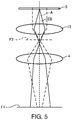
- FIG. 5 illustrates a state in which the focus of the imaging lens group 4 is shifted from the diffraction plane F2 of the objective lens 13.
- the diffraction plane F2 of the objective lens 13 is a back focal plane of the objective lens 13. On the diffraction plane F2 of the objective lens 13, an electron diffraction pattern is formed.
- a detection plane F4 is a plane in which the detection region 22 of the dark-field detector 20 is disposed.
- the diffraction plane F2 of the objective lens 13 and the detection plane F4 are conjugated.
- the electrons scattered by the specimen S at higher angles are converged stronger in the objective lens 13 as illustrated in FIG. 3 . Therefore, the electrons scattered by the specimen S in the range of from 50 mrad to 200 mrad cannot be accurately detected by the dark-field detector 20.
- the influence of the geometrical aberration on the electrons scattered by the specimen S in the range of from 50 mrad to 200 mrad is reduced by shifting the focus of the imaging lens group 4 from the diffraction plane F2 of the objective lens 13.
- the focus of the imaging lens group 4 is under-focused with respect to diffraction plane F2 by causing the excitation of the imaging lens group 4 to be weak.
- the difference in the focus position that depends on the angle generated by the geometrical aberration between the electrons scattered by the specimen S in the range of from 50 mrad to 200 mrad is corrected by defocus generated by shifting the focus of the imaging lens group 4 from the diffraction plane F2 of the objective lens 13.
- FIG. 6 illustrates State (a) in which the objective lens does not have a large geometrical aberration, and State (b) in which the objective lens has a large geometrical aberration.
- electron beams scattered at a low angle to a high angle are denoted by reference characters EB1, EB2, and EB3.
- the electrons scattered at high angles and the electrons scattered at low angles are converged at the same intensity. Therefore, as illustrated in State (a) in FIG. 6 , the electron beams EB2 and EB3 are detected by the dark-field detector 20 disposed in the detection plane F4.
- the electrons that are scattered at higher angles are converged stronger.
- the electron beam EB3 is detected by the dark-field detector 20 disposed in the detection plane F4.
- the detection results are different between the state in which the objective lens has a large geometrical aberration and the state in which the objective lens does not have a large geometrical aberration.
- a dark-field detector 20a disposed in a position closer to the specimen than the dark-field detector 20 disposed in the detection plane F4 and a dark-field detector 20b disposed in a position farther from the specimen than the dark-field detector 20 disposed in the detection plane F4 can detect the electron beams EB2 and EB3, and can obtain a detection result similar to that obtained in the state in which the objective lens does not have a large geometrical aberration.
- FIG. 7 illustrates a result obtained when the influence of the geometrical aberration on the electrons scattered by the specimen S in the range of from 50 mrad to 200 mrad is reduced.
- the electrons scattered by the specimen S in the range of from 50 mrad to 200 mrad can be accurately detected by the dark-field detector 20 by reducing the influence of the geometrical aberration on the electrons scattered by the specimen S in the range of from 50 mrad to 200 mrad.
- the imaging lens group 4 is under-focused with respect to the diffraction plane F2. Meanwhile, the imaging lens group 4 may be overfocused with respect to the diffraction plane F2 by causing the excitation of the imaging lens group 4 to be strong.
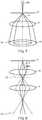
- FIG. 8 illustrates a state in which the focus of the imaging lens group 4 is shifted from the diffraction plane F2 of the objective lens 13.
- FIG. 8 illustrates a state in which the imaging lens group 4 is overfocused with respect to the diffraction plane F2.
- the imaging lens group 4 is overfocused with respect to the diffraction plane F2 by causing the excitation of the imaging lens group 4 to be strong.
- the electrons scattered by the specimen S in the range of from 50 mrad to 200 mrad can be accurately detected by the dark-field detector 20.
- the deviation of the electron beam EB from the optical axis A generated by shifting the focus of the imaging lens group 4 from the diffraction plane F2 is corrected with use of the de-scanning coil 18.
- the electron beam EB deflected from the optical axis A by shifting the focus of the imaging lens group 4 from the diffraction plane F2 is brought back to the optical axis A with use of the de-scanning coil 18. Therefore, the electron beam EB can be caused to match with the optical axis A.
- the electron beam EB can be prevented from moving in the detection plane F4 in accordance with the scanning with the electron beam EB.
- a method of acquiring a dark-field image according to one embodiment of the invention has the following effects, for example.
- a method of acquiring a dark-field image includes a step of reducing an influence of a geometrical aberration of electrons scattered in a predetermined angular range by shifting a focus of the imaging lens group 4 from the diffraction plane F2 of the objective lens 13. Therefore, even when the influence of the geometrical aberration of the objective lens 13 is large, the electrons scattered in a predetermined angular range can be accurately detected by the dark-field detector 20.
- the influence of the geometrical aberration is large, the electrons scattered at high angles have been needed to be cut by an aperture (not shown) disposed in an imaging system.
- the influence of the geometrical aberration on the electrons scattered in a predetermined angular range is reduced by shifting the focus of the imaging lens group 4 from the diffraction plane F2 of the objective lens 13, and hence a problem as above does not occur.
- a method of acquiring a dark-field image includes a step of correcting, with use of the de-scanning coil 18, a deviation of the electron beam EB from the optical axis A generated by shifting the focus of the imaging lens group 4 from the diffraction plane F2 of the objective lens 13. Therefore, the electron beam EB can be prevented from moving in the detection plane F4 in accordance with the scanning with the electron beam EB.
- the step of reducing the influence of the geometrical aberration includes correcting a difference in focus position that depends on an angle due to the geometrical aberration between the electrons scattered in the predetermined angular range by defocus generated by shifting the focus of the imaging lens group 4 from the diffraction plane F2 of the objective lens 13. Therefore, even when the influence of the geometrical aberration of the objective lens 13 is large, the electrons scattered in a predetermined angular range can be accurately detected by the dark-field detector 20.
- the dark-field detector 20 detects the electrons scattered by the specimen S in the range of from 50 mrad to 200 mrad.
- the range of the scattering angles that can be detected by the dark-field detector 20 is not particularly limited as long as the range is a range of high angles of 50 mrad or more.
- the invention includes configurations that are substantially the same (for example, in function and method) as the configurations described in the embodiments.
- the invention also includes configurations in which non-essential elements described in the embodiments are replaced by other elements.
- the invention further includes configurations obtained by adding known art to the configurations described in the embodiments.
Landscapes
- Chemical & Material Sciences (AREA)
- Analytical Chemistry (AREA)
- Analysing Materials By The Use Of Radiation (AREA)
Abstract
Description
- The present invention relates to a method of acquiring a dark-field image.
- A scanning transmission electron microscope (STEM) is an electron microscope that acquires a scanning transmission electron microscope image (STEM image) by scanning a converged electron beam over a specimen and mapping the intensity of detection signals obtained by transmitted electrons or scattered electrons from the specimen in synchronization with the scanning. In recent years, the scanning transmission electron microscope is attracting attention as an electron microscope with which an extremely high spatial resolution at the atomic scale can be obtained.
- In general, in a scanning electron microscope, when the STEM image is acquired, an imaging lens group formed by an intermediate lens and a projector lens is focused on a diffraction plane of an objective lens, and the diffraction plane of the objective lens and a detection plane of a detector are conjugated.
- As an observing technique using the scanning transmission electron microscope, high-angle annular dark-field scanning transmission electron microscopy (HAADF-STEM) is known (for example, see
JP-A-2009-152087 - In the high-angle annular dark-field scanning transmission electron microscopy, electrons scattered in a predetermined angular range can be detected by the annular detection region.
- When the geometrical aberration of the objective lens is large, the electrons scattered by the specimen are converged stronger as the angle by which the electrons are scattered is higher. Therefore, there may be cases where the electrons scattered in a predetermined angular range are not accurately detected even when the detector having the annular detection region is used.
- According to an aspect of the invention, there is provided a method of acquiring a dark-field image for a scanning transmission electron microscope,
the scanning transmission electron microscope including: - a dark-field detector having an annular detection region which is capable of detecting electrons scattered at a specimen in a predetermined angular range;
- an objective lens; and
- an imaging lens group disposed at a stage following the objective lens,
-
-
FIG. 1 illustrates a configuration of a scanning transmission electron microscope. -
FIG. 2 is a flowchart illustrating one example of a method of acquiring a dark-field image according to one embodiment of the invention. -
FIG. 3 illustrates a state in which an objective lens has a large geometrical aberration. -
FIG. 4 illustrates a state in which an imaging lens group is focused on a diffraction plane of an objective lens. -
FIG. 5 illustrates a state in which a focus of an imaging lens group is shifted from a diffraction plane of an objective lens. -
FIG. 6 illustrates State (a) in which an objective lens does not have a large geometrical aberration, and State (b) in which an objective lens has a large geometrical aberration. -
FIG. 7 illustrates a result obtained by reducing an influence of a geometrical aberration of electrons scattered by a specimen in a range of from 50 mrad to 200 mrad. -
FIG. 8 illustrates a state in which a focus of an imaging lens group is shifted from a diffraction plane of an objective lens. -
FIG. 9 illustrates a result obtained by reducing an influence of a geometrical aberration of electrons scattered by a specimen in a range of from 50 mrad to 200 mrad. - According to an embodiment of the invention, there is provided a method of acquiring a dark-field image for a scanning transmission electron microscope,
the scanning transmission electron microscope including: - a dark-field detector having an annular detection region which is capable of detecting electrons scattered at a specimen in a predetermined angular range;
- an objective lens; and
- an imaging lens group disposed at a stage following the objective lens,
- In the method of acquiring a dark-field image as above, even when the influence of the geometrical aberration of the objective lens is large, the electrons scattered in a predetermined angular range can be accurately detected by the dark-field detector.
- Preferred embodiments of the invention are described in detail below with reference to the drawings. It is noted that the following embodiments do not unduly limit the scope of the invention as stated in the claims. In addition, all of the elements described below are not necessarily essential requirements of the invention.
- First, a scanning transmission electron microscope used in a method of acquiring a dark-field image according to one embodiment of the invention is described with reference to the drawings.
FIG. 1 illustrates a configuration of a scanningtransmission electron microscope 100 used in the method of acquiring a dark-field image according to one embodiment of the invention. - As illustrated in
FIG. 1 , the scanningtransmission electron microscope 100 includes anelectron source 10, an illumination-lens system 11, ascanning deflector 12, anobjective lens 13, aspecimen stage 14, anintermediate lens 15, aprojector lens 16, a de-scanning coil 18 (one example of an imaging system deflector), and a dark-field detector 20. - The
electron source 10 generates an electron beam EB. Theelectron source 10 is an electron gun that emits the electron beam EB by accelerating electrons emitted from a cathode at an anode, for example. - The illumination-
lens system 11 converges the electron beam EB generated by theelectron source 10. Thescanning deflector 12 deflects the electron beam EB emitted from theelectron source 10. By supplying a scanning signal supplied from a control apparatus (not shown) to thescanning deflector 12, the converged electron beam EB can be scanned over a specimen S. - The
objective lens 13 converges the electron beam EB on the specimen S. By converging the electron beam EB by the illumination-lens system 11 and theobjective lens 13, an electron probe can be formed. Theobjective lens 13 images the electrons transmitted through the specimen S. - The
specimen stage 14 holds the specimen S. Thespecimen stage 14 can move the specimen S in the horizontal direction and the vertical direction and tilt the specimen S. - The
intermediate lens 15 is disposed in a stage following the objective lens 13 (the downstream side of the electron beam EB). Theprojector lens 16 is disposed in a stage following theintermediate lens 15. Theintermediate lens 15 and theprojector lens 16 form animaging lens group 4. Theimaging lens group 4 guides the electrons scattered by the specimen S at high angles to adetection region 22 of the dark-field detector 20. - The de-scanning
coil 18 is disposed between theobjective lens 13 and theintermediate lens 15. Thede-scanning coil 18 deflects the electron beam EB transmitted through the specimen S. - The dark-
field detector 20 is provided in a stage following theprojector lens 16. The dark-field detector 20 has theannular detection region 22. The dark-field detector 20 detects the electrons scattered by the specimen S in a predetermined angular range by thedetection region 22. For example, the dark-field detector 20 detects the electrons scattered by the specimen S in a range of from 50 mrad to 200 mrad. - Although not shown, the scanning
transmission electron microscope 100 may include a detector that detects electrons scattered by the specimen S at low angles and electrons transmitted through the specimen S without being scattered by the specimen S. - Next, a method of acquiring a dark-field image according to one embodiment of the invention is described.
FIG. 2 is a flowchart illustrating one example of the method of acquiring a dark-field image according to one embodiment of the invention. - The method of acquiring a dark-field image in the scanning
transmission electron microscope 100 includes a step (S10) of reducing the influence of the geometrical aberration on the electrons scattered in a predetermined angular range by shifting a focus of theimaging lens group 4 from the diffraction plane of theobjective lens 13. The method of acquiring a dark-field image in the scanningtransmission electron microscope 100 further includes a step (S20) of correcting, with use of thede-scanning coil 18, the deviation of the electron beam EB from an optical axis A generated by shifting the focus of theimaging lens group 4 from the diffraction plane of theobjective lens 13. - In the scanning
transmission electron microscope 100, the electrons scattered by the specimen S at high angles enter thedetection region 22 of the dark-field detector 20 by theobjective lens 13, theintermediate lens 15, and theprojector lens 16. The electrons scattered by the specimen S in the range of from 50 mrad to 200 mrad enter thedetection region 22 here. Therefore, the integrated intensities of the electrons scattered by the specimen S in the range of from 50 mrad to 200 mrad can be obtained. As a result, a HAADF-STEM image can be acquired in the scanningtransmission electron microscope 100. - The
objective lens 13 has geometrical aberrations such as the spherical aberration and the coma aberration. In particular, the spherical aberration has a great influence on the performance of the scanningtransmission electron microscope 100. -
FIG. 3 illustrates a state in which theobjective lens 13 has a large geometrical aberration. InFIG. 3 , theobjective lens 13, theintermediate lens 15, and theprojector lens 16 are expressed as oneimaging lens 2. - As illustrated in
FIG. 3 , when the geometrical aberration of theobjective lens 13 is large, the electrons that are scattered at higher angles are converged stronger in theobjective lens 13. As a result, the electrons scattered by the specimen S in the range of from 50 mrad to 200 mrad cannot be accurately detected by the dark-field detector 20. - In the scanning
transmission electron microscope 100, the influence of the geometrical aberration on the electrons scattered by the specimen S in the range of from 50 mrad to 200 mrad is reduced by shifting the focus of theimaging lens group 4 from the diffraction plane of theobjective lens 13. -
FIG. 4 illustrates a state in which theimaging lens group 4 is focused on a diffraction plane F2 of theobjective lens 13.FIG. 5 illustrates a state in which the focus of theimaging lens group 4 is shifted from the diffraction plane F2 of theobjective lens 13. - The diffraction plane F2 of the
objective lens 13 is a back focal plane of theobjective lens 13. On the diffraction plane F2 of theobjective lens 13, an electron diffraction pattern is formed. A detection plane F4 is a plane in which thedetection region 22 of the dark-field detector 20 is disposed. - As illustrated in
FIG. 4 , in a state in which theimaging lens group 4 is focused on the diffraction plane F2 of theobjective lens 13, the diffraction plane F2 of theobjective lens 13 and the detection plane F4 are conjugated. In this state, when the geometrical aberration of theobjective lens 13 is large, the electrons scattered by the specimen S at higher angles are converged stronger in theobjective lens 13 as illustrated inFIG. 3 . Therefore, the electrons scattered by the specimen S in the range of from 50 mrad to 200 mrad cannot be accurately detected by the dark-field detector 20. - Therefore, as illustrated in
FIG. 5 , the influence of the geometrical aberration on the electrons scattered by the specimen S in the range of from 50 mrad to 200 mrad is reduced by shifting the focus of theimaging lens group 4 from the diffraction plane F2 of theobjective lens 13. In the example illustrated inFIG. 5 , the focus of theimaging lens group 4 is under-focused with respect to diffraction plane F2 by causing the excitation of theimaging lens group 4 to be weak. - Specifically, the difference in the focus position that depends on the angle generated by the geometrical aberration between the electrons scattered by the specimen S in the range of from 50 mrad to 200 mrad is corrected by defocus generated by shifting the focus of the
imaging lens group 4 from the diffraction plane F2 of theobjective lens 13. -
FIG. 6 illustrates State (a) in which the objective lens does not have a large geometrical aberration, and State (b) in which the objective lens has a large geometrical aberration. InFIG. 6 , electron beams scattered at a low angle to a high angle are denoted by reference characters EB1, EB2, and EB3. - In the state in which the objective lens does not have a large geometrical aberration, the electrons scattered at high angles and the electrons scattered at low angles are converged at the same intensity. Therefore, as illustrated in State (a) in
FIG. 6 , the electron beams EB2 and EB3 are detected by the dark-field detector 20 disposed in the detection plane F4. - In the state in which the objective lens has a large geometrical aberration, the electrons that are scattered at higher angles are converged stronger. As illustrated in State (b) in
FIG. 6 , the electron beam EB3 is detected by the dark-field detector 20 disposed in the detection plane F4. As described above, the detection results are different between the state in which the objective lens has a large geometrical aberration and the state in which the objective lens does not have a large geometrical aberration. - As illustrated in State (b) in
FIG. 6 , even in the state in which the objective lens has a large geometrical aberration, a dark-field detector 20a disposed in a position closer to the specimen than the dark-field detector 20 disposed in the detection plane F4 and a dark-field detector 20b disposed in a position farther from the specimen than the dark-field detector 20 disposed in the detection plane F4 can detect the electron beams EB2 and EB3, and can obtain a detection result similar to that obtained in the state in which the objective lens does not have a large geometrical aberration. - Even when the dark-
field detector 20 disposed in the detection plane F4 is used, detection conditions equivalent to those in State (a) inFIG. 6 can be obtained by moving a plane conjugate to the detection plane F4 by shifting the focus of theimaging lens group 4 from the diffraction plane F2 of theobjective lens 13. In other words, the detection result similar to that obtained in the state in which the objective lens does not have a large geometrical aberration can be obtained. -
FIG. 7 illustrates a result obtained when the influence of the geometrical aberration on the electrons scattered by the specimen S in the range of from 50 mrad to 200 mrad is reduced. - As illustrated in
FIG. 7 , the electrons scattered by the specimen S in the range of from 50 mrad to 200 mrad can be accurately detected by the dark-field detector 20 by reducing the influence of the geometrical aberration on the electrons scattered by the specimen S in the range of from 50 mrad to 200 mrad. - As described above, in the example illustrated in
FIG. 5 , theimaging lens group 4 is under-focused with respect to the diffraction plane F2. Meanwhile, theimaging lens group 4 may be overfocused with respect to the diffraction plane F2 by causing the excitation of theimaging lens group 4 to be strong. -
FIG. 8 illustrates a state in which the focus of theimaging lens group 4 is shifted from the diffraction plane F2 of theobjective lens 13.FIG. 8 illustrates a state in which theimaging lens group 4 is overfocused with respect to the diffraction plane F2. - As illustrated in
FIG. 8 , theimaging lens group 4 is overfocused with respect to the diffraction plane F2 by causing the excitation of theimaging lens group 4 to be strong. As a result, as illustrated inFIG. 9 , the electrons scattered by the specimen S in the range of from 50 mrad to 200 mrad can be accurately detected by the dark-field detector 20. - As illustrated in
FIGS. 5 and8 , when the focus of theimaging lens group 4 is shifted from the diffraction plane F2 of theobjective lens 13, the diffraction plane F2 and the detection plane F4 are not conjugated. Therefore, when the electron beam EB is scanned over the specimen S, entering positions of the electrons in the detection plane F4 move in accordance with the scanning with the electron beam EB. - Therefore, in the scanning
transmission electron microscope 100, the deviation of the electron beam EB from the optical axis A generated by shifting the focus of theimaging lens group 4 from the diffraction plane F2 is corrected with use of thede-scanning coil 18. In other words, the electron beam EB deflected from the optical axis A by shifting the focus of theimaging lens group 4 from the diffraction plane F2 is brought back to the optical axis A with use of thede-scanning coil 18. Therefore, the electron beam EB can be caused to match with the optical axis A. As a result, the electron beam EB can be prevented from moving in the detection plane F4 in accordance with the scanning with the electron beam EB. - By shifting the focus of the
imaging lens group 4 from the diffraction plane F2, information of the image plane is included in the electron beam EB in the detection plane F4. However, the diameter of the electron beam EB is extremely small in the scanningtransmission electron microscope 100, and hence problems do not occur. - A method of acquiring a dark-field image according to one embodiment of the invention has the following effects, for example.
- A method of acquiring a dark-field image according to one embodiment of the invention includes a step of reducing an influence of a geometrical aberration of electrons scattered in a predetermined angular range by shifting a focus of the
imaging lens group 4 from the diffraction plane F2 of theobjective lens 13. Therefore, even when the influence of the geometrical aberration of theobjective lens 13 is large, the electrons scattered in a predetermined angular range can be accurately detected by the dark-field detector 20. - For example, when the influence of the geometrical aberration is large, the electrons scattered at high angles have been needed to be cut by an aperture (not shown) disposed in an imaging system. In a method of acquiring a dark-field image according to one embodiment of the invention, the influence of the geometrical aberration on the electrons scattered in a predetermined angular range is reduced by shifting the focus of the
imaging lens group 4 from the diffraction plane F2 of theobjective lens 13, and hence a problem as above does not occur. - A method of acquiring a dark-field image according to one embodiment of the invention includes a step of correcting, with use of the
de-scanning coil 18, a deviation of the electron beam EB from the optical axis A generated by shifting the focus of theimaging lens group 4 from the diffraction plane F2 of theobjective lens 13. Therefore, the electron beam EB can be prevented from moving in the detection plane F4 in accordance with the scanning with the electron beam EB. - In a method of acquiring a dark-field image according to one embodiment of the invention, the step of reducing the influence of the geometrical aberration includes correcting a difference in focus position that depends on an angle due to the geometrical aberration between the electrons scattered in the predetermined angular range by defocus generated by shifting the focus of the
imaging lens group 4 from the diffraction plane F2 of theobjective lens 13. Therefore, even when the influence of the geometrical aberration of theobjective lens 13 is large, the electrons scattered in a predetermined angular range can be accurately detected by the dark-field detector 20. - The invention is not limited to the abovementioned embodiments and may be modified and embodied in various ways within the scope of the invention.
- For example, in the abovementioned embodiments, a case where the dark-
field detector 20 detects the electrons scattered by the specimen S in the range of from 50 mrad to 200 mrad has been described. However, the range of the scattering angles that can be detected by the dark-field detector 20 is not particularly limited as long as the range is a range of high angles of 50 mrad or more. - The invention includes configurations that are substantially the same (for example, in function and method) as the configurations described in the embodiments. The invention also includes configurations in which non-essential elements described in the embodiments are replaced by other elements. The invention further includes configurations obtained by adding known art to the configurations described in the embodiments.
- Some embodiments of the invention have been described in detail above, but a person skilled in the art will readily appreciate that various modifications can be made from the embodiments without materially departing from the novel teachings and effects of the invention, as defined by the claims. Accordingly, all such modifications are assumed to be included in the scope of the invention.
reducing an influence of a geometrical aberration on the electrons scattered in the predetermined angular range by shifting a focus of the imaging lens group from a diffraction plane of the objective lens.
reducing an influence of a geometrical aberration on the electrons scattered in the predetermined angular range by shifting a focus of the imaging lens group from a diffraction plane of the objective lens.
Claims (5)
- A method of acquiring a dark-field image for a scanning transmission electron microscope,
the scanning transmission electron microscope comprising:a dark-field detector having an annular detection region which is capable of detecting electrons scattered at a specimen in a predetermined angular range;an objective lens; andan imaging lens group disposed at a stage following the objective lens,the method comprising:
reducing an influence of a geometrical aberration on the electrons scattered in the predetermined angular range by shifting a focus of the imaging lens group from a diffraction plane of the objective lens. - The method of acquiring a dark-field image according to claim 1, wherein
the scanning transmission electron microscope includes an imaging system deflector that deflects an electron beam transmitted through the specimen, and
the method further comprises correcting, with use of the imaging system deflector, a deviation of the electron beam from an optical axis generated by shifting the focus of the imaging lens group from the diffraction plane of the objective lens. - The method of acquiring a dark-field image according to claim 1 or 2, wherein
the imaging lens group includes an intermediate lens and a projector lens that are disposed at a stage following the objective lens. - The method of acquiring a dark-field image according to any one of claims 1 to 3, wherein
the predetermined angular range is from 50 mrad to 200 mrad. - The method of acquiring a dark-field image according to any one of claims 1 to 4, wherein
reducing the influence of the geometrical aberration includes correcting a difference in focus position that depends on an angle generated by the geometrical aberration between the electrons scattered in the predetermined angular range by defocus generated by shifting the focus of the imaging lens group from the diffraction plane of the objective lens.
Applications Claiming Priority (1)
| Application Number | Priority Date | Filing Date | Title |
|---|---|---|---|
| JP2019166010A JP6962979B2 (en) | 2019-09-12 | 2019-09-12 | How to get a darkfield image |
Publications (1)
| Publication Number | Publication Date |
|---|---|
| EP3792954A1 true EP3792954A1 (en) | 2021-03-17 |
Family
ID=72474136
Family Applications (1)
| Application Number | Title | Priority Date | Filing Date |
|---|---|---|---|
| EP20195802.2A Pending EP3792954A1 (en) | 2019-09-12 | 2020-09-11 | Method of acquiring dark-field image |
Country Status (3)
| Country | Link |
|---|---|
| US (1) | US11462384B2 (en) |
| EP (1) | EP3792954A1 (en) |
| JP (1) | JP6962979B2 (en) |
Families Citing this family (1)
| Publication number | Priority date | Publication date | Assignee | Title |
|---|---|---|---|---|
| JP7693426B2 (en) * | 2021-07-12 | 2025-06-17 | キオクシア株式会社 | Analysis method |
Citations (6)
| Publication number | Priority date | Publication date | Assignee | Title |
|---|---|---|---|---|
| JP2007180013A (en) * | 2005-11-30 | 2007-07-12 | Jeol Ltd | Aberration measurement method, aberration correction method and electron microscope using Ronchigram |
| JP2009152087A (en) | 2007-12-21 | 2009-07-09 | Jeol Ltd | Transmission electron microscope |
| JP2012022971A (en) * | 2010-07-16 | 2012-02-02 | Univ Of Tokyo | Aberration correction method and aberration correction device for scanning transmission electron microscope |
| JP2012043563A (en) * | 2010-08-16 | 2012-03-01 | Fujitsu Ltd | Confocal scanning transmission type electron microscope device and three-dimensional tomographic observation method |
| EP2592641A1 (en) * | 2010-07-05 | 2013-05-15 | Hitachi High-Technologies Corporation | Scanning transmission type electron microscope |
| US20170236684A1 (en) * | 2016-02-03 | 2017-08-17 | Jeol Ltd. | Electron Microscope and Method of Aberration Measurement |
Family Cites Families (12)
| Publication number | Priority date | Publication date | Assignee | Title |
|---|---|---|---|---|
| WO1998038669A1 (en) * | 1997-02-28 | 1998-09-03 | Arizona Board Of Regents | Atomic focusers in electron microscopy |
| JP2005032732A (en) * | 2004-09-15 | 2005-02-03 | Hitachi Ltd | Scanning electron microscope |
| EP1796130A1 (en) * | 2005-12-06 | 2007-06-13 | FEI Company | Method for determining the aberration coefficients of the aberration function of a particle-optical lens. |
| JP2007179753A (en) * | 2005-12-27 | 2007-07-12 | Hitachi High-Technologies Corp | Scanning transmission electron microscope and aberration measurement method |
| JP5188846B2 (en) * | 2008-03-10 | 2013-04-24 | 日本電子株式会社 | Aberration correction apparatus and aberration correction method for scanning transmission electron microscope |
| JP5871440B2 (en) * | 2010-07-14 | 2016-03-01 | エフ・イ−・アイ・カンパニー | Contrast improvement of scanning confocal electron microscope |
| JP5735262B2 (en) * | 2010-11-12 | 2015-06-17 | 株式会社日立ハイテクノロジーズ | Charged particle optical apparatus and lens aberration measuring method |
| JP5712074B2 (en) * | 2011-07-20 | 2015-05-07 | 株式会社日立ハイテクノロジーズ | Scanning transmission electron microscope |
| US8598527B2 (en) * | 2011-11-22 | 2013-12-03 | Mochii, Inc. | Scanning transmission electron microscopy |
| JP5934513B2 (en) * | 2012-02-09 | 2016-06-15 | 日本電子株式会社 | Transmission electron microscope |
| JP6163063B2 (en) * | 2013-09-13 | 2017-07-12 | 株式会社日立ハイテクノロジーズ | Scanning transmission electron microscope and aberration measurement method thereof |
| EP3379236B1 (en) * | 2017-03-20 | 2019-09-11 | TESCAN Brno, s.r.o. | Scanning transmission electron microscope |
-
2019
- 2019-09-12 JP JP2019166010A patent/JP6962979B2/en active Active
-
2020
- 2020-09-11 US US17/017,840 patent/US11462384B2/en active Active
- 2020-09-11 EP EP20195802.2A patent/EP3792954A1/en active Pending
Patent Citations (6)
| Publication number | Priority date | Publication date | Assignee | Title |
|---|---|---|---|---|
| JP2007180013A (en) * | 2005-11-30 | 2007-07-12 | Jeol Ltd | Aberration measurement method, aberration correction method and electron microscope using Ronchigram |
| JP2009152087A (en) | 2007-12-21 | 2009-07-09 | Jeol Ltd | Transmission electron microscope |
| EP2592641A1 (en) * | 2010-07-05 | 2013-05-15 | Hitachi High-Technologies Corporation | Scanning transmission type electron microscope |
| JP2012022971A (en) * | 2010-07-16 | 2012-02-02 | Univ Of Tokyo | Aberration correction method and aberration correction device for scanning transmission electron microscope |
| JP2012043563A (en) * | 2010-08-16 | 2012-03-01 | Fujitsu Ltd | Confocal scanning transmission type electron microscope device and three-dimensional tomographic observation method |
| US20170236684A1 (en) * | 2016-02-03 | 2017-08-17 | Jeol Ltd. | Electron Microscope and Method of Aberration Measurement |
Also Published As
| Publication number | Publication date |
|---|---|
| JP6962979B2 (en) | 2021-11-05 |
| JP2021044175A (en) | 2021-03-18 |
| US11462384B2 (en) | 2022-10-04 |
| US20210082663A1 (en) | 2021-03-18 |
Similar Documents
| Publication | Publication Date | Title |
|---|---|---|
| US8153969B2 (en) | Inspection method and inspection system using charged particle beam | |
| JP6278553B2 (en) | Secondary electron optical system and detection device | |
| US20070158567A1 (en) | Apparatus and adjusting method for a scanning transmission electron microscope | |
| CN113466266B (en) | Method and system for acquiring 3D diffraction data | |
| WO2012063749A1 (en) | Charged particle optical equipment and method for measuring lens aberration | |
| JP2017139115A (en) | Electron microscope and aberration measurement method | |
| US10971328B2 (en) | Charged particle beam device | |
| US10923314B2 (en) | Method of image acquisition and electron microscope | |
| US20190006145A1 (en) | Method of verifying operation parameter of scanning electron microscope | |
| CN113125478A (en) | Method and system for automatic alignment of ribbon axes | |
| US5747814A (en) | Method for centering a lens in a charged-particle system | |
| US11462384B2 (en) | Method of acquiring dark-field image | |
| US11791131B2 (en) | Charged particle beam apparatus and method for controlling charged particle beam apparatus | |
| US8710438B2 (en) | Scanning transmission electron microscope and axial adjustment method thereof | |
| US8124940B2 (en) | Charged particle beam apparatus | |
| WO2025004191A1 (en) | Charged particle beam device | |
| US11251016B2 (en) | Method of controlling transmission electron microscope and transmission electron microscope | |
| JP7498212B2 (en) | Electron microscope and aberration measurement method | |
| US12518944B2 (en) | Electron microscope and image acquisition method | |
| JP2021176143A (en) | Scanning transmission electron microscope and adjustment method of optical system | |
| US20250354945A1 (en) | Image Acquisition Method and Scanning Transmission Electron Microscope | |
| US11456151B2 (en) | Image acquisition method and electron microscope |
Legal Events
| Date | Code | Title | Description |
|---|---|---|---|
| PUAI | Public reference made under article 153(3) epc to a published international application that has entered the european phase |
Free format text: ORIGINAL CODE: 0009012 |
|
| STAA | Information on the status of an ep patent application or granted ep patent |
Free format text: STATUS: THE APPLICATION HAS BEEN PUBLISHED |
|
| AK | Designated contracting states |
Kind code of ref document: A1 Designated state(s): AL AT BE BG CH CY CZ DE DK EE ES FI FR GB GR HR HU IE IS IT LI LT LU LV MC MK MT NL NO PL PT RO RS SE SI SK SM TR |
|
| AX | Request for extension of the european patent |
Extension state: BA ME |
|
| STAA | Information on the status of an ep patent application or granted ep patent |
Free format text: STATUS: REQUEST FOR EXAMINATION WAS MADE |
|
| 17P | Request for examination filed |
Effective date: 20210901 |
|
| RBV | Designated contracting states (corrected) |
Designated state(s): AL AT BE BG CH CY CZ DE DK EE ES FI FR GB GR HR HU IE IS IT LI LT LU LV MC MK MT NL NO PL PT RO RS SE SI SK SM TR |