EP3792907A1 - Display panel and terminal device - Google Patents
Display panel and terminal device Download PDFInfo
- Publication number
- EP3792907A1 EP3792907A1 EP20171848.3A EP20171848A EP3792907A1 EP 3792907 A1 EP3792907 A1 EP 3792907A1 EP 20171848 A EP20171848 A EP 20171848A EP 3792907 A1 EP3792907 A1 EP 3792907A1
- Authority
- EP
- European Patent Office
- Prior art keywords
- display panel
- light
- light transmitting
- layer
- hole
- Prior art date
- Legal status (The legal status is an assumption and is not a legal conclusion. Google has not performed a legal analysis and makes no representation as to the accuracy of the status listed.)
- Pending
Links
Images


Classifications
-
- H—ELECTRICITY
- H10—SEMICONDUCTOR DEVICES; ELECTRIC SOLID-STATE DEVICES NOT OTHERWISE PROVIDED FOR
- H10K—ORGANIC ELECTRIC SOLID-STATE DEVICES
- H10K59/00—Integrated devices, or assemblies of multiple devices, comprising at least one organic light-emitting element covered by group H10K50/00
- H10K59/30—Devices specially adapted for multicolour light emission
- H10K59/35—Devices specially adapted for multicolour light emission comprising red-green-blue [RGB] subpixels
-
- H—ELECTRICITY
- H10—SEMICONDUCTOR DEVICES; ELECTRIC SOLID-STATE DEVICES NOT OTHERWISE PROVIDED FOR
- H10K—ORGANIC ELECTRIC SOLID-STATE DEVICES
- H10K59/00—Integrated devices, or assemblies of multiple devices, comprising at least one organic light-emitting element covered by group H10K50/00
- H10K59/10—OLED displays
- H10K59/12—Active-matrix OLED [AMOLED] displays
- H10K59/122—Pixel-defining structures or layers, e.g. banks
-
- G—PHYSICS
- G09—EDUCATION; CRYPTOGRAPHY; DISPLAY; ADVERTISING; SEALS
- G09G—ARRANGEMENTS OR CIRCUITS FOR CONTROL OF INDICATING DEVICES USING STATIC MEANS TO PRESENT VARIABLE INFORMATION
- G09G3/00—Control arrangements or circuits, of interest only in connection with visual indicators other than cathode-ray tubes
- G09G3/20—Control arrangements or circuits, of interest only in connection with visual indicators other than cathode-ray tubes for presentation of an assembly of a number of characters, e.g. a page, by composing the assembly by combination of individual elements arranged in a matrix no fixed position being assigned to or needed to be assigned to the individual characters or partial characters
- G09G3/22—Control arrangements or circuits, of interest only in connection with visual indicators other than cathode-ray tubes for presentation of an assembly of a number of characters, e.g. a page, by composing the assembly by combination of individual elements arranged in a matrix no fixed position being assigned to or needed to be assigned to the individual characters or partial characters using controlled light sources
- G09G3/30—Control arrangements or circuits, of interest only in connection with visual indicators other than cathode-ray tubes for presentation of an assembly of a number of characters, e.g. a page, by composing the assembly by combination of individual elements arranged in a matrix no fixed position being assigned to or needed to be assigned to the individual characters or partial characters using controlled light sources using electroluminescent panels
- G09G3/32—Control arrangements or circuits, of interest only in connection with visual indicators other than cathode-ray tubes for presentation of an assembly of a number of characters, e.g. a page, by composing the assembly by combination of individual elements arranged in a matrix no fixed position being assigned to or needed to be assigned to the individual characters or partial characters using controlled light sources using electroluminescent panels semiconductive, e.g. using light-emitting diodes [LED]
- G09G3/3208—Control arrangements or circuits, of interest only in connection with visual indicators other than cathode-ray tubes for presentation of an assembly of a number of characters, e.g. a page, by composing the assembly by combination of individual elements arranged in a matrix no fixed position being assigned to or needed to be assigned to the individual characters or partial characters using controlled light sources using electroluminescent panels semiconductive, e.g. using light-emitting diodes [LED] organic, e.g. using organic light-emitting diodes [OLED]
-
- H—ELECTRICITY
- H04—ELECTRIC COMMUNICATION TECHNIQUE
- H04M—TELEPHONIC COMMUNICATION
- H04M1/00—Substation equipment, e.g. for use by subscribers
- H04M1/02—Constructional features of telephone sets
- H04M1/0202—Portable telephone sets, e.g. cordless phones, mobile phones or bar type handsets
- H04M1/026—Details of the structure or mounting of specific components
- H04M1/0264—Details of the structure or mounting of specific components for a camera module assembly
-
- H—ELECTRICITY
- H10—SEMICONDUCTOR DEVICES; ELECTRIC SOLID-STATE DEVICES NOT OTHERWISE PROVIDED FOR
- H10K—ORGANIC ELECTRIC SOLID-STATE DEVICES
- H10K50/00—Organic light-emitting devices
- H10K50/10—OLEDs or polymer light-emitting diodes [PLED]
- H10K50/14—Carrier transporting layers
- H10K50/15—Hole transporting layers
-
- H—ELECTRICITY
- H10—SEMICONDUCTOR DEVICES; ELECTRIC SOLID-STATE DEVICES NOT OTHERWISE PROVIDED FOR
- H10K—ORGANIC ELECTRIC SOLID-STATE DEVICES
- H10K50/00—Organic light-emitting devices
- H10K50/10—OLEDs or polymer light-emitting diodes [PLED]
- H10K50/14—Carrier transporting layers
- H10K50/16—Electron transporting layers
-
- H—ELECTRICITY
- H10—SEMICONDUCTOR DEVICES; ELECTRIC SOLID-STATE DEVICES NOT OTHERWISE PROVIDED FOR
- H10K—ORGANIC ELECTRIC SOLID-STATE DEVICES
- H10K59/00—Integrated devices, or assemblies of multiple devices, comprising at least one organic light-emitting element covered by group H10K50/00
- H10K59/10—OLED displays
- H10K59/17—Passive-matrix OLED displays
- H10K59/173—Passive-matrix OLED displays comprising banks or shadow masks
-
- H—ELECTRICITY
- H10—SEMICONDUCTOR DEVICES; ELECTRIC SOLID-STATE DEVICES NOT OTHERWISE PROVIDED FOR
- H10K—ORGANIC ELECTRIC SOLID-STATE DEVICES
- H10K59/00—Integrated devices, or assemblies of multiple devices, comprising at least one organic light-emitting element covered by group H10K50/00
- H10K59/60—OLEDs integrated with inorganic light-sensitive elements, e.g. with inorganic solar cells or inorganic photodiodes
-
- H—ELECTRICITY
- H10—SEMICONDUCTOR DEVICES; ELECTRIC SOLID-STATE DEVICES NOT OTHERWISE PROVIDED FOR
- H10K—ORGANIC ELECTRIC SOLID-STATE DEVICES
- H10K59/00—Integrated devices, or assemblies of multiple devices, comprising at least one organic light-emitting element covered by group H10K50/00
- H10K59/80—Constructional details
- H10K59/87—Passivation; Containers; Encapsulations
- H10K59/873—Encapsulations
-
- H—ELECTRICITY
- H10—SEMICONDUCTOR DEVICES; ELECTRIC SOLID-STATE DEVICES NOT OTHERWISE PROVIDED FOR
- H10K—ORGANIC ELECTRIC SOLID-STATE DEVICES
- H10K59/00—Integrated devices, or assemblies of multiple devices, comprising at least one organic light-emitting element covered by group H10K50/00
- H10K59/80—Constructional details
- H10K59/8791—Arrangements for improving contrast, e.g. preventing reflection of ambient light
- H10K59/8792—Arrangements for improving contrast, e.g. preventing reflection of ambient light comprising light absorbing layers, e.g. black layers
-
- G—PHYSICS
- G09—EDUCATION; CRYPTOGRAPHY; DISPLAY; ADVERTISING; SEALS
- G09G—ARRANGEMENTS OR CIRCUITS FOR CONTROL OF INDICATING DEVICES USING STATIC MEANS TO PRESENT VARIABLE INFORMATION
- G09G2360/00—Aspects of the architecture of display systems
- G09G2360/14—Detecting light within display terminals, e.g. using a single or a plurality of photosensors
- G09G2360/145—Detecting light within display terminals, e.g. using a single or a plurality of photosensors the light originating from the display screen
-
- H—ELECTRICITY
- H10—SEMICONDUCTOR DEVICES; ELECTRIC SOLID-STATE DEVICES NOT OTHERWISE PROVIDED FOR
- H10K—ORGANIC ELECTRIC SOLID-STATE DEVICES
- H10K59/00—Integrated devices, or assemblies of multiple devices, comprising at least one organic light-emitting element covered by group H10K50/00
- H10K59/60—OLEDs integrated with inorganic light-sensitive elements, e.g. with inorganic solar cells or inorganic photodiodes
- H10K59/65—OLEDs integrated with inorganic image sensors
Definitions
- the present disclosure relates to the field of electronic devices, and in particular to a display panel and a terminal device.
- the present disclosure provides a display panel and a terminal device in accordance with claims as follows.
- a display panel having a display area.
- the display area includes a photosensitive area, a plurality of pixel units are arranged in an array in the photosensitive area, and a light transmitting hole is provided between adjacent pixel units in the photosensitive area.
- the photosensitive area is provided in the display area, and the light transmitting hole is provided between adjacent pixel units in the photosensitive area.
- a photosensitive element such as a camera module and a fingerprint module of a terminal device may be disposed under the display device, and the photosensitive element realizes optical signal transmission through a plurality of the light transmitting holes in the display panel. Because the size of the light transmitting hole is small, based on the principle of pin-hole imaging, each hole may pass through external light in a large range, and corresponding function thereof can be implemented.
- the photosensitive element is disposed under the display panel instead of being disposed on a front side of the display panel, so the full-screen design can be implemented and the appearance of the device can be improved.
- the light transmitting hole penetrates through a non-transparent film layer in the display panel.
- the light transmitting hole is formed only in the non-transparent film layer, which can reduce workload of forming the hole on the one hand, and ensure the overall strength of the panel on the other hand.
- the display panel is an OLED display panel.
- the OLED display panel includes a pixel defining layer a cathode layer, an electron transport layer, and an organic light emitting layer, a hole transport layer, an anode layer and a protective layer which are stacked, and the light transmitting hole penetrates through the pixel defining layer and the hole transport layer.
- each of the cathode layer, electron transport layer and organic light emitting layer is not formed integrally and is disposed only in a sub-pixel area, and each of the anode layer and the protective layer is formed integrally and is a transparent film layer, the light emitting hole needs only to penetrate through the pixel defining layer and the hole transport layer.
- a light shielding layer is disposed on an inner side surface of the display panel, a vial hole is disposed in the light shielding layer to correspond to the light transmitting hole, and the inner side surface and a light-exiting surface of the display panel are two opposite surfaces of the display panel.
- the light shielding layer is disposed on the inner side surface of the display panel to shield light generated by the display panel to prevent the same from reaching the photosensitive element and thus affecting a normal operation of the photosensitive element. At the same time, the light shielding layer does not shield the light transmitting hole, so that external light may still pass through the light transmitting hole, which can ensure the normal operation of the photosensitive element.
- a light shielding film is disposed on a side wall of the light transmitting hole.
- the light shielding film is coated on the side wall of the light transmitting hole, which can further prevent the light generated by the display panel from affecting the photosensitive element.
- a strip-shaped area is located between the adjacent pixel units, and a plurality of the light transmitting holes are spaced apart in a longitudinal direction of the strip-shaped area.
- the plurality of light transmitting holes are arranged in the strip-shaped area between the adjacent pixel units, which can ensure light transmitting area in the photosensitive area, and thus can ensure that the photosensitive element can be operated normally through these light transmitting holes.
- the photosensitive element may obtain light from all parts in an external environment without dead parts. In this case, when a camera module is used, a whole image of the external environment can be obtained.
- the light transmitting hole is a circular hole with a diameter being 1/3 ⁇ 2/3 of a minimum width of the strip-shaped area.
- the diameter of the light transmitting hole is defined to be 1/3 ⁇ 2/3 of the minimum width of the strip-shaped area, on the one hand, the size of the hole is prevented from being too large to affect normal arrangement of the pixels units, and on the other hand, the area of the hole can ensure the normal operation of the photosensitive element.
- a distance between adjacent light transmitting holes is 50% ⁇ 100% of the diameter of the light transmitting hole.
- the light transmitting holes are spaced apart, and the distance between the light transmitting holes is defined to be 50% ⁇ 100% of the diameter of the light transmitting hole, on the one hand, it can prevent the holes from being to connected to each other to make the hole too large to be observed by eyes, on the other hand, the distance between the holes is prevented from being too large to affect the number of the holes, and thus can ensure light transmitting area, and on the further other hand, light can be obtained from all parts in the external environment without dead parts by pin-hole imaging.
- a terminal device including: the display panel according to any one of the above embodiments; and a photosensitive element, disposed on a first side of the display pane, wherein the first side is a side facing away from a light-exiting surface of the display panel, and the photosensitive element is arranged is in the photosensitive area of the display panel.
- the terminal device further includes: a processing unit configured to perform filtering processing on an electrical signal generated by the photosensitive element.
- the processing unit is employed to perform the filtering processing on the electrical signal of the photosensitive element, so that the noise of the electrical signal of the photosensitive element is reduced and thus the electrical signal has a high accuracy.
- the processing unit is configured to perform differential processing on the electrical signal generated by the photosensitive element and a preset signal, and the preset signal is an electrical signal when the photosensitive element receives only light generated by the display panel.
- the processing unit may filter signal through differential processing.
- the processing unit may first obtain and store the electrical signal only when the light is only generated by the display panel as the preset signal. When performing the processing, the preset signal is subtracted from the electrical signal to filter the signal.
- the photosensitive element includes at least one of a camera module, an optical sensor, and an optical fingerprint module.
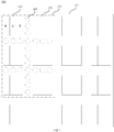
- FIG. 1 is a schematic structural diagram of a display panel according to an embodiment of the present disclosure.
- the display panel 100 has a display area 101 including a photosensitive area 102.
- a plurality of pixel units 110 are arranged in an array in the photosensitive area 102.
- a light transmitting hole 103 is provided between adjacent pixel units 110 in the photosensitive area 102.
- the light transmitting hole 103 is an optical micro-hole with a micron order. On the one hand, the light transmitting is guaranteed, and on the other hand, human eyes cannot see the light transmitting hole, which does not affect the appearance of the display panel.
- the photosensitive area is provided in the display area, and the light transmitting hole is provided between adjacent pixel units in the photosensitive area.
- a photosensitive element such as a camera module and a fingerprint module of a terminal device may be disposed under the display device, and the photosensitive element realizes optical signal transmission through a plurality of the light-transmitting holes in the display panel. Because the size of the light transmitting hole is small, based on the principle of pin-hole imaging, through each hole may pass external light in a large range, and corresponding function thereof can be implemented.
- the photosensitive element is disposed under the display panel instead of being disposed on a front side of the display panel, so the full-screen design can be implemented and the appearance of the device can be improved.
- the display panel 100 may be an organic light emitting diode (OLED) display panel.
- OLED organic light emitting diode
- a high resolution of the OLED display panel makes the distribution of the light transmitting holes more uniform, thereby ensuring the normal operation of the photosensitive element.
- the display panel 100 may also be other display panels, such as a micro LED display panel, a quantum dot light emitting diode (QLED) display panel, and the like.
- QLED quantum dot light emitting diode
- each pixel unit 110 may include a plurality of sub-pixel units.
- the pixel unit 110 includes three sub-pixel units of red (R), green (G), and blue (B).
- FIG. 2 is a partially enlarged view of a display panel according to an embodiment of the present disclosure.
- a strip-shaped area 111 between adjacent pixel units 110, and a plurality of light transmitting holes 103 are spaced apart or arranged at intervals along a longitudinal direction of the strip-shaped area 111.
- the plurality of light transmitting holes are arranged in the strip-shaped area between the adjacent pixel units, which can ensure light transmitting area in the photosensitive area, and thus can ensure that the photosensitive element can operate normally through these light transmitting holes.
- the photosensitive element may obtain light from all parts in an external environment without dead parts. In this case, when a camera module is used, a whole image of the external environment can be obtained.
- the shapes of the three sub-pixel units R, G, and B may be rectangular (there is also a distance between the sub-pixel units, which is not shown in FIGs. 1 and 2 ).
- the pixel unit is also a rectangle, and the stripe-shaped area 111 between the pixel units is a rectangular area.
- the longitudinal direction of the stripe-shaped area 111 is the column direction A.
- the shapes of the sub-pixel unit and the pixel unit may be of any other shape.
- the stripe-shaped area 111 between the pixel units may be another regular or irregular-shaped area.
- the respective sub-pixel units in the same pixel unit are arranged in a row direction. In another embodiment, the respective sub-pixel units in the same pixel unit may also be arranged in a column direction or in an irregular manner.
- the light transmitting hole 103 may be a circle hole, which is easy to be designed and manufactured.
- the diameter of the light transmitting hole 103 may be 1/3 to 2/3 of a minimum width d of the strip-shaped area 111.
- the diameter of the light transmitting hole is defined to be 1/3 ⁇ 2/3 of the minimum width of the strip-shaped area, on the one hand, the size of the hole is prevented from being too large to affect normal arrangement of the pixels units, and on the other hand, the area of the hole can ensure the normal operation of the photosensitive element.
- the diameter of the light transmitting hole 103 may be 1/2 of the minimum width d of the strip-shaped area 111.
- the light transmitting hole 103 may have other shapes, such as a rectangle, which is not limited in the present disclosure.
- a distance s between the adjacent light transmitting holes 103 may be 50% to 100% of the diameter of the light transmitting hole 103.
- the light transmitting holes are spaced apart, and the distance between the light transmitting holes is defined to be 50% ⁇ 100% of the diameter of the light-transmitting hole, on the one hand, it can prevent the holes from being to close to each other to make the hole too large to be observed by human eyes, on the other hand, the distance between the holes is prevented from being too large to affect the number of the holes, and thus can ensure a light transmitting area, and on the further other hand, light can be obtained from all parts in the external environment without dead parts by pin-hole imaging.
- the distance s between the adjacent light transmitting holes 103 may be 50% of the diameter of the light transmitting hole 103.
- FIG. 3 is a schematic structural diagram of a display panel according to an embodiment of the present disclosure.
- a light shielding layer 120 is provided on an inner side surface of the display panel 100, and a via hole 121 is provided in the light shielding layer 120 to correspond to the light transmitting hole 103.
- the inner side surface and a light exiting surface of the display panel 100 are two opposite surfaces of the display panel.
- the light shielding layer is disposed on the inner side surface of the display panel to shield light generated by the display panel to prevent the same from reaching the photosensitive element and thus affecting a normal operation of the photosensitive element. At the same time, the light shielding layer does not shield the light transmitting hole, so that external light signal may still pass through the light transmitting hole, which can ensure the normal operation of the photosensitive element.
- the "correspond to” herein may refer to that the projection of the light transmitting hole 103 on the light-exiting surface is overlapped with the projection of the via hole 121 on the light-exiting surface, so as to ensure that the light passing through the light transmitting hole will not be blocked.
- the light shielding layer 120 may be made of a metal layer or other light-shielding ink (for example, a black ink).
- the film layer of the display panel may be directly formed on the metal layer.
- the light-shielding ink may be applied on the display panel after the display panel is manufactured.
- a light shielding film 130 is disposed on a sidewall of the light transmitting hole 103.
- the light shielding film is coated on the side wall of the light transmitting hole, which can further prevent the light generated by the display panel from affecting the photosensitive element.
- the light-shielding film 130 may be a light-shielding ink film.
- the light-shielding ink film 130 may be fabricated on the sidewall of the light transmitting hole 103 by spray coating, printing, evaporation, or other methods.
- FIG. 4 is a schematic diagram of a layer stack of a display panel according to an embodiment of the present disclosure.
- the display panel 100 includes a pixel defining layer 141, a cathode layer 142, an electron transport layer 143, an organic light emitting layer 144, a hole transport layer 145, an anode layer 146, and a protective layer 147, which are stacked.
- the pixel defining layer 141 is used to define a plurality of grooves, and each groove corresponds to a sub-pixel unit.
- the cathode layer 142, the electron transport layer 143, and the organic light emitting layer 144 are all grown in the groove, that is, these layers each include a plurality of parts, and each part corresponds to a sub-pixel unit.
- the cathode layer, electron transport layer, and organic light emitting layer of each sub-pixel are formed in the groove.
- the hole transport layer 145, the anode layer 146, and the protective layer 147 are designed on the entire surface, and do not need to be divided according to the sub-pixel units.
- the electron transport layer 143, the organic light emitting layer 144, and the hole transport layer 145 can all be formed by printing or evaporation of an organic material.
- the cathode layer 142 may be a metal cathode, and the anode layer 146 may be an indium tin oxide (ITO) anode.
- the protective layer 147 may be a glass plate.
- the cathode layer 142 is a metal cathode, and has a light-shielding property, since there is no cathode in the area between the sub-pixels, the light of the display panel will still pass through, so the aforementioned light-shielding layer 120 needs to be provided for shielding.
- the light transmitting holes 103 are formed between the pixel units, in fact, the light transmitting holes 103 only need to penetrate through the pixel defining layer 141, the hole transport layer 145, the anode layer 146, and the protective layer 147.
- the protective layer 147 is a glass plate, and the anode layer 146 is an ITO layer, both of which are transparent, so the light transmitting hole 103 only needs to penetrate through the pixel defining layer 141 and the hole transport layer 145.
- the light transmitting hole 103 penetrates through a non-transparent film layer in the display panel.
- the light transmitting hole is formed only in the non-transparent film layer, which can reduce workload of forming the hole on the one hand, and ensure the overall strength of the panel on the other hand.
- the light shielding layer 120 is disposed on the bottom surface (the side facing away from the light exiting surface) of the pixel defining layer 141 of the display panel 100.
- FIG. 4 provides a schematic structural diagram of a passive-driving (PM) OLED display panel.
- the OLED display panel is an active-driving (AM) OLED display panel
- the display panel further includes a thin film transistor array, the aforementioned pixel defining layer 141 is disposed on the thin film transistor array, and the aforementioned light transmitting holes simultaneously penetrate through the non-transparent film layers in the thin film transistor array.
- the light shielding layer 120 is disposed on the bottom surface (the side facing away from the light exiting surface) of the thin film transistor array of the display panel 100.
- the light transmitting holes 103 may penetrate through all the film layers in the display panel.
- the light transmitting hole 103 may be made by a laser drilling method, or may be made by a patterning process (such as an etching process).
- the cathode layer or the electrode layer in the thin film transistor array includes wirings in addition to electrodes, and these wirings usually extend between the pixel units, in order to avoid the impact of forming the light transmitting holes on the normal display function, the aforementioned light transmitting holes and wirings need to be staggered.
- the display panel may be provided with one or more photosensitive areas, and one photosensitive area may correspond to one or more photosensitive elements.
- Each photosensitive element 200 corresponds to a plurality of pixel units, such as hundreds of pixel units.
- FIG. 5 is a schematic structural diagram of a terminal device according to an embodiment of the present disclosure.
- the terminal device includes the display panel 100 as shown in any one of FIGS. 1 to 4 .
- the terminal device further includes a photosensitive element 200.
- the photosensitive element 200 is located on a first side of the display panel 100.
- the first side is a side facing away from the light exiting surface of the display panel 100.
- the orthographic projection of the photosensitive element 200 on the light exiting surface is located in the photosensitive area 102. This means, that the photosensitive element 200 is arranged in the photosensitive area 102, i.e. the area provided by the photosensitive element 200 corresponds at least partially with the photosensitive area 102.
- FIG. 6 is an operating schematic diagram of a terminal device according to an embodiment of the present disclosure.
- each hole can pass a large range of external light, and because the distance between the two holes is small, the photosensitive element can obtain light from all parts in the external environment without dead part. In this way, when using the camera module, an external whole image can also be obtained.
- FIG. 7 is a block diagram of a terminal device according to an embodiment of the present disclosure.
- the terminal device further includes: a processing unit 300 configured to perform filtering processing on an electrical signal generated by the photosensitive element 200.
- the processing unit 300 is employed to perform the filtering processing on the electronic signal of the photosensitive element, so that the noise of the electric signal of the photosensitive element 200 is reduced and thus the electrical signal has high accuracy.
- the processing unit 300 is configured to perform differential processing on the electrical signal generated by the photosensitive element 200 and a preset signal, and the preset signal is an electrical signal when the photosensitive element 200 receives only light generated by the display panel.
- the processing unit may filter signal through differential processing.
- the processing unit may first obtain and store the electrical signal only when the light is only generated by the display panel as the preset signal.
- the preset signal is subtracted from the electric signal to filter the signal.
- the filtered signal is then processed.
- the preset signal can be obtained in an environment with no external light, for example, at night or in a dark closed space, and then stored in the terminal device for use by the processing unit.
- the photosensitive element 200 may include at least one of a camera module, an optical sensor, and an optical fingerprint module.
- the camera module may include one or more cameras.
- Optical sensors can be infrared sensors, laser sensors, and other types of sensors. According to their functions, they can be ambient light detection sensors, distance sensors, etc.
- the light emitted by the emitting part of the infrared sensor passes through light transmitting hole, is reflected by an external object, and then received by a receiving part to generate an electrical signal.
- the electrical signal generated by the photosensitive element 200 through photoelectric conversion may be collected by an acquisition circuit, and then sent to the processing unit for processing.
- the acquisition circuit may include a capacitor, an analog-to-digital converter, and an integrating circuit.
- the photocurrent signal generated by the photosensitive element 200 is supplied to the capacitor to form a voltage signal; the analog-to-digital converter performs signal acquisition on the voltage signal to obtain a digital signal, and outputs the digital signal to the integrating circuit for processing. If the acquired signal is small, or the ambient light conditions are dark, or the ambient light conditions are bright, the processing unit performs corresponding configuration through bus control to increase parameters such as integrating time of the integrating circuit and op-amp gain so as to adjust signal amplitude.
- the aforementioned processing unit also has a logic control circuit to control the output of the acquisition circuit.
- the logic control circuit can control turning on/off of a switching tube between the acquisition circuit and the processing unit through the address line. When the switching tube is on, the processing unit can obtain the digital signal output by the analog-to-digital converter through the bus, and process and store the digital signal.
- the terminal device further includes a casing 400, the aforementioned photosensitive element 200 may be disposed on the casing 400, and the position of the photosensitive element 200 on the casing 400 may be disposed to directly face the aforementioned photosensitive area.
Landscapes
- Engineering & Computer Science (AREA)
- Physics & Mathematics (AREA)
- Chemical & Material Sciences (AREA)
- Inorganic Chemistry (AREA)
- General Physics & Mathematics (AREA)
- Theoretical Computer Science (AREA)
- Computer Hardware Design (AREA)
- Life Sciences & Earth Sciences (AREA)
- Sustainable Development (AREA)
- Microelectronics & Electronic Packaging (AREA)
- Optics & Photonics (AREA)
- Signal Processing (AREA)
- Electroluminescent Light Sources (AREA)
- Devices For Indicating Variable Information By Combining Individual Elements (AREA)
Abstract
Description
- The present disclosure relates to the field of electronic devices, and in particular to a display panel and a terminal device.
- With the development of terminal device technology, a full screen has become a major trend in the development of the terminal device.
- At present, most popular models use pseudo-full-screen designs, such as bang screens, water drop screens, etc., so the screen ratio of the terminal device may be further improved.
- It should be noted that, information disclosed in the above background portion is provided only for better understanding of the background of the present disclosure, and thus it may contain information that does not form the prior art known by those ordinary skilled in the art.
- The present disclosure provides a display panel and a terminal device in accordance with claims as follows.
- In a first aspect, there is proved a display panel having a display area. The display area includes a photosensitive area, a plurality of pixel units are arranged in an array in the photosensitive area, and a light transmitting hole is provided between adjacent pixel units in the photosensitive area.
- In the embodiment of the present disclosure, the photosensitive area is provided in the display area, and the light transmitting hole is provided between adjacent pixel units in the photosensitive area. In this way, a photosensitive element such as a camera module and a fingerprint module of a terminal device may be disposed under the display device, and the photosensitive element realizes optical signal transmission through a plurality of the light transmitting holes in the display panel. Because the size of the light transmitting hole is small, based on the principle of pin-hole imaging, each hole may pass through external light in a large range, and corresponding function thereof can be implemented. At the same time, the photosensitive element is disposed under the display panel instead of being disposed on a front side of the display panel, so the full-screen design can be implemented and the appearance of the device can be improved.
- In an embodiment of the present disclosure, the light transmitting hole penetrates through a non-transparent film layer in the display panel.
- In the embodiment, the light transmitting hole is formed only in the non-transparent film layer, which can reduce workload of forming the hole on the one hand, and ensure the overall strength of the panel on the other hand.
- In an embodiment of the present disclosure, the display panel is an OLED display panel.
- In an embodiment of the present disclosure, the OLED display panel includes a pixel defining layer a cathode layer, an electron transport layer, and an organic light emitting layer, a hole transport layer, an anode layer and a protective layer which are stacked, and the light transmitting hole penetrates through the pixel defining layer and the hole transport layer.
- In the embodiment, since in general, each of the cathode layer, electron transport layer and organic light emitting layer is not formed integrally and is disposed only in a sub-pixel area, and each of the anode layer and the protective layer is formed integrally and is a transparent film layer, the light emitting hole needs only to penetrate through the pixel defining layer and the hole transport layer.
- In an embodiment of the present disclosure, a light shielding layer is disposed on an inner side surface of the display panel, a vial hole is disposed in the light shielding layer to correspond to the light transmitting hole, and the inner side surface and a light-exiting surface of the display panel are two opposite surfaces of the display panel.
- In the embodiment, the light shielding layer is disposed on the inner side surface of the display panel to shield light generated by the display panel to prevent the same from reaching the photosensitive element and thus affecting a normal operation of the photosensitive element. At the same time, the light shielding layer does not shield the light transmitting hole, so that external light may still pass through the light transmitting hole, which can ensure the normal operation of the photosensitive element.
- In an embodiment of the present disclosure, a light shielding film is disposed on a side wall of the light transmitting hole.
- In the embodiment, the light shielding film is coated on the side wall of the light transmitting hole, which can further prevent the light generated by the display panel from affecting the photosensitive element.
- In an embodiment of the present disclosure, a strip-shaped area is located between the adjacent pixel units, and a plurality of the light transmitting holes are spaced apart in a longitudinal direction of the strip-shaped area.
- In the embodiment, the plurality of light transmitting holes are arranged in the strip-shaped area between the adjacent pixel units, which can ensure light transmitting area in the photosensitive area, and thus can ensure that the photosensitive element can be operated normally through these light transmitting holes. At the same time, there are provided a plurality of the small holes with a small distance between two holes. Therefore, the photosensitive element may obtain light from all parts in an external environment without dead parts. In this case, when a camera module is used, a whole image of the external environment can be obtained.
- In an embodiment of the present disclosure, the light transmitting hole is a circular hole with a diameter being 1/3∼2/3 of a minimum width of the strip-shaped area.
- In the embodiment, the diameter of the light transmitting hole is defined to be 1/3∼2/3 of the minimum width of the strip-shaped area, on the one hand, the size of the hole is prevented from being too large to affect normal arrangement of the pixels units, and on the other hand, the area of the hole can ensure the normal operation of the photosensitive element.
- In an embodiment of the present disclosure, a distance between adjacent light transmitting holes is 50%∼100% of the diameter of the light transmitting hole.
- In the embodiment, the light transmitting holes are spaced apart, and the distance between the light transmitting holes is defined to be 50%∼100% of the diameter of the light transmitting hole, on the one hand, it can prevent the holes from being to connected to each other to make the hole too large to be observed by eyes, on the other hand, the distance between the holes is prevented from being too large to affect the number of the holes, and thus can ensure light transmitting area, and on the further other hand, light can be obtained from all parts in the external environment without dead parts by pin-hole imaging.
- In another aspect, there is provided a terminal device, including: the display panel according to any one of the above embodiments; and a photosensitive element, disposed on a first side of the display pane, wherein the first side is a side facing away from a light-exiting surface of the display panel, and the photosensitive element is arranged is in the photosensitive area of the display panel.
- In an embodiment of the present disclosure, the terminal device further includes: a processing unit configured to perform filtering processing on an electrical signal generated by the photosensitive element.
- In the embodiment, the processing unit is employed to perform the filtering processing on the electrical signal of the photosensitive element, so that the noise of the electrical signal of the photosensitive element is reduced and thus the electrical signal has a high accuracy.
- In an embodiment of the present disclosure, the processing unit is configured to perform differential processing on the electrical signal generated by the photosensitive element and a preset signal, and the preset signal is an electrical signal when the photosensitive element receives only light generated by the display panel.
- In the embodiment, the processing unit may filter signal through differential processing. The processing unit may first obtain and store the electrical signal only when the light is only generated by the display panel as the preset signal. When performing the processing, the preset signal is subtracted from the electrical signal to filter the signal.
- In an embodiment of the present disclosure, the photosensitive element includes at least one of a camera module, an optical sensor, and an optical fingerprint module.
- It is to be understood that both the foregoing general description and the following detailed description are exemplary and explanatory only and are not restrictive of the present disclosure.
- This section provides a summary of various implementations or examples of the technology described in the disclosure, and is not a comprehensive disclosure of the full scope or all features of the disclosed technology.
- The accompanying drawings herein which are incorporated into and constitute part of the description, illustrate embodiments according to the present disclosure, and serve to explain principles of the present disclosure together with the description.
-
FIG. 1 is a schematic structural diagram of a display panel according to an embodiment of the present disclosure; -
FIG. 2 is a partial enlarged view of a display panel according to an embodiment of the present disclosure; -
FIG. 3 is a schematic structural diagram of a display panel according to an embodiment of the present disclosure; -
FIG. 4 is a schematic diagram of a layer stack of a display panel according to an embodiment of the present disclosure; -
FIG. 5 is a schematic structural diagram of a terminal device according to an embodiment of the present disclosure; -
FIG. 6 is an operating schematic diagram of a terminal device according to an embodiment of the present disclosure; and -
FIG. 7 is a block diagram of a terminal device according to an embodiment of the present disclosure. - Exemplary embodiments will be described in detail herein, examples of which are illustrated in the accompanying drawings. When the following description refers to the accompanying drawings, the same reference numerals in different drawings represent the same or similar elements unless otherwise indicated. The implementations described in the following exemplary embodiments do not represent all implementations consistent with the present disclosure. Rather, they are merely examples of devices and methods consistent with some aspects of the present disclosure as detailed in the appended claims.
-
FIG. 1 is a schematic structural diagram of a display panel according to an embodiment of the present disclosure. Referring toFIG. 1 , thedisplay panel 100 has adisplay area 101 including aphotosensitive area 102. A plurality ofpixel units 110 are arranged in an array in thephotosensitive area 102. A light transmittinghole 103 is provided betweenadjacent pixel units 110 in thephotosensitive area 102. - Here, the
light transmitting hole 103 is an optical micro-hole with a micron order. On the one hand, the light transmitting is guaranteed, and on the other hand, human eyes cannot see the light transmitting hole, which does not affect the appearance of the display panel. - In the embodiment of the present disclosure, the photosensitive area is provided in the display area, and the light transmitting hole is provided between adjacent pixel units in the photosensitive area. In this way, a photosensitive element such as a camera module and a fingerprint module of a terminal device may be disposed under the display device, and the photosensitive element realizes optical signal transmission through a plurality of the light-transmitting holes in the display panel. Because the size of the light transmitting hole is small, based on the principle of pin-hole imaging, through each hole may pass external light in a large range, and corresponding function thereof can be implemented. At the same time, the photosensitive element is disposed under the display panel instead of being disposed on a front side of the display panel, so the full-screen design can be implemented and the appearance of the device can be improved.
- In an embodiment of the present disclosure, the
display panel 100 may be an organic light emitting diode (OLED) display panel. A high resolution of the OLED display panel makes the distribution of the light transmitting holes more uniform, thereby ensuring the normal operation of the photosensitive element. Of course, in other embodiments, thedisplay panel 100 may also be other display panels, such as a micro LED display panel, a quantum dot light emitting diode (QLED) display panel, and the like. - As shown in
FIG. 1 , thepixel units 100 are arranged in theentire display area 100. Eachpixel unit 110 may include a plurality of sub-pixel units. For example, as shown inFIG. 1 , thepixel unit 110 includes three sub-pixel units of red (R), green (G), and blue (B). -
FIG. 2 is a partially enlarged view of a display panel according to an embodiment of the present disclosure. Referring toFIG. 2 , there is a strip-shapedarea 111 betweenadjacent pixel units 110, and a plurality of light transmittingholes 103 are spaced apart or arranged at intervals along a longitudinal direction of the strip-shapedarea 111. - In the embodiment, the plurality of light transmitting holes are arranged in the strip-shaped area between the adjacent pixel units, which can ensure light transmitting area in the photosensitive area, and thus can ensure that the photosensitive element can operate normally through these light transmitting holes. At the same time, there are provided a plurality of the small holes with a small distance between two holes. Therefore, the photosensitive element may obtain light from all parts in an external environment without dead parts. In this case, when a camera module is used, a whole image of the external environment can be obtained.
- As shown in
FIG. 2 , the shapes of the three sub-pixel units R, G, and B may be rectangular (there is also a distance between the sub-pixel units, which is not shown inFIGs. 1 and2 ). At this time, the pixel unit is also a rectangle, and the stripe-shapedarea 111 between the pixel units is a rectangular area. At this time, the longitudinal direction of the stripe-shapedarea 111 is the column direction A. - In other embodiments, the shapes of the sub-pixel unit and the pixel unit may be of any other shape. At this time, the stripe-shaped
area 111 between the pixel units may be another regular or irregular-shaped area. - In an embodiment of the present disclosure, the respective sub-pixel units in the same pixel unit are arranged in a row direction. In another embodiment, the respective sub-pixel units in the same pixel unit may also be arranged in a column direction or in an irregular manner.
- Referring to
FIG. 2 , thelight transmitting hole 103 may be a circle hole, which is easy to be designed and manufactured. The diameter of thelight transmitting hole 103 may be 1/3 to 2/3 of a minimum width d of the strip-shapedarea 111. - In the embodiment, the diameter of the light transmitting hole is defined to be 1/3∼2/3 of the minimum width of the strip-shaped area, on the one hand, the size of the hole is prevented from being too large to affect normal arrangement of the pixels units, and on the other hand, the area of the hole can ensure the normal operation of the photosensitive element.
- For example, the diameter of the
light transmitting hole 103 may be 1/2 of the minimum width d of the strip-shapedarea 111. - In other embodiments, the
light transmitting hole 103 may have other shapes, such as a rectangle, which is not limited in the present disclosure. - Referring to
FIG. 2 again, a distance s between the adjacentlight transmitting holes 103 may be 50% to 100% of the diameter of thelight transmitting hole 103. - In the embodiment, the light transmitting holes are spaced apart, and the distance between the light transmitting holes is defined to be 50%∼100% of the diameter of the light-transmitting hole, on the one hand, it can prevent the holes from being to close to each other to make the hole too large to be observed by human eyes, on the other hand, the distance between the holes is prevented from being too large to affect the number of the holes, and thus can ensure a light transmitting area, and on the further other hand, light can be obtained from all parts in the external environment without dead parts by pin-hole imaging.
- Exemplarily, the distance s between the adjacent
light transmitting holes 103 may be 50% of the diameter of thelight transmitting hole 103. -
FIG. 3 is a schematic structural diagram of a display panel according to an embodiment of the present disclosure. Referring toFIG. 3 , alight shielding layer 120 is provided on an inner side surface of thedisplay panel 100, and a viahole 121 is provided in thelight shielding layer 120 to correspond to thelight transmitting hole 103. The inner side surface and a light exiting surface of thedisplay panel 100 are two opposite surfaces of the display panel. - In the embodiment, the light shielding layer is disposed on the inner side surface of the display panel to shield light generated by the display panel to prevent the same from reaching the photosensitive element and thus affecting a normal operation of the photosensitive element. At the same time, the light shielding layer does not shield the light transmitting hole, so that external light signal may still pass through the light transmitting hole, which can ensure the normal operation of the photosensitive element.
- The "correspond to" herein may refer to that the projection of the
light transmitting hole 103 on the light-exiting surface is overlapped with the projection of the viahole 121 on the light-exiting surface, so as to ensure that the light passing through the light transmitting hole will not be blocked. - Exemplarily, the
light shielding layer 120 may be made of a metal layer or other light-shielding ink (for example, a black ink). For example, when the metal layer is used, the film layer of the display panel may be directly formed on the metal layer. For example, when the light-shielding ink is used, the light-shielding ink may be applied on the display panel after the display panel is manufactured. - Referring again to
FIG. 3 , alight shielding film 130 is disposed on a sidewall of thelight transmitting hole 103. - In the embodiment, the light shielding film is coated on the side wall of the light transmitting hole, which can further prevent the light generated by the display panel from affecting the photosensitive element.
- Exemplarily, the light-shielding
film 130 may be a light-shielding ink film. Specifically, the light-shieldingink film 130 may be fabricated on the sidewall of thelight transmitting hole 103 by spray coating, printing, evaporation, or other methods. -
FIG. 4 is a schematic diagram of a layer stack of a display panel according to an embodiment of the present disclosure. As shown inFIG. 4 , thedisplay panel 100 includes apixel defining layer 141, acathode layer 142, anelectron transport layer 143, an organiclight emitting layer 144, ahole transport layer 145, ananode layer 146, and aprotective layer 147, which are stacked. - The
pixel defining layer 141 is used to define a plurality of grooves, and each groove corresponds to a sub-pixel unit. Thecathode layer 142, theelectron transport layer 143, and the organiclight emitting layer 144 are all grown in the groove, that is, these layers each include a plurality of parts, and each part corresponds to a sub-pixel unit. For example, the cathode layer, electron transport layer, and organic light emitting layer of each sub-pixel are formed in the groove. Thehole transport layer 145, theanode layer 146, and theprotective layer 147 are designed on the entire surface, and do not need to be divided according to the sub-pixel units. - The
electron transport layer 143, the organiclight emitting layer 144, and thehole transport layer 145 can all be formed by printing or evaporation of an organic material. Thecathode layer 142 may be a metal cathode, and theanode layer 146 may be an indium tin oxide (ITO) anode. Theprotective layer 147 may be a glass plate. - Here, although the
cathode layer 142 is a metal cathode, and has a light-shielding property, since there is no cathode in the area between the sub-pixels, the light of the display panel will still pass through, so the aforementioned light-shielding layer 120 needs to be provided for shielding. - In the display panel with the above structure, since the
light transmitting holes 103 are formed between the pixel units, in fact, thelight transmitting holes 103 only need to penetrate through thepixel defining layer 141, thehole transport layer 145, theanode layer 146, and theprotective layer 147. Theprotective layer 147 is a glass plate, and theanode layer 146 is an ITO layer, both of which are transparent, so thelight transmitting hole 103 only needs to penetrate through thepixel defining layer 141 and thehole transport layer 145. - That is, in an embodiment of the present disclosure, the
light transmitting hole 103 penetrates through a non-transparent film layer in the display panel. - In the embodiment, the light transmitting hole is formed only in the non-transparent film layer, which can reduce workload of forming the hole on the one hand, and ensure the overall strength of the panel on the other hand.
- Exemplarily, the
light shielding layer 120 is disposed on the bottom surface (the side facing away from the light exiting surface) of thepixel defining layer 141 of thedisplay panel 100. -
FIG. 4 provides a schematic structural diagram of a passive-driving (PM) OLED display panel. When the OLED display panel is an active-driving (AM) OLED display panel, the display panel further includes a thin film transistor array, the aforementionedpixel defining layer 141 is disposed on the thin film transistor array, and the aforementioned light transmitting holes simultaneously penetrate through the non-transparent film layers in the thin film transistor array. Thelight shielding layer 120 is disposed on the bottom surface (the side facing away from the light exiting surface) of the thin film transistor array of thedisplay panel 100. - In other embodiments, the
light transmitting holes 103 may penetrate through all the film layers in the display panel. - In an embodiment of the present disclosure, the
light transmitting hole 103 may be made by a laser drilling method, or may be made by a patterning process (such as an etching process). - It is to be noted that because the cathode layer or the electrode layer in the thin film transistor array includes wirings in addition to electrodes, and these wirings usually extend between the pixel units, in order to avoid the impact of forming the light transmitting holes on the normal display function, the aforementioned light transmitting holes and wirings need to be staggered.
- In an embodiment of the present disclosure, the display panel may be provided with one or more photosensitive areas, and one photosensitive area may correspond to one or more photosensitive elements. Each
photosensitive element 200 corresponds to a plurality of pixel units, such as hundreds of pixel units. -
FIG. 5 is a schematic structural diagram of a terminal device according to an embodiment of the present disclosure. Referring toFIG. 5 , the terminal device includes thedisplay panel 100 as shown in any one ofFIGS. 1 to 4 . - The terminal device further includes a
photosensitive element 200. Thephotosensitive element 200 is located on a first side of thedisplay panel 100. The first side is a side facing away from the light exiting surface of thedisplay panel 100. The orthographic projection of thephotosensitive element 200 on the light exiting surface is located in thephotosensitive area 102. This means, that thephotosensitive element 200 is arranged in thephotosensitive area 102, i.e. the area provided by thephotosensitive element 200 corresponds at least partially with thephotosensitive area 102. -
FIG. 6 is an operating schematic diagram of a terminal device according to an embodiment of the present disclosure. Referring toFIG. 6 , since the size of thelight transmitting hole 103 is small, based on the principle of pin-hole imaging, each hole can pass a large range of external light, and because the distance between the two holes is small, the photosensitive element can obtain light from all parts in the external environment without dead part. In this way, when using the camera module, an external whole image can also be obtained. -
FIG. 7 is a block diagram of a terminal device according to an embodiment of the present disclosure. Referring toFIG. 7 , the terminal device further includes: aprocessing unit 300 configured to perform filtering processing on an electrical signal generated by thephotosensitive element 200. - In the embodiment, the
processing unit 300 is employed to perform the filtering processing on the electronic signal of the photosensitive element, so that the noise of the electric signal of thephotosensitive element 200 is reduced and thus the electrical signal has high accuracy. - In an embodiment, the
processing unit 300 is configured to perform differential processing on the electrical signal generated by thephotosensitive element 200 and a preset signal, and the preset signal is an electrical signal when thephotosensitive element 200 receives only light generated by the display panel. - In the embodiment, the processing unit may filter signal through differential processing. The processing unit may first obtain and store the electrical signal only when the light is only generated by the display panel as the preset signal. When performing the processing, the preset signal is subtracted from the electric signal to filter the signal. The filtered signal is then processed.
- Here, the preset signal can be obtained in an environment with no external light, for example, at night or in a dark closed space, and then stored in the terminal device for use by the processing unit.
- In an embodiment of the present disclosure, the
photosensitive element 200 may include at least one of a camera module, an optical sensor, and an optical fingerprint module. - Here, the camera module may include one or more cameras. Optical sensors can be infrared sensors, laser sensors, and other types of sensors. According to their functions, they can be ambient light detection sensors, distance sensors, etc. By taking infrared sensors as an example, the light emitted by the emitting part of the infrared sensor passes through light transmitting hole, is reflected by an external object, and then received by a receiving part to generate an electrical signal.
- In an embodiment of the present disclosure, the electrical signal generated by the
photosensitive element 200 through photoelectric conversion may be collected by an acquisition circuit, and then sent to the processing unit for processing. - The acquisition circuit may include a capacitor, an analog-to-digital converter, and an integrating circuit. The photocurrent signal generated by the
photosensitive element 200 is supplied to the capacitor to form a voltage signal; the analog-to-digital converter performs signal acquisition on the voltage signal to obtain a digital signal, and outputs the digital signal to the integrating circuit for processing. If the acquired signal is small, or the ambient light conditions are dark, or the ambient light conditions are bright, the processing unit performs corresponding configuration through bus control to increase parameters such as integrating time of the integrating circuit and op-amp gain so as to adjust signal amplitude. - The aforementioned processing unit also has a logic control circuit to control the output of the acquisition circuit. The logic control circuit can control turning on/off of a switching tube between the acquisition circuit and the processing unit through the address line. When the switching tube is on, the processing unit can obtain the digital signal output by the analog-to-digital converter through the bus, and process and store the digital signal.
- Referring to
FIG. 5 again, the terminal device further includes acasing 400, the aforementionedphotosensitive element 200 may be disposed on thecasing 400, and the position of thephotosensitive element 200 on thecasing 400 may be disposed to directly face the aforementioned photosensitive area.
Claims (13)
- A display panel (100) having a display area (101), wherein
the display area (101) comprises a photosensitive area (102), a plurality of pixel units (110) are arranged in an array in the photosensitive area (102), and a light transmitting hole (103) is provided between adjacent pixel units (110) in the photosensitive area (102). - The display panel as claimed in claim 1, wherein the light transmitting hole (103) penetrates through a non-transparent film layer in the display panel (100).
- The display panel as claimed in claims 1 or 2, wherein the display panel (100) is an OLED display panel.
- The display panel as claimed in claim 3, wherein the OLED display panel comprises a pixel defining layer (141), a cathode layer (142), an electron transport layer (143), and an organic light emitting layer (144), a hole transport layer (145), an anode layer (146) and a protective layer (147) which are stacked, and the light transmitting hole (103) penetrates through the pixel defining layer (141) and the hole transport layer (145) .
- The display panel as claimed in any one of claims 1 to 4, wherein a light shielding layer (120) is disposed on an inner side surface of the display panel (100), a vial hole (121) is disposed in the light shielding layer (120) to correspond to the light transmitting hole (103), and the inner side surface and a light-exiting surface of the display panel (100) are two opposite surfaces of the display panel (100).
- The display panel as claimed in any one of claims 1 to 5, wherein a light shielding film (130) is disposed on a side wall of the light transmitting hole (103).
- The display panel as claimed in any one of claims 1 to 6, wherein a strip-shaped area (111) is located between the adjacent pixel units (110), and a plurality of the light transmitting holes (103) are spaced apart in a longitudinal direction of the strip-shaped area (111).
- The display panel as claimed in any one of claims 1 to 7, wherein the light transmitting hole (103) is a circular hole with a diameter being 1/3∼2/3 of a minimum width of the strip-shaped area (111).
- The display panel as claimed in any one of claims 1 to 8, wherein a distance between adjacent light transmitting holes (103) is 50%∼100% of the diameter of the light transmitting hole (103).
- A terminal device, comprising:the display panel (100) according to any one of claims 1 to 9;a photosensitive element (200), disposed on a first side of the display panel (100), wherein the first side is a side facing away from a light-exiting surface of the display panel (100), and the photosensitive element (200) is arranged in the photosensitive area (102) of the display panel (100).
- The terminal device as claimed in claim 10, wherein the terminal device further comprises: a processing unit (300) configured to perform filtering processing on an electrical signal generated by the photosensitive element (200).
- The terminal device as claimed in claim 11, wherein the processing unit (300) is configured to perform differential processing on the electrical signal generated by the photosensitive element (200) and a preset signal, and the preset signal is an electrical signal when the photosensitive element (200) receives only light generated by the display panel (100).
- The terminal device as claimed in any one of claims 10 to 12, wherein the photosensitive element (200) comprises at least one of a camera module, an optical sensor, and an optical fingerprint module.
Applications Claiming Priority (1)
| Application Number | Priority Date | Filing Date | Title |
|---|---|---|---|
| CN201910857124.4A CN112490266A (en) | 2019-09-11 | 2019-09-11 | Display panel and terminal device |
Publications (1)
| Publication Number | Publication Date |
|---|---|
| EP3792907A1 true EP3792907A1 (en) | 2021-03-17 |
Family
ID=70476034
Family Applications (1)
| Application Number | Title | Priority Date | Filing Date |
|---|---|---|---|
| EP20171848.3A Pending EP3792907A1 (en) | 2019-09-11 | 2020-04-28 | Display panel and terminal device |
Country Status (6)
| Country | Link |
|---|---|
| US (1) | US11289549B2 (en) |
| EP (1) | EP3792907A1 (en) |
| JP (1) | JP7467328B2 (en) |
| KR (1) | KR102462981B1 (en) |
| CN (1) | CN112490266A (en) |
| WO (1) | WO2021047061A1 (en) |
Cited By (1)
| Publication number | Priority date | Publication date | Assignee | Title |
|---|---|---|---|---|
| EP4343847A4 (en) * | 2021-06-03 | 2024-10-16 | Samsung Electronics Co., Ltd. | ELECTRONIC DEVICE COMPRISING A FINGERPRINT SENSOR AND METHOD |
Families Citing this family (6)
| Publication number | Priority date | Publication date | Assignee | Title |
|---|---|---|---|---|
| CN113161407B (en) * | 2021-04-28 | 2024-04-23 | 京东方科技集团股份有限公司 | Display substrate, driving method thereof and display device |
| CN114122287B (en) * | 2021-11-05 | 2022-12-06 | 武汉华星光电半导体显示技术有限公司 | Display panel, manufacturing method of display panel and display device |
| KR20230100004A (en) * | 2021-12-28 | 2023-07-05 | 엘지디스플레이 주식회사 | Display device |
| EP4422375A4 (en) | 2021-12-30 | 2025-02-26 | Samsung Electronics Co., Ltd. | DISPLAY PANEL FOR UNDER-SCREEN CAMERA (UDC), AND ELECTRONIC DEVICE COMPRISING SAME |
| KR20230102701A (en) * | 2021-12-30 | 2023-07-07 | 삼성전자주식회사 | Display panel for under display camera and electronic device comprising the same |
| CN114464750B (en) * | 2022-01-24 | 2023-07-04 | 武汉华星光电半导体显示技术有限公司 | Display panel and display device |
Citations (7)
| Publication number | Priority date | Publication date | Assignee | Title |
|---|---|---|---|---|
| US20060273718A1 (en) * | 2005-06-03 | 2006-12-07 | Jian Wang | Electronic device including workpieces and a conductive member therebetween |
| US20070029554A1 (en) * | 2005-08-05 | 2007-02-08 | Semiconductor Energy Laboratory Co., Ltd. | Light-emitting device and manufacturing method thereof |
| US20090224663A1 (en) * | 2001-12-18 | 2009-09-10 | Seiko Epson Corporation | Light-emission device, method of manufacturing same, electro-optical device and electronic device |
| JP2015200843A (en) * | 2014-04-10 | 2015-11-12 | 日本電気硝子株式会社 | Protection member for display and portable terminal using the same |
| US20180129852A1 (en) * | 2017-04-27 | 2018-05-10 | Shanghai Tianma Micro-electronics Co., Ltd. | Display Panel And Electronic Device |
| US20190172887A1 (en) * | 2017-12-05 | 2019-06-06 | Boe Technology Group Co., Ltd. | Array substrate, display device and pattern recognition method thereof |
| WO2019161646A1 (en) * | 2018-02-23 | 2019-08-29 | Shenzhen GOODIX Technology Co., Ltd. | Optical imaging via imaging lens and imaging pinhole in under-screen optical sensor module for on-screen fingerprint sensing in devices having organic light emitting diode (oled) screens or other screens |
Family Cites Families (11)
| Publication number | Priority date | Publication date | Assignee | Title |
|---|---|---|---|---|
| KR102378460B1 (en) * | 2015-02-09 | 2022-03-24 | 삼성디스플레이 주식회사 | Organic light emitting diode display |
| US10468623B2 (en) * | 2017-02-16 | 2019-11-05 | Joled Inc. | Organic EL display panel and method of manufacturing organic EL display panel |
| CN106886767B (en) * | 2017-02-23 | 2019-07-05 | 京东方科技集团股份有限公司 | A kind of optical fingerprint identification device and display panel |
| JP2018142442A (en) * | 2017-02-27 | 2018-09-13 | 株式会社ジャパンディスプレイ | Method for manufacturing organic EL display device and organic EL display device |
| CN107103307B (en) * | 2017-05-23 | 2020-05-22 | 京东方科技集团股份有限公司 | Touch Panels and Display Devices |
| KR102400868B1 (en) * | 2017-09-28 | 2022-05-25 | 삼성디스플레이 주식회사 | Display device |
| CN208271897U (en) * | 2018-03-16 | 2018-12-21 | 华为技术有限公司 | A kind of display screen and display terminal |
| US11080505B2 (en) * | 2018-04-10 | 2021-08-03 | Waleed Sami Haddad | Under-screen fingerprint reader |
| CN109271057B (en) * | 2018-08-16 | 2021-04-13 | Oppo广东移动通信有限公司 | Display components and electronics |
| CN109860266A (en) * | 2019-03-12 | 2019-06-07 | 武汉华星光电半导体显示技术有限公司 | A display panel and display device |
| CN110047878B (en) * | 2019-03-27 | 2021-07-23 | 武汉华星光电半导体显示技术有限公司 | Display panel and preparation method thereof |
-
2019
- 2019-09-11 CN CN201910857124.4A patent/CN112490266A/en active Pending
- 2019-11-26 KR KR1020207008112A patent/KR102462981B1/en active Active
- 2019-11-26 JP JP2020502558A patent/JP7467328B2/en active Active
- 2019-11-26 WO PCT/CN2019/120793 patent/WO2021047061A1/en not_active Ceased
-
2020
- 2020-03-11 US US16/815,854 patent/US11289549B2/en active Active
- 2020-04-28 EP EP20171848.3A patent/EP3792907A1/en active Pending
Patent Citations (7)
| Publication number | Priority date | Publication date | Assignee | Title |
|---|---|---|---|---|
| US20090224663A1 (en) * | 2001-12-18 | 2009-09-10 | Seiko Epson Corporation | Light-emission device, method of manufacturing same, electro-optical device and electronic device |
| US20060273718A1 (en) * | 2005-06-03 | 2006-12-07 | Jian Wang | Electronic device including workpieces and a conductive member therebetween |
| US20070029554A1 (en) * | 2005-08-05 | 2007-02-08 | Semiconductor Energy Laboratory Co., Ltd. | Light-emitting device and manufacturing method thereof |
| JP2015200843A (en) * | 2014-04-10 | 2015-11-12 | 日本電気硝子株式会社 | Protection member for display and portable terminal using the same |
| US20180129852A1 (en) * | 2017-04-27 | 2018-05-10 | Shanghai Tianma Micro-electronics Co., Ltd. | Display Panel And Electronic Device |
| US20190172887A1 (en) * | 2017-12-05 | 2019-06-06 | Boe Technology Group Co., Ltd. | Array substrate, display device and pattern recognition method thereof |
| WO2019161646A1 (en) * | 2018-02-23 | 2019-08-29 | Shenzhen GOODIX Technology Co., Ltd. | Optical imaging via imaging lens and imaging pinhole in under-screen optical sensor module for on-screen fingerprint sensing in devices having organic light emitting diode (oled) screens or other screens |
Cited By (1)
| Publication number | Priority date | Publication date | Assignee | Title |
|---|---|---|---|---|
| EP4343847A4 (en) * | 2021-06-03 | 2024-10-16 | Samsung Electronics Co., Ltd. | ELECTRONIC DEVICE COMPRISING A FINGERPRINT SENSOR AND METHOD |
Also Published As
| Publication number | Publication date |
|---|---|
| JP7467328B2 (en) | 2024-04-15 |
| KR20210032923A (en) | 2021-03-25 |
| US11289549B2 (en) | 2022-03-29 |
| KR102462981B1 (en) | 2022-11-03 |
| CN112490266A (en) | 2021-03-12 |
| WO2021047061A1 (en) | 2021-03-18 |
| US20210074777A1 (en) | 2021-03-11 |
| JP2022503274A (en) | 2022-01-12 |
Similar Documents
| Publication | Publication Date | Title |
|---|---|---|
| EP3792907A1 (en) | Display panel and terminal device | |
| JP7808033B2 (en) | Display substrate and display device | |
| US11522024B2 (en) | Display screen | |
| CN110649179B (en) | A display substrate and its preparation method, a display device, and a mask | |
| US10394406B2 (en) | Touch display device | |
| US20250130660A1 (en) | Display panel, manufacturing method thereof, and display apparatus | |
| CN113066840B (en) | Display panel and manufacturing method thereof, and display device | |
| CN112201683B (en) | Display panel and display device | |
| CN115020445B (en) | Display panel and electronic device | |
| CN113191190B (en) | Display panel and display device | |
| CN110783481A (en) | Display panel, display screen and display device | |
| US20240224763A1 (en) | Display panel, method for manufacturing the same, and display device | |
| US20230351796A1 (en) | Display substrate and display apparatus | |
| US20200201098A1 (en) | Display panel, display apparatus, and method for manufacturing a display panel | |
| CN212341879U (en) | OLED display screen and fingerprint identification module | |
| CN110034153A (en) | Display device and its manufacturing method and operating method | |
| CN117337068A (en) | Display substrate, display panel and preparation method of display substrate | |
| CN111613646B (en) | Display device | |
| CN115623809A (en) | Display panel, display device and manufacturing method | |
| CN119894300A (en) | Pixel arrangement structure and display panel | |
| TW202244781A (en) | Image capture device |
Legal Events
| Date | Code | Title | Description |
|---|---|---|---|
| PUAI | Public reference made under article 153(3) epc to a published international application that has entered the european phase |
Free format text: ORIGINAL CODE: 0009012 |
|
| STAA | Information on the status of an ep patent application or granted ep patent |
Free format text: STATUS: THE APPLICATION HAS BEEN PUBLISHED |
|
| AK | Designated contracting states |
Kind code of ref document: A1 Designated state(s): AL AT BE BG CH CY CZ DE DK EE ES FI FR GB GR HR HU IE IS IT LI LT LU LV MC MK MT NL NO PL PT RO RS SE SI SK SM TR |
|
| AX | Request for extension of the european patent |
Extension state: BA ME |
|
| STAA | Information on the status of an ep patent application or granted ep patent |
Free format text: STATUS: REQUEST FOR EXAMINATION WAS MADE |
|
| 17P | Request for examination filed |
Effective date: 20210915 |
|
| RBV | Designated contracting states (corrected) |
Designated state(s): AL AT BE BG CH CY CZ DE DK EE ES FI FR GB GR HR HU IE IS IT LI LT LU LV MC MK MT NL NO PL PT RO RS SE SI SK SM TR |
|
| STAA | Information on the status of an ep patent application or granted ep patent |
Free format text: STATUS: EXAMINATION IS IN PROGRESS |
|
| 17Q | First examination report despatched |
Effective date: 20230130 |
|
| GRAP | Despatch of communication of intention to grant a patent |
Free format text: ORIGINAL CODE: EPIDOSNIGR1 |
|
| STAA | Information on the status of an ep patent application or granted ep patent |
Free format text: STATUS: GRANT OF PATENT IS INTENDED |
|
| INTG | Intention to grant announced |
Effective date: 20260330 |