EP3792800A1 - Managing equally sized virtual memory regions and physical memory regions in an electronic device - Google Patents
Managing equally sized virtual memory regions and physical memory regions in an electronic device Download PDFInfo
- Publication number
- EP3792800A1 EP3792800A1 EP19290089.2A EP19290089A EP3792800A1 EP 3792800 A1 EP3792800 A1 EP 3792800A1 EP 19290089 A EP19290089 A EP 19290089A EP 3792800 A1 EP3792800 A1 EP 3792800A1
- Authority
- EP
- European Patent Office
- Prior art keywords
- logical
- region
- permission
- address
- memory
- Prior art date
- Legal status (The legal status is an assumption and is not a legal conclusion. Google has not performed a legal analysis and makes no representation as to the accuracy of the status listed.)
- Withdrawn
Links
Images

Classifications
-
- G—PHYSICS
- G06—COMPUTING OR CALCULATING; COUNTING
- G06F—ELECTRIC DIGITAL DATA PROCESSING
- G06F12/00—Accessing, addressing or allocating within memory systems or architectures
- G06F12/02—Addressing or allocation; Relocation
- G06F12/06—Addressing a physical block of locations, e.g. base addressing, module addressing, memory dedication
- G06F12/0615—Address space extension
- G06F12/0623—Address space extension for memory modules
-
- G—PHYSICS
- G06—COMPUTING OR CALCULATING; COUNTING
- G06F—ELECTRIC DIGITAL DATA PROCESSING
- G06F12/00—Accessing, addressing or allocating within memory systems or architectures
- G06F12/14—Protection against unauthorised use of memory or access to memory
- G06F12/1416—Protection against unauthorised use of memory or access to memory by checking the object accessibility, e.g. type of access defined by the memory independently of subject rights
- G06F12/145—Protection against unauthorised use of memory or access to memory by checking the object accessibility, e.g. type of access defined by the memory independently of subject rights the protection being virtual, e.g. for virtual blocks or segments before a translation mechanism
-
- G—PHYSICS
- G06—COMPUTING OR CALCULATING; COUNTING
- G06F—ELECTRIC DIGITAL DATA PROCESSING
- G06F12/00—Accessing, addressing or allocating within memory systems or architectures
- G06F12/14—Protection against unauthorised use of memory or access to memory
- G06F12/1458—Protection against unauthorised use of memory or access to memory by checking the subject access rights
- G06F12/1483—Protection against unauthorised use of memory or access to memory by checking the subject access rights using an access-table, e.g. matrix or list
-
- G—PHYSICS
- G06—COMPUTING OR CALCULATING; COUNTING
- G06F—ELECTRIC DIGITAL DATA PROCESSING
- G06F12/00—Accessing, addressing or allocating within memory systems or architectures
- G06F12/02—Addressing or allocation; Relocation
- G06F12/0223—User address space allocation, e.g. contiguous or non contiguous base addressing
- G06F12/023—Free address space management
- G06F12/0238—Memory management in non-volatile memory, e.g. resistive RAM or ferroelectric memory
-
- G—PHYSICS
- G06—COMPUTING OR CALCULATING; COUNTING
- G06F—ELECTRIC DIGITAL DATA PROCESSING
- G06F12/00—Accessing, addressing or allocating within memory systems or architectures
- G06F12/02—Addressing or allocation; Relocation
- G06F12/0223—User address space allocation, e.g. contiguous or non contiguous base addressing
- G06F12/0292—User address space allocation, e.g. contiguous or non contiguous base addressing using tables or multilevel address translation means
-
- G—PHYSICS
- G06—COMPUTING OR CALCULATING; COUNTING
- G06F—ELECTRIC DIGITAL DATA PROCESSING
- G06F12/00—Accessing, addressing or allocating within memory systems or architectures
- G06F12/02—Addressing or allocation; Relocation
- G06F12/06—Addressing a physical block of locations, e.g. base addressing, module addressing, memory dedication
- G06F12/0646—Configuration or reconfiguration
-
- G—PHYSICS
- G06—COMPUTING OR CALCULATING; COUNTING
- G06F—ELECTRIC DIGITAL DATA PROCESSING
- G06F12/00—Accessing, addressing or allocating within memory systems or architectures
- G06F12/02—Addressing or allocation; Relocation
- G06F12/08—Addressing or allocation; Relocation in hierarchically structured memory systems, e.g. virtual memory systems
- G06F12/0802—Addressing of a memory level in which the access to the desired data or data block requires associative addressing means, e.g. caches
- G06F12/0866—Addressing of a memory level in which the access to the desired data or data block requires associative addressing means, e.g. caches for peripheral storage systems, e.g. disk cache
- G06F12/0873—Mapping of cache memory to specific storage devices or parts thereof
-
- G—PHYSICS
- G06—COMPUTING OR CALCULATING; COUNTING
- G06F—ELECTRIC DIGITAL DATA PROCESSING
- G06F12/00—Accessing, addressing or allocating within memory systems or architectures
- G06F12/14—Protection against unauthorised use of memory or access to memory
- G06F12/1458—Protection against unauthorised use of memory or access to memory by checking the subject access rights
-
- G—PHYSICS
- G06—COMPUTING OR CALCULATING; COUNTING
- G06F—ELECTRIC DIGITAL DATA PROCESSING
- G06F21/00—Security arrangements for protecting computers, components thereof, programs or data against unauthorised activity
- G06F21/70—Protecting specific internal or peripheral components, in which the protection of a component leads to protection of the entire computer
- G06F21/78—Protecting specific internal or peripheral components, in which the protection of a component leads to protection of the entire computer to assure secure storage of data
- G06F21/79—Protecting specific internal or peripheral components, in which the protection of a component leads to protection of the entire computer to assure secure storage of data in semiconductor storage media, e.g. directly-addressable memories
-
- G—PHYSICS
- G06—COMPUTING OR CALCULATING; COUNTING
- G06F—ELECTRIC DIGITAL DATA PROCESSING
- G06F21/00—Security arrangements for protecting computers, components thereof, programs or data against unauthorised activity
- G06F21/50—Monitoring users, programs or devices to maintain the integrity of platforms, e.g. of processors, firmware or operating systems
- G06F21/52—Monitoring users, programs or devices to maintain the integrity of platforms, e.g. of processors, firmware or operating systems during program execution, e.g. stack integrity ; Preventing unwanted data erasure; Buffer overflow
- G06F21/53—Monitoring users, programs or devices to maintain the integrity of platforms, e.g. of processors, firmware or operating systems during program execution, e.g. stack integrity ; Preventing unwanted data erasure; Buffer overflow by executing in a restricted environment, e.g. sandbox or secure virtual machine
-
- G—PHYSICS
- G06—COMPUTING OR CALCULATING; COUNTING
- G06F—ELECTRIC DIGITAL DATA PROCESSING
- G06F21/00—Security arrangements for protecting computers, components thereof, programs or data against unauthorised activity
- G06F21/50—Monitoring users, programs or devices to maintain the integrity of platforms, e.g. of processors, firmware or operating systems
- G06F21/55—Detecting local intrusion or implementing counter-measures
- G06F21/552—Detecting local intrusion or implementing counter-measures involving long-term monitoring or reporting
-
- G—PHYSICS
- G06—COMPUTING OR CALCULATING; COUNTING
- G06F—ELECTRIC DIGITAL DATA PROCESSING
- G06F2212/00—Indexing scheme relating to accessing, addressing or allocation within memory systems or architectures
- G06F2212/72—Details relating to flash memory management
- G06F2212/7201—Logical to physical mapping or translation of blocks or pages
-
- G—PHYSICS
- G06—COMPUTING OR CALCULATING; COUNTING
- G06F—ELECTRIC DIGITAL DATA PROCESSING
- G06F2221/00—Indexing scheme relating to security arrangements for protecting computers, components thereof, programs or data against unauthorised activity
- G06F2221/21—Indexing scheme relating to G06F21/00 and subgroups addressing additional information or applications relating to security arrangements for protecting computers, components thereof, programs or data against unauthorised activity
- G06F2221/2141—Access rights, e.g. capability lists, access control lists, access tables, access matrices
-
- Y—GENERAL TAGGING OF NEW TECHNOLOGICAL DEVELOPMENTS; GENERAL TAGGING OF CROSS-SECTIONAL TECHNOLOGIES SPANNING OVER SEVERAL SECTIONS OF THE IPC; TECHNICAL SUBJECTS COVERED BY FORMER USPC CROSS-REFERENCE ART COLLECTIONS [XRACs] AND DIGESTS
- Y02—TECHNOLOGIES OR APPLICATIONS FOR MITIGATION OR ADAPTATION AGAINST CLIMATE CHANGE
- Y02D—CLIMATE CHANGE MITIGATION TECHNOLOGIES IN INFORMATION AND COMMUNICATION TECHNOLOGIES [ICT], I.E. INFORMATION AND COMMUNICATION TECHNOLOGIES AIMING AT THE REDUCTION OF THEIR OWN ENERGY USE
- Y02D10/00—Energy efficient computing, e.g. low power processors, power management or thermal management
Definitions
- the plurality of permission types comprises a read permission, a write permission, an execute permission, and a privileged permission.
- the permission mapping comprises a first permission table indicating for each logical region whether or not the logical region is accessible to each of a plurality of execution contexts, the first permission table further indicating a region type for each logical region.
- the permission mapping further comprises a second permission table indicating for each region type whether each of a plurality of permission types is given or not, and the processing unit is further adapted to identify a region type corresponding to the selected logical region and to identify the permission types that are given for the identified region type.
- the permission system makes use of two levels of permission tables 310, 320 to allow fast context switches between OSs with limited resource consumption;
Landscapes
- Engineering & Computer Science (AREA)
- Theoretical Computer Science (AREA)
- Physics & Mathematics (AREA)
- General Engineering & Computer Science (AREA)
- General Physics & Mathematics (AREA)
- Computer Security & Cryptography (AREA)
- Computer Hardware Design (AREA)
- Software Systems (AREA)
- Mathematical Physics (AREA)
- Storage Device Security (AREA)
Abstract
Description
- The present invention relates to the field of memory management, in particular to a method of managing memory in an electronic device, such as a smart card with a secure element. The present invention further relates to a controller for managing memory in an electronic device and to a method of determining a physical address in a physical memory region using such a controller.
- A "Secure Element" is a tiny security device using Smart-Card like tamper-resistant countermeasures. It typically embeds an operating system (OS) which provides a rich and open execution environment with sophisticated management options, like installation and management in the field of applications and cryptographic keys under the control of multiple actors.
- Secure Elements are used for increasingly many applications in many markets: mobile payment, transport ticketing, phone low-level security functions, mobile network authentication (eUICC), passports, IoT, car access, etc.
- All these markets and applications have vastly different security requirements and certification processes and are related to different ecosystems. It is therefore increasingly difficult to host all these applications in a single operating system while making all the actors satisfied.
- One possible solution to this problem would be to use multiple independent discrete devices. However, this multiplies the cost and footprint for the customer.
- Another possible solution is to integrate multiple independent OS's in a single device. This requires an underlying "virtualization" system composed of hardware and software collaborating to prevent interference between the OS's, while allowing sharing and virtualization of the device resources.
- Virtualization systems are well known in the context of large computing devices like PCs. However, the hardware architectures to support virtualization in this context is not adapted to the limited resources of a Smart-Card device:
- The memory is typically split in relatively big pages (4KB or 8KB), which creates internal fragmentation. This is not a problem for systems with megabytes or gigabytes of memory, but would be a problem for a device with a few tens of kilobytes of RAM
- The hardware allows remapping on any virtual page to any physical page, but this requires relatively big page tables. For example, on an ARM Cortex-A processor, the minimum size of a page table is 1KB and there must be one such table per virtualized OS, which again would be a huge consumption of resources in a Smart-Card device
- On the other hand, recent embedded processors, like ARM's Cortex M processors with TrustZone also provide some level of virtualization for embedded applications. However, the virtualization of the memory system is primitive:
- No virtual address space, which does not allow to build sandboxes for applications and limits the ability to update persistent code and data of multiple components
- Only a limited number of memory regions can be defined (for example only up to 16 regions with 32-byte alignment, at a significant hardware cost)
- As a result, the default Cortex M TrustZone system is too limited to implement a full virtualization system of multiple OS's, at least not without a lot of re-configuration and memory copies during the context switches.
- There may thus be a need for a way of managing memory in an electronic device, in particular in a smart card or secure element, without the drawbacks and limitations described above. In particular, there may be a need for a way of virtualizing the memory among the OS's in a device with very limited RAM resources like a Smart Card in order to achieve at least the following advantages:
- Fast context-switches between the OS's and among permission contexts within cach OS
- Flexible allocation of memory to each OS, allowing independent in-the-field updates of each OS or a part of it
- Support for multi-OS virtualisation by partitioning, and restricting access to the on-chip memory resources
- This need may be met by the subject matter according to the independent claims. Advantageous embodiments of the present invention are set forth in the dependent claims.
- According to a first aspect of the present invention, there is provided a method of managing memory in an electronic device, the method comprising creating a set of equally sized logical regions in a logical address space, each logical region comprising a plurality of consecutive logical addresses, and mapping a subset of consecutive logical addresses within each logical region to a set of physical addresses within a corresponding physical memory region, the subset of consecutive logical addresses comprising the first logical address within the logical region, said first logical address being mapped to a base address within the corresponding physical memory region.
- The first aspect is based on the idea that equally sized logical regions are mapped to corresponding physical memory regions of individual size in such a way that a physical address (i.e. a physical memory address within a physical memory region) that corresponds to any given logical address can be identified and accessed with a minimum of operations. More specifically, due to the equal size of all logical regions, it is very easy to determine which logical region a given logical address belongs to. Furthermore, since the first logical address within a logical region is always mapped to a physical base address within the corresponding physical memory region, the physical address can be determined by adding an offset value corresponding to the offset from the first logical address within the logical region to the corresponding physical base address. Thus, different from other techniques of memory management, which usually require a large number of comparators, the method according to this aspect of the present invention allows for a very effective access to memory with a minimum of hardware and power consumption.
- According to an embodiment, the method further comprises creating a permission mapping associating permission types to each logical region and to each execution context of a plurality of execution contexts.
- The permission mapping allows for determination of whether a logical region (and thereby the corresponding physical memory region) is accessible to a certain execution context. In other words, some execution contexts have access to some particular memory regions and not to others. This is an essential functionality in a virtualization system.
- According to a further embodiment, each execution context of the plurality of execution contexts corresponds to one of a plurality of operating systems.
- According to a further embodiment, the step of creating the permission mapping comprises creating a first permission table indicating for each logical region whether or not the logical region is accessible to each of the plurality of execution contexts, the first permission table further indicating a region type for each logical region, and creating a second permission table indicating for each region type whether each of a plurality of permission types is given or not.
- In other words, the first table contains for each logical region an indication of those execution contexts having access to the logical region as well as an indication of those execution contexts that do not have access to the logical region. Furthermore, the first permission table indicates a region type for each logical region. The region type may in particular be used to specify certain types of access permissions to the logical region.
- According to a further embodiment, the plurality of permission types comprises a read permission, a write permission, an execute permission, and a privileged permission.
- According to a second aspect of the present invention, there is provided a controller for managing memory in an electronic device, the controller comprising a memory and a processing unit. The memory comprises a set of equally sized logical regions in a logical address space, each logical region comprising a plurality of consecutive logical addresses, and a mapping of a subset of consecutive logical addresses within each logical region to a set of physical addresses within a corresponding physical memory region, the subset of consecutive logical addresses comprising the first logical address within the logical region, said first logical address being mapped to a base address within the corresponding physical memory region. The processing unit is operable to access the memory and adapted to determine a physical address corresponding to any logical address based on the logical regions and the mapping.
- The second aspect is based on essentially the same idea as the first aspect discussed above. More specifically, the second aspect relates to a controller utilizing the mappings and structures provided by the method according to the first aspect to determine a physical address corresponding to any logical address.
- The controller comprises memory and a processing unit. The controller may be a separate unit or an integrated part of other hardware in the electronic device. It should be emphasized that the logical address space does not take up a significant amount of memory. In particular, the logical address space may be stored in a compact manner, e.g. as data indicating the number of logical regions, the (uniform) size of the logical regions and the first logical address of the first logical region. These values make it possible to determine the logical address corresponding to any other logical region.
- According to a further exemplary embodiment, the processing unit is adapted to determine the physical address by identifying the logical region containing the logical address, determining an offset for the logical address relative to the first logical address within the identified logical region, identifying the base address within the corresponding physical memory region, and determining the physical address by adding the identified base address and the determined offset.
- The logical region containing the logical address can, due to the equal size of all logical regions, generally be determined by dividing the logical address with the region size. The offset is determined as the distance (i.e. difference) between the logical address and the first logical address within the identified logical region. The base address within the corresponding physical memory region is identified by means of the mapping.
- According to a further exemplary embodiment, the memory further comprises a permission mapping associating permission types to each logical region and one or more execution contexts of a plurality of execution contexts, and the processing unit is further adapted to determine permission types for a selected logical region and a selected execution context.
- The permission mapping allows the processing unit to determine whether a logical region (and thereby the corresponding physical memory region) is accessible to a certain execution context. In other words, some execution contexts have access to some particular memory regions and not to others. This is an essential functionality in a virtualization system.
- According to a further exemplary embodiment, each execution context of the plurality of execution contexts corresponds to one of a plurality of operating systems. Alternatively, or additionally, each execution context may be one process among a plurality of processes executed by a single operating system.
- According to a further exemplary embodiment, the permission mapping comprises a first permission table indicating for each logical region whether or not the logical region is accessible to each of a plurality of execution contexts, the first permission table further indicating a region type for each logical region. The permission mapping further comprises a second permission table indicating for each region type whether each of a plurality of permission types is given or not, and the processing unit is further adapted to identify a region type corresponding to the selected logical region and to identify the permission types that are given for the identified region type.
- In other words, the first table contains for each logical region an indication of those execution contexts having access to the logical region as well as an indication of those execution contexts that do not have access to the logical region. Furthermore, the first permission table indicates a region type for each logical region. The region type may in particular be used to specify certain types of access permissions to the logical region.
- According to a further exemplary embodiment, the plurality of permission types comprises a read permission, a write permission, an execute permission, and a privileged permission.
- According to a third aspect of the present invention, there is provided a method of determining a physical address in a physical memory region using a controller, the controller comprising a memory comprising a set of equally sized logical regions in a logical address space, each logical region comprising a plurality of consecutive logical addresses. The memory further comprising a mapping of a subset of consecutive logical addresses within each logical region to a set of physical addresses within a corresponding physical memory region, the subset of consecutive logical addresses comprising the first logical address within the logical region, said first logical address being mapped to a base address within the corresponding physical memory region. The method comprises receiving a logical address, identifying the logical region containing the logical address, determining an offset for the logical address relative to the first logical address within the identified logical region, identifying the base address within the corresponding physical memory region, and determining the physical address by adding the identified base address and the determined offset.
- The third aspect is essentially based on the same idea as the first and second aspects discussed above. In particular, the third aspect relates to a method corresponding to the operation of the controller according to the second aspect.
- According to an exemplary embodiment, the memory further comprises a permission mapping associating permission types to each logical region and to each execution context of a plurality of execution contexts, the method further comprising determining permission types for a selected logical region and a selected execution context.
- The permission mapping allows for determination of whether a logical region (and thereby the corresponding physical memory region) is accessible to a certain execution context. In other words, some execution contexts have access to some particular memory regions and not to others. This is an essential functionality in a virtualization system.
- According to a further exemplary embodiment, each execution context of the plurality of execution contexts corresponds to one of a plurality of operating systems.
- According to a further exemplary embodiment, the permission mapping comprises a first permission table indicating for each logical region whether or not the logical region is accessible to each of a plurality of execution contexts, the first permission table further indicating a region type for each logical region. The permission mapping further comprises a second permission table indicating for each region type whether each of a plurality of permission types is given or not. The method further comprises identifying a region type corresponding to the selected logical region, and identifying the permission types that are given for the identified region type.
- In other words, the first table contains for each logical region an indication of those execution contexts having access to the logical region as well as an indication of those execution contexts that do not have access to the logical region. Furthermore, the first permission table indicates a region type for each logical region. The region type may in particular be used to specify certain types of access permissions to the logical region.
- According to a further exemplary embodiment, the plurality of permission types comprises a read permission, a write permission, an execute permission, and a privileged permission.
- It should be noted that embodiments of the invention have been described with reference to different subject matters. In particular, some embodiments have been described with reference to method type claims whereas other embodiments have been described with reference to apparatus type claims. However, a person skilled in the art will gather from the above and the following description that, unless otherwise indicated, in addition to any combination of features belonging to one type of subject matter also any combination of features relating to different subject matters, in particular a combination of features of the method type claims and features of the apparatus type claims, is also disclosed with this document.
- The aspects defined above and further aspects of the present invention will be apparent from the examples of embodiment to be described hereinafter and are explained with reference to the examples of embodiment. The invention will be described in more detail hereinafter with reference to examples of embodiment to which the invention is, however, not limited.
-
-
Figure 1 shows a block diagram of a memory controller according to an exemplary embodiment. -
Figure 2 illustrates a mapping between a logical address space and a physical memory in accordance with an exemplary embodiment. -
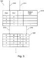
Figure 3 illustrates a permission mapping comprising two tables in accordance with an exemplary embodiment. - The illustration in the drawing is schematic. It is noted that in different figures, similar or identical elements are provided with the same reference signs or with reference signs, which differ only within the first digit.
-
Figure 1 shows a block diagram of amemory controller 100 according to an exemplary embodiment. Thecontroller 100 comprises amemory 110, aprocessing unit 120, aninput 130, and anoutput 140. Thememory 110 comprises data representing a set of equally sized logical regions in a logical address space, each logical region comprising a plurality of consecutive logical addresses. Thememory 110 further comprises data representing a mapping of a subset of consecutive logical addresses within each logical region to a set of physical addresses within a corresponding physical memory region, the subset of consecutive logical addresses comprising the first logical address within the logical region, said first logical address being mapped to a base address within the corresponding physical memory region. An example of the data inmemory 110 is shown inFigure 2 and will be discussed in further detail below. The processing unit is operable to access the memory (110) and is furthermore adapted to determine a physical address corresponding to any logical address based on the logical regions and the mapping. The logical address is received at theinput 130 and the determined physical address is output atoutput 140, preferably together with relevant permission data as will be discussed further below. -
Figure 2 illustrates amapping 200 between alogical address space 210 and aphysical memory 220 in accordance with an exemplary embodiment. In this exemplary embodiment, thelogical address space 210 comprises a set of equally sized logicalregions L# 0,L# 1, ...,L# 254,L# 255. Furthermore, the size of each logical region is 512 KB in this example. As the skilled person will readily appreciate, any number of regions and any region size is possible. - Thus, in customary hexadecimal notation, the first logical address of logical
region L# 0 is 0x0000:0000, the first logical address of logicalregion L# 1 is 0x0008:0000, and so forth. A subset (containing the first logical address) of each logical region is mapped to a corresponding physical memoryregion P# 0,P# 1, ...P# 255. The size of each physical region thus corresponds to the size of the subset and may thus vary between 0 (zero) and 512 KB. The parts of the logical regions, which are not included in the subsets, are hatched or shaded inFigure 2 . Themapping 200 contains respective links between the first logical address within each logical region and a base address within the corresponding physical memory region. More specifically, the link between the first logical address ofL# 0, i.e. 0x0000:0000, and the base address of physical memoryregion P# 0 is represented byarrow 201, the link between the first logical address ofL# 1, i.e. 0x0008:0000, and the base address of physical memoryregion P# 1 is represented byarrow 203, and the link between the first logical address of the next logical region (L#2, not shown), i.e. 0x0010:0000, and the base address of the corresponding physical memory region (P#2, not shown) is represented byarrow 205. In the example ofFigure 2 , logical regionL## 254 is empty and therefore botharrows region P# 255. Thearrows regions L# 0,L# 1 andL# 255 and the last physical addresses in physical memoryregions P# 0,P# 1 andP# 255. - Returning to
Figure 1 , theprocessing unit 120 is adapted to determine the physical address corresponding to a logical address received atinput 130 by identifying the logical region containing the logical address, determining an offset for the logical address relative to the first logical address within the identified logical region, identifying the base address within the corresponding physical memory region, and determining the physical address by adding the identified base address and the determined offset. Thus, referring again to the example shown inFigure 2 , if the logical address 0x000A:0000 is received atinput 130, then the processing unit determines (by dividing with the size of the logical regions) that this address lies within the logicalregion L# 1 and has an offset relative to the first logical address 0x0008:0000 of this logical region that is equal to 2:0000 (i.e. 131072 in decimal). Then, upon identifying the base address within corresponding physical memoryregion P# 1, the physical memory address corresponding to the received logical address is determined by adding the offset to the base address. - Summarizing the above, the physical memory (for example Flash or RAM) is first split into a number of logical regions located at fixed logical addresses and separated by large unmapped gaps. For example, there can be 256 logical regions, each with a fixed size of 512KB, and located at the following logical addresses:
- logical region L#0: 0x0000:0000 to 0x0007:FFFF
- logical region L#1: 0x0008:0000 to 0x000F:FFFF
- ...
- logical region L#254: 0x07F0:0000 to 0x07F7:FFFF
- logical region L#255: 0x07F8:0000 to 0x07FF:FFFF
- Each region can point to real physical memory at the start of the region and the rest of the region being unmapped. For example, if the mapping granularity is equal to 0.5KB, then the physical
region P# 0 can then be configured to contain 100.5KB out of the 512KB total logical size, the physicalregion P# 1, 23.5KB, etc. The granularity can depend on the memory type (e.g., 16 bytes for RAM and 512 bytes for Flash). - The
controller hardware 100 "compresses" the logical addresses into physical addresses that fit into the actual physical memory, as shown in the example ofFigure 2 and discussed above. Generally, the low order bits of the logical addresses,e.g. bits 0 to 18 inFig. 2 , are used to check that an access is made within the range of physical addresses allocated to that region, while the high order bits, e.g. bits 19 and above inFig. 2 , are used to determined which region to access. In other words, the size of the individual physical regions or physical address ranges,e.g. P# 0,P# 1, ...P# 255 inFig. 2 , which the logical addresses map to, are defined in the lower bits (bits 0 to 18 inFig. 2 ). - The
controller 100 makes use of an auxiliary RAM or registers containing the base physical addresses of each of the 256 logical regions. The controller applies the following formula to determine the physical address from the logical address: - region-number = logical_address[26:19]
- offset_in_region = logical_address[18:0]
-

- The logical regions provide at least the following two advantages:
Each region can be resized and populated independently of the other regions by just shifting the memory content and updating the value of each displacement above the region being resized. While this is a relatively heavy operation, in the typical secure element operating systems, it happens rarely, for example only during application installation or system updates. Furthermore, resizing a region does not change the logical address of existing content of the other regions, which is useful for independent update of an OS or of part of an OS. - The logical address space is very regular, which simplifies the permission system: it is indeed very fast in hardware to determine which is the region of a logical address and apply uniform permissions per region. This is to be compared to systems where the address space is more "compact" (no gaps), where fine-grained address comparators are needed, for example to achieve 32-byte granularity. This requires a lot of hardware resources, consumes more power, and will therefore always have a limited number of permission regions.
- The
memory 110 ofcontroller 100 may further comprise a permission mapping indicating whether each logical region is accessible to one or more of a plurality of execution contexts, in particular operating systems (OSs) and theprocessing unit 120 may further be adapted to determine whether a selected logical region is accessible for a selected execution contcxt.Figure 3 illustrates an exemplary permission mapping comprising two tables 310, 320 in accordance with such an exemplary embodiment. The first table 310 contains one entry or line for each region with indications of whether or not the corresponding region is accessible for each of the execution contexts Ctx0, Ctx1, ..., as well as an indication of a region type. The second table 320 contains one line or entry for each region type with indications of whether or not the corresponding region type has a read permission R, a write permission W, an execute permission X, and a privileged permission P. In operation, thecontroller 100 uses the two tables 310,320 as follows: For any current context of execution (as represented by arrow 312) and logical address to be checked (as represented by arrow 314), the first table 310 is used to determine whether access is allowed 1 or not allowed 0 for the current context of execution. The result us output at 316. Furthermore, the corresponding region type is identified and output at 318. Then, using the second table 320, the permission types corresponding to the identified region type are identified, i.e. it is determined whether each of a read permission R, a write permission W, an execute permission X, and a privileged permission P are given or not. The result may be output as a four-bit vector at 322. If access is denied in the first table, the vector may have thevalue 0000. - As shown above, the permission system makes use of two levels of permission tables 310, 320 to allow fast context switches between OSs with limited resource consumption;
- A first-level table (TABLE1 310) provides for each region:
- ∘ Whether the region is accessible to a set of "execution contexts", for example one context per OS
- ∘ A small token called the "region type". For example, the region type can be encoded on 5 bits, which allows up to 32 different region types
- A second-level table (TABLE2 320) provides four permission bits per region type (Read, Write, eXecute, Privileged).
- The described permission system has several advantages, including:
- The first table 310 (TABLE1) is relatively big (about 16 bits per region, i.e., 512 bytes for 256 regions) but only a single copy of the table is necessary because the overall access to the logical regions is static and may be changed only when the system configuration is updated
- The second table 320 (TABLE2) is compact (32x4 bits = 4 words), which allows a fast context-switch between OSs: the hypervisor must just reload these four words to context-switch the entire memory view of an OS
- Fine-grained permissions can be assigned per region type only, not per region, but there are still a relative high number of region types and they allow grouping multiple regions that share the same permissions. For example, all the code regions of an OS can share the same region type and still be separated in the logical address space, which allows separate updates of these parts
-
TABLE1 310 allows a region to be accessible to a single context or to multiple contexts, thus supporting private and shared regions - Furthermore, the described system is suitable for fast hardware implementation because:
-
TABLE2 320 is very small and can thus be implemented entirely in fast flip-flop registers - An extract of
TABLE1 310 can be kept in a fast cache (Translation Lookaside Buffer). This cache needs to be invalidated only whenTABLE1 310 changes. WhenTABLE2 320 is loaded, the content of the cache is still valid - Thanks to the logical region address system, the region number can be determined very quickly by extracting a few bits from the logical address (bits 26:19, for example).
- The initial motivation for embodiments of the present invention was to setup a system with two operating systems in a single device running a single processor core: (1) a Secure Element OS, taking care of payment, transport, and device security applications; and (2) a UICC OS, implementing the operations on behalf of a Mobile Network Operator.
- The virtualization system allows separate certifications of these two OSes and separate updates of them.
- Another motivation of the virtualization system is to isolate the implementation of the communication protocols in an OS that is separate from the main OS's. This is expected to simplify the certification of the JCOP OS as the communication protocol stacks would not need to be certified at the same level as the main JCOP OS.
- Another application of the system is to be able to host a third-party native OS alongside JCOP. This third-party OS would be able to run in Privileged mode, handle interrupts and interact with peripherals, under the control of the hypervisor.
- It is noted that, unless otherwise indicated, the use of terms such as "upper", "lower", "left", and "right" refers solely to the orientation of the corresponding drawing.
- It is noted that the term "comprising" does not exclude other elements or steps and that the use of the articles "a" or "an" does not exclude a plurality. Also, elements described in association with different embodiments may be combined. It should also be noted that reference signs in the claims should not be construed as limiting the scope of the claims.
Claims (15)
- A method of managing memory in an electronic device, the method comprising
creating a set of equally sized logical regions in a logical address space, each logical region comprising a plurality of consecutive logical addresses, and
mapping a subset of consecutive logical addresses within each logical region to a set of physical addresses within a corresponding physical memory region, the subset of consecutive logical addresses comprising the first logical address within the logical region, said first logical address being mapped to a base address within the corresponding physical memory region. - The method according to claim 1, further comprising
creating a permission mapping associating a permission type to each logical region and to each execution context of a plurality of execution contexts. - The method according to claim 2, wherein each execution context of the plurality of execution contexts corresponds to one of a plurality of operating systems.
- The method according to claim 2 or 3, wherein creating the permission mapping comprises
creating a first permission table indicating for each logical region whether or not the logical region is accessible to each of the plurality of execution contexts, the first permission table further indicating a region type for each logical region, and
creating a second permission table indicating for each region type whether each of a plurality of permission types is given or not. - The method according to claim 4, wherein the plurality of permission types comprises a read permission, a write permission, an execute permission, and a privileged permission.
- A controller (100) for managing memory in an electronic device, the controller comprising
a memory (110) comprisinga set of equally sized logical regions (L#0, L#1, L#254, L#255) in a logical address space (210), each logical region comprising a plurality of consecutive logical addresses, anda mapping (200) of a subset of consecutive logical addresses within each logical region to a set of physical addresses within a corresponding physical memory region (P#0, P#1, P#255), the subset of consecutive logical addresses comprising the first logical address within the logical region, said first logical address being mapped to a base address within the corresponding physical memory region, anda processing unit (120) operable to access the memory (110) and adapted to determine a physical address corresponding to any logical address based on the logical regions and the mapping. - The controller according to claim 6, wherein the processing unit is adapted to determine the physical address by
identifying the logical region containing the logical address,
determining an offset for the logical address relative to the first logical address within the identified logical region,
identifying the base address within the corresponding physical memory region, and determining the physical address by adding the identified base address and the determined offset. - The controller according to claim 6 or 7,
wherein the memory further comprises a permission mapping associating permission types to each logical region and to each execution context of a plurality of execution contexts, and
wherein the processing unit is further adapted to determine permission types for a selected logical region and a selected execution context. - The controller according to claim 8, wherein each execution context of the plurality of execution contexts corresponds to one of a plurality of operating systems.
- The controller according to claim 8 or 9,
wherein the permission mapping comprisesa first permission table indicating for each logical region whether or not the logical region is accessible to each of a plurality of execution contexts, the first permission table further indicating a region type for each logical region, anda second permission table indicating for each region type whether each of a plurality of permission types is given or not, andwherein the processing unit is further adapted to identify a region type corresponding to the selected logical region and to identify the permission types that are given for the identified region type. - The controller according to claim 10, wherein the plurality of permission types comprises a read permission, a write permission, an execute permission, and a privileged permission.
- A method of determining a physical address in a physical memory region using a controller, the controller comprising a memory comprising a set of equally sized logical regions in a logical address space, each logical region comprising a plurality of consecutive logical addresses, and a mapping of a subset of consecutive logical addresses within each logical region to a set of physical addresses within a corresponding physical memory region, the subset of consecutive logical addresses comprising the first logical address within the logical region, said first logical address being mapped to a base address within the corresponding physical memory region, the method comprising
receiving a logical address,
identifying the logical region containing the logical address,
determining an offset for the logical address relative to the first logical address within the identified logical region,
identifying the base address within the corresponding physical memory region, and
determining the physical address by adding the identified base address and the determined offset. - The method according to claim 12, wherein the memory further comprises a permission mapping associating permission types to each logical region and to each execution context of a plurality of execution contexts, the method further comprising
determining permission types for a selected logical region and a selected execution context. - The method according to claim 13, wherein each execution context of the plurality of execution contexts corresponds to one of a plurality of operating systems.
- The method according to claim 13 or 14, wherein the permission mapping comprises
a first permission table indicating for each logical region whether or not the logical region is accessible to each of a plurality of execution contexts, the first permission table further indicating a region type for each logical region, and
a second permission table indicating for each region type whether each of a plurality of permission types is given or not,
the method further comprising
identifying a region type corresponding to the selected logical region, and
identifying the permission types that are given for the identified region type.
Priority Applications (3)
| Application Number | Priority Date | Filing Date | Title |
|---|---|---|---|
| EP19290089.2A EP3792800A1 (en) | 2019-09-12 | 2019-09-12 | Managing equally sized virtual memory regions and physical memory regions in an electronic device |
| US16/996,448 US11269788B2 (en) | 2019-09-12 | 2020-08-18 | Managing memory in an electronic device |
| CN202010894122.5A CN112486855B (en) | 2019-09-12 | 2020-08-31 | Managing memory in electronic devices |
Applications Claiming Priority (1)
| Application Number | Priority Date | Filing Date | Title |
|---|---|---|---|
| EP19290089.2A EP3792800A1 (en) | 2019-09-12 | 2019-09-12 | Managing equally sized virtual memory regions and physical memory regions in an electronic device |
Publications (1)
| Publication Number | Publication Date |
|---|---|
| EP3792800A1 true EP3792800A1 (en) | 2021-03-17 |
Family
ID=68583289
Family Applications (1)
| Application Number | Title | Priority Date | Filing Date |
|---|---|---|---|
| EP19290089.2A Withdrawn EP3792800A1 (en) | 2019-09-12 | 2019-09-12 | Managing equally sized virtual memory regions and physical memory regions in an electronic device |
Country Status (3)
| Country | Link |
|---|---|
| US (1) | US11269788B2 (en) |
| EP (1) | EP3792800A1 (en) |
| CN (1) | CN112486855B (en) |
Citations (2)
| Publication number | Priority date | Publication date | Assignee | Title |
|---|---|---|---|---|
| WO2009088920A1 (en) * | 2007-12-31 | 2009-07-16 | Sandisk Il Ltd. | System, method and memory device providing data scrambling compatible with on-chip copy operation |
| WO2016203189A1 (en) * | 2015-06-16 | 2016-12-22 | Arm Limited | Secure initialisation |
Family Cites Families (22)
| Publication number | Priority date | Publication date | Assignee | Title |
|---|---|---|---|---|
| US7013379B1 (en) * | 2001-12-10 | 2006-03-14 | Incipient, Inc. | I/O primitives |
| WO2006027021A1 (en) | 2004-09-10 | 2006-03-16 | Freescale Semiconductor, Inc. | Memory management unit and a method for memory management |
| CN100533409C (en) * | 2005-07-29 | 2009-08-26 | 松下电器产业株式会社 | Memory controller, nonvolatile memory device, nonvolatile memory system, and nonvolatile memory address management method |
| US7543126B2 (en) * | 2005-08-31 | 2009-06-02 | International Business Machines Corporation | Apparatus, system, and method for implementing protected virtual memory subcontexts |
| US8572329B2 (en) | 2005-10-04 | 2013-10-29 | Arm Limited | Multi-region default memory map |
| US8095769B2 (en) | 2008-08-19 | 2012-01-10 | Freescale Semiconductor, Inc. | Method for address comparison and a device having address comparison capabilities |
| US8578126B1 (en) * | 2009-10-29 | 2013-11-05 | Netapp, Inc. | Mapping of logical start addresses to physical start addresses in a system having misalignment between logical and physical data blocks |
| US20140108701A1 (en) | 2010-07-16 | 2014-04-17 | Memory Technologies Llc | Memory protection unit in a virtual processing environment |
| EP2609511B1 (en) * | 2010-08-26 | 2016-10-19 | Freescale Semiconductor, Inc. | Memory management unit for a microprocessor system, microprocessor system and method for managing memory |
| US8719664B1 (en) * | 2011-04-12 | 2014-05-06 | Sk Hynix Memory Solutions Inc. | Memory protection cache |
| US8943251B2 (en) | 2012-05-14 | 2015-01-27 | Infineon Technologies Austria Ag | System and method for processing device with differentiated execution mode |
| GB2536880B (en) | 2015-03-24 | 2021-07-28 | Advanced Risc Mach Ltd | Memory management |
| DE102015210539A1 (en) | 2015-06-09 | 2016-12-15 | Robert Bosch Gmbh | Memory protection unit, memory management unit and microcontroller |
| KR20160150384A (en) * | 2015-06-22 | 2016-12-30 | 에스케이하이닉스 주식회사 | Data storage device and operating method thereof |
| US10255191B2 (en) * | 2015-08-13 | 2019-04-09 | Advanced Micro Devices, Inc. | Logical memory address regions |
| US9880939B2 (en) * | 2015-09-04 | 2018-01-30 | Toshiba Memory Corporation | Memory system and information processing system |
| KR102639670B1 (en) * | 2016-06-30 | 2024-02-26 | 에스케이하이닉스 주식회사 | Memory system and operation method for the same |
| JP2018116329A (en) * | 2017-01-16 | 2018-07-26 | 富士通株式会社 | Storage control apparatus and storage control program |
| JP2019008730A (en) * | 2017-06-28 | 2019-01-17 | 東芝メモリ株式会社 | Memory system |
| US10635331B2 (en) * | 2017-07-05 | 2020-04-28 | Western Digital Technologies, Inc. | Distribution of logical-to-physical address entries across bank groups |
| US10534718B2 (en) * | 2017-07-31 | 2020-01-14 | Micron Technology, Inc. | Variable-size table for address translation |
| KR20200022118A (en) * | 2018-08-22 | 2020-03-03 | 에스케이하이닉스 주식회사 | Data storage device and operating method thereof |
-
2019
- 2019-09-12 EP EP19290089.2A patent/EP3792800A1/en not_active Withdrawn
-
2020
- 2020-08-18 US US16/996,448 patent/US11269788B2/en active Active
- 2020-08-31 CN CN202010894122.5A patent/CN112486855B/en active Active
Patent Citations (3)
| Publication number | Priority date | Publication date | Assignee | Title |
|---|---|---|---|---|
| WO2009088920A1 (en) * | 2007-12-31 | 2009-07-16 | Sandisk Il Ltd. | System, method and memory device providing data scrambling compatible with on-chip copy operation |
| WO2016203189A1 (en) * | 2015-06-16 | 2016-12-22 | Arm Limited | Secure initialisation |
| US20180173645A1 (en) * | 2015-06-16 | 2018-06-21 | Arm Limited | Secure initialisation |
Non-Patent Citations (1)
| Title |
|---|
| ANONYMOUS: "Virtual memory - Wikipedia", 4 July 2019 (2019-07-04), XP093220707, Retrieved from the Internet <URL:https://en.wikipedia.org/w/index.php?title=Virtual_memory&oldid=904752041> [retrieved on 20241104] * |
Also Published As
| Publication number | Publication date |
|---|---|
| US20210081335A1 (en) | 2021-03-18 |
| CN112486855B (en) | 2025-01-07 |
| US11269788B2 (en) | 2022-03-08 |
| CN112486855A (en) | 2021-03-12 |
Similar Documents
| Publication | Publication Date | Title |
|---|---|---|
| CN113168379B (en) | Fast access to virtual machine memory backed by the host computer's virtual memory | |
| US8661181B2 (en) | Memory protection unit in a virtual processing environment | |
| CN113094700B (en) | System for performing safety operation and method for performing safety operation by system | |
| CN107783913B (en) | Resource access method applied to computer and computer | |
| US7620766B1 (en) | Transparent sharing of memory pages using content comparison | |
| US10176007B2 (en) | Guest code emulation by virtual machine function | |
| KR100914081B1 (en) | Guest to host address translation for devices to access memory in a partitioned system | |
| US8127098B1 (en) | Virtualization of real mode execution | |
| US20140108701A1 (en) | Memory protection unit in a virtual processing environment | |
| CN111316248B (en) | Facilitates access to information in local memory areas | |
| US8176142B2 (en) | Shared JAVA jar files | |
| EP3584708B1 (en) | Protection key management and prefixing in virtual address space legacy emulation system | |
| US10552309B2 (en) | Locality domain-based memory pools for virtualized computing environment | |
| US10331591B2 (en) | Logical-to-physical block mapping inside the disk controller: accessing data objects without operating system intervention | |
| US11573911B2 (en) | Memory access control | |
| KR20240004738A (en) | Techniques for restricting access to memory using capabilities | |
| US9600190B2 (en) | Virtual machine functions for multiple privileged pages | |
| KR20120070326A (en) | A apparatus and a method for virtualizing memory | |
| US20250284525A1 (en) | Software isolation of virtual machine resources | |
| US11900142B2 (en) | Improving memory access handling for nested virtual machines | |
| US20230185593A1 (en) | Virtual device translation for nested virtual machines | |
| US11269788B2 (en) | Managing memory in an electronic device | |
| US12019733B2 (en) | Compartment isolation for load store forwarding | |
| US20260037289A1 (en) | Enabling large frames for secure virtual machines | |
| WO2020033049A1 (en) | Fast initialization of complex in-memory data structures |
Legal Events
| Date | Code | Title | Description |
|---|---|---|---|
| PUAI | Public reference made under article 153(3) epc to a published international application that has entered the european phase |
Free format text: ORIGINAL CODE: 0009012 |
|
| STAA | Information on the status of an ep patent application or granted ep patent |
Free format text: STATUS: THE APPLICATION HAS BEEN PUBLISHED |
|
| AK | Designated contracting states |
Kind code of ref document: A1 Designated state(s): AL AT BE BG CH CY CZ DE DK EE ES FI FR GB GR HR HU IE IS IT LI LT LU LV MC MK MT NL NO PL PT RO RS SE SI SK SM TR |
|
| AX | Request for extension of the european patent |
Extension state: BA ME |
|
| STAA | Information on the status of an ep patent application or granted ep patent |
Free format text: STATUS: REQUEST FOR EXAMINATION WAS MADE |
|
| 17P | Request for examination filed |
Effective date: 20210917 |
|
| RBV | Designated contracting states (corrected) |
Designated state(s): AL AT BE BG CH CY CZ DE DK EE ES FI FR GB GR HR HU IE IS IT LI LT LU LV MC MK MT NL NO PL PT RO RS SE SI SK SM TR |
|
| STAA | Information on the status of an ep patent application or granted ep patent |
Free format text: STATUS: EXAMINATION IS IN PROGRESS |
|
| 17Q | First examination report despatched |
Effective date: 20241108 |
|
| STAA | Information on the status of an ep patent application or granted ep patent |
Free format text: STATUS: THE APPLICATION IS DEEMED TO BE WITHDRAWN |
|
| 18D | Application deemed to be withdrawn |
Effective date: 20250311 |