EP3792626A1 - Optical device and photoacoustic microscope - Google Patents
Optical device and photoacoustic microscope Download PDFInfo
- Publication number
- EP3792626A1 EP3792626A1 EP19799135.9A EP19799135A EP3792626A1 EP 3792626 A1 EP3792626 A1 EP 3792626A1 EP 19799135 A EP19799135 A EP 19799135A EP 3792626 A1 EP3792626 A1 EP 3792626A1
- Authority
- EP
- European Patent Office
- Prior art keywords
- light
- lens
- optical device
- axicon lens
- wavelength
- Prior art date
- Legal status (The legal status is an assumption and is not a legal conclusion. Google has not performed a legal analysis and makes no representation as to the accuracy of the status listed.)
- Granted
Links
Images












Classifications
-
- G—PHYSICS
- G01—MEASURING; TESTING
- G01N—INVESTIGATING OR ANALYSING MATERIALS BY DETERMINING THEIR CHEMICAL OR PHYSICAL PROPERTIES
- G01N29/00—Investigating or analysing materials by the use of ultrasonic, sonic or infrasonic waves; Visualisation of the interior of objects by transmitting ultrasonic or sonic waves through the object
- G01N29/04—Analysing solids
- G01N29/06—Visualisation of the interior, e.g. acoustic microscopy
- G01N29/0654—Imaging
- G01N29/0681—Imaging by acoustic microscopy, e.g. scanning acoustic microscopy
-
- G—PHYSICS
- G01—MEASURING; TESTING
- G01N—INVESTIGATING OR ANALYSING MATERIALS BY DETERMINING THEIR CHEMICAL OR PHYSICAL PROPERTIES
- G01N29/00—Investigating or analysing materials by the use of ultrasonic, sonic or infrasonic waves; Visualisation of the interior of objects by transmitting ultrasonic or sonic waves through the object
- G01N29/22—Details, e.g. general constructional or apparatus details
- G01N29/24—Probes
- G01N29/2418—Probes using optoacoustic interaction with the material, e.g. laser radiation, photoacoustics
-
- G—PHYSICS
- G01—MEASURING; TESTING
- G01N—INVESTIGATING OR ANALYSING MATERIALS BY DETERMINING THEIR CHEMICAL OR PHYSICAL PROPERTIES
- G01N29/00—Investigating or analysing materials by the use of ultrasonic, sonic or infrasonic waves; Visualisation of the interior of objects by transmitting ultrasonic or sonic waves through the object
- G01N29/22—Details, e.g. general constructional or apparatus details
- G01N29/28—Details, e.g. general constructional or apparatus details providing acoustic coupling, e.g. water
-
- G—PHYSICS
- G02—OPTICS
- G02B—OPTICAL ELEMENTS, SYSTEMS OR APPARATUS
- G02B27/00—Optical systems or apparatus not provided for by any of the groups G02B1/00 - G02B26/00, G02B30/00
- G02B27/30—Collimators
-
- G—PHYSICS
- G01—MEASURING; TESTING
- G01N—INVESTIGATING OR ANALYSING MATERIALS BY DETERMINING THEIR CHEMICAL OR PHYSICAL PROPERTIES
- G01N21/00—Investigating or analysing materials by the use of optical means, i.e. using sub-millimetre waves, infrared, visible or ultraviolet light
- G01N21/17—Systems in which incident light is modified in accordance with the properties of the material investigated
- G01N21/1702—Systems in which incident light is modified in accordance with the properties of the material investigated with opto-acoustic detection, e.g. for gases or analysing solids
- G01N2021/1706—Systems in which incident light is modified in accordance with the properties of the material investigated with opto-acoustic detection, e.g. for gases or analysing solids in solids
-
- G—PHYSICS
- G01—MEASURING; TESTING
- G01N—INVESTIGATING OR ANALYSING MATERIALS BY DETERMINING THEIR CHEMICAL OR PHYSICAL PROPERTIES
- G01N21/00—Investigating or analysing materials by the use of optical means, i.e. using sub-millimetre waves, infrared, visible or ultraviolet light
- G01N21/17—Systems in which incident light is modified in accordance with the properties of the material investigated
- G01N21/1702—Systems in which incident light is modified in accordance with the properties of the material investigated with opto-acoustic detection, e.g. for gases or analysing solids
-
- G—PHYSICS
- G02—OPTICS
- G02B—OPTICAL ELEMENTS, SYSTEMS OR APPARATUS
- G02B19/00—Condensers, e.g. light collectors or similar non-imaging optics
- G02B19/0004—Condensers, e.g. light collectors or similar non-imaging optics characterised by the optical means employed
- G02B19/0019—Condensers, e.g. light collectors or similar non-imaging optics characterised by the optical means employed having reflective surfaces only (e.g. louvre systems, systems with multiple planar reflectors)
-
- G—PHYSICS
- G02—OPTICS
- G02B—OPTICAL ELEMENTS, SYSTEMS OR APPARATUS
- G02B5/00—Optical elements other than lenses
- G02B5/001—Axicons, waxicons, reflaxicons
Definitions
- the present invention relates to an optical device and a photoacoustic microscope.
- Non-Patent Document 1 For example, a photoacoustic microscope is known that performs imaging by irradiating an object with light and detecting acoustic waves generated due to the radiated light (see Non-Patent Document 1, for example).
- Non-Patent Document 1 Bengal Rameez Chatni et al., "Functional photoacoustic microscopy of pH", Journal of Biomedical Optics, October 2011, Vol. 16(10), pp. 100503-1 to 100503-3
- condensation position does not differ due to the wavelength of the light. Furthermore, there are cases where it is preferable to have high light condensation.
- an optical device may comprise a first axicon lens to which collimated light is incident and which is configured to form diverging ring-shaped light.
- the optical device may comprise a lens to which the ring-shaped light formed by the first axicon lens is incident and which is configured to form ring-shaped collimated light.
- the optical device may comprise a condensing mirror that is configured to condense the ring-shaped collimated light formed by the lens.
- the optical device may further comprise a reflective collimator that collimates divergent light incident thereto, by reflecting the divergent light.
- the light collimated by the reflective collimator may become incident to the first axicon lens.
- the first axicon lens and the lens may be optically symmetric.
- the lens may be a second axicon lens with an apex angle that is substantially the same as an apex angle of the first axicon lens.
- the lens may be provided such that a conical surface of the lens faces a conical surface of the first axicon lens.
- the lens may be a convex lens in which a surface to which at least the ring-shaped light is incident has a convex curved surface approximating a conical surface of the first axicon lens.
- the lens may be provided such that the surface having the convex curved surface faces the conical surface of the first axicon lens.
- the condensing mirror and the lens may be provided integrally.
- the optical device may include a multi-wavelength light source. Light emitted by the multi-wavelength light source may be collimated and becomes incident to the first axicon lens.
- the photoacoustic microscope may include the optical device described above.
- the photoacoustic microscope may comprise a detector that is configured to detect an acoustic wave caused by light condensed by the condensing mirror.
- the detector may be configured to detect the acoustic wave that has propagated through air.
- the photoacoustic microscope may further comprise a processing apparatus that is configured to generate, based on the acoustic wave caused by light having a first wavelength condensed by the condensing mirror and the acoustic wave caused by light having a second wavelength, which is different from the light having the first wavelength condensed by the condensing mirror, an image of an object irradiated with the light having the first wavelength condensed by the condensing mirror and the light having the second wavelength.
- a processing apparatus that is configured to generate, based on the acoustic wave caused by light having a first wavelength condensed by the condensing mirror and the acoustic wave caused by light having a second wavelength, which is different from the light having the first wavelength condensed by the condensing mirror, an image of an object irradiated with the light having the first wavelength condensed by the condensing mirror and the light having the second wavelength.
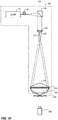
- Fig. 19 is a conceptual diagram showing a basic configuration of a photoacoustic microscope 700.
- the photoacoustic microscope 700 includes a laser 712, an optical fiber 714, a lens 720, a truncated cone prism 740, an acoustic wave sensor 760, and an amplifier 762.
- the lens 720 and the truncated cone prism 740 form an optical device for forming irradiation light that is radiated onto a target object 790.
- the laser 712 emits light to be radiated onto the target object 790.
- the light emitted by the laser 712 becomes incident to one end portion of the optical fiber 714 and is emitted as divergent light from the other end portion of the optical fiber 714.
- the divergent light emitted from the optical fiber 714 becomes incident to the lens 720.
- Diverging ring-shaped light is formed by the lens 720.
- the ring-shaped light formed by the lens 720 becomes incident to the truncated cone prism 740.
- the truncated cone prism 740 has a truncated cone shape.
- the ring-shaped light that has become incident to the truncated cone prism 740 is totally reflected by an internal side surface of the truncated cone prism 740.
- the irradiation light to be radiated onto the target object 790 is formed by the truncated cone prism 740.
- an acoustic wave is generated due to light absorption in a region of the target object 790 through which the irradiation light passes.
- the generated acoustic wave is propagated through water in a water tank 792 and reaches the acoustic wave sensor 760.
- the acoustic wave sensor 760 includes an acoustic lens, and generates an acoustic wave signal from the acoustic wave generated at the focal point position of the acoustic lens.
- the acoustic wave signal is supplied to the amplifier 762 as an electric signal and is amplified.
- the strength of the photoacoustic wave is calculated from the electric signal amplified by the amplifier 762 and converted into an image.
- the focal point of the lens 720 differs according to the wavelength, and therefore the condensation position of the irradiation light to be radiated on to the target object 790 differs according to the wavelength.
- the line 741 and the line 742 shown in Fig. 19 represent the inner surface on which the truncated cone prism 740 reflects the incident light.
- the light that has been totally reflected by the portion represented by the line 741 is substantially not condensed.
- the light that has been totally reflected by the portion represented by the line 742 is substantially not condensed. Therefore, according to the truncated cone prism 740, it is impossible to sufficiently increase the condensation amount of the irradiation light to be radiated onto the target object 790, and so the irradiation light diverges widely in a range outside the focal point position of the acoustic wave sensor 760. Therefore, the usage efficiency of the light energy generated by the laser 712 is lowered.
- Fig. 20 schematically shows a ray diagram of an example of an optical device 800 related to Fig. 19 .
- the optical device 800 includes a transparent collimator 810, an axicon lens 820, and a truncated cone prism 840.
- the combination of the transparent collimator 810 and the axicon lens 820 is an optical element corresponding to the lens 720 of Fig. 19 .
- the truncated cone prism 840, a target object 890, and a water tank 892 correspond respectively to the truncated cone prism 740, the target object 790, and the water tank 792.
- Fig. 21 shows the absorbed luminous flux per unit volume of light with a wavelength of 500 nm formed by the optical device 800.
- Fig. 22 shows the absorbed luminous flux per unit volume of light with a wavelength of 750 nm formed by the optical device 800.
- Fig. 23 shows the absorbed luminous flux per unit volume of light with a wavelength of 1000 nm formed by the optical device 800.
- Figs. 21 to 23 are distribution diagrams of the luminous flux collected by the target object.
- the vertical axes indicate the optical axis direction and the horizontal axes indicate a direction orthogonal to the optical axis.
- the condensation position in the optical axis direction substantially differs according to the wavelength, and that the position in the optical axis direction at which the absorbed luminous flux is at a maximum therefore differs according to the wavelength.
- the focal point of the transparent optical element differs according to the wavelength. Therefore, when light with different wavelengths is used in the optical device 800, a deviation occurs between the condensation positions in the optical axis direction according to the wavelengths, due to the light passing through the transparent collimator 810.
- the condensation amount of the light emitted from the optical device 800 can differ according to the wavelength.
- the width of the ring-shaped light incident to the truncated cone prism 840 becomes large, the condensation amount of the irradiation light to be radiated onto the target object becomes low, and therefore the resolution in the optical axis direction drops.
- the machining precision of a peak portion 825 of the conical surface 822 of the axicon lens 820 is lower than that of other portions, and therefore the light passing through the peak portion 825 is prone to scattering.
- the diameter of the light incident to the axicon lens 820 is reduced, the luminous flux density of the central portion of the incident light increases, and therefore the amount of luminous flux scattered at the peak portion 825 of the axicon lens 820 increases. Therefore, when the diameter of the light incident to the axicon lens 820 is reduced in order to increase the condensation amount of the irradiation light, the energy loss of the irradiation light increases.
- the condensation position differs according to the wavelength, which makes it necessary to adjust the condensation position, and this leads to a problem that it is impossible to quickly image a target object using many different wavelengths. Furthermore, there is a problem that it is not easy to sufficiently increase the condensation amount of the irradiation light.
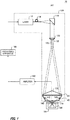
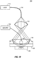
- Fig. 1 schematically shows a configuration of a photoacoustic microscope 10 according to an embodiment.
- the photoacoustic microscope 10 is a so-called AR-PAM (acoustic resolution photoacoustic microscope).
- the photoacoustic microscope 10 includes an optical device 100, an acoustic wave sensor 160, a transparent board 170, an amplifier 162, and a processing apparatus 180.
- the optical device 100 includes a laser 12, an optical fiber 14, a reflective collimator 110, an axicon lens 120, an axicon lens 130, and a condensing mirror 140.
- the laser 12 can generate laser light with different wavelengths.
- the laser 12 is an example of a multi-wavelength light source.
- the light emitted by the laser 12 is collimated and becomes incident to the axicon lens 120.
- the light generated by the laser 12 becomes incident to one end portion of the optical fiber 14 and is emitted as divergent light from the other end portion of the optical fiber 14.
- the reflective collimator 110 collimates the divergent light incident thereto, by reflecting this divergent light.
- the reflective collimator 110 has a reflective surface with a curved shape that collimates the divergent light. Since the reflective collimator 110 collimates the incident light using reflection, there is substantially no focal point deviation in the optical axis AX direction due to the wavelength.
- the light collimated by the reflective collimator 110 becomes incident to the axicon lens 120.
- the axicon lens 120 forms the diverging ring-shaped light from the light incident thereto.
- the ring-shaped light formed by the axicon lens 120 becomes incident to the axicon lens 130, and the axicon lens 130 forms ring-shaped collimated light.
- the collimated light formed by the axicon lens 130 may refer to light that is substantially collimated.
- the collimated light formed by the axicon lens 130 may refer to light with a higher degree of parallelism than the ring-shaped light incident to the axicon lens 130.
- the axicon lens 120 and the axicon lens 130 substantially have optical symmetry.
- the axicon lens 130 has substantially the same apex angle as the axicon lens 120.
- the apex angle of the axicon lens 130 is preferably substantially the same as the apex angle of the axicon lens 120.
- the apex angle of the axicon lens 130 may differ from the apex angle of the axicon lens 120, such that the axicon lens 130 can form the collimated light.
- the axicon lens 130 is provided such that a conical surface 132 of the axicon lens 130 faces a conical surface 122 of the axicon lens 120.
- the light collimated by the reflective collimator 110 becomes incident to the axicon lens 120 and the axicon lens 130, which are optically symmetric, to become collimated ring-shaped light.
- the light emitted from the axicon lens 130 can be collimated. It is possible for the inner diameter and the outer diameter of the ring-shaped collimated light emitted from the axicon lens 130 to differ according to the wavelength, but the difference in parallelism due to the wavelength is small.
- the condensing mirror 140 condenses the ring-shaped collimated light formed by the axicon lens 130.
- the condensing mirror 140 is a parabolic mirror, for example.
- the condensing mirror 140 has a reflective surface 142, represented by a parabolic rotating body, to condense the parallel light incident thereto into a point. In this way, the condensing mirror 140 can condense the ring-shaped collimated light formed by the axicon lens 130 at a specific position on the target object, using reflection. Since the condensing mirror 140 condenses the incident light using reflection, the condensation position and condensation amount do not substantially depend on the wavelength.
- the condensing mirror 140 is designed to converge the collimated light into a specific point no matter where on the reflective surface this collimated light is incident, the condensing mirror 140 can condense this light to the specific point even if the inner diameter and the outer diameter of the collimated light incident thereto differ due to the wavelength.
- the condensation amount is not substantially reduced even when the ring amplitude of the ring-shaped collimated light incident thereto increases, and therefore it is possible to increase the diameter of the collimated light incident to the axicon lens 120.
- the diameter of the collimated light incident to the axicon lens 120 it is possible to reduce the amount of luminous flux scattered by a peak portion 125 of the axicon lens 120. Therefore, it is possible to reduce the energy loss of the irradiation light. In this way, it is possible to increase the usage efficiency of the light energy generated by the laser 12.
- the acoustic wave sensor 160 is fixed to the transparent board 170.
- the transparent board 170 is provided between the condensing mirror 140 and a target object 190.
- the acoustic wave sensor 160 is provided to be acoustically coupled to the target object 190.
- the acoustic wave sensor 160 is provided to contact water 194, which serves as an acoustic matching material.
- the transparent board 170 may be provided in contact with the water 194.
- the transparent board 170 is formed of a material that transparently passes the light emitted by the laser 12. The light from the condensing mirror 140 becomes incident to the target object 190, through a region around the acoustic wave sensor 160.
- the acoustic wave sensor 160 and the optical device 100 are positionally aligned such that the condensation position of the light from the condensing mirror 140 to the target object 190 and the focal point position of the acoustic lens of the acoustic wave sensor 160 match.
- the acoustic wave sensor 160 and the optical device 100 are positionally aligned by adjusting the position of the transparent board 170 in the optical axis AX direction and in a direction orthogonal to the optical axis AX.
- the optical device 100 it is possible to independently adjust the positions of the optical device 100 and the acoustic wave sensor 160, and therefore it is easy to positionally align the focal point of the optical device 100 and the focal point of the acoustic wave sensor 160.
- an acoustic wave is generated from a specific position corresponding to the condensation position in the target object 190.
- the generated acoustic wave passes through the water 194 to arrive at the acoustic wave sensor 160.
- the acoustic wave sensor 160 generates an acoustic wave signal by detecting the acoustic wave generated at the focal point position of the acoustic lens.
- the acoustic wave signal is supplied to the amplifier 162 as an electric signal and amplified, and is then supplied to the processing apparatus 180.
- the processing apparatus 180 calculates the strength of the photoacoustic wave of the target object 190 from the electrical signal amplified by the amplifier 162.
- the processing apparatus 180 acquires an image of the target object 190 by measuring the photoacoustic wave while moving the target object 190 and the optical device 100 relative to each other in a plane orthogonal to the optical axis AX.
- the processing apparatus 180 Based on an acoustic wave caused by light having a first wavelength condensed by the condensing mirror 140 and an acoustic wave caused by light having a second wavelength that is different from the light having the first wavelength condensed by the condensing mirror 140, the processing apparatus 180 generates the image of the target object 190 that has been irradiated with the light having the first wavelength that has been condensed by the condensing mirror 140 and the light having the second wavelength.
- the processing apparatus 180 switches between generating light having the first wavelength that is absorbed by arteries and veins and light having the second wavelength, for which the ratio between the absorption coefficient for arteries and the absorption coefficient for veins differs from that of the light having the first wavelength, from the laser 12.
- the processing apparatus 180 generates the blood vessel image in which the arteries and veins are distinguished from each other, by detecting the arteries and veins at each position in a living body based on the magnitude of the photoacoustic wave detected by the acoustic wave sensor 160.
- the deviation of the condensation position in the optical axis AX direction due to the wavelength is small, and therefore there is no need to adjust the condensation position for each wavelength. Therefore, it is possible to detect the acoustic wave by switching the wavelength of the light irradiating the target object 190 at high speed. Accordingly, it is possible to quickly acquire the image of the target object 190 using light with many wavelengths.
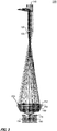
- Fig. 2 is a perspective view schematically showing an arrangement of optical elements included in an optical device 200, as an example of the present embodiment, along with the target object 190.
- Fig. 3 schematically shows a ray diagram in the optical device 200.
- the optical device 200 differs from the optical device 100 by including a convex lens 230 instead of the axicon lens 130 that is included in the optical device 100.
- the convex lens 230 includes a surface 232 that has a convex curved surface 233.
- the convex lens 230 is provided such that the surface 232 faces the conical surface 122 of the axicon lens 120.
- the light formed by the axicon lens 120 becomes incident to the convex curved surface 233, but does not enter farther to the AX side than the convex curved surface 233.
- the convex curved surface 233 has a shape that approximates the conical surface 122 of the axicon lens 120.
- “approximates” may mean that, for example, in a region of the convex curved surface 233 where the light from the axicon lens 120 is incident, the difference between the apex angle of the conical surface formed by a tangent that touches the convex curved surface 233 and intersects the optical axis at a specific angle and the apex angle of the conical surface 122 of the axicon lens 120 is within a predetermined range.
- the "predetermined range” may be determined from the tolerable error of the collimation amount demanded of the convex lens 230.
- Fig. 4 shows an absorbed luminous flux amount per unit volume of light having a wavelength of 500 nm formed by the optical device 200.
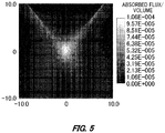
- Fig. 5 shows an absorbed luminous flux amount per unit volume of light having a wavelength of 750 nm formed by the optical device 200.
- Fig. 6 shows an absorbed luminous flux amount per unit volume of light having a wavelength of 1000 nm formed by the optical device 200.
- the vertical axes indicate the optical axis direction AX and the horizontal axes indicate a direction orthogonal to the optical axis AX, in the same manner as in the distribution diagrams of the absorbed luminous flux amount shown in Figs. 21 to 23 .
- the axicon lens As described above, by including the axicon lens, the lens that is substantially or approximately optically symmetric to the axicon lens, and the condensing mirror, it is possible to provide an optical device in which the deviation of the condensation position in the optical axis direction due to the wavelength is small. Furthermore, it is possible to provide an optical device with high condensation.
- the convex lens 230 shown in Figs. 2 and 3 may have a convex shape across the entire surface facing the conical surface 122 of the axicon lens 120.
- the convex lens 230 only needs to include at least the convex curved surface 233 in the region where the light from the axicon lens 120 is incident, and other regions may have any shape.
- a lens may be used that has a surface optically symmetric to the conical surface of the axicon lens 120, at least in a region where the light from the axicon lens 120 is incident.
- a lens may be used that has a conical surface only in a peripheral portion of the axicon lens 130.
- the axicon lens 130 as well only needs to include a surface that is optically symmetric to at least the axicon lens 120 in the region where the light from the axicon lens 120 is incident, and other regions may have any shape.
- Fig. 7 is a cross-sectional diagram of an optical element 500, as a modification of the axicon lens 130 and the condensing mirror 140.
- the optical element 500 is single optical element in which the axicon lens 130 and the condensing mirror 140 are provided integrally.
- the optical element 500 has the effects of the axicon lens 130 and the condensing mirror 140.
- the optical element 500 includes an axicon lens portion 530 and a condensing mirror portion 540.
- the axicon lens portion 530 has a conical surface 532 on a peripheral portion thereof.
- the condensing mirror portion 540 has a parabolic surface 542, which is a reflective surface with a parabolic shape.
- the optical element 500 is provided such that the conical surface 532 faces the conical surface 122 of the axicon lens 120.
- the conical surface 532 of the axicon lens portion 530 has the effect of the conical surface 132 of the axicon lens 130.
- the parabolic surface 542 of the condensing mirror portion 540 has the effect of the reflective surface 142 of the condensing mirror 140.
- the axicon lens 130 is arranged such that the conical surface of the axicon lens 130 faces the conical surface of the axicon lens 120.
- the axicon lens 120 may be arranged such that the conical surface 122 faces the reflective collimator 110, and the axicon lens 130 may be arranged such that the floor surface of the axicon lens 130 faces the floor surface of the axicon lens 120.
- Fig. 8 shows a cross section of the axicon lens 120 and an axicon lens 630.
- the axicon lens 630 has a conical surface 632, corresponding to the conical surface 132 of the axicon lens 130, at a peripheral portion thereof, and has the same effect as the axicon lens 130.
- the axicon lens 120 is arranged such that the conical surface 122 faces the reflective collimator 110, and the axicon lens 630 is arranged such that a floor surface 633 faces a floor surface 123 of the axicon lens 120.
- the axicon lens 120 is arranged such that the conical surface 122 faces the reflective collimator 110, and the convex lens 230 is arranged such that a floor surface of the convex lens 230 faces the floor surface of the axicon lens 120.
- the target object 190 is not limited to being a blood vessel or blood component.
- Various light-absorbing materials inside living organisms can be used as the target object 190.
- various objects that absorb light, and not just those in living organisms can be used as the target object 190.
- industrial products with joints made of different types of material may be used as target objects 190, and the photoacoustic microscope 10 may be used as an inspection apparatus for delamination of the joints made of different types of material.
- Fig. 9 schematically shows the configuration of a photoacoustic microscope 20 according to another embodiment.
- the photoacoustic microscope 20 is an AR-PAM, in the same manner as the photoacoustic microscope 10.
- the photoacoustic microscope 20 includes the optical device 100, the acoustic wave sensor 160, the amplifier 162, and the processing apparatus 180.
- configurational elements of the photoacoustic microscope 20 configurational elements that are the same as those of the photoacoustic microscope 10 are given the same reference numerals.
- the photoacoustic microscope 20 differs from the photoacoustic microscope 10 in that the acoustic wave sensor 160 and the target object 190 are acoustically coupled without using water as the acoustic coupling medium.
- the acoustic wave sensor 160 is acoustically coupled to the target object 190 via gas in the air, for example. Accordingly, the acoustic wave sensor 160 detects the acoustic wave generated by the light condensed by the condensing mirror 140 and propagated through the air.
- a liquid other than water or any gas other than air may be used as the acoustic coupling medium.
- a solid that transparently passes the light generated by the laser 12 may be used as the acoustic coupling medium.
- the acoustic coupling medium may be a living organism.
- the photoacoustic microscope 20 does not need to include the transparent board 170 as the acoustic wave sensor 160 holding means.
- a means other than the transparent board 170 can be used as the acoustic wave sensor 160 holding means, as long as it is capable of holding the acoustic wave sensor 160 in a manner that does not obstruct the light headed from the condensing mirror 140 toward the target object 190.
- Fig. 10 schematically shows an experimental system for measuring a beam diameter of the emission light of the optical device 100.
- the experimental system includes ground glass 310 to which the emission light of the optical device 100 is incident and an imaging apparatus 320 that captures an image of the ground glass 310.
- the ground glass 310 is provided between the condensing mirror 140 and the imaging apparatus 320.
- the ground glass 310 is provided such that the position thereof in the optical axis AX direction from the condensing mirror 140 is adjustable.
- the imaging apparatus 320 is a camera that includes a CMOS image sensor.
- the imaging apparatus 320 is provided such that the imaging optical axis thereof matches the optical axis AX.
- the imaging apparatus 320 captures an image in a state where the ground glass 310 is focused on.
- the imaging apparatus 320 captures an image of the ground glass 310 in a state where laser light with a specific wavelength has been generated from the laser 12, and the diameter of a bright portion of the obtained image is measured as the beam diameter of the emission light of the optical device 100.
- the diameter of the bright portion is expressed in units of pixels forming the imaging acquired by the imaging apparatus 320.
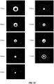
- Fig. 11 shows images captured in a state where laser light with a wavelength of 405 nm has been generated. The numerical value shown near each image indicates the position in the optical axis AX direction.
- Fig. 12 shows images captured in a state where laser light with a wavelength of 808 nm has been generated. The numerical value shown near each image indicates the position in the optical axis AX direction.
- both the light with a wavelength of 405 nm and the light with a wavelength of 808 nm are condensed near a position of 9.5 mm in the optical axis AX direction.
- the deviation of the condensation position in the optical axis AX direction due to the wavelength is extremely small.
- the emission light from the optical device 100 is completely ring-shaped, and therefore the bright portion of the image is also ring-shaped.
- a bright portion also occurs in the center of the ring-shaped bright portion, as shown in the images at the position of 11.5 mm in Figs. 11 and 12 , for example.
- This bright portion inside the ring-shaped bright portion is thought to occur due to the effect of machining efficiency of the peak portions of the axicon lens 120 and the axicon lens 130.
- the peak portions of the axicon lens 120 and the axicon lens 130 are rounded when viewed finely, and not perfect points, it is thought that the bright portion inside the ring-shaped bright portion occurs due to the light scattered by the peak portions of the axicon lens 120 and the axicon lens 130. Accordingly, when calculating the beam diameter from the bright portion, the bright portion inside the ring-shaped bright portion is not taken into account.
- Fig. 13 shows binary images obtained by binarizing the images captured in a state where the laser light with a wavelength of 405 nm has been generated.
- the numerical value near each binary image shows the position in the optical axis AX direction.
- Fig. 14 shows binary images obtained by binarizing the images captured in a state where the laser light with a wavelength of 808 nm has been generated.
- the numerical value near each binary image shows the position in the optical axis AX direction.
- Fig. 15 shows a profile of the emission light of the optical device 100.
- the horizontal axis indicates the beam diameter
- the vertical axis indicates the position in the optical axis AX direction.
- the beam diameter is calculated from the outer diameter of the bright portion in the binary image. As described above, the size of the beam diameter is expressed in pixel units.
- the light with a wavelength of 405 nm and the light with a wavelength of 808 nm emitted from the optical device 100 have approximately the same profile. Accordingly, it is understood that with the optical device 100, the deviation of the condensation positions in the optical axis direction and the difference in condensation amounts between the light with a wavelength of 405 nm and the light with a wavelength of 808 nm are both extremely small.
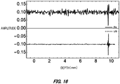
- Fig. 16 is a graph showing the results of a verification experiment of the photoacoustic measurement by the photoacoustic microscope 10. This verification experiment was performed by using a metal member having a surface that has undergone black alumite processing as the target object 190 in the photoacoustic microscope 10 shown in Fig. 1 , and making a comparison between the measurement result of an ultrasonic wave signal detected by the acoustic wave sensor 160 when the surface of the member was irradiated with light from the optical device 100 and the measurement result of an ultrasonic wave signal detected by the acoustic wave sensor 160 when the an ultrasonic wave was generated from the acoustic wave sensor 160.
- the vertical axis indicates the signal strength of the ultrasonic wave detected by the acoustic wave sensor 160.
- the horizontal axis indicates the position of the source generating the ultrasonic wave.
- PA indicates the positional dependency of the ultrasonic wave signal obtained when the metal member was irradiated with light.
- US indicates the positional dependency of the ultrasonic wave signal obtained when the ultrasonic wave signal was generated from the acoustic wave sensor 160.
- the horizontal axis of the US graph indicates a value obtained by converting the ultrasonic wave propagation time into a position in the optical axis AX direction, using the propagation speed of an ultrasonic wave in water.
- the peak position of the ultrasonic wave signal obtained when the metal member was irradiated with light approximately matches the peak position of the ultrasonic wave signal obtained when the ultrasonic wave was generated from the acoustic wave sensor 160. Accordingly, it was possible to verify that the ultrasonic wave signal measured when the metal member was irradiated with light is the photoacoustic wave generated by the metal member.
- Fig. 17 shows a photoacoustic image of metal mesh obtained by the photoacoustic microscope 10.
- Fig. 17 is a photoacoustic image in a case where metal mesh (line diameter of 0.18 mm and mesh interval of 0.51 mm) made of SUS 304 is used as the target object 190.
- the wavelength of the laser 12 used to obtain the photoacoustic image is 1064 nm, and the central frequency of the acoustic wave sensor 160 is 15 MHz.
- Fig. 18 shows a visible light image of the metal mesh serving as the target object 190.
- the portions having a high concentration in Fig. 17 indicate portions where the metal mesh is present.
Landscapes
- Physics & Mathematics (AREA)
- General Physics & Mathematics (AREA)
- Optics & Photonics (AREA)
- Biochemistry (AREA)
- Chemical & Material Sciences (AREA)
- Analytical Chemistry (AREA)
- Life Sciences & Earth Sciences (AREA)
- General Health & Medical Sciences (AREA)
- Health & Medical Sciences (AREA)
- Immunology (AREA)
- Pathology (AREA)
- Acoustics & Sound (AREA)
- Investigating Or Analyzing Materials By The Use Of Ultrasonic Waves (AREA)
- Ultra Sonic Daignosis Equipment (AREA)
- Investigating Or Analysing Materials By Optical Means (AREA)
Abstract
Description
- The present invention relates to an optical device and a photoacoustic microscope.
- Technology is known for performing imaging based on a response of an object caused by irradiating the object with light. For example, a photoacoustic microscope is known that performs imaging by irradiating an object with light and detecting acoustic waves generated due to the radiated light (see Non-Patent
Document 1, for example). - Non-Patent Document 1: Muhammad Rameez Chatni et al., "Functional photoacoustic microscopy of pH", Journal of Biomedical Optics, October 2011, Vol. 16(10), pp. 100503-1 to 100503-3
- In a device that uses condensed light, such as a photoacoustic microscope or the like, there are cases where it is preferable that the condensation position does not differ due to the wavelength of the light. Furthermore, there are cases where it is preferable to have high light condensation.
- In a first aspect of the present invention, provided is an optical device. The optical device may comprise a first axicon lens to which collimated light is incident and which is configured to form diverging ring-shaped light. The optical device may comprise a lens to which the ring-shaped light formed by the first axicon lens is incident and which is configured to form ring-shaped collimated light. The optical device may comprise a condensing mirror that is configured to condense the ring-shaped collimated light formed by the lens.
- The optical device may further comprise a reflective collimator that collimates divergent light incident thereto, by reflecting the divergent light. The light collimated by the reflective collimator may become incident to the first axicon lens.
- The first axicon lens and the lens may be optically symmetric.
- The lens may be a second axicon lens with an apex angle that is substantially the same as an apex angle of the first axicon lens.
- The lens may be provided such that a conical surface of the lens faces a conical surface of the first axicon lens.
- The lens may be a convex lens in which a surface to which at least the ring-shaped light is incident has a convex curved surface approximating a conical surface of the first axicon lens.
- The lens may be provided such that the surface having the convex curved surface faces the conical surface of the first axicon lens.
- The condensing mirror and the lens may be provided integrally.
- The optical device may include a multi-wavelength light source. Light emitted by the multi-wavelength light source may be collimated and becomes incident to the first axicon lens.
- According to a second embodiment, provided is a photoacoustic microscope. The photoacoustic microscope may include the optical device described above. The photoacoustic microscope may comprise a detector that is configured to detect an acoustic wave caused by light condensed by the condensing mirror.
- The detector may be configured to detect the acoustic wave that has propagated through air.
- The photoacoustic microscope may further comprise a processing apparatus that is configured to generate, based on the acoustic wave caused by light having a first wavelength condensed by the condensing mirror and the acoustic wave caused by light having a second wavelength, which is different from the light having the first wavelength condensed by the condensing mirror, an image of an object irradiated with the light having the first wavelength condensed by the condensing mirror and the light having the second wavelength.
- The summary clause does not necessarily describe all necessary features of the embodiments of the present invention. The present invention may also be a sub-combination of the features described above.
-
-
Fig. 1 schematically shows a configuration of aphotoacoustic microscope 10 according to an embodiment. -
Fig. 2 is a perspective view schematically showing an arrangement of optical elements included in anoptical device 200, as an example, along with thetarget object 190. -
Fig. 3 schematically shows a ray diagram in theoptical device 200. -
Fig. 4 shows an absorbed luminous flux amount per unit volume of light having a wavelength of 500 nm formed by theoptical device 200. -
Fig. 5 shows an absorbed luminous flux amount per unit volume of light having a wavelength of 750 nm formed by theoptical device 200. -
Fig. 6 shows an absorbed luminous flux amount per unit volume of light having a wavelength of 1000 nm formed by theoptical device 200. -
Fig. 7 is a cross-sectional diagram of anoptical element 500, as a modification of theaxicon lens 130 and thecondensing mirror 140. -
Fig. 8 is a cross-sectional view of an example of another exemplary arrangement of the axicon lens. -
Fig. 9 schematically shows the configuration of aphotoacoustic microscope 20 according to another embodiment. -
Fig. 10 schematically shows an experimental system for measuring a beam diameter of the emission light of theoptical device 100. -
Fig. 11 shows images captured in a state where laser light with a wavelength of 405 nm has been generated. -
Fig. 12 shows images captured in a state where laser light with a wavelength of 808 nm has been generated. -
Fig. 13 shows binary images obtained by binarizing the images captured in a state where the laser light with a wavelength of 405 nm has been generated. -
Fig. 14 shows binary images obtained by binarizing the images captured in a state where the laser light with a wavelength of 808 nm has been generated. -
Fig. 15 shows a profile of the emission light of theoptical device 100. -
Fig. 16 is a graph showing the results of a verification experiment of the photoacoustic measurement by thephotoacoustic microscope 10. -
Fig. 17 shows a photoacoustic image of metal mesh obtained by thephotoacoustic microscope 10. -
Fig. 18 shows a visible light image of the metal mesh serving as thetarget object 190. -
Fig. 19 is a conceptual diagram showing a basic configuration of aphotoacoustic microscope 700. -
Fig. 20 schematically shows a ray diagram of an example of anoptical device 800 related toFig. 19 . -
Fig. 21 shows the absorbed luminous flux per unit volume of light with a wavelength of 500 nm formed by theoptical device 800. -
Fig. 22 shows the absorbed luminous flux per unit volume of light with a wavelength of 750 nm formed by theoptical device 800. -
Fig. 23 shows the absorbed luminous flux per unit volume of light with a wavelength of 1000 nm formed by theoptical device 800. - Hereinafter, some embodiments of the present invention will be described, but the embodiments do not limit the invention according to the claims. All the combinations of the features described in the embodiments are not necessarily essential to means provided by aspects of the invention.
- First, the basic configuration of an optical device for a photoacoustic microscope will be described.
Fig. 19 is a conceptual diagram showing a basic configuration of aphotoacoustic microscope 700. Thephotoacoustic microscope 700 includes alaser 712, anoptical fiber 714, alens 720, atruncated cone prism 740, anacoustic wave sensor 760, and anamplifier 762. Thelens 720 and thetruncated cone prism 740 form an optical device for forming irradiation light that is radiated onto atarget object 790. - The
laser 712 emits light to be radiated onto thetarget object 790. The light emitted by thelaser 712 becomes incident to one end portion of theoptical fiber 714 and is emitted as divergent light from the other end portion of theoptical fiber 714. The divergent light emitted from theoptical fiber 714 becomes incident to thelens 720. Diverging ring-shaped light is formed by thelens 720. The ring-shaped light formed by thelens 720 becomes incident to thetruncated cone prism 740. - The
truncated cone prism 740 has a truncated cone shape. The ring-shaped light that has become incident to thetruncated cone prism 740 is totally reflected by an internal side surface of thetruncated cone prism 740. The irradiation light to be radiated onto thetarget object 790 is formed by thetruncated cone prism 740. - Due to the irradiation light from the
truncated cone prism 740 becoming incident to thetarget object 790, an acoustic wave is generated due to light absorption in a region of thetarget object 790 through which the irradiation light passes. The generated acoustic wave is propagated through water in awater tank 792 and reaches theacoustic wave sensor 760. Theacoustic wave sensor 760 includes an acoustic lens, and generates an acoustic wave signal from the acoustic wave generated at the focal point position of the acoustic lens. The acoustic wave signal is supplied to theamplifier 762 as an electric signal and is amplified. The strength of the photoacoustic wave is calculated from the electric signal amplified by theamplifier 762 and converted into an image. - In the
photoacoustic microscope 700, when the irradiation light to be radiated onto thetarget object 790 is formed using light with different wavelengths, the focal point of thelens 720 differs according to the wavelength, and therefore the condensation position of the irradiation light to be radiated on to thetarget object 790 differs according to the wavelength. - Furthermore, the
line 741 and theline 742 shown inFig. 19 represent the inner surface on which thetruncated cone prism 740 reflects the incident light. The light that has been totally reflected by the portion represented by theline 741 is substantially not condensed. Similarly, the light that has been totally reflected by the portion represented by theline 742 is substantially not condensed. Therefore, according to thetruncated cone prism 740, it is impossible to sufficiently increase the condensation amount of the irradiation light to be radiated onto thetarget object 790, and so the irradiation light diverges widely in a range outside the focal point position of theacoustic wave sensor 760. Therefore, the usage efficiency of the light energy generated by thelaser 712 is lowered. -
Fig. 20 schematically shows a ray diagram of an example of anoptical device 800 related toFig. 19 . Theoptical device 800 includes atransparent collimator 810, anaxicon lens 820, and atruncated cone prism 840. In theoptical device 800, the combination of thetransparent collimator 810 and theaxicon lens 820 is an optical element corresponding to thelens 720 ofFig. 19 . Thetruncated cone prism 840, atarget object 890, and awater tank 892 correspond respectively to thetruncated cone prism 740, thetarget object 790, and thewater tank 792. -
Fig. 21 shows the absorbed luminous flux per unit volume of light with a wavelength of 500 nm formed by theoptical device 800.Fig. 22 shows the absorbed luminous flux per unit volume of light with a wavelength of 750 nm formed by theoptical device 800.Fig. 23 shows the absorbed luminous flux per unit volume of light with a wavelength of 1000 nm formed by theoptical device 800. -
Figs. 21 to 23 are distribution diagrams of the luminous flux collected by the target object. In the distribution diagrams ofFigs. 21 to 23 , the vertical axes indicate the optical axis direction and the horizontal axes indicate a direction orthogonal to the optical axis. As shown inFigs. 21 to 23 , it is understood that the condensation position in the optical axis direction substantially differs according to the wavelength, and that the position in the optical axis direction at which the absorbed luminous flux is at a maximum therefore differs according to the wavelength. - In general, since the refractive index of the optical material differs according to the wavelength, the focal point of the transparent optical element differs according to the wavelength. Therefore, when light with different wavelengths is used in the
optical device 800, a deviation occurs between the condensation positions in the optical axis direction according to the wavelengths, due to the light passing through thetransparent collimator 810. - Furthermore, even in a case where the
transparent collimator 810 can substantially collimate light having a specific wavelength, there are cases where thetransparent collimator 810 cannot collimate light having other wavelengths to the same degree. Therefore, the condensation amount of the light emitted from theoptical device 800 can differ according to the wavelength. - Furthermore, in the
optical device 800, when the width of the ring-shaped light incident to thetruncated cone prism 840 becomes large, the condensation amount of the irradiation light to be radiated onto the target object becomes low, and therefore the resolution in the optical axis direction drops. In order to increase the condensation amount of the irradiation light, it is necessary to reduce the width of the ring-shaped light incident to thetruncated cone prism 840, and in order to achieve this, it is necessary to reduce the diameter of the light incident to theaxicon lens 820. However, in general, the machining precision of apeak portion 825 of theconical surface 822 of theaxicon lens 820 is lower than that of other portions, and therefore the light passing through thepeak portion 825 is prone to scattering. When the diameter of the light incident to theaxicon lens 820 is reduced, the luminous flux density of the central portion of the incident light increases, and therefore the amount of luminous flux scattered at thepeak portion 825 of theaxicon lens 820 increases. Therefore, when the diameter of the light incident to theaxicon lens 820 is reduced in order to increase the condensation amount of the irradiation light, the energy loss of the irradiation light increases. - As described in relation to
Figs. 19 to 23 , with the basic configuration of the optical device in the photoacoustic microscope, the condensation position differs according to the wavelength, which makes it necessary to adjust the condensation position, and this leads to a problem that it is impossible to quickly image a target object using many different wavelengths. Furthermore, there is a problem that it is not easy to sufficiently increase the condensation amount of the irradiation light. -
Fig. 1 schematically shows a configuration of aphotoacoustic microscope 10 according to an embodiment. Thephotoacoustic microscope 10 is a so-called AR-PAM (acoustic resolution photoacoustic microscope). Thephotoacoustic microscope 10 includes anoptical device 100, anacoustic wave sensor 160, atransparent board 170, anamplifier 162, and aprocessing apparatus 180. Theoptical device 100 includes alaser 12, anoptical fiber 14, areflective collimator 110, anaxicon lens 120, anaxicon lens 130, and acondensing mirror 140. - The
laser 12 can generate laser light with different wavelengths. Thelaser 12 is an example of a multi-wavelength light source. The light emitted by thelaser 12 is collimated and becomes incident to theaxicon lens 120. - Specifically, the light generated by the
laser 12 becomes incident to one end portion of theoptical fiber 14 and is emitted as divergent light from the other end portion of theoptical fiber 14. Thereflective collimator 110 collimates the divergent light incident thereto, by reflecting this divergent light. Specifically, thereflective collimator 110 has a reflective surface with a curved shape that collimates the divergent light. Since thereflective collimator 110 collimates the incident light using reflection, there is substantially no focal point deviation in the optical axis AX direction due to the wavelength. - The light collimated by the
reflective collimator 110 becomes incident to theaxicon lens 120. Theaxicon lens 120 forms the diverging ring-shaped light from the light incident thereto. - The ring-shaped light formed by the
axicon lens 120 becomes incident to theaxicon lens 130, and theaxicon lens 130 forms ring-shaped collimated light. Here, the collimated light formed by theaxicon lens 130 may refer to light that is substantially collimated. The collimated light formed by theaxicon lens 130 may refer to light with a higher degree of parallelism than the ring-shaped light incident to theaxicon lens 130. - As an example, the
axicon lens 120 and theaxicon lens 130 substantially have optical symmetry. Specifically, theaxicon lens 130 has substantially the same apex angle as theaxicon lens 120. In a case where the refractive index of theaxicon lens 130 is the same as the refractive index of theaxicon lens 120, the apex angle of theaxicon lens 130 is preferably substantially the same as the apex angle of theaxicon lens 120. However, if the refractive index of theaxicon lens 130 differs from the refractive index of theaxicon lens 120, such as in a case where theaxicon lens 130 is formed of a different material than theaxicon lens 120, the apex angle of theaxicon lens 130 may differ from the apex angle of theaxicon lens 120, such that theaxicon lens 130 can form the collimated light. Theaxicon lens 130 is provided such that aconical surface 132 of theaxicon lens 130 faces aconical surface 122 of theaxicon lens 120. - In this way, the light collimated by the
reflective collimator 110 becomes incident to theaxicon lens 120 and theaxicon lens 130, which are optically symmetric, to become collimated ring-shaped light. In this way, even if different wavelengths are used, the light emitted from theaxicon lens 130 can be collimated. It is possible for the inner diameter and the outer diameter of the ring-shaped collimated light emitted from theaxicon lens 130 to differ according to the wavelength, but the difference in parallelism due to the wavelength is small. - The condensing
mirror 140 condenses the ring-shaped collimated light formed by theaxicon lens 130. The condensingmirror 140 is a parabolic mirror, for example. The condensingmirror 140 has areflective surface 142, represented by a parabolic rotating body, to condense the parallel light incident thereto into a point. In this way, the condensingmirror 140 can condense the ring-shaped collimated light formed by theaxicon lens 130 at a specific position on the target object, using reflection. Since the condensingmirror 140 condenses the incident light using reflection, the condensation position and condensation amount do not substantially depend on the wavelength. - For example, as described above, it is possible for the inner diameter and the outer diameter of the ring-shaped collimated light emitted from the
axicon lens 130 to differ according to the wavelength, but the difference in parallelism due to the wavelength is small. Since the condensingmirror 140 is designed to converge the collimated light into a specific point no matter where on the reflective surface this collimated light is incident, the condensingmirror 140 can condense this light to the specific point even if the inner diameter and the outer diameter of the collimated light incident thereto differ due to the wavelength. - Furthermore, by using the
condensing mirror 140, the condensation amount is not substantially reduced even when the ring amplitude of the ring-shaped collimated light incident thereto increases, and therefore it is possible to increase the diameter of the collimated light incident to theaxicon lens 120. By increasing the diameter of the collimated light incident to theaxicon lens 120, it is possible to reduce the amount of luminous flux scattered by apeak portion 125 of theaxicon lens 120. Therefore, it is possible to reduce the energy loss of the irradiation light. In this way, it is possible to increase the usage efficiency of the light energy generated by thelaser 12. - The
acoustic wave sensor 160 is fixed to thetransparent board 170. Thetransparent board 170 is provided between the condensingmirror 140 and atarget object 190. Theacoustic wave sensor 160 is provided to be acoustically coupled to thetarget object 190. For example, theacoustic wave sensor 160 is provided to contactwater 194, which serves as an acoustic matching material. Thetransparent board 170 may be provided in contact with thewater 194. Thetransparent board 170 is formed of a material that transparently passes the light emitted by thelaser 12. The light from the condensingmirror 140 becomes incident to thetarget object 190, through a region around theacoustic wave sensor 160. - The
acoustic wave sensor 160 and theoptical device 100 are positionally aligned such that the condensation position of the light from the condensingmirror 140 to thetarget object 190 and the focal point position of the acoustic lens of theacoustic wave sensor 160 match. For example, theacoustic wave sensor 160 and theoptical device 100 are positionally aligned by adjusting the position of thetransparent board 170 in the optical axis AX direction and in a direction orthogonal to the optical axis AX. According to theoptical device 100, it is possible to independently adjust the positions of theoptical device 100 and theacoustic wave sensor 160, and therefore it is easy to positionally align the focal point of theoptical device 100 and the focal point of theacoustic wave sensor 160. - When the light from the condensing
mirror 140 becomes incident to thetarget object 190, an acoustic wave is generated from a specific position corresponding to the condensation position in thetarget object 190. The generated acoustic wave passes through thewater 194 to arrive at theacoustic wave sensor 160. Theacoustic wave sensor 160 generates an acoustic wave signal by detecting the acoustic wave generated at the focal point position of the acoustic lens. The acoustic wave signal is supplied to theamplifier 162 as an electric signal and amplified, and is then supplied to theprocessing apparatus 180. - The
processing apparatus 180 calculates the strength of the photoacoustic wave of thetarget object 190 from the electrical signal amplified by theamplifier 162. Theprocessing apparatus 180 acquires an image of thetarget object 190 by measuring the photoacoustic wave while moving thetarget object 190 and theoptical device 100 relative to each other in a plane orthogonal to the optical axis AX. For example, based on an acoustic wave caused by light having a first wavelength condensed by the condensingmirror 140 and an acoustic wave caused by light having a second wavelength that is different from the light having the first wavelength condensed by the condensingmirror 140, theprocessing apparatus 180 generates the image of thetarget object 190 that has been irradiated with the light having the first wavelength that has been condensed by the condensingmirror 140 and the light having the second wavelength. - In a case where an image of a blood vessel, as an example of the
target object 190, is acquired, theprocessing apparatus 180 switches between generating light having the first wavelength that is absorbed by arteries and veins and light having the second wavelength, for which the ratio between the absorption coefficient for arteries and the absorption coefficient for veins differs from that of the light having the first wavelength, from thelaser 12. Theprocessing apparatus 180 generates the blood vessel image in which the arteries and veins are distinguished from each other, by detecting the arteries and veins at each position in a living body based on the magnitude of the photoacoustic wave detected by theacoustic wave sensor 160. According to theoptical device 100, the deviation of the condensation position in the optical axis AX direction due to the wavelength is small, and therefore there is no need to adjust the condensation position for each wavelength. Therefore, it is possible to detect the acoustic wave by switching the wavelength of the light irradiating thetarget object 190 at high speed. Accordingly, it is possible to quickly acquire the image of thetarget object 190 using light with many wavelengths. -
Fig. 2 is a perspective view schematically showing an arrangement of optical elements included in anoptical device 200, as an example of the present embodiment, along with thetarget object 190.Fig. 3 schematically shows a ray diagram in theoptical device 200. Theoptical device 200 differs from theoptical device 100 by including aconvex lens 230 instead of theaxicon lens 130 that is included in theoptical device 100. - The
convex lens 230 includes asurface 232 that has a convexcurved surface 233. Theconvex lens 230 is provided such that thesurface 232 faces theconical surface 122 of theaxicon lens 120. - The light formed by the
axicon lens 120 becomes incident to the convexcurved surface 233, but does not enter farther to the AX side than the convexcurved surface 233. The convexcurved surface 233 has a shape that approximates theconical surface 122 of theaxicon lens 120. Here, "approximates" may mean that, for example, in a region of the convexcurved surface 233 where the light from theaxicon lens 120 is incident, the difference between the apex angle of the conical surface formed by a tangent that touches the convexcurved surface 233 and intersects the optical axis at a specific angle and the apex angle of theconical surface 122 of theaxicon lens 120 is within a predetermined range. The "predetermined range" may be determined from the tolerable error of the collimation amount demanded of theconvex lens 230. By using theconvex lens 230 instead of theaxicon lens 130, the manufacturing cost of theoptical device 200 can be reduced. -
Fig. 4 shows an absorbed luminous flux amount per unit volume of light having a wavelength of 500 nm formed by theoptical device 200.Fig. 5 shows an absorbed luminous flux amount per unit volume of light having a wavelength of 750 nm formed by theoptical device 200.Fig. 6 shows an absorbed luminous flux amount per unit volume of light having a wavelength of 1000 nm formed by theoptical device 200. In the distribution diagrams of the absorbed luminous flux amount shown inFigs. 4 to 6 , the vertical axes indicate the optical axis direction AX and the horizontal axes indicate a direction orthogonal to the optical axis AX, in the same manner as in the distribution diagrams of the absorbed luminous flux amount shown inFigs. 21 to 23 . - Based on a comparison between the absorbed luminous flux amounts shown in
Figs. 21 to 23 and the absorbed luminous flux amounts shown inFigs. 4 to 6 , it is understood that, with theoptical device 200, the position at which the absorbed luminous flux amount is at a maximum does not deviate as much as with theoptical device 800. In other words, it is understood that, according to theoptical device 200, the condensation position in the optical axis direction does not deviate due to the wavelength, compared to theoptical device 800. Furthermore, with theoptical device 100, it is understood that the absorbed luminous flux amount per unit volume is greater than with theoptical device 800. - As described above, by including the axicon lens, the lens that is substantially or approximately optically symmetric to the axicon lens, and the condensing mirror, it is possible to provide an optical device in which the deviation of the condensation position in the optical axis direction due to the wavelength is small. Furthermore, it is possible to provide an optical device with high condensation.
- The
convex lens 230 shown inFigs. 2 and3 may have a convex shape across the entire surface facing theconical surface 122 of theaxicon lens 120. Theconvex lens 230 only needs to include at least the convexcurved surface 233 in the region where the light from theaxicon lens 120 is incident, and other regions may have any shape. - Furthermore, instead of the
axicon lens 130 shown inFig. 1 , a lens may be used that has a surface optically symmetric to the conical surface of theaxicon lens 120, at least in a region where the light from theaxicon lens 120 is incident. For example, a lens may be used that has a conical surface only in a peripheral portion of theaxicon lens 130. Theaxicon lens 130 as well only needs to include a surface that is optically symmetric to at least theaxicon lens 120 in the region where the light from theaxicon lens 120 is incident, and other regions may have any shape. -
Fig. 7 is a cross-sectional diagram of anoptical element 500, as a modification of theaxicon lens 130 and the condensingmirror 140. Theoptical element 500 is single optical element in which theaxicon lens 130 and the condensingmirror 140 are provided integrally. Theoptical element 500 has the effects of theaxicon lens 130 and the condensingmirror 140. - The
optical element 500 includes anaxicon lens portion 530 and acondensing mirror portion 540. Theaxicon lens portion 530 has aconical surface 532 on a peripheral portion thereof. The condensingmirror portion 540 has aparabolic surface 542, which is a reflective surface with a parabolic shape. Theoptical element 500 is provided such that theconical surface 532 faces theconical surface 122 of theaxicon lens 120. - The
conical surface 532 of theaxicon lens portion 530 has the effect of theconical surface 132 of theaxicon lens 130. Theparabolic surface 542 of the condensingmirror portion 540 has the effect of thereflective surface 142 of the condensingmirror 140. When the ring-shaped light formed by theaxicon lens 120 becomes incident to theconical surface 532, the ring-shaped collimated light is formed by theconical surface 532 and progresses inside theoptical element 500, to be internally totally reflected by theparabolic surface 542 and emitted from theoptical element 500. Since theoptical element 500 includes theconical surface 532 and theparabolic surface 542, it is possible to increase the condensation amount compared to a case in which thetruncated cone prism 740 is used. - In the
optical device 100, theaxicon lens 130 is arranged such that the conical surface of theaxicon lens 130 faces the conical surface of theaxicon lens 120. As another arrangement example, theaxicon lens 120 may be arranged such that theconical surface 122 faces thereflective collimator 110, and theaxicon lens 130 may be arranged such that the floor surface of theaxicon lens 130 faces the floor surface of theaxicon lens 120. As an example of this exemplary arrangement,Fig. 8 shows a cross section of theaxicon lens 120 and anaxicon lens 630. Theaxicon lens 630 has aconical surface 632, corresponding to theconical surface 132 of theaxicon lens 130, at a peripheral portion thereof, and has the same effect as theaxicon lens 130. Theaxicon lens 120 is arranged such that theconical surface 122 faces thereflective collimator 110, and theaxicon lens 630 is arranged such that afloor surface 633 faces afloor surface 123 of theaxicon lens 120. Similarly, in theoptical device 200, theaxicon lens 120 is arranged such that theconical surface 122 faces thereflective collimator 110, and theconvex lens 230 is arranged such that a floor surface of theconvex lens 230 faces the floor surface of theaxicon lens 120. - In the above description, an example is shown of a case in which an image of a blood vessel, as an example of the
target object 190, is acquired, but thetarget object 190 is not limited to being a blood vessel or blood component. Various light-absorbing materials inside living organisms can be used as thetarget object 190. Furthermore, various objects that absorb light, and not just those in living organisms, can be used as thetarget object 190. For example, industrial products with joints made of different types of material may be used as target objects 190, and thephotoacoustic microscope 10 may be used as an inspection apparatus for delamination of the joints made of different types of material. -
Fig. 9 schematically shows the configuration of aphotoacoustic microscope 20 according to another embodiment. Thephotoacoustic microscope 20 is an AR-PAM, in the same manner as thephotoacoustic microscope 10. Thephotoacoustic microscope 20 includes theoptical device 100, theacoustic wave sensor 160, theamplifier 162, and theprocessing apparatus 180. Among the configurational elements of thephotoacoustic microscope 20, configurational elements that are the same as those of thephotoacoustic microscope 10 are given the same reference numerals. - The
photoacoustic microscope 20 differs from thephotoacoustic microscope 10 in that theacoustic wave sensor 160 and thetarget object 190 are acoustically coupled without using water as the acoustic coupling medium. - In the
photoacoustic microscope 20, theacoustic wave sensor 160 is acoustically coupled to thetarget object 190 via gas in the air, for example. Accordingly, theacoustic wave sensor 160 detects the acoustic wave generated by the light condensed by the condensingmirror 140 and propagated through the air. A liquid other than water or any gas other than air may be used as the acoustic coupling medium. A solid that transparently passes the light generated by thelaser 12 may be used as the acoustic coupling medium. The acoustic coupling medium may be a living organism. - Unlike the
photoacoustic microscope 10, thephotoacoustic microscope 20 does not need to include thetransparent board 170 as theacoustic wave sensor 160 holding means. A means other than thetransparent board 170 can be used as theacoustic wave sensor 160 holding means, as long as it is capable of holding theacoustic wave sensor 160 in a manner that does not obstruct the light headed from the condensingmirror 140 toward thetarget object 190. -
Fig. 10 schematically shows an experimental system for measuring a beam diameter of the emission light of theoptical device 100. The experimental system includesground glass 310 to which the emission light of theoptical device 100 is incident and animaging apparatus 320 that captures an image of theground glass 310. - The
ground glass 310 is provided between the condensingmirror 140 and theimaging apparatus 320. Theground glass 310 is provided such that the position thereof in the optical axis AX direction from the condensingmirror 140 is adjustable. Theimaging apparatus 320 is a camera that includes a CMOS image sensor. Theimaging apparatus 320 is provided such that the imaging optical axis thereof matches the optical axis AX. Theimaging apparatus 320 captures an image in a state where theground glass 310 is focused on. Theimaging apparatus 320 captures an image of theground glass 310 in a state where laser light with a specific wavelength has been generated from thelaser 12, and the diameter of a bright portion of the obtained image is measured as the beam diameter of the emission light of theoptical device 100. The diameter of the bright portion is expressed in units of pixels forming the imaging acquired by theimaging apparatus 320. -
Fig. 11 shows images captured in a state where laser light with a wavelength of 405 nm has been generated. The numerical value shown near each image indicates the position in the optical axis AX direction.Fig. 12 shows images captured in a state where laser light with a wavelength of 808 nm has been generated. The numerical value shown near each image indicates the position in the optical axis AX direction. - From
Figs. 11 and12 , it is understood that both the light with a wavelength of 405 nm and the light with a wavelength of 808 nm are condensed near a position of 9.5 mm in the optical axis AX direction. In other words, it is understood that, according to theoptical device 100, the deviation of the condensation position in the optical axis AX direction due to the wavelength is extremely small. - On the assumption that the optical system of the
optical device 100 is ideal, the emission light from theoptical device 100 is completely ring-shaped, and therefore the bright portion of the image is also ring-shaped. However, in actuality, there are cases where a bright portion also occurs in the center of the ring-shaped bright portion, as shown in the images at the position of 11.5 mm inFigs. 11 and12 , for example. This bright portion inside the ring-shaped bright portion is thought to occur due to the effect of machining efficiency of the peak portions of theaxicon lens 120 and theaxicon lens 130. For example, since the peak portions of theaxicon lens 120 and theaxicon lens 130 are rounded when viewed finely, and not perfect points, it is thought that the bright portion inside the ring-shaped bright portion occurs due to the light scattered by the peak portions of theaxicon lens 120 and theaxicon lens 130. Accordingly, when calculating the beam diameter from the bright portion, the bright portion inside the ring-shaped bright portion is not taken into account. -
Fig. 13 shows binary images obtained by binarizing the images captured in a state where the laser light with a wavelength of 405 nm has been generated. The numerical value near each binary image shows the position in the optical axis AX direction. -
Fig. 14 shows binary images obtained by binarizing the images captured in a state where the laser light with a wavelength of 808 nm has been generated. The numerical value near each binary image shows the position in the optical axis AX direction. -
Fig. 15 shows a profile of the emission light of theoptical device 100. InFig. 15 , the horizontal axis indicates the beam diameter, and the vertical axis indicates the position in the optical axis AX direction. The beam diameter is calculated from the outer diameter of the bright portion in the binary image. As described above, the size of the beam diameter is expressed in pixel units. - From
Fig. 15 , it is understood that the light with a wavelength of 405 nm and the light with a wavelength of 808 nm emitted from theoptical device 100 have approximately the same profile. Accordingly, it is understood that with theoptical device 100, the deviation of the condensation positions in the optical axis direction and the difference in condensation amounts between the light with a wavelength of 405 nm and the light with a wavelength of 808 nm are both extremely small. -
Fig. 16 is a graph showing the results of a verification experiment of the photoacoustic measurement by thephotoacoustic microscope 10. This verification experiment was performed by using a metal member having a surface that has undergone black alumite processing as thetarget object 190 in thephotoacoustic microscope 10 shown inFig. 1 , and making a comparison between the measurement result of an ultrasonic wave signal detected by theacoustic wave sensor 160 when the surface of the member was irradiated with light from theoptical device 100 and the measurement result of an ultrasonic wave signal detected by theacoustic wave sensor 160 when the an ultrasonic wave was generated from theacoustic wave sensor 160. - In the graph of
Fig. 16 , the vertical axis indicates the signal strength of the ultrasonic wave detected by theacoustic wave sensor 160. In the graph ofFig. 16 , the horizontal axis indicates the position of the source generating the ultrasonic wave. In the graph ofFig. 16 , PA indicates the positional dependency of the ultrasonic wave signal obtained when the metal member was irradiated with light. In the graph ofFig. 16 , US indicates the positional dependency of the ultrasonic wave signal obtained when the ultrasonic wave signal was generated from theacoustic wave sensor 160. The horizontal axis of the US graph indicates a value obtained by converting the ultrasonic wave propagation time into a position in the optical axis AX direction, using the propagation speed of an ultrasonic wave in water. - In the graph of
Fig. 16 , the peak position of the ultrasonic wave signal obtained when the metal member was irradiated with light approximately matches the peak position of the ultrasonic wave signal obtained when the ultrasonic wave was generated from theacoustic wave sensor 160. Accordingly, it was possible to verify that the ultrasonic wave signal measured when the metal member was irradiated with light is the photoacoustic wave generated by the metal member. -
Fig. 17 shows a photoacoustic image of metal mesh obtained by thephotoacoustic microscope 10.Fig. 17 is a photoacoustic image in a case where metal mesh (line diameter of 0.18 mm and mesh interval of 0.51 mm) made of SUS 304 is used as thetarget object 190. The wavelength of thelaser 12 used to obtain the photoacoustic image is 1064 nm, and the central frequency of theacoustic wave sensor 160 is 15 MHz.Fig. 18 shows a visible light image of the metal mesh serving as thetarget object 190. - The portions having a high concentration in
Fig. 17 indicate portions where the metal mesh is present. The imaging in the XY direction, which is orthogonal to the optical axis AX, was performed by detecting the photoacoustic signal of the metal mesh at a plurality of points in the XY plane by scanning with the optical system of theoptical device 100 and theacoustic wave sensor 160 in the XY direction. As shown inFig. 17 , it was possible to verify that the binarization could be performed in a manner to make mesh with an interval of approximately 0.5 mm visible. - While the embodiments of the present invention have been described, the technical scope of the invention is not limited to the above described embodiments. It is apparent to persons skilled in the art that various alterations and improvements can be added to the above-described embodiments. It is also apparent from the scope of the claims that the embodiments added with such alterations or improvements can be included in the technical scope of the invention.
- The operations, procedures, steps, and stages of each process performed by an apparatus, system, program, and method shown in the claims, embodiments, or diagrams can be performed in any order as long as the order is not indicated by "prior to," "before," or the like and as long as the output from a previous process is not used in a later process. Even if the process flow is described using phrases such as "first" or "next" in the claims, embodiments, or diagrams, it does not necessarily mean that the process must be performed in this order.
-
- 10, 20.
- photoacoustic microscope
- 12.
- laser
- 14.
- optical fiber
- 100.
- optical device
- 110.
- reflective collimator
- 120.
- axicon lens
- 122.
- conical surface
- 123.
- floor surface
- 125.
- peak portion
- 130.
- axicon lens
- 132.
- conical surface
- 140.
- condensing mirror
- 142.
- reflective surface
- 160.
- acoustic wave sensor
- 162.
- amplifier
- 170.
- transparent board
- 180.
- processing apparatus
- 190.
- target object
- 194.
- water
- 200.
- optical device
- 230.
- convex lens
- 232.
- surface
- 233.
- convex curved surface
- 310.
- ground glass
- 320.
- imaging apparatus
- 500.
- optical element
- 530.
- axicon lens portion
- 532.
- conical surface
- 540.
- condensing mirror portion
- 542.
- parabolic surface
- 630.
- axicon lens
- 632.
- conical surface
- 633.
- floor surface
- 700.
- photoacoustic microscope
- 712.
- laser
- 714.
- optical fiber
- 720.
- lens
- 740.
- truncated cone prism
- 741.
- line
- 742.
- line
- 760.
- acoustic wave sensor
- 762.
- amplifier
- 790.
- target object
- 792.
- water tank
- 800.
- optical device
- 810.
- transparent collimator
- 820.
- axicon lens
- 840.
- truncated cone prism
- 890.
- target object
- 892.
- water tank
- 822.
- conical surface
- 825.
- peak portion
Claims (12)
- An optical device comprising:a first axicon lens to which collimated light is incident and which is configured to form diverging ring-shaped light;a lens to which the ring-shaped light formed by the first axicon lens is incident and which is configured to form ring-shaped collimated light; anda condensing mirror that is configured to condense the ring-shaped collimated light formed by the lens.
- The optical device according to Claim 1, further comprising:a reflective collimator that collimates divergent light incident thereto, by reflecting the divergent light, whereinthe light collimated by the reflective collimator becomes incident to the first axicon lens.
- The optical device according to Claim 1 or 2, wherein
the first axicon lens and the lens are optically symmetric. - The optical device according to any one of Claims 1 to 3, wherein
the lens is a second axicon lens with an apex angle that is substantially the same as an apex angle of the first axicon lens. - The optical device according to Claim 4, wherein
the lens is provided such that a conical surface of the lens faces a conical surface of the first axicon lens. - The optical device according to any one of Claims 1 to 3, wherein
the lens is a convex lens in which a surface to which at least the ring-shaped light is incident has a convex curved surface approximating a conical surface of the first axicon lens. - The optical device according to Claim 6, wherein
the lens is provided such that the surface having the convex curved surface faces the conical surface of the first axicon lens. - The optical device according to any one of Claims 1 to 7, wherein
the condensing mirror and the lens are provided integrally. - The optical device according to any one of Claims 1 to 8, further comprising:a multi-wavelength light source, whereinlight emitted by the multi-wavelength light source is collimated and becomes incident to the first axicon lens.
- A photoacoustic microscope, comprising:the optical device according to any one of Claims 1 to 9; anda detector that is configured to detect an acoustic wave caused by light condensed by the condensing mirror.
- The photoacoustic microscope according to Claim 10, wherein
the detector is configured to detect the acoustic wave that has propagated through air. - The photoacoustic microscope according to Claim 10 or 11, further comprising:
a processing apparatus that is configured to generate, based on the acoustic wave caused by light having a first wavelength condensed by the condensing mirror and the acoustic wave caused by light having a second wavelength, which is different from the light having the first wavelength condensed by the condensing mirror, an image of an object irradiated with the light having the first wavelength condensed by the condensing mirror and the light having the second wavelength.
Applications Claiming Priority (2)
| Application Number | Priority Date | Filing Date | Title |
|---|---|---|---|
| JP2018090998 | 2018-05-09 | ||
| PCT/JP2019/018489 WO2019216364A1 (en) | 2018-05-09 | 2019-05-09 | Optical device and photoacoustic microscope |
Publications (3)
| Publication Number | Publication Date |
|---|---|
| EP3792626A1 true EP3792626A1 (en) | 2021-03-17 |
| EP3792626A4 EP3792626A4 (en) | 2022-01-12 |
| EP3792626B1 EP3792626B1 (en) | 2024-01-10 |
Family
ID=68468087
Family Applications (1)
| Application Number | Title | Priority Date | Filing Date |
|---|---|---|---|
| EP19799135.9A Active EP3792626B1 (en) | 2018-05-09 | 2019-05-09 | Optical device and photoacoustic microscope |
Country Status (4)
| Country | Link |
|---|---|
| US (1) | US11959882B2 (en) |
| EP (1) | EP3792626B1 (en) |
| JP (1) | JP7291959B2 (en) |
| WO (1) | WO2019216364A1 (en) |
Families Citing this family (3)
| Publication number | Priority date | Publication date | Assignee | Title |
|---|---|---|---|---|
| US12626475B2 (en) * | 2020-06-16 | 2026-05-12 | Hamamatsu Photonics K.K. | Sample observation device and sample observation method |
| WO2024013781A1 (en) * | 2022-07-11 | 2024-01-18 | 株式会社京都セミコンダクター | Optical power feeding converter |
| EP4731147A1 (en) * | 2023-06-26 | 2026-04-29 | ALeyeGN Technologies LLC | Laser therapy for treatment and prevention of eye diseases using ring beams |
Family Cites Families (13)
| Publication number | Priority date | Publication date | Assignee | Title |
|---|---|---|---|---|
| US3645606A (en) * | 1967-07-26 | 1972-02-29 | Trw Inc | Multifacet substantially paraboloidal collimator and method for making same |
| DE69418248T2 (en) * | 1993-06-03 | 1999-10-14 | Hamamatsu Photonics Kk | Optical laser scanning system with Axikon |
| JPH09138373A (en) * | 1995-11-15 | 1997-05-27 | Mitsubishi Electric Corp | Collimator |
| US6400856B1 (en) * | 1999-09-21 | 2002-06-04 | Nannovation Technologies, Inc. | Polarization diversity double resonator channel-dropping filter |
| JP2001236673A (en) * | 2000-02-17 | 2001-08-31 | Minolta Co Ltd | Optical head and optical recording and reproducing device |
| US6995399B2 (en) | 2002-02-21 | 2006-02-07 | Sony Corporation | Semiconductor light emitting device and optical disc apparatus using the same |
| US8843190B2 (en) * | 2011-07-21 | 2014-09-23 | The Board Of Trustees Of The Leland Stanford Junior University | Medical screening and diagnostics based on air-coupled photoacoustics |
| FR2978255B1 (en) * | 2011-07-22 | 2014-02-21 | Horiba Jobin Yvon Sas | OPTICAL CONCOTICAL LIGHTING DEVICE WITH HOLLOW CONE FOR OPTICAL MICROSCOPE AND OPTICAL MICROSCOPY METHOD IN CONSCOPY |
| JP5626903B2 (en) | 2011-07-27 | 2014-11-19 | 富士フイルム株式会社 | Catheter-type photoacoustic probe and photoacoustic imaging apparatus provided with the same |
| JP2016053482A (en) * | 2014-09-02 | 2016-04-14 | キヤノン株式会社 | Photoacoustic wave measuring apparatus and photoacoustic wave measuring method |
| US10117583B2 (en) * | 2014-10-22 | 2018-11-06 | illumiSonics, Inc. | Photoacoustic remote sensing (PARS) |
| JP6486085B2 (en) * | 2014-11-28 | 2019-03-20 | キヤノン株式会社 | Photoacoustic wave measuring device |
| DE102015201639B4 (en) * | 2015-01-30 | 2018-01-04 | Asphericon Gmbh | Beam focuser and uses |
-
2019
- 2019-05-09 WO PCT/JP2019/018489 patent/WO2019216364A1/en not_active Ceased
- 2019-05-09 EP EP19799135.9A patent/EP3792626B1/en active Active
- 2019-05-09 JP JP2020518330A patent/JP7291959B2/en active Active
-
2020
- 2020-11-08 US US17/092,308 patent/US11959882B2/en active Active
Also Published As
| Publication number | Publication date |
|---|---|
| JPWO2019216364A1 (en) | 2021-05-20 |
| US11959882B2 (en) | 2024-04-16 |
| WO2019216364A1 (en) | 2019-11-14 |
| EP3792626A4 (en) | 2022-01-12 |
| JP7291959B2 (en) | 2023-06-16 |
| US20210055265A1 (en) | 2021-02-25 |
| EP3792626B1 (en) | 2024-01-10 |
Similar Documents
| Publication | Publication Date | Title |
|---|---|---|
| US11959882B2 (en) | Optical device and photoacoustic microscope | |
| KR101365261B1 (en) | Apparatus for inspecting objects using terahertz wave | |
| KR101712890B1 (en) | High-speed 3D imaging system using continuous-wave THz beam scan | |
| KR101316568B1 (en) | High resolution object inspection apparatus using terahertz wave | |
| KR101702380B1 (en) | High-speed 3D imaging system using THz beam scan | |
| US20240133824A1 (en) | Defect inspection device, defect inspection method, and adjustment substrate | |
| TWI431266B (en) | Systems and methods for determining the shape of glass sheets | |
| US10073076B2 (en) | Photostimulation device and photostimulation method | |
| KR101691544B1 (en) | High-speed 3D imaging system having non-axially symmetric lens using THz beam scan | |
| KR102408218B1 (en) | Device and method for optical measurement of the inner contour of a spectacle frame | |
| CN110312947B (en) | Lidar sensor for detecting objects | |
| CN104537656A (en) | Detection method for decentered Gaussian beams emitted by fiber beam expanding collimating lens barrel | |
| CN110050184B (en) | Method and apparatus for inspecting defects on a transparent substrate and method for emitting incident light | |
| KR102587880B1 (en) | Optical element characteristic measurement device | |
| CN113015882A (en) | Measuring head for determining the position of at least one object | |
| CN104501946B (en) | System and method for measuring high-strength beam | |
| CN104870932A (en) | Facility for measuring the thickness of the wall of containers | |
| JP2017502295A (en) | Non-imaging coherent line scanner system and optical inspection method | |
| CN101970983A (en) | Apparatus and method for shape measurement | |
| CN109141272B (en) | High-speed moving target deformation simulation system and measurement method based on scanning galvanometer | |
| WO2016110971A1 (en) | Objective lens unit for photoacoustic microscope and photoacoustic microscope having same | |
| CN116379974B (en) | A multi-wavelength light source device and method for detecting surface characteristics of optical components | |
| JP2015004570A (en) | Photoacoustic objective optical system, and photoacoustic microscope | |
| CN102341730B (en) | Device and method for non-contact distance and/or profile measurement | |
| JP6872450B2 (en) | Laser displacement meter and laser ultrasonic inspection equipment using it |
Legal Events
| Date | Code | Title | Description |
|---|---|---|---|
| STAA | Information on the status of an ep patent application or granted ep patent |
Free format text: STATUS: THE INTERNATIONAL PUBLICATION HAS BEEN MADE |
|
| PUAI | Public reference made under article 153(3) epc to a published international application that has entered the european phase |
Free format text: ORIGINAL CODE: 0009012 |
|
| STAA | Information on the status of an ep patent application or granted ep patent |
Free format text: STATUS: REQUEST FOR EXAMINATION WAS MADE |
|
| 17P | Request for examination filed |
Effective date: 20201106 |
|
| AK | Designated contracting states |
Kind code of ref document: A1 Designated state(s): AL AT BE BG CH CY CZ DE DK EE ES FI FR GB GR HR HU IE IS IT LI LT LU LV MC MK MT NL NO PL PT RO RS SE SI SK SM TR |
|
| AX | Request for extension of the european patent |
Extension state: BA ME |
|
| DAV | Request for validation of the european patent (deleted) | ||
| DAX | Request for extension of the european patent (deleted) | ||
| A4 | Supplementary search report drawn up and despatched |
Effective date: 20211215 |
|
| RIC1 | Information provided on ipc code assigned before grant |
Ipc: G01N 29/06 20060101ALI20211209BHEP Ipc: G01N 21/00 20060101ALI20211209BHEP Ipc: G01N 29/24 20060101AFI20211209BHEP |
|
| GRAP | Despatch of communication of intention to grant a patent |
Free format text: ORIGINAL CODE: EPIDOSNIGR1 |
|
| STAA | Information on the status of an ep patent application or granted ep patent |
Free format text: STATUS: GRANT OF PATENT IS INTENDED |
|
| INTG | Intention to grant announced |
Effective date: 20230807 |
|
| GRAS | Grant fee paid |
Free format text: ORIGINAL CODE: EPIDOSNIGR3 |
|
| GRAA | (expected) grant |
Free format text: ORIGINAL CODE: 0009210 |
|
| STAA | Information on the status of an ep patent application or granted ep patent |
Free format text: STATUS: THE PATENT HAS BEEN GRANTED |
|
| AK | Designated contracting states |
Kind code of ref document: B1 Designated state(s): AL AT BE BG CH CY CZ DE DK EE ES FI FR GB GR HR HU IE IS IT LI LT LU LV MC MK MT NL NO PL PT RO RS SE SI SK SM TR |
|
| REG | Reference to a national code |
Ref country code: GB Ref legal event code: FG4D |
|
| REG | Reference to a national code |
Ref country code: CH Ref legal event code: EP |
|
| REG | Reference to a national code |
Ref country code: DE Ref legal event code: R096 Ref document number: 602019044954 Country of ref document: DE |
|
| REG | Reference to a national code |
Ref country code: IE Ref legal event code: FG4D |
|
| REG | Reference to a national code |
Ref country code: LT Ref legal event code: MG9D |
|
| REG | Reference to a national code |
Ref country code: NL Ref legal event code: MP Effective date: 20240110 |
|
| REG | Reference to a national code |
Ref country code: AT Ref legal event code: MK05 Ref document number: 1649283 Country of ref document: AT Kind code of ref document: T Effective date: 20240110 |
|
| PG25 | Lapsed in a contracting state [announced via postgrant information from national office to epo] |
Ref country code: NL Free format text: LAPSE BECAUSE OF FAILURE TO SUBMIT A TRANSLATION OF THE DESCRIPTION OR TO PAY THE FEE WITHIN THE PRESCRIBED TIME-LIMIT Effective date: 20240110 |
|
| PG25 | Lapsed in a contracting state [announced via postgrant information from national office to epo] |
Ref country code: NL Free format text: LAPSE BECAUSE OF FAILURE TO SUBMIT A TRANSLATION OF THE DESCRIPTION OR TO PAY THE FEE WITHIN THE PRESCRIBED TIME-LIMIT Effective date: 20240110 |
|
| PG25 | Lapsed in a contracting state [announced via postgrant information from national office to epo] |
Ref country code: IS Free format text: LAPSE BECAUSE OF FAILURE TO SUBMIT A TRANSLATION OF THE DESCRIPTION OR TO PAY THE FEE WITHIN THE PRESCRIBED TIME-LIMIT Effective date: 20240510 |
|
| PG25 | Lapsed in a contracting state [announced via postgrant information from national office to epo] |
Ref country code: LT Free format text: LAPSE BECAUSE OF FAILURE TO SUBMIT A TRANSLATION OF THE DESCRIPTION OR TO PAY THE FEE WITHIN THE PRESCRIBED TIME-LIMIT Effective date: 20240110 |
|
| PG25 | Lapsed in a contracting state [announced via postgrant information from national office to epo] |
Ref country code: GR Free format text: LAPSE BECAUSE OF FAILURE TO SUBMIT A TRANSLATION OF THE DESCRIPTION OR TO PAY THE FEE WITHIN THE PRESCRIBED TIME-LIMIT Effective date: 20240411 |
|
| PG25 | Lapsed in a contracting state [announced via postgrant information from national office to epo] |
Ref country code: HR Free format text: LAPSE BECAUSE OF FAILURE TO SUBMIT A TRANSLATION OF THE DESCRIPTION OR TO PAY THE FEE WITHIN THE PRESCRIBED TIME-LIMIT Effective date: 20240110 Ref country code: RS Free format text: LAPSE BECAUSE OF FAILURE TO SUBMIT A TRANSLATION OF THE DESCRIPTION OR TO PAY THE FEE WITHIN THE PRESCRIBED TIME-LIMIT Effective date: 20240410 |
|
| PG25 | Lapsed in a contracting state [announced via postgrant information from national office to epo] |
Ref country code: ES Free format text: LAPSE BECAUSE OF FAILURE TO SUBMIT A TRANSLATION OF THE DESCRIPTION OR TO PAY THE FEE WITHIN THE PRESCRIBED TIME-LIMIT Effective date: 20240110 |
|
| PG25 | Lapsed in a contracting state [announced via postgrant information from national office to epo] |
Ref country code: AT Free format text: LAPSE BECAUSE OF FAILURE TO SUBMIT A TRANSLATION OF THE DESCRIPTION OR TO PAY THE FEE WITHIN THE PRESCRIBED TIME-LIMIT Effective date: 20240110 |
|
| PG25 | Lapsed in a contracting state [announced via postgrant information from national office to epo] |
Ref country code: RS Free format text: LAPSE BECAUSE OF FAILURE TO SUBMIT A TRANSLATION OF THE DESCRIPTION OR TO PAY THE FEE WITHIN THE PRESCRIBED TIME-LIMIT Effective date: 20240410 Ref country code: NO Free format text: LAPSE BECAUSE OF FAILURE TO SUBMIT A TRANSLATION OF THE DESCRIPTION OR TO PAY THE FEE WITHIN THE PRESCRIBED TIME-LIMIT Effective date: 20240410 Ref country code: LT Free format text: LAPSE BECAUSE OF FAILURE TO SUBMIT A TRANSLATION OF THE DESCRIPTION OR TO PAY THE FEE WITHIN THE PRESCRIBED TIME-LIMIT Effective date: 20240110 Ref country code: IS Free format text: LAPSE BECAUSE OF FAILURE TO SUBMIT A TRANSLATION OF THE DESCRIPTION OR TO PAY THE FEE WITHIN THE PRESCRIBED TIME-LIMIT Effective date: 20240510 Ref country code: HR Free format text: LAPSE BECAUSE OF FAILURE TO SUBMIT A TRANSLATION OF THE DESCRIPTION OR TO PAY THE FEE WITHIN THE PRESCRIBED TIME-LIMIT Effective date: 20240110 Ref country code: GR Free format text: LAPSE BECAUSE OF FAILURE TO SUBMIT A TRANSLATION OF THE DESCRIPTION OR TO PAY THE FEE WITHIN THE PRESCRIBED TIME-LIMIT Effective date: 20240411 Ref country code: ES Free format text: LAPSE BECAUSE OF FAILURE TO SUBMIT A TRANSLATION OF THE DESCRIPTION OR TO PAY THE FEE WITHIN THE PRESCRIBED TIME-LIMIT Effective date: 20240110 Ref country code: BG Free format text: LAPSE BECAUSE OF FAILURE TO SUBMIT A TRANSLATION OF THE DESCRIPTION OR TO PAY THE FEE WITHIN THE PRESCRIBED TIME-LIMIT Effective date: 20240110 Ref country code: AT Free format text: LAPSE BECAUSE OF FAILURE TO SUBMIT A TRANSLATION OF THE DESCRIPTION OR TO PAY THE FEE WITHIN THE PRESCRIBED TIME-LIMIT Effective date: 20240110 |
|
| PG25 | Lapsed in a contracting state [announced via postgrant information from national office to epo] |
Ref country code: PL Free format text: LAPSE BECAUSE OF FAILURE TO SUBMIT A TRANSLATION OF THE DESCRIPTION OR TO PAY THE FEE WITHIN THE PRESCRIBED TIME-LIMIT Effective date: 20240110 Ref country code: PT Free format text: LAPSE BECAUSE OF FAILURE TO SUBMIT A TRANSLATION OF THE DESCRIPTION OR TO PAY THE FEE WITHIN THE PRESCRIBED TIME-LIMIT Effective date: 20240510 |
|
| PG25 | Lapsed in a contracting state [announced via postgrant information from national office to epo] |
Ref country code: SE Free format text: LAPSE BECAUSE OF FAILURE TO SUBMIT A TRANSLATION OF THE DESCRIPTION OR TO PAY THE FEE WITHIN THE PRESCRIBED TIME-LIMIT Effective date: 20240110 Ref country code: PT Free format text: LAPSE BECAUSE OF FAILURE TO SUBMIT A TRANSLATION OF THE DESCRIPTION OR TO PAY THE FEE WITHIN THE PRESCRIBED TIME-LIMIT Effective date: 20240510 Ref country code: PL Free format text: LAPSE BECAUSE OF FAILURE TO SUBMIT A TRANSLATION OF THE DESCRIPTION OR TO PAY THE FEE WITHIN THE PRESCRIBED TIME-LIMIT Effective date: 20240110 Ref country code: LV Free format text: LAPSE BECAUSE OF FAILURE TO SUBMIT A TRANSLATION OF THE DESCRIPTION OR TO PAY THE FEE WITHIN THE PRESCRIBED TIME-LIMIT Effective date: 20240110 |
|
| PG25 | Lapsed in a contracting state [announced via postgrant information from national office to epo] |
Ref country code: DK Free format text: LAPSE BECAUSE OF FAILURE TO SUBMIT A TRANSLATION OF THE DESCRIPTION OR TO PAY THE FEE WITHIN THE PRESCRIBED TIME-LIMIT Effective date: 20240110 |
|
| REG | Reference to a national code |
Ref country code: DE Ref legal event code: R097 Ref document number: 602019044954 Country of ref document: DE |
|
| PG25 | Lapsed in a contracting state [announced via postgrant information from national office to epo] |
Ref country code: SM Free format text: LAPSE BECAUSE OF FAILURE TO SUBMIT A TRANSLATION OF THE DESCRIPTION OR TO PAY THE FEE WITHIN THE PRESCRIBED TIME-LIMIT Effective date: 20240110 |
|
| PG25 | Lapsed in a contracting state [announced via postgrant information from national office to epo] |
Ref country code: CZ Free format text: LAPSE BECAUSE OF FAILURE TO SUBMIT A TRANSLATION OF THE DESCRIPTION OR TO PAY THE FEE WITHIN THE PRESCRIBED TIME-LIMIT Effective date: 20240110 Ref country code: EE Free format text: LAPSE BECAUSE OF FAILURE TO SUBMIT A TRANSLATION OF THE DESCRIPTION OR TO PAY THE FEE WITHIN THE PRESCRIBED TIME-LIMIT Effective date: 20240110 |
|
| PG25 | Lapsed in a contracting state [announced via postgrant information from national office to epo] |
Ref country code: SK Free format text: LAPSE BECAUSE OF FAILURE TO SUBMIT A TRANSLATION OF THE DESCRIPTION OR TO PAY THE FEE WITHIN THE PRESCRIBED TIME-LIMIT Effective date: 20240110 |
|
| PG25 | Lapsed in a contracting state [announced via postgrant information from national office to epo] |
Ref country code: SM Free format text: LAPSE BECAUSE OF FAILURE TO SUBMIT A TRANSLATION OF THE DESCRIPTION OR TO PAY THE FEE WITHIN THE PRESCRIBED TIME-LIMIT Effective date: 20240110 Ref country code: SK Free format text: LAPSE BECAUSE OF FAILURE TO SUBMIT A TRANSLATION OF THE DESCRIPTION OR TO PAY THE FEE WITHIN THE PRESCRIBED TIME-LIMIT Effective date: 20240110 Ref country code: RO Free format text: LAPSE BECAUSE OF FAILURE TO SUBMIT A TRANSLATION OF THE DESCRIPTION OR TO PAY THE FEE WITHIN THE PRESCRIBED TIME-LIMIT Effective date: 20240110 Ref country code: EE Free format text: LAPSE BECAUSE OF FAILURE TO SUBMIT A TRANSLATION OF THE DESCRIPTION OR TO PAY THE FEE WITHIN THE PRESCRIBED TIME-LIMIT Effective date: 20240110 Ref country code: DK Free format text: LAPSE BECAUSE OF FAILURE TO SUBMIT A TRANSLATION OF THE DESCRIPTION OR TO PAY THE FEE WITHIN THE PRESCRIBED TIME-LIMIT Effective date: 20240110 Ref country code: CZ Free format text: LAPSE BECAUSE OF FAILURE TO SUBMIT A TRANSLATION OF THE DESCRIPTION OR TO PAY THE FEE WITHIN THE PRESCRIBED TIME-LIMIT Effective date: 20240110 |
|
| PLBE | No opposition filed within time limit |
Free format text: ORIGINAL CODE: 0009261 |
|
| STAA | Information on the status of an ep patent application or granted ep patent |
Free format text: STATUS: NO OPPOSITION FILED WITHIN TIME LIMIT |
|
| PG25 | Lapsed in a contracting state [announced via postgrant information from national office to epo] |
Ref country code: IT Free format text: LAPSE BECAUSE OF FAILURE TO SUBMIT A TRANSLATION OF THE DESCRIPTION OR TO PAY THE FEE WITHIN THE PRESCRIBED TIME-LIMIT Effective date: 20240110 |
|
| 26N | No opposition filed |
Effective date: 20241011 |
|
| REG | Reference to a national code |
Ref country code: CH Ref legal event code: PL |
|
| PG25 | Lapsed in a contracting state [announced via postgrant information from national office to epo] |
Ref country code: IT Free format text: LAPSE BECAUSE OF FAILURE TO SUBMIT A TRANSLATION OF THE DESCRIPTION OR TO PAY THE FEE WITHIN THE PRESCRIBED TIME-LIMIT Effective date: 20240110 |
|
| PG25 | Lapsed in a contracting state [announced via postgrant information from national office to epo] |
Ref country code: MC Free format text: LAPSE BECAUSE OF FAILURE TO SUBMIT A TRANSLATION OF THE DESCRIPTION OR TO PAY THE FEE WITHIN THE PRESCRIBED TIME-LIMIT Effective date: 20240110 |
|
| PG25 | Lapsed in a contracting state [announced via postgrant information from national office to epo] |
Ref country code: LU Free format text: LAPSE BECAUSE OF NON-PAYMENT OF DUE FEES Effective date: 20240509 |
|
| PG25 | Lapsed in a contracting state [announced via postgrant information from national office to epo] |
Ref country code: MC Free format text: LAPSE BECAUSE OF FAILURE TO SUBMIT A TRANSLATION OF THE DESCRIPTION OR TO PAY THE FEE WITHIN THE PRESCRIBED TIME-LIMIT Effective date: 20240110 Ref country code: LU Free format text: LAPSE BECAUSE OF NON-PAYMENT OF DUE FEES Effective date: 20240509 Ref country code: CH Free format text: LAPSE BECAUSE OF NON-PAYMENT OF DUE FEES Effective date: 20240531 |
|
| REG | Reference to a national code |
Ref country code: BE Ref legal event code: MM Effective date: 20240531 |
|
| PG25 | Lapsed in a contracting state [announced via postgrant information from national office to epo] |
Ref country code: IE Free format text: LAPSE BECAUSE OF NON-PAYMENT OF DUE FEES Effective date: 20240509 |
|
| PG25 | Lapsed in a contracting state [announced via postgrant information from national office to epo] |
Ref country code: SI Free format text: LAPSE BECAUSE OF FAILURE TO SUBMIT A TRANSLATION OF THE DESCRIPTION OR TO PAY THE FEE WITHIN THE PRESCRIBED TIME-LIMIT Effective date: 20240110 Ref country code: BE Free format text: LAPSE BECAUSE OF NON-PAYMENT OF DUE FEES Effective date: 20240531 |
|
| PGFP | Annual fee paid to national office [announced via postgrant information from national office to epo] |
Ref country code: DE Payment date: 20250521 Year of fee payment: 7 |
|
| PGFP | Annual fee paid to national office [announced via postgrant information from national office to epo] |
Ref country code: GB Payment date: 20250527 Year of fee payment: 7 |
|
| PGFP | Annual fee paid to national office [announced via postgrant information from national office to epo] |
Ref country code: FR Payment date: 20250528 Year of fee payment: 7 |
|
| PG25 | Lapsed in a contracting state [announced via postgrant information from national office to epo] |
Ref country code: CY Free format text: LAPSE BECAUSE OF FAILURE TO SUBMIT A TRANSLATION OF THE DESCRIPTION OR TO PAY THE FEE WITHIN THE PRESCRIBED TIME-LIMIT; INVALID AB INITIO Effective date: 20190509 |
|
| PG25 | Lapsed in a contracting state [announced via postgrant information from national office to epo] |
Ref country code: HU Free format text: LAPSE BECAUSE OF FAILURE TO SUBMIT A TRANSLATION OF THE DESCRIPTION OR TO PAY THE FEE WITHIN THE PRESCRIBED TIME-LIMIT; INVALID AB INITIO Effective date: 20190509 |
|
| PG25 | Lapsed in a contracting state [announced via postgrant information from national office to epo] |
Ref country code: FI Free format text: LAPSE BECAUSE OF FAILURE TO SUBMIT A TRANSLATION OF THE DESCRIPTION OR TO PAY THE FEE WITHIN THE PRESCRIBED TIME-LIMIT Effective date: 20240110 |