EP3789823A1 - Camera module and mobile terminal having the camera module - Google Patents
Camera module and mobile terminal having the camera module Download PDFInfo
- Publication number
- EP3789823A1 EP3789823A1 EP20182288.9A EP20182288A EP3789823A1 EP 3789823 A1 EP3789823 A1 EP 3789823A1 EP 20182288 A EP20182288 A EP 20182288A EP 3789823 A1 EP3789823 A1 EP 3789823A1
- Authority
- EP
- European Patent Office
- Prior art keywords
- lenses
- image sensing
- sensing component
- camera module
- lens
- Prior art date
- Legal status (The legal status is an assumption and is not a legal conclusion. Google has not performed a legal analysis and makes no representation as to the accuracy of the status listed.)
- Granted
Links
Images





Classifications
-
- H—ELECTRICITY
- H04—ELECTRIC COMMUNICATION TECHNIQUE
- H04N—PICTORIAL COMMUNICATION, e.g. TELEVISION
- H04N23/00—Cameras or camera modules comprising electronic image sensors; Control thereof
- H04N23/50—Constructional details
- H04N23/55—Optical parts specially adapted for electronic image sensors; Mounting thereof
-
- G—PHYSICS
- G03—PHOTOGRAPHY; CINEMATOGRAPHY; ANALOGOUS TECHNIQUES USING WAVES OTHER THAN OPTICAL WAVES; ELECTROGRAPHY; HOLOGRAPHY
- G03B—APPARATUS OR ARRANGEMENTS FOR TAKING PHOTOGRAPHS OR FOR PROJECTING OR VIEWING THEM; APPARATUS OR ARRANGEMENTS EMPLOYING ANALOGOUS TECHNIQUES USING WAVES OTHER THAN OPTICAL WAVES; ACCESSORIES THEREFOR
- G03B19/00—Cameras
- G03B19/18—Motion-picture cameras
- G03B19/22—Double cameras
-
- H—ELECTRICITY
- H04—ELECTRIC COMMUNICATION TECHNIQUE
- H04N—PICTORIAL COMMUNICATION, e.g. TELEVISION
- H04N25/00—Circuitry of solid-state image sensors [SSIS]; Control thereof
- H04N25/50—Control of the SSIS exposure
- H04N25/57—Control of the dynamic range
-
- G—PHYSICS
- G03—PHOTOGRAPHY; CINEMATOGRAPHY; ANALOGOUS TECHNIQUES USING WAVES OTHER THAN OPTICAL WAVES; ELECTROGRAPHY; HOLOGRAPHY
- G03B—APPARATUS OR ARRANGEMENTS FOR TAKING PHOTOGRAPHS OR FOR PROJECTING OR VIEWING THEM; APPARATUS OR ARRANGEMENTS EMPLOYING ANALOGOUS TECHNIQUES USING WAVES OTHER THAN OPTICAL WAVES; ACCESSORIES THEREFOR
- G03B35/00—Stereoscopic photography
- G03B35/02—Stereoscopic photography by sequential recording
-
- G—PHYSICS
- G03—PHOTOGRAPHY; CINEMATOGRAPHY; ANALOGOUS TECHNIQUES USING WAVES OTHER THAN OPTICAL WAVES; ELECTROGRAPHY; HOLOGRAPHY
- G03B—APPARATUS OR ARRANGEMENTS FOR TAKING PHOTOGRAPHS OR FOR PROJECTING OR VIEWING THEM; APPARATUS OR ARRANGEMENTS EMPLOYING ANALOGOUS TECHNIQUES USING WAVES OTHER THAN OPTICAL WAVES; ACCESSORIES THEREFOR
- G03B37/00—Panoramic or wide-screen photography; Photographing extended surfaces, e.g. for surveying; Photographing internal surfaces, e.g. of pipe
- G03B37/04—Panoramic or wide-screen photography; Photographing extended surfaces, e.g. for surveying; Photographing internal surfaces, e.g. of pipe with cameras or projectors providing touching or overlapping fields of view
-
- G—PHYSICS
- G03—PHOTOGRAPHY; CINEMATOGRAPHY; ANALOGOUS TECHNIQUES USING WAVES OTHER THAN OPTICAL WAVES; ELECTROGRAPHY; HOLOGRAPHY
- G03B—APPARATUS OR ARRANGEMENTS FOR TAKING PHOTOGRAPHS OR FOR PROJECTING OR VIEWING THEM; APPARATUS OR ARRANGEMENTS EMPLOYING ANALOGOUS TECHNIQUES USING WAVES OTHER THAN OPTICAL WAVES; ACCESSORIES THEREFOR
- G03B9/00—Exposure-making shutters; Diaphragms
- G03B9/08—Shutters
-
- H—ELECTRICITY
- H04—ELECTRIC COMMUNICATION TECHNIQUE
- H04N—PICTORIAL COMMUNICATION, e.g. TELEVISION
- H04N23/00—Cameras or camera modules comprising electronic image sensors; Control thereof
- H04N23/50—Constructional details
- H04N23/54—Mounting of pick-up tubes, electronic image sensors, deviation or focusing coils
-
- H—ELECTRICITY
- H04—ELECTRIC COMMUNICATION TECHNIQUE
- H04N—PICTORIAL COMMUNICATION, e.g. TELEVISION
- H04N23/00—Cameras or camera modules comprising electronic image sensors; Control thereof
- H04N23/60—Control of cameras or camera modules
- H04N23/69—Control of means for changing angle of the field of view, e.g. optical zoom objectives or electronic zooming
-
- H—ELECTRICITY
- H04—ELECTRIC COMMUNICATION TECHNIQUE
- H04N—PICTORIAL COMMUNICATION, e.g. TELEVISION
- H04N23/00—Cameras or camera modules comprising electronic image sensors; Control thereof
- H04N23/70—Circuitry for compensating brightness variation in the scene
- H04N23/75—Circuitry for compensating brightness variation in the scene by influencing optical camera components
-
- H—ELECTRICITY
- H04—ELECTRIC COMMUNICATION TECHNIQUE
- H04N—PICTORIAL COMMUNICATION, e.g. TELEVISION
- H04N23/00—Cameras or camera modules comprising electronic image sensors; Control thereof
- H04N23/95—Computational photography systems, e.g. light-field imaging systems
- H04N23/957—Light-field or plenoptic cameras or camera modules
-
- H—ELECTRICITY
- H04—ELECTRIC COMMUNICATION TECHNIQUE
- H04N—PICTORIAL COMMUNICATION, e.g. TELEVISION
- H04N25/00—Circuitry of solid-state image sensors [SSIS]; Control thereof
- H04N25/40—Extracting pixel data from image sensors by controlling scanning circuits, e.g. by modifying the number of pixels sampled or to be sampled
- H04N25/41—Extracting pixel data from a plurality of image sensors simultaneously picking up an image, e.g. for increasing the field of view by combining the outputs of a plurality of sensors
-
- H—ELECTRICITY
- H04—ELECTRIC COMMUNICATION TECHNIQUE
- H04N—PICTORIAL COMMUNICATION, e.g. TELEVISION
- H04N25/00—Circuitry of solid-state image sensors [SSIS]; Control thereof
- H04N25/70—SSIS architectures; Circuits associated therewith
- H04N25/71—Charge-coupled device [CCD] sensors; Charge-transfer registers specially adapted for CCD sensors
-
- H—ELECTRICITY
- H04—ELECTRIC COMMUNICATION TECHNIQUE
- H04N—PICTORIAL COMMUNICATION, e.g. TELEVISION
- H04N25/00—Circuitry of solid-state image sensors [SSIS]; Control thereof
- H04N25/70—SSIS architectures; Circuits associated therewith
- H04N25/76—Addressed sensors, e.g. MOS or CMOS sensors
-
- G—PHYSICS
- G03—PHOTOGRAPHY; CINEMATOGRAPHY; ANALOGOUS TECHNIQUES USING WAVES OTHER THAN OPTICAL WAVES; ELECTROGRAPHY; HOLOGRAPHY
- G03B—APPARATUS OR ARRANGEMENTS FOR TAKING PHOTOGRAPHS OR FOR PROJECTING OR VIEWING THEM; APPARATUS OR ARRANGEMENTS EMPLOYING ANALOGOUS TECHNIQUES USING WAVES OTHER THAN OPTICAL WAVES; ACCESSORIES THEREFOR
- G03B17/00—Details of cameras or camera bodies; Accessories therefor
- G03B17/02—Bodies
- G03B17/17—Bodies with reflectors arranged in beam forming the photographic image, e.g. for reducing dimensions of camera
Definitions
- CMOS complementary metal-oxide-semiconductor
- a mobile terminal may need as many sets of lenses and image sensing components as the number of cameras it possesses, so that a user can select a variety of different cameras to achieve the desired capturing effect.
- a plurality of camera modules may occupy a larger space in the body of a mobile terminal.
- the qualities of the image sensing components selected in different camera modules are different, and usually only the main lens is equipped with a high-quality image sensing component, which results in that photo/video quality of the mobile terminal has large variations.
- the mobile terminals in order to obtain a larger capturing angle, the mobile terminals usually need to separately add a set of ultra-wide-angle lenses and image sensing components.
- a single set of ultra-wide-angle camera modules is usually difficult to achieve both quality and cost.
- ultra-wide-angle lenses since ultra-wide-angle lenses usually have wide-angle distortion, it is difficult to make the camera field of view (FOV) of a general mobile terminal very large to prevent the distortion at the edges from being too heavy and seriously affecting the imaging effect.
- FOV camera field of view
- the present disclosure relates generally to the technical field of mobile terminals, and more specifically to a camera module, and a mobile terminal having the camera module.
- the camera module and the mobile terminal having the camera module according to various embodiments of the present disclosure can effectively reduce the total space occupied by the camera, reduce cost of the mobile terminal, and improve imaging quality.
- a camera module including:
- At least two or more lenses of the plurality of lenses are arranged linearly.
- the optical switch component is arranged between the at least two or more lenses and the image sensing component.
- At least two or more of the plurality of lenses are arranged in a matrix.
- all lenses of the plurality of lenses are arranged in a matrix.
- the optical switch component is arranged between each of the least two or more lenses and the image sensing component.
- the neighboring lenses are directly imaged onto the image sensing component, and the actual imaging regions of the neighboring lenses are overlapped with each other.
- the plurality of optical switch components are controlled to be turned on sequentially and successively so as to be imaged sequentially and successively on the image sensing component.
- the optical switch component corresponding to the lens with no overlap in the actual imaging region is controlled to be turned on so as to be imaged simultaneously on the image sensing component.
- the image sensing component is one of a charge-coupled image sensor and a metal oxide semiconductor image sensor.
- the optical switch component is a micro-electromechanical system (MEMS) shutter.
- MEMS micro-electromechanical system
- a mobile terminal includes: any one of the camera modules described above; and a processor that controls the plurality of optical switch components to switch between an on state and an off state, and neighboring optical switch components corresponding to neighboring lenses whose actual imaging regions overlap each other are not turned on at the same time.
- a front camera and/or a rear camera of the mobile terminal can be part of the camera module, or include the camera module.
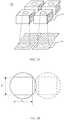
- FIG. 1A is a schematic diagram of a camera module according to some embodiments of the present disclosure.
- FIG. 1B is a schematic diagram showing a relationship between a lens imaging and an image sensing component in a camera module according to some embodiments of the present disclosure.
- FIG. 1C is a schematic diagram of a photosensitive region of an image sensing component of a camera module according to some embodiments.
- the camera module 100 includes a plurality of lenses 120, an image sensing component 160, and a plurality of optical switch components 140.
- the camera module 100 has four lenses 120, but the present disclosure is not limited thereto, and the number of the lenses 120 may be two, three, or more.
- Each lens 120 has separate components (not shown) such as a lens holder, a motor, an optical filter and so on; or all lenses 120 have common components (not shown) such as a lens holder, a motor, a filter and so on to reduce the distance between the lenses 120 and facilitate the simplified assembly and relative positioning of the plurality of lenses.
- the plurality of lenses 120 are arranged in a matrix type, but the present disclosure is not limited thereto, and the plurality of lenses may also be arranged linearly (to be described below in conjunction with FIG. 3 ). This arrangement is beneficial to reduce the distance between the lenses and facilitate the relative positioning of the plurality of lenses.
- the image sensing component 160 is disposed on the imaging side of the plurality of lenses 120.
- the area of the photosensitive region A of the image sensing component 160 is greater than the area of actual imaging region of the single lens 120 and less than the sum of the areas of actual imaging regions required by the respective lenses 120. Therefore, as shown in FIG. 1A , FIG. 1B, and FIG. 1C , the actual imaging regions C1 and C1' formed by imaging the adjacent or neighboring lenses 120 onto the image sensing component 160 overlap each other (the overlapping portions being shown by diagonal shading in the figure) to save the area of the photosensitive region of the image sensing component.
- FIG. 1B illustrates the relationship between the lens imaging and the image sensing component in detail.
- the circle C0 is the illumination region of a lens.
- the rectangle C1 is a photosensitive region corresponding to a lens 120 in the image sensing component 160, that is, the rectangle C1 is an actual imaging region of a lens.
- the area of rectangle C1 is W0 ⁇ L0.
- the circle C0' is the illumination region of the adjacent lens, and the rectangle C1' is the photosensitive region corresponding to the adjacent lens in the image sensing component 160, that is, the rectangle C1' is the actual imaging region of the adjacent lens.
- the area of the rectangle C1' is also W0 ⁇ L0.
- the actual imaging region C1' of the adjacent lens with the illumination region C0' and the actual imaging region C1 of the adjacent lens with the illumination region C0 overlap each other (as shown by the diagonal shading in the figure), the area of the overlapping region is W0 ⁇ (2L0-L1), where L1 ⁇ 2L0. That is, in the case that other conditions are the same, the area of the photosensitive region of the image sensing component can save at least the area W0 ⁇ (2L0-L1), in the camera module with two lenses according to the present disclosure.
- the four lenses 120 corresponding to the matrix arrangement of FIG. 1A both the two sides of the actual imaging region corresponding to each lens are overlapped with the actual imaging regions of the adjacent lenses from each other, respectively (as shown by the diagonal shading in the figure). That is, in the case that the other conditions are the same, the area of the photosensitive region of the image sensing component can save at least the area W1 ⁇ L1-W0 ⁇ L0, in the camera module with four lens of the present disclosure as shown in FIG. 1A , where L1 ⁇ 2L0, W1 ⁇ 2W0, and W0, W1, L0, and L1 are all positive numbers.
- an optical element that guides the light passing through the lens to reflect or refract that is, the light of the lens 120 can be directly imaged onto the image sensing component 160, and the actual imaging regions of the adjacent lenses 120 are allowed to overlap each other.
- the image sensing component 160 can be a charge coupled device (CCD) or a complementary metal oxide semiconductor (CMOS) image sensor.
- the size and shape of the image sensing component 160 can be designed and adjusted according to the number, type, and arrangement of the lenses so that the area of the photosensitive region of the image sensing component 160 is less than the sum of the areas of actual imaging regions required by each lens 120, and thus the actual imaging regions formed by imaging the adjacent lenses 120 onto the image sensing component 160 overlap each other (the overlapping portions being shown by diagonal shading in the figure), so as to save the area of the photosensitive region of the image sensing component, and achieve the effects of reducing the occupied space and saving the costs.
- the plurality of optical switch components 140 are disposed between the plurality of lenses 120 and the image sensing component 160 and are in one-to-one correspondence with the plurality of lenses 120. Each optical switch component 140 is controlled to switch between an on state and an off state, and the adjacent optical switch components corresponding to the adjacent lenses whose actual imaging regions overlap each other are not turned on at the same time.
- each lens can be equipped with a larger photosensitive area as much as possible in a common image sensing component, thereby improving the imaging quality.
- the optical switch component is an optical physical element capable of controlling whether or not the light passing through the lens is irradiated onto the image sensing component.
- the optical switch component 140 can be a controlled mechanical shutter, such as a micro-electromechanical system (MEMS) shutter, which is turned on and off after receiving a control signal from a processor (to be described below in conjunction with FIG. 8 ) to control whether or not the light passing through the lens 120 is illuminated onto the image sensing component 160.
- MEMS micro-electromechanical system
- the optical switch component 140 can also be any kind of physical shutter or optical shutter capable of receiving a control signal of the processor and controlling whether or not the light passing through the lens is irradiated onto the image sensing component.
- the actual imaging region of each lens 120 on the image sensing component 160 may overlap to some extent. If these lenses 120 are imaging at the same time, there may be a problem of mutual interference between the images. For this reason, by adding an optical switch component 140 to each lens 120, only the optical switch component 140 of the lens 120 which is called and in the working state is in the on state, and the optical switch components on the remaining lenses are all in the off state. Therefore, interference problems caused by overlapping of actual imaging regions of the plurality of lenses on the same image sensing component can be avoided.
- the camera module 100 of the present disclosure After assembling the plurality of lenses 120, the plurality of optical switch components 140, and a single image sensing component 160, it is required to perform the calibrating and demarcating operations to determine that each lens 120 can be imaged onto a predetermined actual imaging region on the image sensing component 160, and corresponding debugging is performed.
- the corresponding optical switch component 140 of the lens is turned on, and the corresponding photosensitive region on the image sensing component 160 is activated.
- a plurality of optical switch components 140 can be controlled to be sequentially turned on, in order to image on the image sensing component 160 sequentially and successively.
- a part of the plurality of optical switch components 140 (that is, the optical switch components corresponding to lenses with no overlap in the actual imaging region) is controlled to be turned on (it will be described below in conjunction with FIG. 3 ), and imaged on the image sensing component simultaneously.
- FIG. 2A is a schematic diagram of a camera module according to an example for comparison.
- FIG. 2B is a schematic diagram showing a relationship between a lens imaging and an image sensing component in a camera module according to some embodiments.
- the camera module 10 includes a plurality of lenses 12 and an image sensing component 16 in one-to-one correspondence with the plurality of lenses 12.
- the plurality of lenses 12 are arranged loosely, and the actual imaging regions of the adjacent lenses 12 on the image sensing component 16 do not overlap with each other.
- Each lens 12 and the image sensing component 16 are controlled by the electronic optical switch component to form relatively independent images without interferences between the images.
- such a camera module 10 occupies a larger internal space as a whole, thereby limiting the degree of freedom in designing the back of the mobile terminal.
- the area of the photosensitive region of the image sensing component (W ⁇ L, where W ⁇ W0, L ⁇ L0) is limited, and due to the cost considerations, the image sensing component usually used in lenses other than the main camera is generally weaker or far weaker than that of the main camera, which affects the final imaging quality.
- the area of the photosensitive region of the image sensing component is greater than the area of actual imaging region of a single lens and less than the sum of the areas of actual imaging regions of respective lenses, that is, the actual imaging regions of part of the lenses can overlap with each other, thereby allowing the lens arrangement more closely, occupying less internal space, and allowing the higher degree of freedom in designing the back of the mobile terminals that use the camera module.
- the area of the photosensitive region of the image sensing component shared by the plurality of lenses is less than the sum of the areas of actual imaging regions required by the respective lenses, thereby reducing the total photosensitive region of the image sensing component, not only saving the space occupied, but also reducing the cost.
- each lens can be equipped with a larger photosensitive area (W0 ⁇ L0>W ⁇ L) as much as possible in the common image sensing component, or a better image sensing component (for example, with a lower signal-to-noise ratio) is selected for the common image sensing component to improve imaging quality.
- FIG. 3 is a schematic diagram of a camera module according to another exemplary embodiment.
- the difference from the embodiments shown in FIG. 1A to FIG. 1C lies in that there are, in the camera module 200 of the embodiment shown in FIG. 3 , three linearly arranged lenses 220, and the area of the photosensitive area of the image sensing component 260 is greater than the actual imaging region of a single lens 220 and less than the sum of the areas of actual imaging regions of the three linearly arranged lenses 220. That is, in these embodiments, the intermediate lenses can overlap with the actual imaging regions corresponding to the adjacent lenses on both sides.
- the total area of the photosensitive region of the image sensing component is W0 ⁇ L2, where L2 ⁇ 3L0.
- the total area of the photosensitive regions of the image sensing component in the camera module according to these embodiments can save at least the area W0 ⁇ (3L0-L2).
- a plurality of optical switch components 220 can be controlled to be turned on sequentially and successively to form images on the image sensing component 260 sequentially and successively.
- a part of the plurality of optical switch components 220 (that is, the optical switch components corresponding to the lenses with no overlap in the actual imaging regions, such as the optical switch components corresponding to the two lenses at the left and right ends) is controlled to be turned on, and imaged on the image sensing component 260 simultaneously.
- FIG. 4 is a schematic diagram showing a positional relationship between a lens and an imaging plane in a camera module according to some embodiments.
- the structural schematic diagram of the camera module shown in FIG. 4 can refer to FIG. 3 accordingly, in which a plurality of lenses in the camera module are arranged linearly.
- each lens H e.g., 120, 220
- the optical axis X of each lens H is perpendicular to the plane P (that is, the photosensitive plane) where the photosensitive region of the image sensing component is located.
- the light passing through each lens H passes through the optical switch component S (e.g., 140, 240) at the shortest distance to reach the photosensitive plane P of the image sensing component.
- the diverse combination way of the lenses in the camera module can be as follows:
- the performance parameters of the plurality of lenses H are the same.
- the plurality of optical switch components S are controlled to be turned on successively, so that the light of the lens H is imaged on the photosensitive plane P of the image sensing component sequentially and successively.
- the parameters of the lenses are the same and the lenses are arranged closely (as described above), the perspective ranges of the respective lenses are highly overlapped, so that the image fusion technology can be utilized to perform the fusion operation on the overlapping regions of sequentially imaged pictures. As a result, not only a high-quality picture can be obtained, but also depth-of-field data information can be acquired.
- the plurality of lenses H adopt respectively different performance parameters, for example, different focal lengths (such as macro and telephoto), different apertures, and different viewing angles (such as wide-angle, ultra-wide-angle).
- the combination way can be, for example, a four-shot combination of an ultra-wide-angle lens, a telephoto lens, a main lens, and a blur lens; or a three-shot combination of a color lens, a black-and-white lens, and a telephoto lens; or a three-shot combination of a wide-angle lens, a telephoto lens, and a color lens; and so on.
- an optical element that guides light passing through the lens to reflect or refract that is, the light from the lens can be directly imaged onto the image sensing component, and the actual imaging regions of adjacent lenses are allowed to be overlapped with each other.
- the photosensitive region of the image sensing component can be reutilized by the camera module, so that each lens can be imaged onto the same high-quality image sensing component, thereby controlling the costs in the case of diversifying the capturing functions.
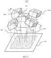
- FIG. 5 is a schematic diagram of a camera module according to still another exemplary embodiment.
- FIG. 6 is a schematic diagram showing the positional relationship between the lens and the imaging plane along the line I-I' in FIG. 5 .
- the camera module 300 includes a plurality of lenses, an image sensing component 360 and a plurality of optical switch components 340.
- the plurality of lenses of the camera module 300 includes a main lens 320 and a plurality of sub lenses 320a, 320b, 320c, and 320d. As shown in FIG.
- the optical axis X of the main lens H (320) is perpendicular to the plane P (that is, the photosensitive plane) where the image sensing component is located, and the optical axes Xa, Xb of the plurality of sub lenses Ha, Hb (320a, 320b) form an angle with the plane P where the image sensing component 360 is located, respectively.
- the light from each lens passes through the optical switch component S and reaches the photosensitive plane P of the image sensing component.
- a plurality of sub lenses 320a, 320b, 320c, and 320d are disposed around the main lens 320.
- the plurality of sub lenses 320a, 320b, 320c, and 320d are arranged to be center symmetrical with respect to the main lens 320.
- the number of sub lenses is five and the number of main lenses is one, but the present disclosure is not limited thereto, and it is possible that six sub lenses surround one main lens; alternatively, there can be two main lenses, and 6 sub lenses surround the two main lenses.
- the optical axes Xa, Xb of each of the sub lenses Ha, Hb (320a, 320b) are mirror-symmetrical with respect to the optical axis X of the main lens H (320), but it is not limited thereto.
- the main lens 320 and the respective sub-lenses 320a, 320b, 320c, and 320d are called in turn to capture the plurality of images to be synthesized later with a super wide-angle effect.
- the corresponding optical switch components are sequentially turned on in a very short time, so that each lens is imaged on a common image sensing component, and then the acquired images are synthesized, thereby achieving an ultra-wide-angle capturing effect. Therefore, the range of the angle of view FOV of the camera module of these embodiments is relatively large, and the wide-angle distortion at the edges can be better controlled.
- the same high-quality image sensing component such as with a lower signal-to-noise ratio
- the main lens is called under the ultra-wide-angle imaging effect, which can effectively improve the imaging quality.
- the main lens 320 and the respective sub-lenses 320a, 320b, 320c, and 320d can be called separately to take photos or videos at corresponding angles.
- it is selected to turning on separately an optical switch component of a sub-lens with a tilted optical axis, to enable the sub-lens to be imaged on a common image sensing component, thereby facilitating the user to achieve photos/videos with different angles without moving a mobile phone.
- the angle formed by the optical axis of the respective sub-lenses 320a, 320b, 320c, and 320d and the plane P where the image sensing component 360 is located can be adjusted.
- the sub-lenses 320a, 320b, 320c, and 320d can be tilt-shift lens. Therefore, it is easier for the user to adjust the viewing angle range of the camera module according to these embodiments.
- the optical switch component by sequentially turning on or separately turning on the optical switch component to call the sub-lens with the tilted optical axis, it can share the same high-quality image sensing component as the main lens, thereby the cost can be reduced under the premise of the same image quality or the image quality can be improved under premise of the same cost.
- FIG. 7 is a schematic diagram of a positional relationship between a lens and an imaging plane in a camera module according to yet another exemplary embodiment.
- the difference from the embodiments shown in FIG. 5 and FIG. 6 lies in that, as shown in FIG. 7 , a plurality of lenses are linearly arranged, and the optical axes of the respective sub lenses H1, H2, and H3 are at different angles to the plane P where the image sensing component is located.
- the plurality of sub lenses H1, H2, and H3 arranged linearly are located on the same side of the main lens H.
- the farther the sub-lens from the main lens H the smaller the angle with the plane P where the image sensing component is located.
- the main lens H and the respective sub-lenses H1, H2, and H3 are called in turn to form an image on a common image sensing component, and then the acquired images are synthesized, thereby achieving an ultra-wide-angle capturing effect. Therefore, the range of the angle of view FOV of the camera module of these embodiments is relatively large, and the wide-angle distortion at the edges can be better controlled. Furthermore, the same high-quality image sensing component (such as with a lower signal-to-noise ratio) as the main lens is called under the ultra-wide-angle imaging effect, which can effectively improve the imaging quality.
- the main lens H and the respective sub lenses H1, H2, and H3 can be called separately so as to take photos or videos at corresponding angles.
- it is selected to turn on separately the optical switch component of a sub-lens with the largest tilt of optical axis, so that the sub-lens is imaged on a common image sensing component, thereby facilitating the user to achieve photos/videos with a special angle (such as top or bottom capturing) without moving a mobile phone.
- a special angle such as top or bottom capturing
- each of the sub-lenses H1, H2, and H3 can be a tilt-shift lens. Therefore, it is easier for the user to adjust the viewing angle range of the camera module according to these embodiments as needed.
- the optical switch component by sequentially turning on or separately turning on the optical switch component to call the sub-lens with the tilted optical axis, it can share the same high-quality image sensing component as the main lens, thereby the cost can be reduced under the premise of the same image quality or the image quality can be improved under premise of the same cost.
- FIG. 8 is a block diagram showing a mobile terminal 800 according to some embodiments.
- the mobile terminal 800 is, for example, a smartphone, a tablet, or the like.
- the mobile terminal 800 can include one or more of the following components: a processing component 802, a memory 804, a power component 806, a multimedia component 808, an audio component 810, an input/output (I/O) interface 812, a sensor component 814, and a communication component 816.
- a processing component 802 a memory 804
- a power component 806 a multimedia component 808, an audio component 810, an input/output (I/O) interface 812, a sensor component 814, and a communication component 816.
- I/O input/output
- the processing component 802 typically controls overall operations of the mobile terminal 800, such as the operations associated with display, telephone calls, data communications, camera operations, and recording operations.
- the processing component 802 can include one or more processors 820 to execute instructions to perform all or part of the steps in the above described methods.
- the processor 820 controls a plurality of optical switch components of the camera module to switch between a turning on state and a turning off state, and adjacent optical switch components corresponding to adjacent lenses whose actual imaging areas overlap each other are not turned on at the same time.
- the processor 820 may control one of the optical switch components to be turned on to perform required capturing according to the input selection signal; or the processor 820 may control to sequentially turn on the optical switch components to take pictures, and retrieve the sequentially captured images for synthesis.
- the processing component 802 can include one or more modules which facilitate the interaction between the processing component 802 and other components.
- the processing component 802 can include a multimedia module to facilitate the interaction between the multimedia component 808 and the processing component 802.
- the memory 804 is configured to store various types of data to support the operation of the mobile terminal 800. Examples of such data include instructions for any applications or methods operated on the mobile terminal 800, contact data, phonebook data, messages, pictures, video, etc.
- the memory 804 can be implemented using any type of volatile or non-volatile memory devices, or a combination thereof, such as a static random access memory (SRAM), an electrically erasable programmable read-only memory (EEPROM), an erasable programmable read-only memory (EPROM), a programmable read-only memory (PROM), a read-only memory (ROM), a magnetic memory, a flash memory, a magnetic or optical disk.
- SRAM static random access memory
- EEPROM electrically erasable programmable read-only memory
- EPROM erasable programmable read-only memory
- PROM programmable read-only memory
- ROM read-only memory
- magnetic memory a magnetic memory
- flash memory a flash memory
- magnetic or optical disk a magnetic
- the power component 806 provides power to various components of the mobile terminal 800.
- the power component 806 can include a power management system, one or more power sources, and any other components associated with the generation, management, and distribution of power in the mobile terminal 800.
- the multimedia component 808 includes a screen providing an output interface between the mobile terminal 800 and the user.
- the screen can include a liquid crystal display (LCD) and a touch panel (TP).
- LCD liquid crystal display
- TP touch panel
- OLED organic light-emitting diode
- the screen can be implemented as a touch screen to receive input signals from the user.
- the touch panel includes one or more touch sensors to sense touches, swipes, and gestures on the touch panel.
- the touch sensors not only can sense a boundary of a touch or swipe action, but also can sense a period of time and a pressure associated with the touch or swipe action.
- the multimedia component 808 includes a front camera and/or a rear camera.
- the front camera and the rear camera can receive an external multimedia datum while the mobile terminal 800 is in an operation mode, such as a photographing mode or a video mode.
- Each of the front camera and the rear camera can be a fixed optical lens system or have focus and optical zoom capability.
- the audio component 810 is configured to output and/or input audio signals.
- the audio component 810 includes a microphone ("MIC") configured to receive an external audio signal when the mobile terminal 800 is in an operation mode, such as a call mode, a recording mode, and a voice recognition mode.
- the received audio signal can be further stored in the memory 804 or transmitted via the communication component 816.
- the audio component 810 further includes a speaker to output audio signals.
- the I/O interface 812 provides an interface between the processing component 802 and peripheral interface modules, such as a keyboard, a click wheel, buttons, and the like.
- the buttons can include, but are not limited to, a home button, a volume button, a starting button, and a locking button.
- the sensor component 814 includes one or more sensors to provide status assessments of various aspects of the mobile terminal 800. For instance, the sensor component 814 can detect an open/closed status of the mobile terminal 800, relative positioning of components such as the display and the keypad, of the mobile terminal 800, a change in position of the mobile terminal 800 or a component of the mobile terminal 800, a presence or absence of user contact with the mobile terminal 800, an orientation or an acceleration/deceleration of the mobile terminal 800, and a change in temperature of the mobile terminal 800.
- the sensor component 814 can include a proximity sensor configured to detect the presence of nearby objects without any physical contact.
- the sensor component 814 includes a light sensor, such as a CMOS or CCD image sensor, for use in imaging applications.
- the sensor component 814 can also include an accelerometer sensor, a gyroscope sensor, a magnetic sensor, a pressure sensor, or a temperature sensor.
- the communication component 816 is configured to facilitate wired or wireless communication between the mobile terminal 800 and other devices.
- the mobile terminal 800 can access a wireless network based on a communication standard, such as Wi-Fi, 2G, 3G, 4G, 5G, or a combination thereof.
- the communication component 816 receives a broadcast signal or broadcast associated information from an external broadcast management system via a broadcast channel.
- the communication component 816 further includes a near field communication (NFC) module to facilitate short-range communications.
- the NFC module can be implemented based on a radio frequency identification (RFID) technology, an infrared data association (IrDA) technology, an ultra-wideband (UWB) technology, a Bluetooth (BT) technology, and other technologies.
- RFID radio frequency identification
- IrDA infrared data association
- UWB ultra-wideband
- BT Bluetooth
- the mobile terminal 800 can be implemented with one or more application specific integrated circuits (ASICs), digital signal processors (DSPs), digital signal processing devices (DSPDs), programmable logic devices (PLDs), field programmable gate arrays (FPGAs), controllers, micro-controllers, microprocessors, or other electronic components, for performing the above described methods.
- ASICs application specific integrated circuits
- DSPs digital signal processors
- DSPDs digital signal processing devices
- PLDs programmable logic devices
- FPGAs field programmable gate arrays
- controllers micro-controllers, microprocessors, or other electronic components, for performing the above described methods.
- non-transitory computer-readable storage medium including instructions, such as included in the memory 804, executable by the processor 820 in the mobile terminal 800, for performing the above-described methods.
- the non-transitory computer-readable storage medium can be a ROM, a RAM, a CD-ROM, a magnetic tape, a floppy disc, an optical data storage device, and the like.
- the area of the photosensitive region of the image sensing component can be greater than the area of actual imaging region of a single lens and less than the sum of the areas of actual imaging regions of respective lenses, that is, the actual imaging regions of part of the lenses can overlap each other, thereby enabling the arrangement of the lens more compact, occupying less internal space, and allowing a higher degree of freedom in designing the back of mobile terminals using the camera module.
- the area of the photosensitive region of the image sensing component shared by the plurality of lenses can be less than the sum of the areas of the actual imaging regions required by each of the lenses, thereby reducing the total photosensitive region of the image sensing component, which not only saves space occupied but also reduces costs.
- each lens can be equipped with a larger sensing area in the common image sensing component as much as possible, or a higher-quality image sensing component can be selected for the common image sensing component, thereby improving imaging quality.
- each lens can be called separately to capture photos or videos at corresponding angles.
- the optical switch component of a sub-lens with a tilted optical axis can be turned on separately, so that the sub-lens can be imaged on a common image sensing component, and thus the user can achieve photos/videos with a special angle (such as a top or bottom capturing) without moving the mobile phone.
- a special angle such as a top or bottom capturing
- the main lens and each sub-lens are called in turn, imaging on a common image sensing component, and then synthesizing the acquired images to obtain an ultra-wide-angle capturing effect. Therefore, the range of the angle of view FOV of the camera module of these embodiments is made relatively large, and the wide-angle distortion at the edges can be better controlled.
- the optical switch component By sequentially turning on or separately turning on the optical switch component to call the sub-lens with tilted optical axis, it can be shared with the high-quality image sensing component like the main lens, so as to achieving the reduction of the cost under the premise of the same image quality or the improvement of the image quality under the premise of the same cost.
- control and/or interface software or app can be provided in a form of a non-transitory computer-readable storage medium having instructions stored thereon is further provided.
- the non-transitory computer-readable storage medium can be a ROM, a CD-ROM, a magnetic tape, a floppy disk, optical data storage equipment, a flash drive such as a USB drive or an SD card, and the like.
- Implementations of the subject matter and the operations described in this disclosure can be implemented in digital electronic circuitry, or in computer software, firmware, or hardware, including the structures disclosed herein and their structural equivalents, or in combinations of one or more of them. Implementations of the subject matter described in this disclosure can be implemented as one or more computer programs, i.e., one or more portions of computer program instructions, encoded on one or more computer storage medium for execution by, or to control the operation of, data processing apparatus.
- the program instructions can be encoded on an artificially-generated propagated signal, e.g., a machine-generated electrical, optical, or electromagnetic signal, which is generated to encode information for transmission to suitable receiver apparatus for execution by a data processing apparatus.
- an artificially-generated propagated signal e.g., a machine-generated electrical, optical, or electromagnetic signal, which is generated to encode information for transmission to suitable receiver apparatus for execution by a data processing apparatus.
- a computer storage medium can be, or be included in, a computer-readable storage device, a computer-readable storage substrate, a random or serial access memory array or device, or a combination of one or more of them.
- a computer storage medium is not a propagated signal
- a computer storage medium can be a source or destination of computer program instructions encoded in an artificially-generated propagated signal.
- the computer storage medium can also be, or be included in, one or more separate components or media (e.g., multiple CDs, disks, drives, or other storage devices). Accordingly, the computer storage medium can be tangible.
- the operations described in this disclosure can be implemented as operations performed by a data processing apparatus on data stored on one or more computer-readable storage devices or received from other sources.
- the devices in this disclosure can include special purpose logic circuitry, e.g., an FPGA (field-programmable gate array), or an ASIC (application-specific integrated circuit).
- the device can also include, in addition to hardware, code that creates an execution environment for the computer program in question, e.g., code that constitutes processor firmware, a protocol stack, a database management system, an operating system, a cross-platform runtime environment, a virtual machine, or a combination of one or more of them.
- the devices and execution environment can realize various different computing model infrastructures, such as web services, distributed computing, and grid computing infrastructures.
- a computer program (also known as a program, software, software application, app, script, or code) can be written in any form of programming language, including compiled or interpreted languages, declarative or procedural languages, and it can be deployed in any form, including as a stand-alone program or as a portion, component, subroutine, object, or other portion suitable for use in a computing environment.
- a computer program can, but need not, correspond to a file in a file system.
- a program can be stored in a portion of a file that holds other programs or data (e.g., one or more scripts stored in a markup language document), in a single file dedicated to the program in question, or in multiple coordinated files (e.g., files that store one or more portions, sub-programs, or portions of code).
- a computer program can be deployed to be executed on one computer or on multiple computers that are located at one site or distributed across multiple sites and interconnected by a communication network.
- the processes and logic flows described in this disclosure can be performed by one or more programmable processors executing one or more computer programs to perform actions by operating on input data and generating output.
- the processes and logic flows can also be performed by, and apparatus can also be implemented as, special purpose logic circuitry, e.g., an FPGA, or an ASIC.
- processors or processing circuits suitable for the execution of a computer program include, by way of example, both general and special purpose microprocessors, and any one or more processors of any kind of digital computer.
- a processor will receive instructions and data from a read-only memory, or a random-access memory, or both.
- Elements of a computer can include a processor configured to perform actions in accordance with instructions and one or more memory devices for storing instructions and data.
- a computer will also include, or be operatively coupled to receive data from or transfer data to, or both, one or more mass storage devices for storing data, e.g., magnetic, magneto-optical disks, or optical disks.
- mass storage devices for storing data
- a computer need not have such devices.
- a computer can be embedded in another device, e.g., a mobile telephone, a personal digital assistant (PDA), a mobile audio or video player, a game console, a Global Positioning System (GPS) receiver, or a portable storage device (e.g., a universal serial bus (USB) flash drive), to name just a few.
- PDA personal digital assistant
- GPS Global Positioning System
- USB universal serial bus
- Devices suitable for storing computer program instructions and data include all forms of non-volatile memory, media and memory devices, including by way of example semiconductor memory devices, e.g., EPROM, EEPROM, and flash memory devices; magnetic disks, e.g., internal hard disks or removable disks; magneto-optical disks; and CD-ROM and DVD-ROM disks.
- semiconductor memory devices e.g., EPROM, EEPROM, and flash memory devices
- magnetic disks e.g., internal hard disks or removable disks
- magneto-optical disks e.g., CD-ROM and DVD-ROM disks.
- the processor and the memory can be supplemented by, or incorporated in, special purpose logic circuitry.
- implementations of the subject matter described in this specification can be implemented with a computer and/or a display device, e.g., a VR/AR device, a head-mount display (HMD) device, a head-up display (HUD) device, smart eyewear (e.g., glasses), a CRT (cathode-ray tube), LCD (liquid-crystal display), OLED (organic light emitting diode), or any other monitor for displaying information to the user and a keyboard, a pointing device, e.g., a mouse, trackball, etc., or a touch screen, touch pad, etc., by which the user can provide input to the computer.
- a display device e.g., a VR/AR device, a head-mount display (HMD) device, a head-up display (HUD) device, smart eyewear (e.g., glasses), a CRT (cathode-ray tube), LCD (liquid-crystal display), OLED (organic light emitting dio
- Implementations of the subject matter described in this specification can be implemented in a computing system that includes a back-end component, e.g., as a data server, or that includes a middleware component, e.g., an application server, or that includes a front-end component, e.g., a client computer having a graphical user interface or a Web browser through which a user can interact with an implementation of the subject matter described in this specification, or any combination of one or more such back-end, middleware, or front-end components.
- a back-end component e.g., as a data server
- a middleware component e.g., an application server
- a front-end component e.g., a client computer having a graphical user interface or a Web browser through which a user can interact with an implementation of the subject matter described in this specification, or any combination of one or more such back-end, middleware, or front-end components.
- the components of the system can be interconnected by any form or medium of digital data communication, e.g., a communication network.
- communication networks include a local area network ("LAN”) and a wide area network (“WAN”), an inter-network (e.g., the Internet), and peer-to-peer networks (e.g., ad hoc peer-to-peer networks).
- LAN local area network
- WAN wide area network
- Internet inter-network
- peer-to-peer networks e.g., ad hoc peer-to-peer networks.
Landscapes
- Engineering & Computer Science (AREA)
- Multimedia (AREA)
- Signal Processing (AREA)
- Physics & Mathematics (AREA)
- General Physics & Mathematics (AREA)
- Computing Systems (AREA)
- Theoretical Computer Science (AREA)
- Cameras In General (AREA)
- Studio Devices (AREA)
Abstract
Description
- In order to improve the captured picture quality or obtain diversified capturing effects, current mobile terminals (such as mobile phones or tablet computers, etc.) are generally equipped with a plurality of cameras, such as two, three, four or even a dozen cameras. In the camera modules of these mobile terminals, a form of an image sensing component, such as a complementary metal-oxide-semiconductor (CMOS) image sensor, and a lens, is employed. Generally, a mobile terminal may need as many sets of lenses and image sensing components as the number of cameras it possesses, so that a user can select a variety of different cameras to achieve the desired capturing effect.
- However, a plurality of camera modules may occupy a larger space in the body of a mobile terminal. Moreover, due to cost considerations, the qualities of the image sensing components selected in different camera modules are different, and usually only the main lens is equipped with a high-quality image sensing component, which results in that photo/video quality of the mobile terminal has large variations.
- In addition, in order to obtain a larger capturing angle, the mobile terminals usually need to separately add a set of ultra-wide-angle lenses and image sensing components. However, such a single set of ultra-wide-angle camera modules is usually difficult to achieve both quality and cost. Moreover, since ultra-wide-angle lenses usually have wide-angle distortion, it is difficult to make the camera field of view (FOV) of a general mobile terminal very large to prevent the distortion at the edges from being too heavy and seriously affecting the imaging effect.
- The present disclosure relates generally to the technical field of mobile terminals, and more specifically to a camera module, and a mobile terminal having the camera module.
- The camera module and the mobile terminal having the camera module according to various embodiments of the present disclosure can effectively reduce the total space occupied by the camera, reduce cost of the mobile terminal, and improve imaging quality.
- According to a first aspect of the present disclosure, there is provided a camera module, including:
- a plurality of lenses;
- an image sensing component, disposed on an imaging side of the plurality of lenses, and an area of a photosensitive region of the image sensing component being greater than an area of actual imaging region of a single lens and less than the sum of the area of actual imaging region of each of the lenses; and
- a plurality of optical switch components, disposed, between the plurality of lenses and the image sensing component, corresponding to the plurality of lenses;
- wherein the optical switch component is controlled to switch between an on state and an off state, and neighboring optical switch components corresponding to neighboring lenses whose actual imaging regions overlap each other are not turned on at the same time.
- Preferably, at least two or more lenses of the plurality of lenses are arranged linearly. Therein, in particular, the optical switch component is arranged between the at least two or more lenses and the image sensing component.
- Preferably, at least two or more of the plurality of lenses are arranged in a matrix. In particular, all lenses of the plurality of lenses are arranged in a matrix. Therein, in particular, the optical switch component is arranged between each of the least two or more lenses and the image sensing component.
- Preferably, the neighboring lenses are directly imaged onto the image sensing component, and the actual imaging regions of the neighboring lenses are overlapped with each other.
- Preferably, in an image capturing operation, the plurality of optical switch components are controlled to be turned on sequentially and successively so as to be imaged sequentially and successively on the image sensing component.
- Preferably, in an image capturing operation, the optical switch component corresponding to the lens with no overlap in the actual imaging region is controlled to be turned on so as to be imaged simultaneously on the image sensing component.
- Preferably, the image sensing component is one of a charge-coupled image sensor and a metal oxide semiconductor image sensor.
- Preferably, the optical switch component is a micro-electromechanical system (MEMS) shutter.
- According to a second aspect of the present disclosure, a mobile terminal is provided. The mobile terminal includes: any one of the camera modules described above; and a processor that controls the plurality of optical switch components to switch between an on state and an off state, and neighboring optical switch components corresponding to neighboring lenses whose actual imaging regions overlap each other are not turned on at the same time.
- Preferably, a front camera and/or a rear camera of the mobile terminal can be part of the camera module, or include the camera module.
- It is to be understood that both the foregoing general description and the following detailed description are exemplary and explanatory only and are not restrictive of the disclosure.
- The accompanying drawings, which are incorporated in and constitute a part of this description, illustrate embodiments consistent with the disclosure and, together with the description, serve to explain the principles of the disclosure.
-
FIG. 1A is a schematic diagram of a camera module according to some embodiments of the present disclosure. -
FIG. 1B is a schematic diagram showing a relationship between a lens imaging and an image sensing component in a camera module according to some embodiments of the present disclosure. -
FIG. 1C is a schematic diagram of a photosensitive region of an image sensing component of a camera module according to some embodiments. -
FIG. 2A is a schematic diagram of a camera module according to an example for comparison. -
FIG. 2B is a schematic diagram showing a relationship between lens imaging and an image sensing component in a camera module according to some embodiments. -
FIG. 3 is a schematic diagram of a camera module according to another exemplary embodiment. -
FIG. 4 is a schematic diagram showing a positional relationship between a lens and an imaging plane in a camera module according to some embodiments. -
FIG. 5 is a schematic diagram of a camera module according to still another exemplary embodiment. -
FIG. 6 is a schematic diagram showing the positional relationship between the lens and the imaging plane along the line I-I' inFIG. 5 . -
FIG. 7 is a schematic diagram of a positional relationship between a lens and an imaging plane in a camera module according to still another exemplary embodiment. -
FIG. 8 is a block diagram showing a mobile terminal according to some embodiments. - Description will now be made herein in detail to exemplary embodiments, examples of which are illustrated in the accompanying drawings. The following description refers to the accompanying drawings in which the same numbers in different drawings represent the same or similar elements unless otherwise represented. The implementations set forth in the following description of exemplary embodiments do not represent all implementations consistent with the disclosure. In contrast, they are merely examples of devices and methods consistent with some aspects related to the disclosure as recited in the appended claims.
-
FIG. 1A is a schematic diagram of a camera module according to some embodiments of the present disclosure.FIG. 1B is a schematic diagram showing a relationship between a lens imaging and an image sensing component in a camera module according to some embodiments of the present disclosure.FIG. 1C is a schematic diagram of a photosensitive region of an image sensing component of a camera module according to some embodiments. - As shown in
FIG. 1A , thecamera module 100 includes a plurality oflenses 120, animage sensing component 160, and a plurality ofoptical switch components 140. InFIG. 1A , thecamera module 100 has fourlenses 120, but the present disclosure is not limited thereto, and the number of thelenses 120 may be two, three, or more. Eachlens 120 has separate components (not shown) such as a lens holder, a motor, an optical filter and so on; or alllenses 120 have common components (not shown) such as a lens holder, a motor, a filter and so on to reduce the distance between thelenses 120 and facilitate the simplified assembly and relative positioning of the plurality of lenses. - In
FIG. 1A , the plurality oflenses 120 are arranged in a matrix type, but the present disclosure is not limited thereto, and the plurality of lenses may also be arranged linearly (to be described below in conjunction withFIG. 3 ). This arrangement is beneficial to reduce the distance between the lenses and facilitate the relative positioning of the plurality of lenses. - The
image sensing component 160 is disposed on the imaging side of the plurality oflenses 120. The area of the photosensitive region A of theimage sensing component 160 is greater than the area of actual imaging region of thesingle lens 120 and less than the sum of the areas of actual imaging regions required by therespective lenses 120. Therefore, as shown inFIG. 1A ,FIG. 1B, and FIG. 1C , the actual imaging regions C1 and C1' formed by imaging the adjacent or neighboringlenses 120 onto theimage sensing component 160 overlap each other (the overlapping portions being shown by diagonal shading in the figure) to save the area of the photosensitive region of the image sensing component. -
FIG. 1B illustrates the relationship between the lens imaging and the image sensing component in detail. The circle C0 is the illumination region of a lens. The rectangle C1 is a photosensitive region corresponding to alens 120 in theimage sensing component 160, that is, the rectangle C1 is an actual imaging region of a lens. The area of rectangle C1 is W0∗L0. The circle C0' is the illumination region of the adjacent lens, and the rectangle C1' is the photosensitive region corresponding to the adjacent lens in theimage sensing component 160, that is, the rectangle C1' is the actual imaging region of the adjacent lens. The area of the rectangle C1' is also W0∗L0. In order to achieve the effect of saving the image sensing component, the actual imaging region C1' of the adjacent lens with the illumination region C0' and the actual imaging region C1 of the adjacent lens with the illumination region C0 overlap each other (as shown by the diagonal shading in the figure), the area of the overlapping region is W0∗(2L0-L1), where L1 < 2L0. That is, in the case that other conditions are the same, the area of the photosensitive region of the image sensing component can save at least the area W0∗(2L0-L1), in the camera module with two lenses according to the present disclosure. - Based on the above description in conjunction with
FIG. 1B , it can be understood that, as shown inFIG. 1C , the fourlenses 120 corresponding to the matrix arrangement ofFIG. 1A , both the two sides of the actual imaging region corresponding to each lens are overlapped with the actual imaging regions of the adjacent lenses from each other, respectively (as shown by the diagonal shading in the figure). That is, in the case that the other conditions are the same, the area of the photosensitive region of the image sensing component can save at least the area W1∗L1-W0∗L0, in the camera module with four lens of the present disclosure as shown inFIG. 1A , where L1 < 2L0, W1 < 2W0, and W0, W1, L0, and L1 are all positive numbers. - In these embodiments, there may not be provided, between the plurality of
lenses 120 and theimage sensing component 160, an optical element that guides the light passing through the lens to reflect or refract, that is, the light of thelens 120 can be directly imaged onto theimage sensing component 160, and the actual imaging regions of theadjacent lenses 120 are allowed to overlap each other. - The
image sensing component 160 can be a charge coupled device (CCD) or a complementary metal oxide semiconductor (CMOS) image sensor. The size and shape of theimage sensing component 160 can be designed and adjusted according to the number, type, and arrangement of the lenses so that the area of the photosensitive region of theimage sensing component 160 is less than the sum of the areas of actual imaging regions required by eachlens 120, and thus the actual imaging regions formed by imaging theadjacent lenses 120 onto theimage sensing component 160 overlap each other (the overlapping portions being shown by diagonal shading in the figure), so as to save the area of the photosensitive region of the image sensing component, and achieve the effects of reducing the occupied space and saving the costs. - The plurality of
optical switch components 140 are disposed between the plurality oflenses 120 and theimage sensing component 160 and are in one-to-one correspondence with the plurality oflenses 120. Eachoptical switch component 140 is controlled to switch between an on state and an off state, and the adjacent optical switch components corresponding to the adjacent lenses whose actual imaging regions overlap each other are not turned on at the same time. - As shown in
FIG. 1A , the actual imaging regions of the fourlenses 120 arranged closely in a matrix are all overlapped, and when one of the fourlenses 120 is in the on state, the remaining optical switch components are in the off state, so that only the lens corresponding to the turned-on optical switch component is imaged on the photosensitive region of the image sensing component. Therefore, each lens can be equipped with a larger photosensitive area as much as possible in a common image sensing component, thereby improving the imaging quality. - In the present disclosure, the optical switch component is an optical physical element capable of controlling whether or not the light passing through the lens is irradiated onto the image sensing component. The
optical switch component 140 can be a controlled mechanical shutter, such as a micro-electromechanical system (MEMS) shutter, which is turned on and off after receiving a control signal from a processor (to be described below in conjunction withFIG. 8 ) to control whether or not the light passing through thelens 120 is illuminated onto theimage sensing component 160. Theoptical switch component 140 can also be any kind of physical shutter or optical shutter capable of receiving a control signal of the processor and controlling whether or not the light passing through the lens is irradiated onto the image sensing component. - In the above-mentioned embodiments of the present disclosure, since the plurality of
lenses 120 and theimage sensing component 160 are arranged in the foregoing manner, the actual imaging region of eachlens 120 on theimage sensing component 160 may overlap to some extent. If theselenses 120 are imaging at the same time, there may be a problem of mutual interference between the images. For this reason, by adding anoptical switch component 140 to eachlens 120, only theoptical switch component 140 of thelens 120 which is called and in the working state is in the on state, and the optical switch components on the remaining lenses are all in the off state. Therefore, interference problems caused by overlapping of actual imaging regions of the plurality of lenses on the same image sensing component can be avoided. - For the
camera module 100 of the present disclosure, after assembling the plurality oflenses 120, the plurality ofoptical switch components 140, and a singleimage sensing component 160, it is required to perform the calibrating and demarcating operations to determine that eachlens 120 can be imaged onto a predetermined actual imaging region on theimage sensing component 160, and corresponding debugging is performed. When thecamera module 100 of the present disclosure is in use and it is desired to call alens 120, the correspondingoptical switch component 140 of the lens is turned on, and the corresponding photosensitive region on theimage sensing component 160 is activated. In an image capturing operation by the user, a plurality ofoptical switch components 140 can be controlled to be sequentially turned on, in order to image on theimage sensing component 160 sequentially and successively. Alternatively, during an image capturing operation, a part of the plurality of optical switch components 140 (that is, the optical switch components corresponding to lenses with no overlap in the actual imaging region) is controlled to be turned on (it will be described below in conjunction withFIG. 3 ), and imaged on the image sensing component simultaneously. -
FIG. 2A is a schematic diagram of a camera module according to an example for comparison.FIG. 2B is a schematic diagram showing a relationship between a lens imaging and an image sensing component in a camera module according to some embodiments. As shown inFIGS. 2A and 2B , thecamera module 10 includes a plurality oflenses 12 and animage sensing component 16 in one-to-one correspondence with the plurality oflenses 12. The plurality oflenses 12 are arranged loosely, and the actual imaging regions of theadjacent lenses 12 on theimage sensing component 16 do not overlap with each other. Eachlens 12 and theimage sensing component 16 are controlled by the electronic optical switch component to form relatively independent images without interferences between the images. However, such acamera module 10 occupies a larger internal space as a whole, thereby limiting the degree of freedom in designing the back of the mobile terminal. In addition, the area of the photosensitive region of the image sensing component (W∗L, where W < W0, L < L0) is limited, and due to the cost considerations, the image sensing component usually used in lenses other than the main camera is generally weaker or far weaker than that of the main camera, which affects the final imaging quality. - It can be seen that, in the camera module of these embodiments, because the area of the photosensitive region of the image sensing component is greater than the area of actual imaging region of a single lens and less than the sum of the areas of actual imaging regions of respective lenses, that is, the actual imaging regions of part of the lenses can overlap with each other, thereby allowing the lens arrangement more closely, occupying less internal space, and allowing the higher degree of freedom in designing the back of the mobile terminals that use the camera module. Secondly, the area of the photosensitive region of the image sensing component shared by the plurality of lenses is less than the sum of the areas of actual imaging regions required by the respective lenses, thereby reducing the total photosensitive region of the image sensing component, not only saving the space occupied, but also reducing the cost. In addition, each lens can be equipped with a larger photosensitive area (W0∗L0>W∗L) as much as possible in the common image sensing component, or a better image sensing component (for example, with a lower signal-to-noise ratio) is selected for the common image sensing component to improve imaging quality.
-
FIG. 3 is a schematic diagram of a camera module according to another exemplary embodiment. The difference from the embodiments shown inFIG. 1A to FIG. 1C lies in that there are, in thecamera module 200 of the embodiment shown inFIG. 3 , three linearly arrangedlenses 220, and the area of the photosensitive area of theimage sensing component 260 is greater than the actual imaging region of asingle lens 220 and less than the sum of the areas of actual imaging regions of the three linearly arrangedlenses 220. That is, in these embodiments, the intermediate lenses can overlap with the actual imaging regions corresponding to the adjacent lenses on both sides. The total area of the photosensitive region of the image sensing component is W0∗L2, where L2 < 3L0. In the case that the other conditions are the same, as compared with the solution that one lens is equipped with one image sensing component, the total area of the photosensitive regions of the image sensing component in the camera module according to these embodiments can save at least the area W0∗(3L0-L2). - In an image capturing operation by the user, a plurality of
optical switch components 220 can be controlled to be turned on sequentially and successively to form images on theimage sensing component 260 sequentially and successively. Alternatively, in an image capturing operation, a part of the plurality of optical switch components 220 (that is, the optical switch components corresponding to the lenses with no overlap in the actual imaging regions, such as the optical switch components corresponding to the two lenses at the left and right ends) is controlled to be turned on, and imaged on theimage sensing component 260 simultaneously. -
FIG. 4 is a schematic diagram showing a positional relationship between a lens and an imaging plane in a camera module according to some embodiments. The structural schematic diagram of the camera module shown inFIG. 4 can refer toFIG. 3 accordingly, in which a plurality of lenses in the camera module are arranged linearly. - As shown in
FIG. 4 , in the camera module, the optical axis X of each lens H (e.g., 120, 220) is perpendicular to the plane P (that is, the photosensitive plane) where the photosensitive region of the image sensing component is located. The light passing through each lens H passes through the optical switch component S (e.g., 140, 240) at the shortest distance to reach the photosensitive plane P of the image sensing component. - In the embodiment shown in
FIG. 4 , in order to achieve different capturing (photo/video) effects, the diverse combination way of the lenses in the camera module can be as follows: - The performance parameters of the plurality of lenses H are the same. In an image capturing operation, the plurality of optical switch components S are controlled to be turned on successively, so that the light of the lens H is imaged on the photosensitive plane P of the image sensing component sequentially and successively.
- In these embodiments, since the parameters of the lenses are the same and the lenses are arranged closely (as described above), the perspective ranges of the respective lenses are highly overlapped, so that the image fusion technology can be utilized to perform the fusion operation on the overlapping regions of sequentially imaged pictures. As a result, not only a high-quality picture can be obtained, but also depth-of-field data information can be acquired.
- The plurality of lenses H adopt respectively different performance parameters, for example, different focal lengths (such as macro and telephoto), different apertures, and different viewing angles (such as wide-angle, ultra-wide-angle). The combination way can be, for example, a four-shot combination of an ultra-wide-angle lens, a telephoto lens, a main lens, and a blur lens; or a three-shot combination of a color lens, a black-and-white lens, and a telephoto lens; or a three-shot combination of a wide-angle lens, a telephoto lens, and a color lens; and so on.
- In these embodiments, there may not be provided between the lens and the image sensing component, an optical element that guides light passing through the lens to reflect or refract, that is, the light from the lens can be directly imaged onto the image sensing component, and the actual imaging regions of adjacent lenses are allowed to be overlapped with each other.
- In these embodiments, since the actual imaging regions, which are formed by the adjacent lenses imaged directly onto the image sensing component, overlap with each other (as described above), the photosensitive region of the image sensing component can be reutilized by the camera module, so that each lens can be imaged onto the same high-quality image sensing component, thereby controlling the costs in the case of diversifying the capturing functions.
-
FIG. 5 is a schematic diagram of a camera module according to still another exemplary embodiment.FIG. 6 is a schematic diagram showing the positional relationship between the lens and the imaging plane along the line I-I' inFIG. 5 . As shown inFIG. 5 , thecamera module 300 includes a plurality of lenses, animage sensing component 360 and a plurality ofoptical switch components 340. The plurality of lenses of thecamera module 300 includes amain lens 320 and a plurality ofsub lenses FIG. 6 , the optical axis X of the main lens H (320) is perpendicular to the plane P (that is, the photosensitive plane) where the image sensing component is located, and the optical axes Xa, Xb of the plurality of sub lenses Ha, Hb (320a, 320b) form an angle with the plane P where theimage sensing component 360 is located, respectively. The light from each lens passes through the optical switch component S and reaches the photosensitive plane P of the image sensing component. - In these embodiments, a plurality of
sub lenses main lens 320. The plurality ofsub lenses main lens 320. In the embodiment shown inFIG. 5 , the number of sub lenses is five and the number of main lenses is one, but the present disclosure is not limited thereto, and it is possible that six sub lenses surround one main lens; alternatively, there can be two main lenses, and 6 sub lenses surround the two main lenses. - In these embodiments, as shown in
FIG. 6 , the optical axes Xa, Xb of each of the sub lenses Ha, Hb (320a, 320b) are mirror-symmetrical with respect to the optical axis X of the main lens H (320), but it is not limited thereto. - In an image capturing operation by the user, the
main lens 320 and the respective sub-lenses 320a, 320b, 320c, and 320d are called in turn to capture the plurality of images to be synthesized later with a super wide-angle effect. For example, the corresponding optical switch components are sequentially turned on in a very short time, so that each lens is imaged on a common image sensing component, and then the acquired images are synthesized, thereby achieving an ultra-wide-angle capturing effect. Therefore, the range of the angle of view FOV of the camera module of these embodiments is relatively large, and the wide-angle distortion at the edges can be better controlled. In addition, the same high-quality image sensing component (such as with a lower signal-to-noise ratio) as the main lens is called under the ultra-wide-angle imaging effect, which can effectively improve the imaging quality. - Optionally, in an image capturing operation by the user, the
main lens 320 and the respective sub-lenses 320a, 320b, 320c, and 320d can be called separately to take photos or videos at corresponding angles. For example, among the five lenses of these embodiments, it is selected to turning on separately an optical switch component of a sub-lens with a tilted optical axis, to enable the sub-lens to be imaged on a common image sensing component, thereby facilitating the user to achieve photos/videos with different angles without moving a mobile phone. In particular, in some capturing scenes where it is not convenient to place the mobile phone at a specific angle, it is possible to capture the content that cannot be taken by existing ordinary mobile phones without moving the mobile phone. - In an embodiment, the angle formed by the optical axis of the respective sub-lenses 320a, 320b, 320c, and 320d and the plane P where the
image sensing component 360 is located can be adjusted. The sub-lenses 320a, 320b, 320c, and 320d can be tilt-shift lens. Therefore, it is easier for the user to adjust the viewing angle range of the camera module according to these embodiments. - In the camera module of these embodiments, by sequentially turning on or separately turning on the optical switch component to call the sub-lens with the tilted optical axis, it can share the same high-quality image sensing component as the main lens, thereby the cost can be reduced under the premise of the same image quality or the image quality can be improved under premise of the same cost.
-
FIG. 7 is a schematic diagram of a positional relationship between a lens and an imaging plane in a camera module according to yet another exemplary embodiment. The difference from the embodiments shown inFIG. 5 andFIG. 6 lies in that, as shown inFIG. 7 , a plurality of lenses are linearly arranged, and the optical axes of the respective sub lenses H1, H2, and H3 are at different angles to the plane P where the image sensing component is located. - In the embodiment of
FIG. 7 , the plurality of sub lenses H1, H2, and H3 arranged linearly are located on the same side of the main lens H. In addition, the farther the sub-lens from the main lens H, the smaller the angle with the plane P where the image sensing component is located. - In an image capturing operation by the user, the main lens H and the respective sub-lenses H1, H2, and H3 are called in turn to form an image on a common image sensing component, and then the acquired images are synthesized, thereby achieving an ultra-wide-angle capturing effect. Therefore, the range of the angle of view FOV of the camera module of these embodiments is relatively large, and the wide-angle distortion at the edges can be better controlled. Furthermore, the same high-quality image sensing component (such as with a lower signal-to-noise ratio) as the main lens is called under the ultra-wide-angle imaging effect, which can effectively improve the imaging quality.
- Optionally, in an image capturing operation by the user, the main lens H and the respective sub lenses H1, H2, and H3 can be called separately so as to take photos or videos at corresponding angles. For example, among the four lenses in these embodiments, it is selected to turn on separately the optical switch component of a sub-lens with the largest tilt of optical axis, so that the sub-lens is imaged on a common image sensing component, thereby facilitating the user to achieve photos/videos with a special angle (such as top or bottom capturing) without moving a mobile phone. In particular, in some capturing scenes where it is not convenient to place the mobile phone at a specific angle, it is possible to capture the content that cannot be taken by existing ordinary mobile phones without moving the mobile phone.
- In these embodiments, each of the sub-lenses H1, H2, and H3 can be a tilt-shift lens. Therefore, it is easier for the user to adjust the viewing angle range of the camera module according to these embodiments as needed.
- In the camera module of these embodiments, by sequentially turning on or separately turning on the optical switch component to call the sub-lens with the tilted optical axis, it can share the same high-quality image sensing component as the main lens, thereby the cost can be reduced under the premise of the same image quality or the image quality can be improved under premise of the same cost.
-
FIG. 8 is a block diagram showing amobile terminal 800 according to some embodiments. Themobile terminal 800 is, for example, a smartphone, a tablet, or the like. - Referring to
FIG. 8 , themobile terminal 800 can include one or more of the following components: aprocessing component 802, amemory 804, apower component 806, amultimedia component 808, anaudio component 810, an input/output (I/O)interface 812, asensor component 814, and acommunication component 816. - The
processing component 802 typically controls overall operations of themobile terminal 800, such as the operations associated with display, telephone calls, data communications, camera operations, and recording operations. Theprocessing component 802 can include one ormore processors 820 to execute instructions to perform all or part of the steps in the above described methods. In particular, theprocessor 820 controls a plurality of optical switch components of the camera module to switch between a turning on state and a turning off state, and adjacent optical switch components corresponding to adjacent lenses whose actual imaging areas overlap each other are not turned on at the same time. Theprocessor 820 may control one of the optical switch components to be turned on to perform required capturing according to the input selection signal; or theprocessor 820 may control to sequentially turn on the optical switch components to take pictures, and retrieve the sequentially captured images for synthesis. - Moreover, the
processing component 802 can include one or more modules which facilitate the interaction between theprocessing component 802 and other components. For instance, theprocessing component 802 can include a multimedia module to facilitate the interaction between themultimedia component 808 and theprocessing component 802. - The
memory 804 is configured to store various types of data to support the operation of themobile terminal 800. Examples of such data include instructions for any applications or methods operated on themobile terminal 800, contact data, phonebook data, messages, pictures, video, etc. Thememory 804 can be implemented using any type of volatile or non-volatile memory devices, or a combination thereof, such as a static random access memory (SRAM), an electrically erasable programmable read-only memory (EEPROM), an erasable programmable read-only memory (EPROM), a programmable read-only memory (PROM), a read-only memory (ROM), a magnetic memory, a flash memory, a magnetic or optical disk. - The
power component 806 provides power to various components of themobile terminal 800. Thepower component 806 can include a power management system, one or more power sources, and any other components associated with the generation, management, and distribution of power in themobile terminal 800. - The
multimedia component 808 includes a screen providing an output interface between themobile terminal 800 and the user. In some embodiments, the screen can include a liquid crystal display (LCD) and a touch panel (TP). In some embodiments, organic light-emitting diode (OLED) or other types of displays can be employed. - If the screen includes the touch panel, the screen can be implemented as a touch screen to receive input signals from the user. The touch panel includes one or more touch sensors to sense touches, swipes, and gestures on the touch panel. The touch sensors not only can sense a boundary of a touch or swipe action, but also can sense a period of time and a pressure associated with the touch or swipe action. In some embodiments, the
multimedia component 808 includes a front camera and/or a rear camera. The front camera and the rear camera can receive an external multimedia datum while themobile terminal 800 is in an operation mode, such as a photographing mode or a video mode. Each of the front camera and the rear camera can be a fixed optical lens system or have focus and optical zoom capability. - The
audio component 810 is configured to output and/or input audio signals. For example, theaudio component 810 includes a microphone ("MIC") configured to receive an external audio signal when themobile terminal 800 is in an operation mode, such as a call mode, a recording mode, and a voice recognition mode. The received audio signal can be further stored in thememory 804 or transmitted via thecommunication component 816. In some embodiments, theaudio component 810 further includes a speaker to output audio signals. - The I/
O interface 812 provides an interface between theprocessing component 802 and peripheral interface modules, such as a keyboard, a click wheel, buttons, and the like. The buttons can include, but are not limited to, a home button, a volume button, a starting button, and a locking button. - The
sensor component 814 includes one or more sensors to provide status assessments of various aspects of themobile terminal 800. For instance, thesensor component 814 can detect an open/closed status of themobile terminal 800, relative positioning of components such as the display and the keypad, of themobile terminal 800, a change in position of themobile terminal 800 or a component of themobile terminal 800, a presence or absence of user contact with themobile terminal 800, an orientation or an acceleration/deceleration of themobile terminal 800, and a change in temperature of themobile terminal 800. Thesensor component 814 can include a proximity sensor configured to detect the presence of nearby objects without any physical contact. Thesensor component 814 includes a light sensor, such as a CMOS or CCD image sensor, for use in imaging applications. In some embodiments, thesensor component 814 can also include an accelerometer sensor, a gyroscope sensor, a magnetic sensor, a pressure sensor, or a temperature sensor. - The
communication component 816 is configured to facilitate wired or wireless communication between themobile terminal 800 and other devices. Themobile terminal 800 can access a wireless network based on a communication standard, such as Wi-Fi, 2G, 3G, 4G, 5G, or a combination thereof. In one exemplary embodiment, thecommunication component 816 receives a broadcast signal or broadcast associated information from an external broadcast management system via a broadcast channel. In one exemplary embodiment, thecommunication component 816 further includes a near field communication (NFC) module to facilitate short-range communications. For example, the NFC module can be implemented based on a radio frequency identification (RFID) technology, an infrared data association (IrDA) technology, an ultra-wideband (UWB) technology, a Bluetooth (BT) technology, and other technologies. - In exemplary embodiments, the
mobile terminal 800 can be implemented with one or more application specific integrated circuits (ASICs), digital signal processors (DSPs), digital signal processing devices (DSPDs), programmable logic devices (PLDs), field programmable gate arrays (FPGAs), controllers, micro-controllers, microprocessors, or other electronic components, for performing the above described methods. - In exemplary embodiments, there is also provided a non-transitory computer-readable storage medium including instructions, such as included in the
memory 804, executable by theprocessor 820 in themobile terminal 800, for performing the above-described methods. For example, the non-transitory computer-readable storage medium can be a ROM, a RAM, a CD-ROM, a magnetic tape, a floppy disc, an optical data storage device, and the like. - Various embodiments of the present disclosure can have one or more of the following advantages.
- The area of the photosensitive region of the image sensing component can be greater than the area of actual imaging region of a single lens and less than the sum of the areas of actual imaging regions of respective lenses, that is, the actual imaging regions of part of the lenses can overlap each other, thereby enabling the arrangement of the lens more compact, occupying less internal space, and allowing a higher degree of freedom in designing the back of mobile terminals using the camera module.
- The area of the photosensitive region of the image sensing component shared by the plurality of lenses can be less than the sum of the areas of the actual imaging regions required by each of the lenses, thereby reducing the total photosensitive region of the image sensing component, which not only saves space occupied but also reduces costs.
- In addition, each lens can be equipped with a larger sensing area in the common image sensing component as much as possible, or a higher-quality image sensing component can be selected for the common image sensing component, thereby improving imaging quality.
- In an image capturing operation, each lens can be called separately to capture photos or videos at corresponding angles. The optical switch component of a sub-lens with a tilted optical axis can be turned on separately, so that the sub-lens can be imaged on a common image sensing component, and thus the user can achieve photos/videos with a special angle (such as a top or bottom capturing) without moving the mobile phone. In particular, in some capturing scenes where it is not convenient to place the mobile phone at a specific angle, it is possible to capture content that cannot be taken by existing ordinary mobile phones without moving the mobile phone.
- In an image capturing operation, the main lens and each sub-lens are called in turn, imaging on a common image sensing component, and then synthesizing the acquired images to obtain an ultra-wide-angle capturing effect. Therefore, the range of the angle of view FOV of the camera module of these embodiments is made relatively large, and the wide-angle distortion at the edges can be better controlled.
- By sequentially turning on or separately turning on the optical switch component to call the sub-lens with tilted optical axis, it can be shared with the high-quality image sensing component like the main lens, so as to achieving the reduction of the cost under the premise of the same image quality or the improvement of the image quality under the premise of the same cost.
- In the foregoing, the particular features, structures, materials, or characteristics described can be combined in a suitable manner in any one or more embodiments or examples. In addition, various embodiments or examples described in the specification, as well as features of various embodiments or examples, can be combined and reorganized.
- In some embodiments, the control and/or interface software or app can be provided in a form of a non-transitory computer-readable storage medium having instructions stored thereon is further provided. For example, the non-transitory computer-readable storage medium can be a ROM, a CD-ROM, a magnetic tape, a floppy disk, optical data storage equipment, a flash drive such as a USB drive or an SD card, and the like.
- Implementations of the subject matter and the operations described in this disclosure can be implemented in digital electronic circuitry, or in computer software, firmware, or hardware, including the structures disclosed herein and their structural equivalents, or in combinations of one or more of them. Implementations of the subject matter described in this disclosure can be implemented as one or more computer programs, i.e., one or more portions of computer program instructions, encoded on one or more computer storage medium for execution by, or to control the operation of, data processing apparatus.
- Alternatively, or in addition, the program instructions can be encoded on an artificially-generated propagated signal, e.g., a machine-generated electrical, optical, or electromagnetic signal, which is generated to encode information for transmission to suitable receiver apparatus for execution by a data processing apparatus. A computer storage medium can be, or be included in, a computer-readable storage device, a computer-readable storage substrate, a random or serial access memory array or device, or a combination of one or more of them.
- Moreover, while a computer storage medium is not a propagated signal, a computer storage medium can be a source or destination of computer program instructions encoded in an artificially-generated propagated signal. The computer storage medium can also be, or be included in, one or more separate components or media (e.g., multiple CDs, disks, drives, or other storage devices). Accordingly, the computer storage medium can be tangible.
- The operations described in this disclosure can be implemented as operations performed by a data processing apparatus on data stored on one or more computer-readable storage devices or received from other sources.
- The devices in this disclosure can include special purpose logic circuitry, e.g., an FPGA (field-programmable gate array), or an ASIC (application-specific integrated circuit). The device can also include, in addition to hardware, code that creates an execution environment for the computer program in question, e.g., code that constitutes processor firmware, a protocol stack, a database management system, an operating system, a cross-platform runtime environment, a virtual machine, or a combination of one or more of them. The devices and execution environment can realize various different computing model infrastructures, such as web services, distributed computing, and grid computing infrastructures.
- A computer program (also known as a program, software, software application, app, script, or code) can be written in any form of programming language, including compiled or interpreted languages, declarative or procedural languages, and it can be deployed in any form, including as a stand-alone program or as a portion, component, subroutine, object, or other portion suitable for use in a computing environment. A computer program can, but need not, correspond to a file in a file system. A program can be stored in a portion of a file that holds other programs or data (e.g., one or more scripts stored in a markup language document), in a single file dedicated to the program in question, or in multiple coordinated files (e.g., files that store one or more portions, sub-programs, or portions of code). A computer program can be deployed to be executed on one computer or on multiple computers that are located at one site or distributed across multiple sites and interconnected by a communication network.
- The processes and logic flows described in this disclosure can be performed by one or more programmable processors executing one or more computer programs to perform actions by operating on input data and generating output. The processes and logic flows can also be performed by, and apparatus can also be implemented as, special purpose logic circuitry, e.g., an FPGA, or an ASIC.
- Processors or processing circuits suitable for the execution of a computer program include, by way of example, both general and special purpose microprocessors, and any one or more processors of any kind of digital computer. Generally, a processor will receive instructions and data from a read-only memory, or a random-access memory, or both. Elements of a computer can include a processor configured to perform actions in accordance with instructions and one or more memory devices for storing instructions and data.
- Generally, a computer will also include, or be operatively coupled to receive data from or transfer data to, or both, one or more mass storage devices for storing data, e.g., magnetic, magneto-optical disks, or optical disks. However, a computer need not have such devices. Moreover, a computer can be embedded in another device, e.g., a mobile telephone, a personal digital assistant (PDA), a mobile audio or video player, a game console, a Global Positioning System (GPS) receiver, or a portable storage device (e.g., a universal serial bus (USB) flash drive), to name just a few.
- Devices suitable for storing computer program instructions and data include all forms of non-volatile memory, media and memory devices, including by way of example semiconductor memory devices, e.g., EPROM, EEPROM, and flash memory devices; magnetic disks, e.g., internal hard disks or removable disks; magneto-optical disks; and CD-ROM and DVD-ROM disks. The processor and the memory can be supplemented by, or incorporated in, special purpose logic circuitry.
- To provide for interaction with a user, implementations of the subject matter described in this specification can be implemented with a computer and/or a display device, e.g., a VR/AR device, a head-mount display (HMD) device, a head-up display (HUD) device, smart eyewear (e.g., glasses), a CRT (cathode-ray tube), LCD (liquid-crystal display), OLED (organic light emitting diode), or any other monitor for displaying information to the user and a keyboard, a pointing device, e.g., a mouse, trackball, etc., or a touch screen, touch pad, etc., by which the user can provide input to the computer.
- Implementations of the subject matter described in this specification can be implemented in a computing system that includes a back-end component, e.g., as a data server, or that includes a middleware component, e.g., an application server, or that includes a front-end component, e.g., a client computer having a graphical user interface or a Web browser through which a user can interact with an implementation of the subject matter described in this specification, or any combination of one or more such back-end, middleware, or front-end components.
- The components of the system can be interconnected by any form or medium of digital data communication, e.g., a communication network. Examples of communication networks include a local area network ("LAN") and a wide area network ("WAN"), an inter-network (e.g., the Internet), and peer-to-peer networks (e.g., ad hoc peer-to-peer networks).
- Some other embodiments of the present disclosure can be available to those skilled in the art upon consideration of the specification and practice of the various embodiments disclosed herein. The present application is intended to cover any variations, uses, or adaptations of the present disclosure following general principles of the present disclosure and include the common general knowledge or conventional technical means in the art without departing from the present disclosure. The specification and examples can be shown as illustrative only, and the true scope of the disclosure is indicated by the following claims.
Claims (13)
- A camera module (100), characterized by:a plurality of lenses (120);an image sensing component (160), disposed at an imaging side of the plurality of lenses, an area of a photosensitive region of the image sensing component being greater than an area of an actual imaging region of a single lens but less than a sum of areas of actual imaging regions of the plurality of lenses; anda plurality of optical switch components (140) disposed between the plurality of lenses and the image sensing component corresponding to the plurality of lenses,wherein:the optical switch component (140) is controlled to switch between an on state and an off state; andneighboring optical switch components (140) corresponding to neighboring lenses having overlapping actual imaging regions are not turned on at a same time.
- The camera module according to claim 1, wherein at least two or more of the plurality of lenses (120) are arranged linearly.
- The camera module according to claim 1 or 2, wherein at least two or more of the plurality of lenses (120) are arranged in a matrix.
- The camera module according to any one of claims 1-3, wherein the neighboring lenses are directly imaged onto the image sensing component (160) and the actual imaging regions of the neighboring lenses are overlapped with each other.
- The camera module according to any one of claims 1-4, wherein in an image capturing operation, the plurality of optical switch components (140) are controlled to be turned on sequentially and successively so as to be imaged sequentially and successively on the image sensing component (160).
- The camera module according to any one of claims 1-5, wherein in an image capturing operation, optical switch components (140) corresponding to lenses with non-overlapping actual imaging regions are controlled to be turned on so as to be imaged simultaneously on the image sensing component.
- The camera module according to any one of claims 1-6, wherein the image sensing component (160) is one of a charge-coupled device ,CCD, and a complementary metal-oxide-semiconductor ,CMOS, image sensor.
- The camera module according to any one of claims 1-7, wherein the optical switch component (140) is a micro-electromechanical system ,MEMS, shutter.
- A mobile terminal, characterized by:a camera module (100) according to any one of claims 1-8; anda processor (820) configured to:control the plurality of optical switch components to switch between the on state and the off state; andcontrol the neighboring optical switch components corresponding to neighboring lenses having overlapping actual imaging regions not to be turned on simultaneously.
- The mobile terminal according to claim 9, wherein at least one of a front camera and a rear camera of the mobile terminal comprises the camera module (100).
- The mobile terminal according to claim 9 or 10, wherein an area of a photosensitive region of the image sensing component is greater than an area of actual imaging region of a single lens but less than a sum of the areas of actual imaging regions of the plurality of lenses.
- The mobile terminal according to any of claims 9 to 11, wherein the actual imaging regions of the plurality of lenses have overlapping regions, thereby enabling compact lens arrangement to reduce internal space of the mobile terminal occupied by the plurality of lenses.
- The mobile terminal according to any of claims 9 to 12, wherein:the area of the photosensitive region of the image sensing component shared by the plurality of lenses is less than the sum of the areas of the actual imaging regions of the plurality of lenses, thereby reducing a total photosensitive region of the image sensing component, to thereby save the internal space of the mobile terminal and reduce cost;.the plurality of lenses include a main lens and a plurality sub-lenses;in an image capturing operation, the controller is configured to:call each of the plurality of lenses separately to capture images at corresponding angles;turn on an optical switch component of a sub-lens with a tilted optical axis separately, such that the sub-lens is imaged on the image sensing component, to thereby realize images/videos with a select angle, including a top or bottom perspective capturing, without moving the mobile terminal;call the main lens and each of the plurality of sub-lenses in sequence to capture images on the image sensing component, and then synthesize the captured images to obtain an ultra-wide-angle image; andsequentially turn on or separately turn on optical switch components to call sub-lenses with tilted optical axes to thereby share a high-quality image sensing component with the main lens.
Applications Claiming Priority (1)
| Application Number | Priority Date | Filing Date | Title |
|---|---|---|---|
| CN201910848993.0A CN112468684B (en) | 2019-09-09 | 2019-09-09 | Camera module and mobile terminal having the same |
Publications (2)
| Publication Number | Publication Date |
|---|---|
| EP3789823A1 true EP3789823A1 (en) | 2021-03-10 |
| EP3789823B1 EP3789823B1 (en) | 2022-03-23 |
Family
ID=71170295
Family Applications (1)
| Application Number | Title | Priority Date | Filing Date |
|---|---|---|---|
| EP20182288.9A Active EP3789823B1 (en) | 2019-09-09 | 2020-06-25 | Camera module and mobile terminal having the camera module |
Country Status (3)
| Country | Link |
|---|---|
| US (1) | US11140341B2 (en) |
| EP (1) | EP3789823B1 (en) |
| CN (1) | CN112468684B (en) |
Cited By (1)
| Publication number | Priority date | Publication date | Assignee | Title |
|---|---|---|---|---|
| CN115022510A (en) * | 2022-05-30 | 2022-09-06 | 艾酷软件技术(上海)有限公司 | Camera assembly, electronic equipment and shooting method and shooting device thereof |
Families Citing this family (1)
| Publication number | Priority date | Publication date | Assignee | Title |
|---|---|---|---|---|
| CN115150534B (en) * | 2022-06-27 | 2024-08-02 | Oppo广东移动通信有限公司 | Equipment body and electronic equipment |
Citations (4)
| Publication number | Priority date | Publication date | Assignee | Title |
|---|---|---|---|---|
| US20100013906A1 (en) * | 2008-07-17 | 2010-01-21 | Border John N | Zoom by multiple image capture |
| US20110176020A1 (en) * | 2010-01-20 | 2011-07-21 | Hon Hai Precision Industry Co., Ltd. | Camera module with lens array |
| WO2018094928A1 (en) * | 2016-11-22 | 2018-05-31 | 胡善云 | Three-dimensional imaging device, three-dimensional imaging system and three-dimensional imaging method |
| WO2018149488A1 (en) * | 2017-02-14 | 2018-08-23 | Nokia Technologies Oy | An optical arrangement for focusing images of a three-dimensional space from different perspectives onto one or more camera sensors |
Family Cites Families (15)
| Publication number | Priority date | Publication date | Assignee | Title |
|---|---|---|---|---|
| US20030020958A1 (en) * | 2001-07-30 | 2003-01-30 | Bean Heather Noel | Non-polarizing shutter/CCD module |
| JP4650367B2 (en) * | 2006-07-26 | 2011-03-16 | 船井電機株式会社 | Motion detection imaging device |
| WO2008016035A1 (en) * | 2006-08-01 | 2008-02-07 | Panasonic Corporation | Camera device, liquid lens and image pickup method |
| US20120019713A1 (en) * | 2010-07-26 | 2012-01-26 | Qualcomm Mems Technologies, Inc. | Mems-based aperture and shutter |
| US20140192238A1 (en) * | 2010-10-24 | 2014-07-10 | Linx Computational Imaging Ltd. | System and Method for Imaging and Image Processing |
| CN102547080B (en) * | 2010-12-31 | 2015-07-29 | 联想(北京)有限公司 | Camera module and comprise the messaging device of this camera module |
| US10175177B2 (en) * | 2012-01-30 | 2019-01-08 | SeeScan, Inc. | Adjustable variable resolution inspection systems and methods |
| CN103369217A (en) * | 2012-04-06 | 2013-10-23 | 联想移动通信科技有限公司 | Photographic device with multiple lenses and mobile terminal |
| JP2014102668A (en) * | 2012-11-20 | 2014-06-05 | Toshiba Corp | Display device |
| CN103412392B (en) * | 2013-07-22 | 2015-07-08 | 北京空间机电研究所 | A kind of transfer imaging photography device and method |
| CN104539835B (en) * | 2015-02-03 | 2017-12-12 | 酷派软件技术(深圳)有限公司 | The sensitive chip and camera of camera |
| CN106161922B (en) * | 2015-04-22 | 2019-05-14 | 北京智谷睿拓技术服务有限公司 | Image Acquisition control method and device |
| US10270947B2 (en) * | 2016-09-15 | 2019-04-23 | Microsoft Technology Licensing, Llc | Flat digital image sensor |
| CN107370934A (en) * | 2017-09-19 | 2017-11-21 | 信利光电股份有限公司 | A kind of multi-cam module |
| CN210670245U (en) * | 2019-09-09 | 2020-06-02 | 北京小米移动软件有限公司 | Camera module and mobile terminal with the camera module |
-
2019
- 2019-09-09 CN CN201910848993.0A patent/CN112468684B/en active Active
-
2020
- 2020-04-21 US US16/854,420 patent/US11140341B2/en active Active
- 2020-06-25 EP EP20182288.9A patent/EP3789823B1/en active Active
Patent Citations (4)
| Publication number | Priority date | Publication date | Assignee | Title |
|---|---|---|---|---|
| US20100013906A1 (en) * | 2008-07-17 | 2010-01-21 | Border John N | Zoom by multiple image capture |
| US20110176020A1 (en) * | 2010-01-20 | 2011-07-21 | Hon Hai Precision Industry Co., Ltd. | Camera module with lens array |
| WO2018094928A1 (en) * | 2016-11-22 | 2018-05-31 | 胡善云 | Three-dimensional imaging device, three-dimensional imaging system and three-dimensional imaging method |
| WO2018149488A1 (en) * | 2017-02-14 | 2018-08-23 | Nokia Technologies Oy | An optical arrangement for focusing images of a three-dimensional space from different perspectives onto one or more camera sensors |
Cited By (1)
| Publication number | Priority date | Publication date | Assignee | Title |
|---|---|---|---|---|
| CN115022510A (en) * | 2022-05-30 | 2022-09-06 | 艾酷软件技术(上海)有限公司 | Camera assembly, electronic equipment and shooting method and shooting device thereof |
Also Published As
| Publication number | Publication date |
|---|---|
| CN112468684A (en) | 2021-03-09 |
| US20210075981A1 (en) | 2021-03-11 |
| US11140341B2 (en) | 2021-10-05 |
| EP3789823B1 (en) | 2022-03-23 |
| CN112468684B (en) | 2025-05-09 |
Similar Documents
| Publication | Publication Date | Title |
|---|---|---|
| CN110493526B (en) | Image processing method, device, device and medium based on multiple camera modules | |
| JP6214481B2 (en) | Imaging device | |
| CN104221369B (en) | Imaging element, imaging device and imaging method using same | |
| CN104995904B (en) | Camera device | |
| CN106464786B (en) | camera device | |
| JP5799178B2 (en) | Imaging apparatus and focus control method | |
| JP5982601B2 (en) | Imaging apparatus and focus control method | |
| JP2015046691A (en) | Imaging device | |
| CN104396227B (en) | camera device | |
| EP3789823B1 (en) | Camera module and mobile terminal having the camera module | |
| CN104221149B (en) | Imaging apparatus and camera head | |
| CN107005650A (en) | Camera device, camera method, and image processing program | |
| CN112468686B (en) | Camera module and mobile terminal having the same | |
| JPWO2013183381A1 (en) | Imaging apparatus and imaging method | |
| CN112468683B (en) | Camera module and mobile terminal having the same | |
| CN210670247U (en) | Camera module and mobile terminal with same | |
| CN210670245U (en) | Camera module and mobile terminal with the camera module | |
| CN210670246U (en) | Camera module and mobile terminal with same | |
| CN107005651B (en) | Image pickup apparatus, image pickup method, and recording medium | |
| WO2022145322A1 (en) | Imaging device, focus control method, and focus control program | |
| CN114827392A (en) | Optical assembly adjusting method, device, terminal and storage medium |
Legal Events
| Date | Code | Title | Description |
|---|---|---|---|
| PUAI | Public reference made under article 153(3) epc to a published international application that has entered the european phase |
Free format text: ORIGINAL CODE: 0009012 |
|
| STAA | Information on the status of an ep patent application or granted ep patent |
Free format text: STATUS: THE APPLICATION HAS BEEN PUBLISHED |
|
| AK | Designated contracting states |
Kind code of ref document: A1 Designated state(s): AL AT BE BG CH CY CZ DE DK EE ES FI FR GB GR HR HU IE IS IT LI LT LU LV MC MK MT NL NO PL PT RO RS SE SI SK SM TR |
|
| AX | Request for extension of the european patent |
Extension state: BA ME |
|
| STAA | Information on the status of an ep patent application or granted ep patent |
Free format text: STATUS: REQUEST FOR EXAMINATION WAS MADE |
|
| 17P | Request for examination filed |
Effective date: 20210504 |
|
| RBV | Designated contracting states (corrected) |
Designated state(s): AL AT BE BG CH CY CZ DE DK EE ES FI FR GB GR HR HU IE IS IT LI LT LU LV MC MK MT NL NO PL PT RO RS SE SI SK SM TR |
|
| GRAP | Despatch of communication of intention to grant a patent |
Free format text: ORIGINAL CODE: EPIDOSNIGR1 |
|
| STAA | Information on the status of an ep patent application or granted ep patent |
Free format text: STATUS: GRANT OF PATENT IS INTENDED |
|
| RIC1 | Information provided on ipc code assigned before grant |
Ipc: H04N 5/341 20110101ALI20211028BHEP Ipc: G03B 35/02 20210101ALI20211028BHEP Ipc: G03B 37/04 20210101ALI20211028BHEP Ipc: H04N 5/225 20060101ALI20211028BHEP Ipc: G03B 19/22 20210101AFI20211028BHEP |
|
| INTG | Intention to grant announced |
Effective date: 20211125 |
|
| GRAS | Grant fee paid |
Free format text: ORIGINAL CODE: EPIDOSNIGR3 |
|
| GRAA | (expected) grant |
Free format text: ORIGINAL CODE: 0009210 |
|
| STAA | Information on the status of an ep patent application or granted ep patent |
Free format text: STATUS: THE PATENT HAS BEEN GRANTED |
|
| AK | Designated contracting states |
Kind code of ref document: B1 Designated state(s): AL AT BE BG CH CY CZ DE DK EE ES FI FR GB GR HR HU IE IS IT LI LT LU LV MC MK MT NL NO PL PT RO RS SE SI SK SM TR |
|
| REG | Reference to a national code |
Ref country code: GB Ref legal event code: FG4D |
|
| REG | Reference to a national code |
Ref country code: CH Ref legal event code: EP |
|
| REG | Reference to a national code |
Ref country code: DE Ref legal event code: R096 Ref document number: 602020002306 Country of ref document: DE |
|
| REG | Reference to a national code |
Ref country code: IE Ref legal event code: FG4D |
|
| REG | Reference to a national code |
Ref country code: AT Ref legal event code: REF Ref document number: 1477849 Country of ref document: AT Kind code of ref document: T Effective date: 20220415 |
|
| REG | Reference to a national code |
Ref country code: LT Ref legal event code: MG9D |
|
| REG | Reference to a national code |
Ref country code: NL Ref legal event code: MP Effective date: 20220323 |
|
| PG25 | Lapsed in a contracting state [announced via postgrant information from national office to epo] |
Ref country code: SE Free format text: LAPSE BECAUSE OF FAILURE TO SUBMIT A TRANSLATION OF THE DESCRIPTION OR TO PAY THE FEE WITHIN THE PRESCRIBED TIME-LIMIT Effective date: 20220323 Ref country code: RS Free format text: LAPSE BECAUSE OF FAILURE TO SUBMIT A TRANSLATION OF THE DESCRIPTION OR TO PAY THE FEE WITHIN THE PRESCRIBED TIME-LIMIT Effective date: 20220323 Ref country code: NO Free format text: LAPSE BECAUSE OF FAILURE TO SUBMIT A TRANSLATION OF THE DESCRIPTION OR TO PAY THE FEE WITHIN THE PRESCRIBED TIME-LIMIT Effective date: 20220623 Ref country code: LT Free format text: LAPSE BECAUSE OF FAILURE TO SUBMIT A TRANSLATION OF THE DESCRIPTION OR TO PAY THE FEE WITHIN THE PRESCRIBED TIME-LIMIT Effective date: 20220323 Ref country code: HR Free format text: LAPSE BECAUSE OF FAILURE TO SUBMIT A TRANSLATION OF THE DESCRIPTION OR TO PAY THE FEE WITHIN THE PRESCRIBED TIME-LIMIT Effective date: 20220323 Ref country code: BG Free format text: LAPSE BECAUSE OF FAILURE TO SUBMIT A TRANSLATION OF THE DESCRIPTION OR TO PAY THE FEE WITHIN THE PRESCRIBED TIME-LIMIT Effective date: 20220623 |
|
| REG | Reference to a national code |
Ref country code: AT Ref legal event code: MK05 Ref document number: 1477849 Country of ref document: AT Kind code of ref document: T Effective date: 20220323 |
|
| PG25 | Lapsed in a contracting state [announced via postgrant information from national office to epo] |
Ref country code: LV Free format text: LAPSE BECAUSE OF FAILURE TO SUBMIT A TRANSLATION OF THE DESCRIPTION OR TO PAY THE FEE WITHIN THE PRESCRIBED TIME-LIMIT Effective date: 20220323 Ref country code: GR Free format text: LAPSE BECAUSE OF FAILURE TO SUBMIT A TRANSLATION OF THE DESCRIPTION OR TO PAY THE FEE WITHIN THE PRESCRIBED TIME-LIMIT Effective date: 20220624 Ref country code: FI Free format text: LAPSE BECAUSE OF FAILURE TO SUBMIT A TRANSLATION OF THE DESCRIPTION OR TO PAY THE FEE WITHIN THE PRESCRIBED TIME-LIMIT Effective date: 20220323 |
|
| PG25 | Lapsed in a contracting state [announced via postgrant information from national office to epo] |
Ref country code: NL Free format text: LAPSE BECAUSE OF FAILURE TO SUBMIT A TRANSLATION OF THE DESCRIPTION OR TO PAY THE FEE WITHIN THE PRESCRIBED TIME-LIMIT Effective date: 20220323 |
|
| PG25 | Lapsed in a contracting state [announced via postgrant information from national office to epo] |
Ref country code: SM Free format text: LAPSE BECAUSE OF FAILURE TO SUBMIT A TRANSLATION OF THE DESCRIPTION OR TO PAY THE FEE WITHIN THE PRESCRIBED TIME-LIMIT Effective date: 20220323 Ref country code: SK Free format text: LAPSE BECAUSE OF FAILURE TO SUBMIT A TRANSLATION OF THE DESCRIPTION OR TO PAY THE FEE WITHIN THE PRESCRIBED TIME-LIMIT Effective date: 20220323 Ref country code: RO Free format text: LAPSE BECAUSE OF FAILURE TO SUBMIT A TRANSLATION OF THE DESCRIPTION OR TO PAY THE FEE WITHIN THE PRESCRIBED TIME-LIMIT Effective date: 20220323 Ref country code: PT Free format text: LAPSE BECAUSE OF FAILURE TO SUBMIT A TRANSLATION OF THE DESCRIPTION OR TO PAY THE FEE WITHIN THE PRESCRIBED TIME-LIMIT Effective date: 20220725 Ref country code: ES Free format text: LAPSE BECAUSE OF FAILURE TO SUBMIT A TRANSLATION OF THE DESCRIPTION OR TO PAY THE FEE WITHIN THE PRESCRIBED TIME-LIMIT Effective date: 20220323 Ref country code: EE Free format text: LAPSE BECAUSE OF FAILURE TO SUBMIT A TRANSLATION OF THE DESCRIPTION OR TO PAY THE FEE WITHIN THE PRESCRIBED TIME-LIMIT Effective date: 20220323 Ref country code: CZ Free format text: LAPSE BECAUSE OF FAILURE TO SUBMIT A TRANSLATION OF THE DESCRIPTION OR TO PAY THE FEE WITHIN THE PRESCRIBED TIME-LIMIT Effective date: 20220323 Ref country code: AT Free format text: LAPSE BECAUSE OF FAILURE TO SUBMIT A TRANSLATION OF THE DESCRIPTION OR TO PAY THE FEE WITHIN THE PRESCRIBED TIME-LIMIT Effective date: 20220323 |
|
| PG25 | Lapsed in a contracting state [announced via postgrant information from national office to epo] |
Ref country code: PL Free format text: LAPSE BECAUSE OF FAILURE TO SUBMIT A TRANSLATION OF THE DESCRIPTION OR TO PAY THE FEE WITHIN THE PRESCRIBED TIME-LIMIT Effective date: 20220323 Ref country code: IS Free format text: LAPSE BECAUSE OF FAILURE TO SUBMIT A TRANSLATION OF THE DESCRIPTION OR TO PAY THE FEE WITHIN THE PRESCRIBED TIME-LIMIT Effective date: 20220723 Ref country code: AL Free format text: LAPSE BECAUSE OF FAILURE TO SUBMIT A TRANSLATION OF THE DESCRIPTION OR TO PAY THE FEE WITHIN THE PRESCRIBED TIME-LIMIT Effective date: 20220323 |
|
| REG | Reference to a national code |
Ref country code: DE Ref legal event code: R097 Ref document number: 602020002306 Country of ref document: DE |
|
| PLBE | No opposition filed within time limit |
Free format text: ORIGINAL CODE: 0009261 |
|
| STAA | Information on the status of an ep patent application or granted ep patent |
Free format text: STATUS: NO OPPOSITION FILED WITHIN TIME LIMIT |
|
| PG25 | Lapsed in a contracting state [announced via postgrant information from national office to epo] |
Ref country code: MC Free format text: LAPSE BECAUSE OF FAILURE TO SUBMIT A TRANSLATION OF THE DESCRIPTION OR TO PAY THE FEE WITHIN THE PRESCRIBED TIME-LIMIT Effective date: 20220323 Ref country code: DK Free format text: LAPSE BECAUSE OF FAILURE TO SUBMIT A TRANSLATION OF THE DESCRIPTION OR TO PAY THE FEE WITHIN THE PRESCRIBED TIME-LIMIT Effective date: 20220323 |
|
| REG | Reference to a national code |
Ref country code: BE Ref legal event code: MM Effective date: 20220630 |
|
| 26N | No opposition filed |
Effective date: 20230102 |
|
| PG25 | Lapsed in a contracting state [announced via postgrant information from national office to epo] |
Ref country code: LU Free format text: LAPSE BECAUSE OF NON-PAYMENT OF DUE FEES Effective date: 20220625 Ref country code: IE Free format text: LAPSE BECAUSE OF NON-PAYMENT OF DUE FEES Effective date: 20220625 |
|
| PG25 | Lapsed in a contracting state [announced via postgrant information from national office to epo] |
Ref country code: SI Free format text: LAPSE BECAUSE OF FAILURE TO SUBMIT A TRANSLATION OF THE DESCRIPTION OR TO PAY THE FEE WITHIN THE PRESCRIBED TIME-LIMIT Effective date: 20220323 Ref country code: BE Free format text: LAPSE BECAUSE OF NON-PAYMENT OF DUE FEES Effective date: 20220630 |
|
| P01 | Opt-out of the competence of the unified patent court (upc) registered |
Effective date: 20230523 |
|
| PG25 | Lapsed in a contracting state [announced via postgrant information from national office to epo] |
Ref country code: IT Free format text: LAPSE BECAUSE OF FAILURE TO SUBMIT A TRANSLATION OF THE DESCRIPTION OR TO PAY THE FEE WITHIN THE PRESCRIBED TIME-LIMIT Effective date: 20220323 |
|
| REG | Reference to a national code |
Ref country code: CH Ref legal event code: PL |
|
| PG25 | Lapsed in a contracting state [announced via postgrant information from national office to epo] |
Ref country code: MK Free format text: LAPSE BECAUSE OF FAILURE TO SUBMIT A TRANSLATION OF THE DESCRIPTION OR TO PAY THE FEE WITHIN THE PRESCRIBED TIME-LIMIT Effective date: 20220323 Ref country code: CY Free format text: LAPSE BECAUSE OF FAILURE TO SUBMIT A TRANSLATION OF THE DESCRIPTION OR TO PAY THE FEE WITHIN THE PRESCRIBED TIME-LIMIT Effective date: 20220323 Ref country code: CH Free format text: LAPSE BECAUSE OF NON-PAYMENT OF DUE FEES Effective date: 20230630 |
|
| PG25 | Lapsed in a contracting state [announced via postgrant information from national office to epo] |
Ref country code: HU Free format text: LAPSE BECAUSE OF FAILURE TO SUBMIT A TRANSLATION OF THE DESCRIPTION OR TO PAY THE FEE WITHIN THE PRESCRIBED TIME-LIMIT; INVALID AB INITIO Effective date: 20200625 |
|
| PG25 | Lapsed in a contracting state [announced via postgrant information from national office to epo] |
Ref country code: TR Free format text: LAPSE BECAUSE OF FAILURE TO SUBMIT A TRANSLATION OF THE DESCRIPTION OR TO PAY THE FEE WITHIN THE PRESCRIBED TIME-LIMIT Effective date: 20220323 |
|
| PG25 | Lapsed in a contracting state [announced via postgrant information from national office to epo] |
Ref country code: MT Free format text: LAPSE BECAUSE OF FAILURE TO SUBMIT A TRANSLATION OF THE DESCRIPTION OR TO PAY THE FEE WITHIN THE PRESCRIBED TIME-LIMIT Effective date: 20220323 |
|
| PGFP | Annual fee paid to national office [announced via postgrant information from national office to epo] |
Ref country code: DE Payment date: 20250618 Year of fee payment: 6 |
|
| PGFP | Annual fee paid to national office [announced via postgrant information from national office to epo] |
Ref country code: GB Payment date: 20250618 Year of fee payment: 6 |
|
| PGFP | Annual fee paid to national office [announced via postgrant information from national office to epo] |
Ref country code: FR Payment date: 20250626 Year of fee payment: 6 |