EP3787117A1 - Cover assembly with at least one impedance control structure - Google Patents
Cover assembly with at least one impedance control structure Download PDFInfo
- Publication number
- EP3787117A1 EP3787117A1 EP19193937.0A EP19193937A EP3787117A1 EP 3787117 A1 EP3787117 A1 EP 3787117A1 EP 19193937 A EP19193937 A EP 19193937A EP 3787117 A1 EP3787117 A1 EP 3787117A1
- Authority
- EP
- European Patent Office
- Prior art keywords
- protective cover
- cover assembly
- wire
- contact element
- cover
- Prior art date
- Legal status (The legal status is an assumption and is not a legal conclusion. Google has not performed a legal analysis and makes no representation as to the accuracy of the status listed.)
- Pending
Links
- 230000001681 protective effect Effects 0.000 claims abstract description 106
- 230000005540 biological transmission Effects 0.000 claims abstract description 54
- 239000004020 conductor Substances 0.000 claims abstract description 41
- 239000012774 insulation material Substances 0.000 claims description 42
- 238000000034 method Methods 0.000 claims description 21
- 230000013011 mating Effects 0.000 claims description 7
- 238000003780 insertion Methods 0.000 claims description 6
- 230000037431 insertion Effects 0.000 claims description 6
- 230000000694 effects Effects 0.000 abstract description 7
- 239000002184 metal Substances 0.000 description 14
- 238000004519 manufacturing process Methods 0.000 description 8
- 239000003989 dielectric material Substances 0.000 description 7
- 239000000463 material Substances 0.000 description 6
- 230000008569 process Effects 0.000 description 6
- 238000002788 crimping Methods 0.000 description 5
- 238000003466 welding Methods 0.000 description 5
- 230000007246 mechanism Effects 0.000 description 4
- 239000000919 ceramic Substances 0.000 description 3
- 230000014759 maintenance of location Effects 0.000 description 3
- 230000010196 hermaphroditism Effects 0.000 description 2
- 238000002347 injection Methods 0.000 description 2
- 239000007924 injection Substances 0.000 description 2
- 239000000843 powder Substances 0.000 description 2
- 230000002787 reinforcement Effects 0.000 description 2
- 239000000243 solution Substances 0.000 description 2
- 125000006850 spacer group Chemical group 0.000 description 2
- 239000004952 Polyamide Substances 0.000 description 1
- 230000009286 beneficial effect Effects 0.000 description 1
- 238000005219 brazing Methods 0.000 description 1
- 238000005266 casting Methods 0.000 description 1
- 230000008859 change Effects 0.000 description 1
- 238000005056 compaction Methods 0.000 description 1
- 230000000295 complement effect Effects 0.000 description 1
- 230000002349 favourable effect Effects 0.000 description 1
- 229920002647 polyamide Polymers 0.000 description 1
- 238000002360 preparation method Methods 0.000 description 1
- 230000000717 retained effect Effects 0.000 description 1
- 230000008054 signal transmission Effects 0.000 description 1
- 238000005476 soldering Methods 0.000 description 1
- 238000003892 spreading Methods 0.000 description 1
- 230000007480 spreading Effects 0.000 description 1
- 230000007704 transition Effects 0.000 description 1
Images






Classifications
-
- H—ELECTRICITY
- H01—ELECTRIC ELEMENTS
- H01R—ELECTRICALLY-CONDUCTIVE CONNECTIONS; STRUCTURAL ASSOCIATIONS OF A PLURALITY OF MUTUALLY-INSULATED ELECTRICAL CONNECTING ELEMENTS; COUPLING DEVICES; CURRENT COLLECTORS
- H01R13/00—Details of coupling devices of the kinds covered by groups H01R12/70 or H01R24/00 - H01R33/00
- H01R13/648—Protective earth or shield arrangements on coupling devices, e.g. anti-static shielding
- H01R13/658—High frequency shielding arrangements, e.g. against EMI [Electro-Magnetic Interference] or EMP [Electro-Magnetic Pulse]
- H01R13/6581—Shield structure
- H01R13/6585—Shielding material individually surrounding or interposed between mutually spaced contacts
-
- H—ELECTRICITY
- H01—ELECTRIC ELEMENTS
- H01R—ELECTRICALLY-CONDUCTIVE CONNECTIONS; STRUCTURAL ASSOCIATIONS OF A PLURALITY OF MUTUALLY-INSULATED ELECTRICAL CONNECTING ELEMENTS; COUPLING DEVICES; CURRENT COLLECTORS
- H01R4/00—Electrically-conductive connections between two or more conductive members in direct contact, i.e. touching one another; Means for effecting or maintaining such contact; Electrically-conductive connections having two or more spaced connecting locations for conductors and using contact members penetrating insulation
- H01R4/02—Soldered or welded connections
- H01R4/023—Soldered or welded connections between cables or wires and terminals
-
- H—ELECTRICITY
- H01—ELECTRIC ELEMENTS
- H01R—ELECTRICALLY-CONDUCTIVE CONNECTIONS; STRUCTURAL ASSOCIATIONS OF A PLURALITY OF MUTUALLY-INSULATED ELECTRICAL CONNECTING ELEMENTS; COUPLING DEVICES; CURRENT COLLECTORS
- H01R13/00—Details of coupling devices of the kinds covered by groups H01R12/70 or H01R24/00 - H01R33/00
- H01R13/646—Details of coupling devices of the kinds covered by groups H01R12/70 or H01R24/00 - H01R33/00 specially adapted for high-frequency, e.g. structures providing an impedance match or phase match
- H01R13/6473—Impedance matching
- H01R13/6477—Impedance matching by variation of dielectric properties
-
- H—ELECTRICITY
- H01—ELECTRIC ELEMENTS
- H01R—ELECTRICALLY-CONDUCTIVE CONNECTIONS; STRUCTURAL ASSOCIATIONS OF A PLURALITY OF MUTUALLY-INSULATED ELECTRICAL CONNECTING ELEMENTS; COUPLING DEVICES; CURRENT COLLECTORS
- H01R13/00—Details of coupling devices of the kinds covered by groups H01R12/70 or H01R24/00 - H01R33/00
- H01R13/646—Details of coupling devices of the kinds covered by groups H01R12/70 or H01R24/00 - H01R33/00 specially adapted for high-frequency, e.g. structures providing an impedance match or phase match
- H01R13/6473—Impedance matching
- H01R13/6474—Impedance matching by variation of conductive properties, e.g. by dimension variations
-
- H—ELECTRICITY
- H01—ELECTRIC ELEMENTS
- H01R—ELECTRICALLY-CONDUCTIVE CONNECTIONS; STRUCTURAL ASSOCIATIONS OF A PLURALITY OF MUTUALLY-INSULATED ELECTRICAL CONNECTING ELEMENTS; COUPLING DEVICES; CURRENT COLLECTORS
- H01R13/00—Details of coupling devices of the kinds covered by groups H01R12/70 or H01R24/00 - H01R33/00
- H01R13/02—Contact members
- H01R13/04—Pins or blades for co-operation with sockets
-
- H—ELECTRICITY
- H01—ELECTRIC ELEMENTS
- H01R—ELECTRICALLY-CONDUCTIVE CONNECTIONS; STRUCTURAL ASSOCIATIONS OF A PLURALITY OF MUTUALLY-INSULATED ELECTRICAL CONNECTING ELEMENTS; COUPLING DEVICES; CURRENT COLLECTORS
- H01R13/00—Details of coupling devices of the kinds covered by groups H01R12/70 or H01R24/00 - H01R33/00
- H01R13/40—Securing contact members in or to a base or case; Insulating of contact members
- H01R13/42—Securing in a demountable manner
- H01R13/422—Securing in resilient one-piece base or case, e.g. by friction; One-piece base or case formed with resilient locking means
-
- H—ELECTRICITY
- H01—ELECTRIC ELEMENTS
- H01R—ELECTRICALLY-CONDUCTIVE CONNECTIONS; STRUCTURAL ASSOCIATIONS OF A PLURALITY OF MUTUALLY-INSULATED ELECTRICAL CONNECTING ELEMENTS; COUPLING DEVICES; CURRENT COLLECTORS
- H01R13/00—Details of coupling devices of the kinds covered by groups H01R12/70 or H01R24/00 - H01R33/00
- H01R13/46—Bases; Cases
- H01R13/502—Bases; Cases composed of different pieces
-
- H—ELECTRICITY
- H01—ELECTRIC ELEMENTS
- H01R—ELECTRICALLY-CONDUCTIVE CONNECTIONS; STRUCTURAL ASSOCIATIONS OF A PLURALITY OF MUTUALLY-INSULATED ELECTRICAL CONNECTING ELEMENTS; COUPLING DEVICES; CURRENT COLLECTORS
- H01R13/00—Details of coupling devices of the kinds covered by groups H01R12/70 or H01R24/00 - H01R33/00
- H01R13/648—Protective earth or shield arrangements on coupling devices, e.g. anti-static shielding
- H01R13/658—High frequency shielding arrangements, e.g. against EMI [Electro-Magnetic Interference] or EMP [Electro-Magnetic Pulse]
- H01R13/6581—Shield structure
-
- H—ELECTRICITY
- H01—ELECTRIC ELEMENTS
- H01R—ELECTRICALLY-CONDUCTIVE CONNECTIONS; STRUCTURAL ASSOCIATIONS OF A PLURALITY OF MUTUALLY-INSULATED ELECTRICAL CONNECTING ELEMENTS; COUPLING DEVICES; CURRENT COLLECTORS
- H01R43/00—Apparatus or processes specially adapted for manufacturing, assembling, maintaining, or repairing of line connectors or current collectors or for joining electric conductors
-
- H—ELECTRICITY
- H01—ELECTRIC ELEMENTS
- H01R—ELECTRICALLY-CONDUCTIVE CONNECTIONS; STRUCTURAL ASSOCIATIONS OF A PLURALITY OF MUTUALLY-INSULATED ELECTRICAL CONNECTING ELEMENTS; COUPLING DEVICES; CURRENT COLLECTORS
- H01R43/00—Apparatus or processes specially adapted for manufacturing, assembling, maintaining, or repairing of line connectors or current collectors or for joining electric conductors
- H01R43/20—Apparatus or processes specially adapted for manufacturing, assembling, maintaining, or repairing of line connectors or current collectors or for joining electric conductors for assembling or disassembling contact members with insulating base, case or sleeve
- H01R43/24—Assembling by moulding on contact members
-
- H—ELECTRICITY
- H01—ELECTRIC ELEMENTS
- H01R—ELECTRICALLY-CONDUCTIVE CONNECTIONS; STRUCTURAL ASSOCIATIONS OF A PLURALITY OF MUTUALLY-INSULATED ELECTRICAL CONNECTING ELEMENTS; COUPLING DEVICES; CURRENT COLLECTORS
- H01R13/00—Details of coupling devices of the kinds covered by groups H01R12/70 or H01R24/00 - H01R33/00
- H01R13/646—Details of coupling devices of the kinds covered by groups H01R12/70 or H01R24/00 - H01R33/00 specially adapted for high-frequency, e.g. structures providing an impedance match or phase match
- H01R13/6461—Means for preventing cross-talk
- H01R13/6464—Means for preventing cross-talk by adding capacitive elements
-
- H—ELECTRICITY
- H01—ELECTRIC ELEMENTS
- H01R—ELECTRICALLY-CONDUCTIVE CONNECTIONS; STRUCTURAL ASSOCIATIONS OF A PLURALITY OF MUTUALLY-INSULATED ELECTRICAL CONNECTING ELEMENTS; COUPLING DEVICES; CURRENT COLLECTORS
- H01R13/00—Details of coupling devices of the kinds covered by groups H01R12/70 or H01R24/00 - H01R33/00
- H01R13/648—Protective earth or shield arrangements on coupling devices, e.g. anti-static shielding
- H01R13/658—High frequency shielding arrangements, e.g. against EMI [Electro-Magnetic Interference] or EMP [Electro-Magnetic Pulse]
- H01R13/6591—Specific features or arrangements of connection of shield to conductive members
- H01R13/6592—Specific features or arrangements of connection of shield to conductive members the conductive member being a shielded cable
-
- H—ELECTRICITY
- H01—ELECTRIC ELEMENTS
- H01R—ELECTRICALLY-CONDUCTIVE CONNECTIONS; STRUCTURAL ASSOCIATIONS OF A PLURALITY OF MUTUALLY-INSULATED ELECTRICAL CONNECTING ELEMENTS; COUPLING DEVICES; CURRENT COLLECTORS
- H01R2103/00—Two poles
Definitions
- the present invention relates to a cover assembly and, more particularly, to a cover assembly for the protection of a bond between electrical conductors of a high-frequency data transmission line, in particular with operation frequencies in the gigahertz range.
- transmission lines usually consist of multiple components such as connectors, cables, wires, receptacles, and the like. These transmission line components are interconnected in order to establish the necessary signal channel. Said interconnections can be realized through a connection means, e.g. a plug and socket mechanism, or a permanent bond.
- the connection means need to provide for a reliable electrical contact between the transmission line components.
- a reinforcement means is further provided, surrounding the permanent bond to increase the mechanical stability of the permanent bond.
- connection means and the reinforcement means themselves may have a negative influence on the properties of the signal channel, which deteriorates the signal quality and transmission performance, respectively.
- the object of the present invention is to provide a means for reliably transmitting high-frequency signals in particular in the gigahertz range.
- the problem is solved by providing at least one impedance control structure in a cover assembly, comprising a protective cover and at least two electrical conductors for conducting electrical signals of a high-frequency data transmission, wherein the at least two electrical conductors extend through the protective cover in a transmission direction and are overlappingly bonded to each other at at least one bond location, which is located within the protective cover.
- the at least one bond location and the protective cover affect the impedance of the at least two electrical conductors. Therefore, the problem is solved particularly by providing at least one impedance control structure on the protective cover in order to adjust the impedance of the at least two electrical conductors to a predefined value according to the frequency of the data transmission.
- impedance is the property of electrical conductors measuring their resistance against the flow of an alternating current. Impedance is influenced by several factors, such as the material and dimensions of the electrical conductor itself, by the mean relative permittivity of the medium surrounding the conductor (dielectric material), and by other electrically conductive or capacitive components in proximity of the electrical conductor, especially the relative distance between the respective surfaces.
- the impedance of the load and the impedance of the transmission line is not matched (impedance mismatch)
- signal reflection impairs signal integrity and is therefore an unwanted phenomenon.
- the cause of such an impedance mismatch and subsequent signal reflection may be a non-linear change in the cross-section of an electrical conductor of the transmission line or a discontinuity in the material surrounding the electrical conductor as well as a sharp bend in the course of the transmission line.
- the impedance of the transmission line it is preferable to match the impedance of the transmission line to the impedance of the load and to eliminate causes of impedance mismatch.
- a predefined value may be the impedance of the load.
- the above-mentioned solution is favorable, since it compensates for at least one cause of impedance mismatch and thus reduces signal reflection. Therefore, the signal integrity of the transmitted signal is substantially improved and the reliability of the signal transmission increased.
- each of the following optional features is advantageous on its own, and may be combined independently with any other optional feature.
- one of the at least two electrical conductors may be a wire of an electric cable, preferably a wire of a shielded electric cable comprising at least one stripped end.
- the respective other one of the at least two electrical conductors may be a contact element of a connector, preferably a pin-like contact element of a shielded connector.
- the wire and the contact element may jointly form a signal path for the high-frequency data transmission.
- the signal path possesses an impedance amounting to a predefined value, due to the at least one impedance control structure.
- the cover assembly may serve as a protection for a bond between a shielded electric cable and a shielded connector.
- the wire may comprise at least one terminal portion, wherein the at least one terminal portion may project away from the at least one stripped end of the shielded electrical cable into the protective cover.
- the contact element may comprise at least one bonding portion with at least one bonding tab, wherein the at least one bonding tab may project away from the at least one bonding portion into the protective cover.
- the at least one terminal portion may further at least partly overlap with the at least one bonding tab at the at least one bonding location within the protective cover.
- the at least one terminal portion may at least partly be bonded to the at least one bonding tab at the at least one bonding location within the protective cover.
- This embodiment enables the cover assembly to be used in combination with an electric cable, which allows the data transmission to take place over a longer distance, and thus increases the functionality of the present invention. Furthermore, this embodiment enables the cover assembly to be used in combination with a connector, thus further broadening the applicability of the present invention.
- the cover assembly may comprise a first wire of an electric cable, a second wire of the same electric cable, a first contact element of a connector and a second contact element of the same connector, wherein the first wire and the first contact element jointly form a first signal path, while the second wire and the second contact element jointly form a second signal path, and the first signal path and the second signal path form a pair of signal paths.
- the pair of signal paths may be positioned spaced apart and electrically isolated from each other.
- each of the pair of signal paths may be configured to transmit one signal of a differential pair of signals for high-frequency data transmission.
- the pair of signal paths possess an impedance amounting to a predefined value, due to the at least one impedance control structure.
- the cover assembly may serve as a protection for a bond between a shielded Twinax cable and a shielded Twinax connector.
- the first and second wire each may comprise at least one terminal portion, wherein the terminal portions may project away from the electric cable into the protective cover in a spaced-apart arrangement.
- the first and second contact element each may comprise at least one bonding portion.
- Each bonding portion may comprise at least one bonding tab, which may project away from the respective bonding portion into the protective cover.
- the at least one terminal portion of the first wire may at least partly overlap with the at least one bonding tab of the first contact element at a first bonding location within the protective cover, while the at least one terminal portion of the second wire may at least partly overlap with the at least one bonding tab of the second contact element at a second bonding location within the protective cover.
- the at least one terminal portion of the first wire may at least partly be bonded to the at least one bonding tab of the first contact element at the first bonding location within the protective cover, while the at least one terminal portion of the second wire may at least partly be bonded to the at least one bonding tab of the second contact element at the second bonding location within the protective cover.
- This embodiment allows for data transmission that is less prone to electromagnetic noise, due to the transmission of a differential pair of signals.
- the centerlines of the pair of signal paths may be parallel to each other along the entire length of the cover assembly. More particularly, the wire pitch of the first and second wire may be equal to the contact pitch of the first and second contact element. This embodiment especially prevents a spreading of the wires, which would lead to a sharp bend. Thus, at least one possible cause of signal reflection is eliminated in order to further improve signal integrity.
- the protective cover may be overmolded over the at least one bond location and made from insulation material, preferably an insulation material with a relative permittivity higher than air. Additionally, the overmold may exceed over a part of each of the at least two electrical conductors. More particularly, the at least two electrical conductors may be at least partly embedded within the overmold.
- This embodiment allows the protective cover to be manufactured through an automated low-pressure overmolding process.
- this embodiment contributes to the facilitation of the manufacturing process.
- the protective cover may comprise at least two pieces that are connected to each other to form the protective cover. More particularly, the protective cover may be formed jointly by a pair of pre-fabricated cover halves engaging in a form-fit.
- the pair of pre-fabricated cover halves may comprise a latching mechanism, in that at least one latching cam and at least one latching groove is arranged on each of the cover halves, and the at least one latching cam on each of the cover halves is configured to engage into a latched connection with the at least one latching groove on the respective other cover half.
- This embodiment allows the protective cover to be assembled through an automated pick and place assembly process.
- this embodiment provides an alternative, which also contributes to the facilitation of the manufacturing process.
- the cover halves may be identical to each other.
- the cover halves possess a hermaphrodite design, which further facilitates the manufacturing process, since a distinction between different types of cover halves is not necessary.
- the protective cover may comprise an inner wall at least partly spacing apart one of the pair of signal paths from the other of the pair of signal paths. This embodiment prevents direct contact between the pair of signal paths, lowering the risk for an electrical short.
- the at least one impedance control structure may comprise or be at least one recess of an outer surface of the protective cover.
- the at least one recess is an impedance control structure that allows for an easy adjustment of at least one impedance-influencing factor, namely the mean relative permittivity of the dielectric material.
- the recess may be locally formed on the outer surface of the protective cover in areas where the impedance of the at least two electrical conductors needs to be increased in order to arrive at the predefined value, and to compensate for the influence of the at least one bond location and of the protective cover.
- the at least one impedance control structure may comprise or be at least one lead-through hole in the protective cover that connects at least two outer surfaces of the protective cover.
- the at least one lead-through hole may extend as a cylindrical, cuboid, or stadium-shaped cavity through the insulation material in a direction perpendicular to the transmission direction.
- the at least one lead-through hole is also an impedance control structure that allows for an easy adjustment of at least one impedance-influencing factor, namely the mean relative permittivity of the dielectric material.
- the at least one lead-through hole may preferably extend between the pair of signal paths. This way, an air-filled space may be created between the pair of signal paths, which results in a lower mean relative permittivity of the dielectric material and in an increased impedance of the pair of signal paths, since air has a lower relative permittivity than the insulation material. Therefore, the at least one lead-through hole may be implemented in applications where the impedance of the pair of signal paths needs to be increased in order to arrive at the predefined value and to compensate for the influence of the at least one bond location and of the protective cover.
- the at least one impedance control structure may comprise or be at least one lateral recess of a side surface of the protective cover.
- at least one pair of lateral recesses may extend symmetrically on two opposite side surfaces of the protective cover.
- each of the pair of lateral recesses may extend in the transmission direction at least along the entire length of the bond location.
- the at least one pair of lateral recesses may extend along the entire length of the lead-through hole.
- each of the pair of lateral recesses may be a trapezoidal, cuboid or round cut-out in the insulation material of the protective cover extending perpendicularly to the transmission direction and parallel to the lead-through hole.
- the cut-outs may preferably extend along the entire height of the respective side surfaces, the height being the dimension in a direction perpendicular to the transmission direction and parallel to the lead-through hole.
- each of the pair of lateral recesses may have at least one chamfered edge at its end in the transmission direction.
- the at least one chamfered edge improves the manufacturability of the lateral recesses during a casting process, since it functions as a draft, facilitating the demolding step.
- the at least one impedance control structure may comprise or be at least one capacitive element, preferably an electrically conductive capacitive element positioned on at least one outer surface of the protective cover. More particularly, the at least one capacitive element may be a metal plate positioned in a holding groove on at least one outer surface of the protective cover, or glued thereto.
- the at least one capacitive element may alternatively be at least one metal clip, bent sheet metal part or woven metal part holding together the pair of pre-fabricated cover halves. More particularly, the pair of pre-fabricated cover halves may at least partly be surrounded by and in direct contact with the metal clip, the bent sheet metal part or the woven metal part.
- the at least one capacitive element is an impedance control structure that allows for an adjustment of at least one impedance-influencing factor, namely the relative distance between the surfaces of the at least two electrical conductors and the surface of the at least one capacitive element.
- said relative distance is shortened by positioning the at least one capacitive element on the surface of the protective cover and thus in proximity of the at least two electrical conductors.
- the impedance of the at least two electrical conductors is lowered.
- the at least one capacitive element may be utilized in applications where the impedance of the at least two electrical conductors needs to be reduced in order to arrive at the predefined value, and to compensate for the influence of the at least one bond location and of the protective cover. This could be the case, for example, in areas where the at least two electrical conductors are surrounded by air, e.g. due to air-filled gaps in the protective cover caused be manufacturing inaccuracies.
- the at least one impedance control structure may comprise a usage of a high permittivity insulation material for the protective cover, preferably a material with a relative permittivity in a range between 9 and 10. More particularly, an insulation material with incorporated ceramic powder may be used as the high permittivity insulation material for the protective cover.
- the usage of a high permittivity insulation material may result in a higher mean relative permittivity of the dielectric material (part air, part high permittivity insulation material), which will cause a decrease of impedance of the at least two electrical conductors.
- any of the above-mentioned embodiments of the at least one impedance control structure may be aligned with the at least one bond location. More particularly, the at least one impedance control structure may be in the vicinity of and/or locally limited to the area of influence of the at least one bond location, thus concentrating and maximizing the effect of the at least one impedance control structure.
- the cover assembly may further comprise a contact carrier for supporting at least one of the at least two electrical conductors, wherein one end of the corresponding electrical conductor protrudes from the contact carrier freely into the material of the protective cover. More particularly, said end comprises a straight tab, which is fixedly embedded in the protective cover.
- the contact carrier may be at least one separate component engaging in a form-fit with the protective cover.
- the contact carrier may comprise a socket or slot for receiving a tab or knob positioned on the protective cover.
- the contact carrier may be formed as an integral part of the protective cover.
- This embodiment is advantageous in that it provides additional structural support to at least one of the at least two electrical conductors through the contact carrier.
- the cover assembly may be part of a connector for high-frequency data transmission further comprising a terminal shield, wherein the protective cover and the contact carrier of the cover assembly are located within the terminal shield.
- the terminal shield may comprise at least one insertion opening for receiving a mating connector, wherein the mating connector is preferably configured to be brought into electrical contact with at least one of the at least two electrical conductors upon insertion into the opening of the terminal shield.
- This embodiment enables the cover assembly to be used in combination with a mating connector, thus further broadening the applicability of the present invention.
- the technical problem is also solved by providing a method for overmolding a bond between at least one wire of a cable and at least one contact element with a protective cover made of insulation material, preferably polyamide.
- the method comprises steps of providing the at least one contact element; providing the at least one wire; positioning the at least one contact element and the at least one wire in a partially overlapping position; bonding the at least one contact element and the at least one wire e.g.
- the cast by welding, preferably by compaction welding and/or resistive welding or alternatively by similar appropriate methods such as soldering, brazing, etc.; surrounding the bonds with a cast, the cast comprising at least one core, which forms the at least one impedance control structure in the insulation material; injecting the insulation material into the cast; and removing the cast and the at least two cores after the hardening of the injected insulation material.
- This method allows the manufacturing of the protective cover as the overmolded part, thus proving a means for reliably transmitting high-frequency signals, in particular in the gigahertz range. Simultaneously, this method allows forming the at least one impedance control structure in the insulation material of the protective cover. It therefore shortens the time for manufacturing of the overmolded protective cover.
- each of the following optional steps is advantageous on its own, and may be combined independently with any other optional step.
- the method may comprise the steps of providing the at least one contact element, preferably in a 360° accessible orientation; and providing the at least one wire, preferably in a 360° accessible orientation.
- the at least one contact element and the at least one wire By providing the at least one contact element and the at least one wire in a 360° accessible orientation, it is possible to implement a resistive welding process, wherein the at least one contact element and the at least one wire may be overlappingly placed between two ceramic spacers and pinched between two electrodes, which establish an electrical current in and a mechanical force on the overlapping at least one contact element and at least one wire.
- a resistive welding process exhibits short cool-down periods and thus increases productivity. It also may be realized in small scale applications, thus enabling miniaturized design.
- the method may comprise the steps of providing a first contact element; providing a second contact element; providing a first wire; providing a second wire; positioning the first contact element and the first wire in a partially overlapping position, to form a first signal path; and positioning the second contact element and the second wire in a partially overlapping position, to form a second signal path.
- This embodiments allows the production of a pair of signal paths, which may be configured each to transmit one signal of a differential pair of signals for high-frequency data transmission.
- a data transmission that is less prone to electromagnetic noise, due to the transmission of a differential pair of signals, may be realized.
- the method may comprise the steps of fixating the first and second signal path with at least two cores from at least two opposite directions, preferably two opposite directions perpendicular to the transmission direction.
- Securing the first and second signal path with the at least two cores from at least two opposite directions prevents an unwanted movement of the first and second signal path during the injection of the insulation material, thus increasing the reliability of the overmolding process.
- the method may comprise the steps of inserting a blade between the first and second signal path, the blade preferably being an integral part of one of the at least two cores.
- the blade may function as an additional or alternative spacer between the first and second signal path, further preventing an unwanted movement of the first and second signal path during the injection of the insulation material.
- the blade thus may further increase the reliability of the overmolding process.
- a combination of the at least two cores and the blade allows for the manufacturing of the overmolded protective cover itself, while simultaneously forming the at least one lead-through hole as an impedance control structure in the insulation material of the protective cover.
- a cover assembly 1 according to the present invention is explained with reference to the exemplary embodiments shown in Figs. 1 to 7 .
- Figs. 8 and 9 are used for explaining the structure of a connector 2 according to the present invention.
- Figs. 10 to 12 are used for explaining the method according to the present invention.
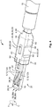
- Fig. 1 shows a perspective view of the cover assembly 1 according to one possible embodiment of the present disclosure, the cover assembly 1 comprising a protective cover 4 shown in a transparent depiction.
- the cover assembly 1 further comprises a first wire 6a of a shielded electric cable 10, a second wire 6b of the same shielded electric cable 10, a first contact element 12a of a connector 2, a second contact element 12b of the same connector 2, and a contact carrier 16.
- the protective cover 4 is a substantially cuboid part made of an insulation material with a relative permittivity higher than air. More particularly, the protective cover 4 may be an overmolded part 18, as shown in the embodiments of Figs. 1 to 4 .
- the contact carrier 16 is also a substantially cuboid part made of an insulation material with a relative permittivity higher than air.
- the contact carrier 16 comprises a contact section 20 with a traverse cross-sectional area smaller than the protective cover 4 and a bulged section 22 with a traverse cross-sectional area equal to the protective cover 4.
- the contact carrier 16 may further comprise a step-like transition between the contact section 20 and the bulged section 22.
- the first wire 6a and the second wire 6b extend parallel to each other through the shielded electrical cable 10.
- the first wire 6a and the second wire 6b each comprise a terminal portion 24 protruding out of the shielded electrical cable 10 and extending into the protective cover 4 in a transmission direction T.
- the first contact element 12a and the second contact element 12b extend parallel to each other through the contact carrier 16 and into the protective cover 4 in opposite direction of the transmission direction T.
- the first contact element 12a and the second contact element 12b may each be an electrically conductive spring beam 26, which flatly extends along the transmission direction T.
- the spring beams 26 may be positioned spaced apart from each other.
- Each of the spring beams 26 may comprise a contact portion 28 on one end, a bonding portion 30 on the opposite end and a retention portion 32 in between the contact portion 28 and the bonding portion 30.
- the contact portion 28 may have a curved tip 34.
- the curved tip 34 may be a pin-like, arc-shaped part formed integrally by the material of the corresponding spring beam 26.
- the bonding portion 30 may comprise a bonding tab 36 protruding opposite to the transmission direction T as a continuation of the spring beam 26.
- the bonding tab 36 may be a plate-shaped part formed integrally by the material of the corresponding spring beam 26 and fixedly embedded within the protective cover 4.
- the retention portion 32 may be a straight segment of the corresponding spring beam 26 fixedly retained by the contact carrier 16.
- a first signal path 38a is jointly formed by the first wire 6a and the first contact element 12a
- a second signal path 38b is jointly formed by the second wire 6b and the second contact element 12b. More particularly, at a first bond location 42a, the terminal portion 24 of the first wire 6a is overlappingly bonded to the bonding tab 36 of the first contact element 12a, while at a second bond location 42b, the terminal portion 24 of the second wire 6b, is overlappingly bonded to the bonding tab 36 of the second contact element 12b.
- the first bond location 42a and the second bond location 42b each possess a traverse cross-sectional area perpendicular to the transmission direction T, which is larger than the traverse cross-sectional area of the first wire 6a, the second wire 6b, the first contact element 12a or the second contact element 12b, respectively. Therefore, the first bond location 42a and the second bond location 42b each affect the impedance of the first signal path 38a and the second signal path 38b. In addition, the first bond location 42a and the second bond location 42b are both aligned and located within the protective cover 4.
- the insulation material of the protective cover 4 which surrounds the first signal path 38a and the second signal path 38b, also affects the impedance of the first signal path 38a and the second signal path 38b.
- at least one impedance control structure 46 may be implemented on the protective cover 4.
- the at least one impedance control structure 46 may be at least one recess 44 locally formed on the outer surface 40 of the protective cover 4 in an area, where the first signal path 38a and the second signal path 38b are surrounded by the insulation material of the protective cover 4, while the first signal path 38a and the second signal path 38b exhibit an increased cross-section.
- the at least one recess 44 may result in air-filled space in said area.
- the at least one recess 44 may be e.g. a substantially cuboid, cylindrical, conic, semi-spherical, trapezoidal or stadium-shaped cut-out in the insulation material of the protective cover4.
- the cut-out may at least partly extend towards the first signal path 38a and/or the second signal path 38b.
- the cut-out may extend into another direction, preferably the transmission direction T, at least along the entire length of the first bond location 42a and/or the second bond location 42b.
- the protective cover 4 may comprise a lead-through hole 48 as an impedance control structure 46, which extends as a substantially stadium-shaped cavity 50 through the insulation material of the protective cover 4. More particularly, the lead-through hole 48 may extend in a direction perpendicular to the transmission direction T, connecting a top surface 54 of the protective cover 4 with a bottom surface 56 of the protective cover 4. Moreover, the lead-through hole 48 may extend between the first bond location 42a and the second bond location 42b, forming an air-filled gap 58 there in between.
- the lead-through hole 48 may alternatively extend as a substantially cuboid cavity 52 through the insulation material of the protective cover 4.
- the lead-through hole 48 may also extend in a direction perpendicular to the transmission direction T connecting a top surface 54 of the protective cover 4 with a bottom surface 56 of the protective cover 4.
- the lead-through hole 48 may extend between the first bond location 42a and the second bond location 42b, forming an air-filled gap 58 thereinbetween.
- the protective cover 4 may comprise a pair of lateral recesses 60 as an impedance control structure 46, which may be implemented as an addition or alternative to the lead-through hole 48.
- the pair of lateral recesses 60 may extend symmetrically on two opposite side surfaces 62 of the protective cover 4, preferably two side surfaces 62, which span perpendicularly between the top surface 54 and the bottom surface 56.
- each of the pair of lateral recesses 60 may extend in the transmission direction T at least along the entire length of the first bond location 42a and the second bond location 42b. Further, in a direction parallel to the lead-through hole 48, the pair of lateral recesses 60 may extend along the entire length of the lead-through hole 48.
- each of the pair of lateral recesses 60 may be a trapezoidal cut-out 64 in the insulation material of the protective cover 4, extending perpendicularly to the transmission direction T and parallel to the lead-through hole 48.
- the cut-outs 64 may preferably extend along the entire height of the respective side surfaces 62, the height being the dimension in a direction perpendicular to the transmission direction T and parallel to the lead-through hole 48. Due to the trapezoidal shape of the cut-outs 64, each of the pair of lateral recesses 60 may have two chamfered edges 66 aligned along the transmission direction T.
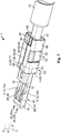
- Figs. 5 and 6 show an alternative embodiment of the protective cover 4, comprising two pieces 68 that are connected to each other to form the protective cover 4.
- the protective cover 4 may be formed jointly by a pair of pre-fabricated cover halves 70 engaging in a form-fit.
- the cover halves 70 are identical to each other, due to a hermaphrodite design, and comprise a latching mechanism 72, in that two latching cams 74 and two latching grooves 76 are arranged on each of the cover halves 70.
- the latching cams 74 project away from the respective cover halves 70 in a direction perpendicular to the transmission direction T and are each configured to engage in a latched connection with one of the two latching grooves on the respective other cover half 70.
- each latching groove has a shape complementary to the shape of the respective latching cam 74.
- the pair of cover halves 70 may comprise an impedance control structure 46 in that a high permittivity insulation material is used to form at least a part of each cover half 70.
- a high permittivity insulation material is used to form at least a part of each cover half 70.
- an insulation material with incorporated ceramic powder may be used as a high permittivity insulation material.
- Each of the pair of cover halves 70 may further comprise an inner wall 78, at least partly spacing apart the first signal path 38a from the second signal path 38b.
- the inner wall 78 may also be formed in the overmolded part 18, as can be seen in Figs. 1 to 4 .
- Fig. 7 shows another possible embodiment of an impedance control structure 46, in that the pair of pre-fabricated cover halves 70 is surrounded by two capacitive elements 80. More particularly, the two capacitive elements 80 are two metal clips 82, each made from a bent sheet metal part 84. The metal clips each comprise a top plate 86, a middle plate 88, and a bottom plate 90 arranged in a U-shaped manner.
- top plate 86 and the bottom plate 90 abut against the pair of pre-fabricated cover halves 70 and are in direct contact therewith.
- the middle plate 88 may be split into at least two segments, which are embedded into corresponding holding grooves 92 on the side surfaces 62 of the pair of pre-fabricated cover halves 70.
- the capacitive elements 80 may be separate metal plates (not shown) positioned into holding grooves 92 on at least one outer surface of the protective cover 4, or glued thereto. Furthermore, the capacitive elements 80 may be woven metal parts (not shown) surrounding the pair of pre-fabricated cover halves 70.
- the contact carrier 16 and the protective cover 4 may be positioned adjacently to each other in the transmission direction T, and engage in a form-fit.
- the protective cover 4 may comprise two tabs 94 protruding away from the protective cover 4 towards the contact carrier 16.
- the contact carrier 16 may comprise two complementarily-shaped slots, each configured to receive one of the two tabs 94 of the protective cover 4.
- the allocation of the tabs 94 and slots 96 may also be inverted, in that the contact carrier 16 comprises the tabs 94, and the protective cover 4 comprises the slots 96.
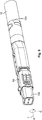
- Fig. 8 shows a sectional view of a connector 2 for high-frequency data transmission comprising the cover assembly 1 and a terminal shield 98, wherein the protective cover 4 and the contact carrier 16 of the cover assembly 1 are located within the terminal shield 98.
- the terminal shield 98 may comprise one insertion opening 100 for receiving a mating connector 102.
- the connector 2 may further be connected to a shielded electrical cable 10, preferably through a crimping connection.
- the terminal shield 98 may further comprise a crimping portion 104 on an end opposite to the insertion opening 100.
- the crimping portion 104 may be formed as an integral part of the terminal shield 98, and may extend coaxially with the shielded electrical cable 10.
- the crimping portion 104 may be wrapped around the shielded electrical cable in a circumferential direction C, as can be seen from Figs. 8 and 9 .
- Fig. 10 the result of providing a first contact element 12a in a 360° accessible orientation and providing a second contact element 12b in a 360° accessible orientation according to one embodiment of the method, disclosed in the present invention, is shown.
- the first contact element 12a and the second contact element 12b are provided in a 360° accessible orientation, in that the bonding tab 36 of the first contact element 12a and the bonding tab 36 of the second contact element 12b freely protrude away from the contact carrier 16.
- Fig. 11 the result of providing a first wire 6a in a 360° accessible orientation and providing a second wire 6b in a 360° accessible orientation, according to one embodiment of the method disclosed in the present invention, is shown.
- the first wire 6a and the second wire 6b are provided in a 360° accessible orientation, in that the terminal portion 24 of the first wire 6a and the terminal portion 24 of the second wire 6b freely protrude away from the shielded electrical cable 10.
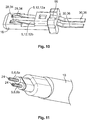
- Fig. 12 the preparations for the step of surrounding the first signal path 38a and the second signal path 38b with a cast 106, according to one embodiment of the method disclosed in the present invention, are shown.
- the terminal portion 24 of the first wire 6a is overlappingly bonded to the bonding tab 36 of the first contact element 12a at the first bond location 42a.
- the terminal portion 24 of the second wire 6b is overlappingly bonded to the bonding tab 36 of the second contact element 12b at the second bond location 42b.
- the cast 106 comprising two mold halves 108a, 108b, two cores 110, and a blade 112 is shown ready to surround the first bond location 42a and the second bond location 42b.
- the blade 112 may be inserted between the first bond location 42a and the second bond location 42b.
- the blade 112 may be positioned on one of the two cores 110, which fixate the first bond location 42a and the second bond location 42b from two opposite directions, perpendicular to the transmission direction T.
- the two cores 110 and the blade 112 preferably may possess a combined shape, which corresponds to the negative shape of the lead-through hole 48.
- the two cores 110 and the blade 112 may jointly form the lead-through opening 48 in the insulation material of the protective cover 4.
- Fig. 1 shows the result of removing the cast 106 after the hardening of the injected insulation material. More particularly, insulation material is injected into the cast 106, surrounding the first bond location 42a and second bond location 42b. After the hardening of the injected insulation material, the cast 106 is removed, resulting in the protective cover 4 being formed as an overmolded part 18 with at least one impedance control structure 46, namely the lead-through hole 48.
Landscapes
- Engineering & Computer Science (AREA)
- Manufacturing & Machinery (AREA)
- Details Of Connecting Devices For Male And Female Coupling (AREA)
- Coupling Device And Connection With Printed Circuit (AREA)
- Connector Housings Or Holding Contact Members (AREA)
Abstract
Description
- The present invention relates to a cover assembly and, more particularly, to a cover assembly for the protection of a bond between electrical conductors of a high-frequency data transmission line, in particular with operation frequencies in the gigahertz range.
- In the field of data transmission, transmission lines usually consist of multiple components such as connectors, cables, wires, receptacles, and the like. These transmission line components are interconnected in order to establish the necessary signal channel. Said interconnections can be realized through a connection means, e.g. a plug and socket mechanism, or a permanent bond. The connection means need to provide for a reliable electrical contact between the transmission line components. In case of permanent bonds, a reinforcement means is further provided, surrounding the permanent bond to increase the mechanical stability of the permanent bond.
- In applications where high-frequency data transmission is required, the connection means and the reinforcement means themselves may have a negative influence on the properties of the signal channel, which deteriorates the signal quality and transmission performance, respectively.
- The object of the present invention is to provide a means for reliably transmitting high-frequency signals in particular in the gigahertz range.
- The problem is solved by providing at least one impedance control structure in a cover assembly, comprising a protective cover and at least two electrical conductors for conducting electrical signals of a high-frequency data transmission, wherein the at least two electrical conductors extend through the protective cover in a transmission direction and are overlappingly bonded to each other at at least one bond location, which is located within the protective cover. The at least one bond location and the protective cover affect the impedance of the at least two electrical conductors. Therefore, the problem is solved particularly by providing at least one impedance control structure on the protective cover in order to adjust the impedance of the at least two electrical conductors to a predefined value according to the frequency of the data transmission.
- Thus, the effects of the at least one bond location and of the protective cover are compensated for.
- In general, impedance is the property of electrical conductors measuring their resistance against the flow of an alternating current. Impedance is influenced by several factors, such as the material and dimensions of the electrical conductor itself, by the mean relative permittivity of the medium surrounding the conductor (dielectric material), and by other electrically conductive or capacitive components in proximity of the electrical conductor, especially the relative distance between the respective surfaces.
- If during the transmission of an electrical signal from a signal source to a signal receiver (load) via a transmission line, the impedance of the load and the impedance of the transmission line is not matched (impedance mismatch), signal reflection may occur. Signal reflection impairs signal integrity and is therefore an unwanted phenomenon. The cause of such an impedance mismatch and subsequent signal reflection may be a non-linear change in the cross-section of an electrical conductor of the transmission line or a discontinuity in the material surrounding the electrical conductor as well as a sharp bend in the course of the transmission line.
- It is therefore preferable to match the impedance of the transmission line to the impedance of the load and to eliminate causes of impedance mismatch. In other words, it is preferable to adjust the impedance of the transmission line to a predefined value. Such a predefined value may be the impedance of the load.
- The above-mentioned solution is favorable, since it compensates for at least one cause of impedance mismatch and thus reduces signal reflection. Therefore, the signal integrity of the transmitted signal is substantially improved and the reliability of the signal transmission increased.
- The above solution may be further improved by adding one or more of the following optional features. Hereby, each of the following optional features is advantageous on its own, and may be combined independently with any other optional feature.
- According to a first embodiment, one of the at least two electrical conductors may be a wire of an electric cable, preferably a wire of a shielded electric cable comprising at least one stripped end. The respective other one of the at least two electrical conductors may be a contact element of a connector, preferably a pin-like contact element of a shielded connector. In this embodiment, the wire and the contact element may jointly form a signal path for the high-frequency data transmission.
- As will be described in detail further below, the signal path possesses an impedance amounting to a predefined value, due to the at least one impedance control structure. Thus, the cover assembly may serve as a protection for a bond between a shielded electric cable and a shielded connector.
- More particularly, the wire may comprise at least one terminal portion, wherein the at least one terminal portion may project away from the at least one stripped end of the shielded electrical cable into the protective cover. The contact element may comprise at least one bonding portion with at least one bonding tab, wherein the at least one bonding tab may project away from the at least one bonding portion into the protective cover. The at least one terminal portion may further at least partly overlap with the at least one bonding tab at the at least one bonding location within the protective cover. Furthermore, the at least one terminal portion may at least partly be bonded to the at least one bonding tab at the at least one bonding location within the protective cover.
- This embodiment enables the cover assembly to be used in combination with an electric cable, which allows the data transmission to take place over a longer distance, and thus increases the functionality of the present invention. Furthermore, this embodiment enables the cover assembly to be used in combination with a connector, thus further broadening the applicability of the present invention.
- Optionally, the cover assembly may comprise a first wire of an electric cable, a second wire of the same electric cable, a first contact element of a connector and a second contact element of the same connector, wherein the first wire and the first contact element jointly form a first signal path, while the second wire and the second contact element jointly form a second signal path, and the first signal path and the second signal path form a pair of signal paths. Preferably, the pair of signal paths may be positioned spaced apart and electrically isolated from each other. Furthermore, each of the pair of signal paths may be configured to transmit one signal of a differential pair of signals for high-frequency data transmission.
- As will be described in detail further below, the pair of signal paths possess an impedance amounting to a predefined value, due to the at least one impedance control structure. Thus, the cover assembly may serve as a protection for a bond between a shielded Twinax cable and a shielded Twinax connector.
- More particularly, the first and second wire each may comprise at least one terminal portion, wherein the terminal portions may project away from the electric cable into the protective cover in a spaced-apart arrangement. The first and second contact element each may comprise at least one bonding portion. Each bonding portion may comprise at least one bonding tab, which may project away from the respective bonding portion into the protective cover. The at least one terminal portion of the first wire may at least partly overlap with the at least one bonding tab of the first contact element at a first bonding location within the protective cover, while the at least one terminal portion of the second wire may at least partly overlap with the at least one bonding tab of the second contact element at a second bonding location within the protective cover. Furthermore, the at least one terminal portion of the first wire may at least partly be bonded to the at least one bonding tab of the first contact element at the first bonding location within the protective cover, while the at least one terminal portion of the second wire may at least partly be bonded to the at least one bonding tab of the second contact element at the second bonding location within the protective cover.
- This embodiment allows for data transmission that is less prone to electromagnetic noise, due to the transmission of a differential pair of signals.
- Additionally, the centerlines of the pair of signal paths may be parallel to each other along the entire length of the cover assembly. More particularly, the wire pitch of the first and second wire may be equal to the contact pitch of the first and second contact element. This embodiment especially prevents a spreading of the wires, which would lead to a sharp bend. Thus, at least one possible cause of signal reflection is eliminated in order to further improve signal integrity.
- According to another embodiment, the protective cover may be overmolded over the at least one bond location and made from insulation material, preferably an insulation material with a relative permittivity higher than air. Additionally, the overmold may exceed over a part of each of the at least two electrical conductors. More particularly, the at least two electrical conductors may be at least partly embedded within the overmold.
- This embodiment allows the protective cover to be manufactured through an automated low-pressure overmolding process. Thus, this embodiment contributes to the facilitation of the manufacturing process.
- According to an alternative embodiment, the protective cover may comprise at least two pieces that are connected to each other to form the protective cover. More particularly, the protective cover may be formed jointly by a pair of pre-fabricated cover halves engaging in a form-fit. Preferably, the pair of pre-fabricated cover halves may comprise a latching mechanism, in that at least one latching cam and at least one latching groove is arranged on each of the cover halves, and the at least one latching cam on each of the cover halves is configured to engage into a latched connection with the at least one latching groove on the respective other cover half.
- This embodiment allows the protective cover to be assembled through an automated pick and place assembly process. Thus, this embodiment provides an alternative, which also contributes to the facilitation of the manufacturing process.
- Optionally, the cover halves may be identical to each other. Preferably, the cover halves possess a hermaphrodite design, which further facilitates the manufacturing process, since a distinction between different types of cover halves is not necessary.
- Additionally or alternatively, the protective cover may comprise an inner wall at least partly spacing apart one of the pair of signal paths from the other of the pair of signal paths. This embodiment prevents direct contact between the pair of signal paths, lowering the risk for an electrical short.
- In yet another embodiment, the at least one impedance control structure may comprise or be at least one recess of an outer surface of the protective cover. The at least one recess is an impedance control structure that allows for an easy adjustment of at least one impedance-influencing factor, namely the mean relative permittivity of the dielectric material.
- More particularly, the recess may be locally formed on the outer surface of the protective cover in areas where the impedance of the at least two electrical conductors needs to be increased in order to arrive at the predefined value, and to compensate for the influence of the at least one bond location and of the protective cover. This could be the case, for example, in areas where the at least two electrical conductors are surrounded by an insulation material with a relative permittivity higher than air, while the at least two electrical conductors exhibit an increased cross-section, e.g. due to overlapping. In such an area, the recess will result in air-filled space. Since air has a lower relative permittivity than the insulation material, the resulting lower mean relative permittivity of the dielectric material (part air, part insulation material) will cause an increase of impedance of the at least two electrical conductors.
- Additionally or alternatively, the at least one impedance control structure may comprise or be at least one lead-through hole in the protective cover that connects at least two outer surfaces of the protective cover. Preferably, the at least one lead-through hole may extend as a cylindrical, cuboid, or stadium-shaped cavity through the insulation material in a direction perpendicular to the transmission direction.
- The at least one lead-through hole is also an impedance control structure that allows for an easy adjustment of at least one impedance-influencing factor, namely the mean relative permittivity of the dielectric material. In combination with the embodiment comprising a pair of signal paths, the at least one lead-through hole may preferably extend between the pair of signal paths. This way, an air-filled space may be created between the pair of signal paths, which results in a lower mean relative permittivity of the dielectric material and in an increased impedance of the pair of signal paths, since air has a lower relative permittivity than the insulation material. Therefore, the at least one lead-through hole may be implemented in applications where the impedance of the pair of signal paths needs to be increased in order to arrive at the predefined value and to compensate for the influence of the at least one bond location and of the protective cover.
- Optionally, the at least one impedance control structure may comprise or be at least one lateral recess of a side surface of the protective cover. Preferably, at least one pair of lateral recesses may extend symmetrically on two opposite side surfaces of the protective cover. Furthermore, each of the pair of lateral recesses may extend in the transmission direction at least along the entire length of the bond location. Further, in a direction parallel to the lead-through hole the at least one pair of lateral recesses may extend along the entire length of the lead-through hole.
- More particularly, each of the pair of lateral recesses may be a trapezoidal, cuboid or round cut-out in the insulation material of the protective cover extending perpendicularly to the transmission direction and parallel to the lead-through hole. The cut-outs may preferably extend along the entire height of the respective side surfaces, the height being the dimension in a direction perpendicular to the transmission direction and parallel to the lead-through hole.
- Optionally, each of the pair of lateral recesses may have at least one chamfered edge at its end in the transmission direction. The at least one chamfered edge improves the manufacturability of the lateral recesses during a casting process, since it functions as a draft, facilitating the demolding step.
- In yet another embodiment, the at least one impedance control structure may comprise or be at least one capacitive element, preferably an electrically conductive capacitive element positioned on at least one outer surface of the protective cover. More particularly, the at least one capacitive element may be a metal plate positioned in a holding groove on at least one outer surface of the protective cover, or glued thereto.
- In the embodiment comprising the pair of pre-fabricated cover halves, the at least one capacitive element may alternatively be at least one metal clip, bent sheet metal part or woven metal part holding together the pair of pre-fabricated cover halves. More particularly, the pair of pre-fabricated cover halves may at least partly be surrounded by and in direct contact with the metal clip, the bent sheet metal part or the woven metal part.
- The at least one capacitive element is an impedance control structure that allows for an adjustment of at least one impedance-influencing factor, namely the relative distance between the surfaces of the at least two electrical conductors and the surface of the at least one capacitive element. In particular, said relative distance is shortened by positioning the at least one capacitive element on the surface of the protective cover and thus in proximity of the at least two electrical conductors. As a result, the impedance of the at least two electrical conductors is lowered. Subsequently, the at least one capacitive element may be utilized in applications where the impedance of the at least two electrical conductors needs to be reduced in order to arrive at the predefined value, and to compensate for the influence of the at least one bond location and of the protective cover. This could be the case, for example, in areas where the at least two electrical conductors are surrounded by air, e.g. due to air-filled gaps in the protective cover caused be manufacturing inaccuracies.
- As an addition or alternative for the same case, the at least one impedance control structure may comprise a usage of a high permittivity insulation material for the protective cover, preferably a material with a relative permittivity in a range between 9 and 10. More particularly, an insulation material with incorporated ceramic powder may be used as the high permittivity insulation material for the protective cover. The usage of a high permittivity insulation material may result in a higher mean relative permittivity of the dielectric material (part air, part high permittivity insulation material), which will cause a decrease of impedance of the at least two electrical conductors.
- Optionally, any of the above-mentioned embodiments of the at least one impedance control structure may be aligned with the at least one bond location. More particularly, the at least one impedance control structure may be in the vicinity of and/or locally limited to the area of influence of the at least one bond location, thus concentrating and maximizing the effect of the at least one impedance control structure.
- According to yet another embodiment of the present invention, the cover assembly may further comprise a contact carrier for supporting at least one of the at least two electrical conductors, wherein one end of the corresponding electrical conductor protrudes from the contact carrier freely into the material of the protective cover. More particularly, said end comprises a straight tab, which is fixedly embedded in the protective cover.
- The contact carrier may be at least one separate component engaging in a form-fit with the protective cover. For this, the contact carrier may comprise a socket or slot for receiving a tab or knob positioned on the protective cover. Alternatively, the contact carrier may be formed as an integral part of the protective cover.
- This embodiment is advantageous in that it provides additional structural support to at least one of the at least two electrical conductors through the contact carrier.
- According to another embodiment, the cover assembly may be part of a connector for high-frequency data transmission further comprising a terminal shield, wherein the protective cover and the contact carrier of the cover assembly are located within the terminal shield. The terminal shield may comprise at least one insertion opening for receiving a mating connector, wherein the mating connector is preferably configured to be brought into electrical contact with at least one of the at least two electrical conductors upon insertion into the opening of the terminal shield.
- This embodiment enables the cover assembly to be used in combination with a mating connector, thus further broadening the applicability of the present invention.
- The technical problem is also solved by providing a method for overmolding a bond between at least one wire of a cable and at least one contact element with a protective cover made of insulation material, preferably polyamide. The method comprises steps of providing the at least one contact element; providing the at least one wire; positioning the at least one contact element and the at least one wire in a partially overlapping position; bonding the at least one contact element and the at least one wire e.g. by welding, preferably by compaction welding and/or resistive welding or alternatively by similar appropriate methods such as soldering, brazing, etc.; surrounding the bonds with a cast, the cast comprising at least one core, which forms the at least one impedance control structure in the insulation material; injecting the insulation material into the cast; and removing the cast and the at least two cores after the hardening of the injected insulation material.
- This method allows the manufacturing of the protective cover as the overmolded part, thus proving a means for reliably transmitting high-frequency signals, in particular in the gigahertz range. Simultaneously, this method allows forming the at least one impedance control structure in the insulation material of the protective cover. It therefore shortens the time for manufacturing of the overmolded protective cover.
- The above described method may be further improved by adding one or more of the following optional steps. Hereby, each of the following optional steps is advantageous on its own, and may be combined independently with any other optional step.
- In a first embodiment, the method may comprise the steps of providing the at least one contact element, preferably in a 360° accessible orientation; and providing the at least one wire, preferably in a 360° accessible orientation.
- By providing the at least one contact element and the at least one wire in a 360° accessible orientation, it is possible to implement a resistive welding process, wherein the at least one contact element and the at least one wire may be overlappingly placed between two ceramic spacers and pinched between two electrodes, which establish an electrical current in and a mechanical force on the overlapping at least one contact element and at least one wire. Such a resistive welding process exhibits short cool-down periods and thus increases productivity. It also may be realized in small scale applications, thus enabling miniaturized design.
- In another embodiment, the method may comprise the steps of providing a first contact element; providing a second contact element; providing a first wire; providing a second wire; positioning the first contact element and the first wire in a partially overlapping position, to form a first signal path; and positioning the second contact element and the second wire in a partially overlapping position, to form a second signal path.
- This embodiments allows the production of a pair of signal paths, which may be configured each to transmit one signal of a differential pair of signals for high-frequency data transmission. Thus a data transmission that is less prone to electromagnetic noise, due to the transmission of a differential pair of signals, may be realized.
- In yet another embodiment the method may comprise the steps of fixating the first and second signal path with at least two cores from at least two opposite directions, preferably two opposite directions perpendicular to the transmission direction.
- Securing the first and second signal path with the at least two cores from at least two opposite directions prevents an unwanted movement of the first and second signal path during the injection of the insulation material, thus increasing the reliability of the overmolding process.
- According to another embodiment, the method may comprise the steps of inserting a blade between the first and second signal path, the blade preferably being an integral part of one of the at least two cores.
- The blade may function as an additional or alternative spacer between the first and second signal path, further preventing an unwanted movement of the first and second signal path during the injection of the insulation material. The blade thus may further increase the reliability of the overmolding process.
- Moreover, a combination of the at least two cores and the blade allows for the manufacturing of the overmolded protective cover itself, while simultaneously forming the at least one lead-through hole as an impedance control structure in the insulation material of the protective cover.
- In the following, exemplary embodiments of the invention are described with reference to the drawings. The shown and described embodiments serve explanatory purposes only. The combination of features shown in the embodiments may be changed according to the foregoing description. For example, a feature which is not shown in an embodiment but described above may be added, if the technical effect associated with this feature is beneficial for a particular application. Vice versa, a feature shown as part of an embodiment may be omitted as described above, if the technical effect associated with this feature is not needed in a particular application.
- In the drawings, elements that correspond to each other with respect to function and/or structure have been provided with the same reference numeral.
- In the drawings:
- Fig. 1
- shows a schematic rendition of a perspective, a partially transparent view of a cover assembly, and a shielded cable according to one possible embodiment of the present disclosure;
- Fig. 2
- shows a partially enlarged schematic view of
Fig. 1 ; - Fig. 3
- shows a schematic rendition of a perspective, a partially transparent view of a cover assembly, and a shielded cable according to another possible embodiment of the present disclosure;
- Fig. 4
- shows a schematic rendition of a perspective view of the cover assembly and the shielded cable according to the embodiment shown in
Fig. 3 ; - Fig. 5
- shows a schematic rendition of an exploded view of a cover assembly and a shielded cable according to another possible embodiment of the present disclosure;
- Fig. 6
- shows a schematic rendition of a perspective view of the cover assembly and the shielded cable according to the embodiment shown in
Fig. 5 ; - Fig. 7
- shows a schematic rendition of a perspective view of a cover assembly and a shielded cable according to another possible embodiment of the present disclosure;
- Fig. 8
- shows a schematic rendition of a sectional view of a connector according to one possible embodiment of the present disclosure;
- Fig. 9
- shows a schematic rendition of a perspective view of the connector according to the embodiment shown in
Fig. 8 and a mating connector; - Fig. 10
- shows a schematic rendition of a perspective view of a contact carrier according to one possible embodiment of the present disclosure;
- Fig. 11
- shows a schematic rendition of a perspective view of a shielded electrical cable according to one possible embodiment of the present disclosure; and
- Fig. 12
- shows a schematic rendition of a perspective view of a contact carrier, a shielded electrical cable and a cast according to one possible embodiment of the present disclosure.
- First, the structure of a
cover assembly 1 according to the present invention is explained with reference to the exemplary embodiments shown inFigs. 1 to 7 .Figs. 8 and9 are used for explaining the structure of aconnector 2 according to the present invention.Figs. 10 to 12 are used for explaining the method according to the present invention. -
Fig. 1 shows a perspective view of thecover assembly 1 according to one possible embodiment of the present disclosure, thecover assembly 1 comprising a protective cover 4 shown in a transparent depiction. Thecover assembly 1 further comprises a first wire 6a of a shieldedelectric cable 10, a second wire 6b of the same shieldedelectric cable 10, a first contact element 12a of aconnector 2, a second contact element 12b of thesame connector 2, and acontact carrier 16. - The protective cover 4 is a substantially cuboid part made of an insulation material with a relative permittivity higher than air. More particularly, the protective cover 4 may be an overmolded part 18, as shown in the embodiments of
Figs. 1 to 4 . - The
contact carrier 16 is also a substantially cuboid part made of an insulation material with a relative permittivity higher than air. Thecontact carrier 16 comprises acontact section 20 with a traverse cross-sectional area smaller than the protective cover 4 and a bulgedsection 22 with a traverse cross-sectional area equal to the protective cover 4. Thecontact carrier 16 may further comprise a step-like transition between thecontact section 20 and the bulgedsection 22. - The first wire 6a and the second wire 6b extend parallel to each other through the shielded
electrical cable 10. On one end, the first wire 6a and the second wire 6b each comprise aterminal portion 24 protruding out of the shieldedelectrical cable 10 and extending into the protective cover 4 in a transmission direction T. - The first contact element 12a and the second contact element 12b extend parallel to each other through the
contact carrier 16 and into the protective cover 4 in opposite direction of the transmission direction T. - As shown in
Figs. 1 and3 , the first contact element 12a and the second contact element 12b may each be an electrically conductive spring beam 26, which flatly extends along the transmission direction T. The spring beams 26 may be positioned spaced apart from each other. Each of the spring beams 26 may comprise a contact portion 28 on one end, a bonding portion 30 on the opposite end and aretention portion 32 in between the contact portion 28 and the bonding portion 30. - The contact portion 28 may have a curved tip 34. The curved tip 34 may be a pin-like, arc-shaped part formed integrally by the material of the corresponding spring beam 26.
- The bonding portion 30 may comprise a bonding tab 36 protruding opposite to the transmission direction T as a continuation of the spring beam 26. The bonding tab 36 may be a plate-shaped part formed integrally by the material of the corresponding spring beam 26 and fixedly embedded within the protective cover 4.
- The
retention portion 32 may be a straight segment of the corresponding spring beam 26 fixedly retained by thecontact carrier 16. - As can be seen in
Figs. 1 and2 , a first signal path 38a is jointly formed by the first wire 6a and the first contact element 12a, while a second signal path 38b is jointly formed by the second wire 6b and the second contact element 12b. More particularly, at afirst bond location 42a, theterminal portion 24 of the first wire 6a is overlappingly bonded to the bonding tab 36 of the first contact element 12a, while at asecond bond location 42b, theterminal portion 24 of the second wire 6b, is overlappingly bonded to the bonding tab 36 of the second contact element 12b. - The
first bond location 42a and thesecond bond location 42b each possess a traverse cross-sectional area perpendicular to the transmission direction T, which is larger than the traverse cross-sectional area of the first wire 6a, the second wire 6b, the first contact element 12a or the second contact element 12b, respectively. Therefore, thefirst bond location 42a and thesecond bond location 42b each affect the impedance of the first signal path 38a and the second signal path 38b. In addition, thefirst bond location 42a and thesecond bond location 42b are both aligned and located within the protective cover 4. Due to its role as a dielectric material, the insulation material of the protective cover 4, which surrounds the first signal path 38a and the second signal path 38b, also affects the impedance of the first signal path 38a and the second signal path 38b. In order to compensate for said effects on thefirst bond location 42a, thesecond bond location 42b, and the protective cover 4, at least one impedance control structure 46 may be implemented on the protective cover 4. - For example, the at least one impedance control structure 46 may be at least one recess 44 locally formed on the
outer surface 40 of the protective cover 4 in an area, where the first signal path 38a and the second signal path 38b are surrounded by the insulation material of the protective cover 4, while the first signal path 38a and the second signal path 38b exhibit an increased cross-section. In particular, the at least one recess 44 may result in air-filled space in said area. For this, the at least one recess 44 may be e.g. a substantially cuboid, cylindrical, conic, semi-spherical, trapezoidal or stadium-shaped cut-out in the insulation material of the protective cover4. The cut-out may at least partly extend towards the first signal path 38a and/or the second signal path 38b. Furthermore, the cut-out may extend into another direction, preferably the transmission direction T, at least along the entire length of thefirst bond location 42a and/or thesecond bond location 42b. - Additionally or alternatively, the protective cover 4 may comprise a lead-through hole 48 as an impedance control structure 46, which extends as a substantially stadium-shaped cavity 50 through the insulation material of the protective cover 4. More particularly, the lead-through hole 48 may extend in a direction perpendicular to the transmission direction T, connecting a
top surface 54 of the protective cover 4 with abottom surface 56 of the protective cover 4. Moreover, the lead-through hole 48 may extend between thefirst bond location 42a and thesecond bond location 42b, forming an air-filledgap 58 there in between. - As shown in
Figs. 3 and4 , the lead-through hole 48 may alternatively extend as a substantially cuboid cavity 52 through the insulation material of the protective cover 4. In this embodiment, the lead-through hole 48 may also extend in a direction perpendicular to the transmission direction T connecting atop surface 54 of the protective cover 4 with abottom surface 56 of the protective cover 4. Moreover, the lead-through hole 48 may extend between thefirst bond location 42a and thesecond bond location 42b, forming an air-filledgap 58 thereinbetween. - As can further be seen from
Figs. 3 and4 , the protective cover 4 may comprise a pair of lateral recesses 60 as an impedance control structure 46, which may be implemented as an addition or alternative to the lead-through hole 48. In particular, the pair of lateral recesses 60 may extend symmetrically on two opposite side surfaces 62 of the protective cover 4, preferably twoside surfaces 62, which span perpendicularly between thetop surface 54 and thebottom surface 56. Furthermore, each of the pair of lateral recesses 60 may extend in the transmission direction T at least along the entire length of thefirst bond location 42a and thesecond bond location 42b. Further, in a direction parallel to the lead-through hole 48, the pair of lateral recesses 60 may extend along the entire length of the lead-through hole 48. - More particularly, each of the pair of lateral recesses 60 may be a trapezoidal cut-out 64 in the insulation material of the protective cover 4, extending perpendicularly to the transmission direction T and parallel to the lead-through hole 48. The cut-outs 64 may preferably extend along the entire height of the respective side surfaces 62, the height being the dimension in a direction perpendicular to the transmission direction T and parallel to the lead-through hole 48. Due to the trapezoidal shape of the cut-outs 64, each of the pair of lateral recesses 60 may have two chamfered
edges 66 aligned along the transmission direction T. -
Figs. 5 and6 show an alternative embodiment of the protective cover 4, comprising two pieces 68 that are connected to each other to form the protective cover 4. More particularly, the protective cover 4 may be formed jointly by a pair of pre-fabricated cover halves 70 engaging in a form-fit. Preferably, the cover halves 70 are identical to each other, due to a hermaphrodite design, and comprise a latching mechanism 72, in that two latchingcams 74 and two latching grooves 76 are arranged on each of the cover halves 70. The latchingcams 74 project away from the respective cover halves 70 in a direction perpendicular to the transmission direction T and are each configured to engage in a latched connection with one of the two latching grooves on the respective other cover half 70. For this, each latching groove has a shape complementary to the shape of therespective latching cam 74. - The pair of cover halves 70 may comprise an impedance control structure 46 in that a high permittivity insulation material is used to form at least a part of each cover half 70. Preferably, an insulation material with incorporated ceramic powder may be used as a high permittivity insulation material.
- Each of the pair of cover halves 70 may further comprise an
inner wall 78, at least partly spacing apart the first signal path 38a from the second signal path 38b. Theinner wall 78 may also be formed in the overmolded part 18, as can be seen inFigs. 1 to 4 . -
Fig. 7 shows another possible embodiment of an impedance control structure 46, in that the pair of pre-fabricated cover halves 70 is surrounded by two capacitive elements 80. More particularly, the two capacitive elements 80 are two metal clips 82, each made from a bent sheet metal part 84. The metal clips each comprise atop plate 86, amiddle plate 88, and abottom plate 90 arranged in a U-shaped manner. - More particularly, the
top plate 86 and thebottom plate 90 abut against the pair of pre-fabricated cover halves 70 and are in direct contact therewith. Themiddle plate 88 may be split into at least two segments, which are embedded into corresponding holdinggrooves 92 on the side surfaces 62 of the pair of pre-fabricated cover halves 70. - Alternatively, the capacitive elements 80 may be separate metal plates (not shown) positioned into holding
grooves 92 on at least one outer surface of the protective cover 4, or glued thereto. Furthermore, the capacitive elements 80 may be woven metal parts (not shown) surrounding the pair of pre-fabricated cover halves 70. - As can be seen from
Figs. 1 to 7 , thecontact carrier 16 and the protective cover 4 may be positioned adjacently to each other in the transmission direction T, and engage in a form-fit. For this, the protective cover 4 may comprise twotabs 94 protruding away from the protective cover 4 towards thecontact carrier 16. Thecontact carrier 16 may comprise two complementarily-shaped slots, each configured to receive one of the twotabs 94 of the protective cover 4. - The allocation of the
tabs 94 andslots 96 may also be inverted, in that thecontact carrier 16 comprises thetabs 94, and the protective cover 4 comprises theslots 96. -
Fig. 8 shows a sectional view of aconnector 2 for high-frequency data transmission comprising thecover assembly 1 and aterminal shield 98, wherein the protective cover 4 and thecontact carrier 16 of thecover assembly 1 are located within theterminal shield 98. Theterminal shield 98 may comprise oneinsertion opening 100 for receiving amating connector 102. - The
connector 2 may further be connected to a shieldedelectrical cable 10, preferably through a crimping connection. For this, theterminal shield 98 may further comprise a crimpingportion 104 on an end opposite to theinsertion opening 100. The crimpingportion 104 may be formed as an integral part of theterminal shield 98, and may extend coaxially with the shieldedelectrical cable 10. Furthermore, the crimpingportion 104 may be wrapped around the shielded electrical cable in a circumferential direction C, as can be seen fromFigs. 8 and9 . - In
Fig. 10 , the result of providing a first contact element 12a in a 360° accessible orientation and providing a second contact element 12b in a 360° accessible orientation according to one embodiment of the method, disclosed in the present invention, is shown. The first contact element 12a and the second contact element 12b are provided in a 360° accessible orientation, in that the bonding tab 36 of the first contact element 12a and the bonding tab 36 of the second contact element 12b freely protrude away from thecontact carrier 16. - In
Fig. 11 , the result of providing a first wire 6a in a 360° accessible orientation and providing a second wire 6b in a 360° accessible orientation, according to one embodiment of the method disclosed in the present invention, is shown. The first wire 6a and the second wire 6b are provided in a 360° accessible orientation, in that theterminal portion 24 of the first wire 6a and theterminal portion 24 of the second wire 6b freely protrude away from the shieldedelectrical cable 10. - In
Fig. 12 , the preparations for the step of surrounding the first signal path 38a and the second signal path 38b with a cast 106, according to one embodiment of the method disclosed in the present invention, are shown. In particular, theterminal portion 24 of the first wire 6a is overlappingly bonded to the bonding tab 36 of the first contact element 12a at thefirst bond location 42a. Theterminal portion 24 of the second wire 6b is overlappingly bonded to the bonding tab 36 of the second contact element 12b at thesecond bond location 42b. - Further, in
Fig. 12 , the cast 106 comprising two mold halves 108a, 108b, twocores 110, and ablade 112 is shown ready to surround thefirst bond location 42a and thesecond bond location 42b. In particular, theblade 112 may be inserted between thefirst bond location 42a and thesecond bond location 42b. Theblade 112 may be positioned on one of the twocores 110, which fixate thefirst bond location 42a and thesecond bond location 42b from two opposite directions, perpendicular to the transmission direction T. The twocores 110 and theblade 112 preferably may possess a combined shape, which corresponds to the negative shape of the lead-through hole 48. Thus, the twocores 110 and theblade 112 may jointly form the lead-through opening 48 in the insulation material of the protective cover 4. -
Fig. 1 shows the result of removing the cast 106 after the hardening of the injected insulation material. More particularly, insulation material is injected into the cast 106, surrounding thefirst bond location 42a andsecond bond location 42b. After the hardening of the injected insulation material, the cast 106 is removed, resulting in the protective cover 4 being formed as an overmolded part 18 with at least one impedance control structure 46, namely the lead-through hole 48. -
- 1
- cover assembly
- 2
- connector
- 4
- protective cover
- 5
- electrical conductor
- 6
- wire
- 6a
- first wire
- 6b
- second wire
- 10
- shielded electric cable
- 12
- contact element
- 12a
- first contact element
- 12b
- second contact element
- 16
- contact carrier
- 18
- overmolded part
- 20
- contact section
- 22
- bulged section
- 24
- terminal portion
- 26
- spring beam
- 28
- contact portion
- 30
- bonding portion
- 32
- retention portion
- 34
- curved tip
- 36
- bonding tab
- 38
- signal path
- 38a
- first signal path
- 38b
- second signal path
- 40
- outer surface
- 42
- bond location
- 42a
- first bond location
- 42b
- second bond location
- 44
- recess
- 46
- impedance control structure
- 48
- lead-through hole
- 50
- stadium-shaped cavity
- 52
- cuboid cavity
- 54
- top surface
- 56
- bottom surface
- 58
- air-filled gap
- 60
- lateral recess
- 62
- side surface
- 64
- cut-out
- 66
- chamfered edge
- 68
- piece
- 70
- pre-fabricated cover halves
- 72
- latching mechanism
- 74
- latching cam
- 76
- latching groove
- 78
- inner wall
- 80
- capacitive element
- 82
- metal clip
- 84
- bent sheet metal part
- 86
- top plate
- 88
- middle plate
- 90
- bottom plate
- 92
- holding grooves
- 94
- tab
- 96
- slot
- 98
- terminal shield
- 100
- insertion opening
- 102
- mating connector
- 104
- crimping portion
- 106
- cast
- 108
- mold halves (a, b)
- 110
- core
- 112
- Blade
- T
- transmission direction
- C
- circumferential direction
Claims (15)
- A cover assembly (1) comprising a protective cover (4) and at least two electrical conductors (5) for conducting electrical signals of a high-frequency data transmission, wherein
the at least two electrical conductors (5) extend through the protective cover (4) in a transmission direction (T) and are overlappingly bonded to each other at at least one bond location (42), which is located within the protective cover (4); and wherein
the protective cover (4) comprises at least one impedance control structure (46) that is configured to adjust the impedance of the at least one bond location (42) to a predefined value. - A cover assembly (1) according to claim 1, wherein
one of the at least two electrical conductors (5) is a wire (6) of a shielded electric cable (10); wherein
the other one of the at least two electrical conductors (5) is a pin-like contact element (12); and wherein
the wire (6) and the contact element (12) jointly form a signal path (38) for the transmission of data. - A cover assembly (1) according to claim 2, wherein
the cover assembly (1) comprises a first wire (6a), a second wire (6b), a first contact element (12a), and a second contact element (12b); wherein
the first wire (6a) and the first contact element (12a) jointly form a first signal path (38a); wherein
the second wire (6b) and the second contact element (12b) jointly form a second signal path (38b); and wherein
the first signal path (38a) and the second signal path (38b) form a pair of signal paths (38). - A cover assembly (1) according to claim 3, wherein
the centerlines of the pair of signal paths (38) run parallel to each other along the whole length of the cover assembly (1). - A cover assembly (1) according to any one of claims 1 to 4, wherein
the protective cover (4) is overmolded over the at least one bond location (42) and made from insulation material. - A cover assembly (1) according to any one of claims 1 to 4, wherein
the protective cover (4) comprises at least two pieces (68) that are connected to each other to form the protective cover (4). - A cover assembly (1) according to any one of claims 1 to 6, wherein
the at least one impedance control structure (46) comprises at least one recess (44) of an outer surface (40) of the protective cover (4). - A cover assembly (1) according to any one of claims 3 to 7, wherein
the at least one impedance control structure (46) comprises at least one lead-through hole (48) in the protective cover (4) that extends between the pair of signal paths (38). - A cover assembly (1) according to any one of claims 1 to 8, wherein
the at least one impedance control structure (46) comprises at least one lateral recess (60) of a side surface (62) of the protective cover (4). - A cover assembly (1) according to any one of claims 1 to 9, wherein
the at least one impedance control structure (46) comprises at least one capacitive element (80) positioned on at least one outer surface (40) of the protective cover (4). - A cover assembly (1) according to any one of claims 1 to 10, wherein
the at least one impedance control structure (46) comprises a usage of a high permittivity insulation material for the protective cover (4). - A cover assembly (1) according to any one of claims 1 to 11, wherein
the at least one impedance control structure (46) is aligned with the at least one bond location (42). - A cover assembly (1) according to any one of claims 1 to 12, wherein
the cover assembly (1) comprises a contact carrier (16) for supporting at least one of the at least two electrical conductors (5), wherein one end of the electrical conductor (5) protrudes from the contact carrier (16) into the protective cover (4). - A connector (2) comprising a cover assembly (1) according to any one of claims 1 to 13, a terminal shield (98) and a contact carrier (16), wherein
the protective cover (4) of the cover assembly (1) and the contact carrier (16) are located within the terminal shield (98); and wherein
the terminal shield (98) comprises at least one insertion opening (100) for receiving a mating connector (102). - A method for overmolding with insulation material a bond (42) between at least one contact element (12) and at least one wire (6) of a cable (10), comprising steps of providing the at least one contact element (12);
providing the at least one wire (6);
positioning the at least one contact element (12) and the at least one wire (6) in a partially overlapping position;
bonding the at least one contact element (12) and the at least one wire (6);
surrounding the bond (42) with a cast (106); the cast (106) comprising at least one core (110), which forms at least one impedance control structure (46) in the insulation material;
injecting the insulation material into the cast (106); and
removing the cast (106) and the at least two cores (110) after the hardening of the injected insulation material.
Priority Applications (6)
| Application Number | Priority Date | Filing Date | Title |
|---|---|---|---|
| EP19193937.0A EP3787117A1 (en) | 2019-08-27 | 2019-08-27 | Cover assembly with at least one impedance control structure |
| JP2020139028A JP2021034377A (en) | 2019-08-27 | 2020-08-20 | Cover assembly with at least one impedance control structure |
| KR1020200106966A KR102798611B1 (en) | 2019-08-27 | 2020-08-25 | Cover assembly with at least one impedance control structure |
| CN202010861780.4A CN112448237A (en) | 2019-08-27 | 2020-08-25 | Cap assembly having at least one impedance control structure |
| US17/004,539 US11355889B2 (en) | 2019-08-27 | 2020-08-27 | Cover assembly with at least one impedance control structure |
| JP2025034269A JP2025081755A (en) | 2019-08-27 | 2025-03-05 | Cover assembly having at least one impedance control structure |
Applications Claiming Priority (1)
| Application Number | Priority Date | Filing Date | Title |
|---|---|---|---|
| EP19193937.0A EP3787117A1 (en) | 2019-08-27 | 2019-08-27 | Cover assembly with at least one impedance control structure |
Publications (1)
| Publication Number | Publication Date |
|---|---|
| EP3787117A1 true EP3787117A1 (en) | 2021-03-03 |
Family
ID=67777108
Family Applications (1)
| Application Number | Title | Priority Date | Filing Date |
|---|---|---|---|
| EP19193937.0A Pending EP3787117A1 (en) | 2019-08-27 | 2019-08-27 | Cover assembly with at least one impedance control structure |
Country Status (5)
| Country | Link |
|---|---|
| US (1) | US11355889B2 (en) |
| EP (1) | EP3787117A1 (en) |
| JP (2) | JP2021034377A (en) |
| KR (1) | KR102798611B1 (en) |
| CN (1) | CN112448237A (en) |
Families Citing this family (4)
| Publication number | Priority date | Publication date | Assignee | Title |
|---|---|---|---|---|
| DE102020124893A1 (en) * | 2020-09-24 | 2022-03-24 | Md Elektronik Gmbh | CONNECTORS AND PROCESSES |
| JP7563322B2 (en) * | 2021-07-27 | 2024-10-08 | 株式会社オートネットワーク技術研究所 | connector |
| JP2023076964A (en) * | 2021-11-24 | 2023-06-05 | 株式会社オートネットワーク技術研究所 | connector |
| EP4432480A1 (en) * | 2023-03-14 | 2024-09-18 | TE Connectivity Solutions GmbH | Contact carrier, method of producing a contact carrier and apparatus for producing a contact carrier |
Citations (6)
| Publication number | Priority date | Publication date | Assignee | Title |
|---|---|---|---|---|
| US6203369B1 (en) * | 1999-10-25 | 2001-03-20 | 3M Innovative Properties Company | High frequency cable connector having low self-inductance ground return paths |
| EP2169770A2 (en) * | 2008-09-29 | 2010-03-31 | Amphenol Corporation | Ground sleeve having improved impedance control and high frequency performance |
| EP2884592A1 (en) * | 2013-12-10 | 2015-06-17 | Delphi Technologies, Inc. | Electrical connection system |
| US10283891B2 (en) * | 2017-03-08 | 2019-05-07 | Autonetworks Technologies, Ltd. | Shield terminal |
| US10305202B2 (en) * | 2017-03-08 | 2019-05-28 | Autonetworks Technologies, Ltd. | Shield terminal |
| US20190252806A1 (en) * | 2016-10-12 | 2019-08-15 | Autonetworks Technologies, Ltd. | Connector structure |
Family Cites Families (19)
| Publication number | Priority date | Publication date | Assignee | Title |
|---|---|---|---|---|
| US7004793B2 (en) * | 2004-04-28 | 2006-02-28 | 3M Innovative Properties Company | Low inductance shielded connector |
| US7731528B2 (en) * | 2006-01-31 | 2010-06-08 | 3M Innovative Properties Company | Electrical termination device |
| US7744403B2 (en) * | 2006-11-29 | 2010-06-29 | 3M Innovative Properties Company | Connector for electrical cables |
| JP4889569B2 (en) * | 2007-05-30 | 2012-03-07 | タイコエレクトロニクスジャパン合同会社 | Floating connector |
| US7722394B2 (en) * | 2008-02-21 | 2010-05-25 | 3M Innovative Properties Company | Electrical termination device |
| JP2010212017A (en) * | 2009-03-09 | 2010-09-24 | Japan Aviation Electronics Industry Ltd | Electric connector |
| US8192232B2 (en) * | 2009-09-15 | 2012-06-05 | Tyco Electronics Corporation | Connector assembly having an electrical compensation component |
| CN102916286B (en) * | 2011-08-02 | 2015-05-27 | 富士康(昆山)电脑接插件有限公司 | Electrical connector |
| JP5830394B2 (en) * | 2012-01-26 | 2015-12-09 | ホシデン株式会社 | Contact impedance adjustment method, contact and connector equipped with the same |
| DE102012005812A1 (en) * | 2012-03-22 | 2013-09-26 | Tyco Electronics Amp Gmbh | Electrical connector with integrated impedance matching element |
| US9608590B2 (en) * | 2014-11-18 | 2017-03-28 | Te Connectivity Corporation | Cable assembly having a signal-control component |
| JP6429078B2 (en) * | 2015-01-29 | 2018-11-28 | 株式会社オートネットワーク技術研究所 | Shield connector |
| US10511116B2 (en) * | 2016-01-13 | 2019-12-17 | Autonetworks Technologies, Ltd. | Connector |
| WO2017201170A1 (en) * | 2016-05-18 | 2017-11-23 | Amphenol Corporation | Controlled impedance edged coupled connectors |
| JP6708025B2 (en) * | 2016-07-04 | 2020-06-10 | 株式会社オートネットワーク技術研究所 | Shielded connector |
| JP2018113119A (en) * | 2017-01-10 | 2018-07-19 | 住友電装株式会社 | Shield connector and manufacturing method of shield connector |
| DE102017105682A1 (en) * | 2017-03-16 | 2018-09-20 | Te Connectivity Germany Gmbh | Contact carrier, electrical contact device and method for producing a ready-made cable |
| JP2019106355A (en) * | 2017-11-03 | 2019-06-27 | アプティブ・テクノロジーズ・リミテッド | Electrical connection system for shielded wire cable |
| CN109301544B (en) * | 2018-10-09 | 2020-09-25 | 番禺得意精密电子工业有限公司 | Electrical connector |
-
2019
- 2019-08-27 EP EP19193937.0A patent/EP3787117A1/en active Pending
-
2020
- 2020-08-20 JP JP2020139028A patent/JP2021034377A/en active Pending
- 2020-08-25 KR KR1020200106966A patent/KR102798611B1/en active Active
- 2020-08-25 CN CN202010861780.4A patent/CN112448237A/en active Pending
- 2020-08-27 US US17/004,539 patent/US11355889B2/en active Active
-
2025
- 2025-03-05 JP JP2025034269A patent/JP2025081755A/en active Pending
Patent Citations (6)
| Publication number | Priority date | Publication date | Assignee | Title |
|---|---|---|---|---|
| US6203369B1 (en) * | 1999-10-25 | 2001-03-20 | 3M Innovative Properties Company | High frequency cable connector having low self-inductance ground return paths |
| EP2169770A2 (en) * | 2008-09-29 | 2010-03-31 | Amphenol Corporation | Ground sleeve having improved impedance control and high frequency performance |
| EP2884592A1 (en) * | 2013-12-10 | 2015-06-17 | Delphi Technologies, Inc. | Electrical connection system |
| US20190252806A1 (en) * | 2016-10-12 | 2019-08-15 | Autonetworks Technologies, Ltd. | Connector structure |
| US10283891B2 (en) * | 2017-03-08 | 2019-05-07 | Autonetworks Technologies, Ltd. | Shield terminal |
| US10305202B2 (en) * | 2017-03-08 | 2019-05-28 | Autonetworks Technologies, Ltd. | Shield terminal |
Also Published As
| Publication number | Publication date |
|---|---|
| US20210066858A1 (en) | 2021-03-04 |
| KR102798611B1 (en) | 2025-04-18 |
| JP2021034377A (en) | 2021-03-01 |
| CN112448237A (en) | 2021-03-05 |
| US11355889B2 (en) | 2022-06-07 |
| KR20210025495A (en) | 2021-03-09 |
| JP2025081755A (en) | 2025-05-27 |
Similar Documents
| Publication | Publication Date | Title |
|---|---|---|
| US12184012B2 (en) | High speed, high density electrical connector with shielded signal paths preliminary class | |
| US11355889B2 (en) | Cover assembly with at least one impedance control structure | |
| US11588277B2 (en) | High-frequency electrical connector with lossy member | |
| KR102656837B1 (en) | Connector assembly | |
| CN111641084B (en) | Very high speed, high density electrical interconnect system with impedance control in the mating region | |
| US8651881B2 (en) | Resonance modifying connector | |
| US7906730B2 (en) | Ground sleeve having improved impedance control and high frequency performance | |
| US9124009B2 (en) | Ground sleeve having improved impedance control and high frequency performance | |
| CN102760986B (en) | High-speed, high-density electrical connectors | |
| WO2021059970A1 (en) | Electrical connector and electrical connector set | |
| US11283220B2 (en) | Contact terminal with at least one impedance control feature | |
| EP2779318A1 (en) | Method for assembling an electrical connector and electrical connector | |
| CN110679043B (en) | L-shaped coaxial connector and L-shaped coaxial connector with coaxial cable |
Legal Events
| Date | Code | Title | Description |
|---|---|---|---|
| PUAI | Public reference made under article 153(3) epc to a published international application that has entered the european phase |
Free format text: ORIGINAL CODE: 0009012 |
|
| STAA | Information on the status of an ep patent application or granted ep patent |
Free format text: STATUS: THE APPLICATION HAS BEEN PUBLISHED |
|
| AK | Designated contracting states |
Kind code of ref document: A1 Designated state(s): AL AT BE BG CH CY CZ DE DK EE ES FI FR GB GR HR HU IE IS IT LI LT LU LV MC MK MT NL NO PL PT RO RS SE SI SK SM TR |
|
| AX | Request for extension of the european patent |
Extension state: BA ME |
|
| STAA | Information on the status of an ep patent application or granted ep patent |
Free format text: STATUS: REQUEST FOR EXAMINATION WAS MADE |
|
| 17P | Request for examination filed |
Effective date: 20210902 |
|
| RBV | Designated contracting states (corrected) |
Designated state(s): AL AT BE BG CH CY CZ DE DK EE ES FI FR GB GR HR HU IE IS IT LI LT LU LV MC MK MT NL NO PL PT RO RS SE SI SK SM TR |
|
| STAA | Information on the status of an ep patent application or granted ep patent |
Free format text: STATUS: EXAMINATION IS IN PROGRESS |
|
| 17Q | First examination report despatched |
Effective date: 20221104 |