EP3787100A1 - Redirecting device for mm-waves, connection assembly - Google Patents
Redirecting device for mm-waves, connection assembly Download PDFInfo
- Publication number
- EP3787100A1 EP3787100A1 EP19194690.4A EP19194690A EP3787100A1 EP 3787100 A1 EP3787100 A1 EP 3787100A1 EP 19194690 A EP19194690 A EP 19194690A EP 3787100 A1 EP3787100 A1 EP 3787100A1
- Authority
- EP
- European Patent Office
- Prior art keywords
- waveguide member
- redirecting device
- section
- support structure
- waveguide
- Prior art date
- Legal status (The legal status is an assumption and is not a legal conclusion. Google has not performed a legal analysis and makes no representation as to the accuracy of the status listed.)
- Granted
Links
Images




Classifications
-
- H—ELECTRICITY
- H01—ELECTRIC ELEMENTS
- H01P—WAVEGUIDES; RESONATORS, LINES, OR OTHER DEVICES OF THE WAVEGUIDE TYPE
- H01P1/00—Auxiliary devices
- H01P1/02—Bends; Corners; Twists
- H01P1/022—Bends; Corners; Twists in waveguides of polygonal cross-section
- H01P1/025—Bends; Corners; Twists in waveguides of polygonal cross-section in the E-plane
-
- H—ELECTRICITY
- H01—ELECTRIC ELEMENTS
- H01P—WAVEGUIDES; RESONATORS, LINES, OR OTHER DEVICES OF THE WAVEGUIDE TYPE
- H01P1/00—Auxiliary devices
- H01P1/02—Bends; Corners; Twists
- H01P1/022—Bends; Corners; Twists in waveguides of polygonal cross-section
-
- H—ELECTRICITY
- H01—ELECTRIC ELEMENTS
- H01P—WAVEGUIDES; RESONATORS, LINES, OR OTHER DEVICES OF THE WAVEGUIDE TYPE
- H01P1/00—Auxiliary devices
- H01P1/02—Bends; Corners; Twists
- H01P1/022—Bends; Corners; Twists in waveguides of polygonal cross-section
- H01P1/027—Bends; Corners; Twists in waveguides of polygonal cross-section in the H-plane
-
- H—ELECTRICITY
- H01—ELECTRIC ELEMENTS
- H01P—WAVEGUIDES; RESONATORS, LINES, OR OTHER DEVICES OF THE WAVEGUIDE TYPE
- H01P1/00—Auxiliary devices
- H01P1/04—Fixed joints
- H01P1/042—Hollow waveguide joints
-
- H—ELECTRICITY
- H01—ELECTRIC ELEMENTS
- H01P—WAVEGUIDES; RESONATORS, LINES, OR OTHER DEVICES OF THE WAVEGUIDE TYPE
- H01P3/00—Waveguides; Transmission lines of the waveguide type
- H01P3/16—Dielectric waveguides, i.e. without a longitudinal conductor
-
- H—ELECTRICITY
- H01—ELECTRIC ELEMENTS
- H01P—WAVEGUIDES; RESONATORS, LINES, OR OTHER DEVICES OF THE WAVEGUIDE TYPE
- H01P5/00—Coupling devices of the waveguide type
- H01P5/08—Coupling devices of the waveguide type for linking dissimilar lines or devices
- H01P5/087—Transitions to a dielectric waveguide
-
- H—ELECTRICITY
- H05—ELECTRIC TECHNIQUES NOT OTHERWISE PROVIDED FOR
- H05K—PRINTED CIRCUITS; CASINGS OR CONSTRUCTIONAL DETAILS OF ELECTRIC APPARATUS; MANUFACTURE OF ASSEMBLAGES OF ELECTRICAL COMPONENTS
- H05K1/00—Printed circuits
- H05K1/02—Details
- H05K1/0213—Electrical arrangements not otherwise provided for
- H05K1/0237—High frequency adaptations
- H05K1/0243—Printed circuits associated with mounted high frequency components
Definitions
- the invention relates to the area of redirecting mm-waves, that is, waves having a wavelength of 1 to 10 mm.
- Such waves are, for example, used in mobile communication (5G) or for radar signal transmission.
- flexible elements can be used. When such flexible elements are connected to other elements, for example a PCB, the assembly is very bulky.
- the object of the invention is thus to provide a solution that allows a more space saving connection.
- a redirecting device for mm-waves comprising an input section, an output section and a rigid, dielectric waveguide member extending from the input section to the output section, wherein the input section and the output section are at 90 degrees to each other.
- a connection assembly comprises a redirecting device according to the invention.
- the input section and the output section can be mechanically connected to each other.
- they can be connected rigidly so that they cannot move relative to each other.
- the waveguide member can be a solid element.
- a solid waveguide member can be manufactured more easily.
- the input section and/or the output section can comprise planar end surfaces of the waveguide member
- the input section can comprise a first coupling face for coupling to a first external member and the waveguide member extends away from the first coupling face.
- the first coupling face can in particular be planar or flat to achieve a good coupling efficiency.
- the first external member can, in particular, be a cable or a flexible element like a dielectric waveguide.
- the waveguide member can preferably extend away perpendicularly from the first coupling face.
- the output section can comprise a second coupling face for coupling to a second external member, and the waveguide member can extend away from the second coupling face .
- the second coupling face is also preferably planar and the waveguide member extends preferably perpendicularly away from the second coupling face.
- the second external member can be a PCB (printed circuit board).
- the PCB can, for example, comprise wave-emitting elements like an antenna.
- the first and the second coupling face are 90 degrees to each other. This can simplify the coupling.
- the waveguide member can run along a 90 degree curve.
- the curve can have a constant radius to make the production simple.
- the waveguide member can comprise one or more curves with an angle different from 90 degrees, or straight sections.
- the waveguide member can have a low or no elastic and plastic deformability. It can, for example, not be as flexible as a flexible element attached to it, for example a dielectric waveguide.
- the waveguide member may be an elongated element.
- One dimension of the waveguide member can be larger than the other two dimensions by a factor of at least five.
- the waveguide member can have a length that is larger than its width and/or height by a factor of at least five. The length can here be measured along a non-straight line, for example a curved line.
- the waveguide member may have a constant cross-section. This can result in good transmission characteristics.
- the cross-section in particular the shape of the cross-section and the area of the cross-section, can be constant from the input section to the output section.
- the cross-section can be taken perpendicular to a length extension of the waveguide member.
- the cross-section in a plane comprising a width and a height can thus be constant along the length direction.
- the waveguide member can have various cross-sections. For example, a circular, an elliptical, or a rectangular shape are possible for transmitting different modes and orientations of the waves.
- a dimension of the cross-section can be greater than 0.2 times the wavelength. and/or less than 1.5 times the wavelength.
- the wavelength can in particular relate to the wavelength that is to be transmitted.
- the cross-section of the input section and/or the output section can be similar or identical to the cross-section of the waveguide member.
- the cross-section of the waveguide member can be adapted to the cross-section of an attached waveguide, in particular the core of such a waveguide.
- a minimum curvature radius of the waveguide member can be greater than one wavelength.
- the waveguide member can, in particular, be curved in a plane that comprises a length direction.
- the redirecting device can comprise a planar sheet or board member located at or next to the input section and/or the output section.
- the board member can serve as a fixation element or a closure element when the redirecting device is attached to an external element.
- the board member can extend away from the input section or the output section to an extent that an open end of the attached external element is covered.
- the redirecting device comprises a support structure for supporting the waveguide member.
- the support structure can extend along the waveguide member from the input section to the output section, preferably continuously and/or uninterruptedly.
- the input section defines a first mounting plane and/or the output section defines a second mounting plane and the support structure extends from the waveguide member to the first mounting plane and/or the second mounting plane. This increases the stability of the waveguide member.
- the first mounting plane may be perpendicular to the second mounting plane.
- the support structure can enclose an air cladding and/or an air volume.
- the air cladding and/or the air volume extends to the first mounting plane and/or the second mounting plane.
- no further material may be present next to the waveguide member.
- the expression "next to” can be understood as within 0.5 times the wavelength and/or a maximum width of waveguide member.
- material with a low permittivity e.g. foam
- a material with a low permittivity can act as a spacer, ensuring that no material or elements with high permittivity can come close to the waveguide member and disturb the transmission performance.
- the thickness of a part of the support structure extending away from the waveguide member is less than 20% of a maximum thickness of the waveguide member.
- the thickness can, for example, be measured at a distance of 0.5-times the wavelength away from the waveguide member.
- the thickness of this part can be measured in a circumferential direction.
- the thickness of a part of the support structure extending away from the waveguide member is less than 10% of a maximum thickness of the waveguide member, especially 5%.
- any part of the support structure extending away from the waveguide member can make up less than 30 degrees, preferably less than 20 degrees, more preferably less than 10 degrees.
- the angle can be measured at a distance of 1.0 times the wavelength away from the waveguide member taking the center of the waveguide member as the vertex of the angle.
- the sum of different angles of different parts in total can be less than 90 degrees, preferably less than 60 degrees, more preferably less than 45 degrees.
- the support structure can comprise a web, a strut, or a sheet-like element to maintain a low weight.
- a part of the support structure extending away from the waveguide member can taper towards the waveguide member.
- the support structure comprises two parts extending away from the waveguide member and extending away from each other. This results in a good compromise between stability and weight.
- the two parts extend away from each other at an angle.
- the angle can, for example, be 90 degrees or 60 degrees.
- a first part of the two parts can be connected to a first wall section and a second part of the two parts can be connected to a second wall section.
- the first wall section and the second wall section can run parallel to each other. They can extend up to the first mounting plane and/or the second mounting plane.
- a fixation point at which a part of the support structure is attached to the waveguide member should preferably be located at a corner of the rectangle, as the energy density there is low and the losses are thus minimal.
- the support structure can be arranged at an inner side of a curve of the waveguide member.
- the waveguide member and the support structure can be integral or one-piece in order to facilitate manufacturing.
- the redirecting device is configured to be moldable with a two-piece die. This simplifies the production. For example, a demolding direction can exist, along which no undercuts are present, such that the redirecting device can be removed from the two pieces of the die.
- the redirecting device is a single monolithic piece. This can make the production easy.
- the redirecting device comprises only plastic, and no other materials like metal.
- the redirecting device can be a monolithically moulded piece.
- connection assembly can further comprise a housing element, wherein the housing element is spaced at least 1.0 times the wavelength away from the waveguide member, at any point. This can improve the transmission performance as undesired coupling is avoided.
- the housing can be integral with the redirecting device. Both can be a single monolithic part.
- FIGs. 1 to 7 several embodiments of a redirecting device 100 are shown.
- a first embodiment of a redirecting device 100 is shown together with further components.
- the redirecting device 100 comprises an input section 10 for connecting to a first external element 110, which in this case is a waveguide 150. Electromagnetic waves of certain frequencies can pass through the waveguide 150 and be directed to a second external element 120 located at output section 20 at an opposite side of the redirecting device 100.
- the second external element 120 is a PCB 121 in the depicted example.
- the redirecting device 100 can comprise a first fixing element 191.
- the redirecting device 100 further comprises a second fixing element 192 for connecting to the second external member 120.
- This second fixing element 192 can, for example, comprise a through-hole through which a bolt or similar element can be inserted.
- the redirecting device 100 further comprises a rigid, dielectric waveguide member 30 extending from the input section 10 to the output section 20.
- the waveguide member 30 serves to guide the electromagnetic waves from the waveguide 150 to the element on the PCB 121 or from the element on the PCB 121 to the waveguide 150.
- mobile communication signals can be created on the element on the PCB 121 and then be directed to a distribution element further away.
- the input section 10 and the output section 20 are at 90 degrees to each other. This results in a space saving configuration, as the waveguide 150 can be parallel to the PCB 121.
- the waveguide member 30 has a low or no elastic and plastic deformability to improve the transmission performance.
- the waveguide member 30 can be a solid element. In contrast to a hollow element, such a solid element can be easier to produce.
- the waveguide member 30 is an elongated element.
- the dimension in a length direction 131 that goes along a curve from the input section 10 to the output section 20 is greater by a factor of at least 5 than the dimensions in a width direction 132 and a height direction 133.
- the length direction 131, the width direction 132 and the height direction 133 are each perpendicular to each other at a certain point of the waveguide member 30. The absolute orientations of these directions however changes along the extension of the waveguide member 30.
- the waveguide member 30 runs along a 90 degree curve 33.
- the curve 33 could have a constant radius.
- the curvature radius can vary along the waveguide member 30.
- a minimum curvature radius 36 should not be below a certain limit in order to be able to appropriately transmit the mm-waves, which have wavelengths of approximately 1 to 10 mm in vacuum.
- the redirecting device 100 comprises a support structure 60 for supporting the waveguide member 30.
- the support structure 60 extends along the waveguide member 30 from the input section 10 to the output section 20.
- the support structure 60 extends continuously or uninterruptedly from the input section 10 to the output section 20.
- holes or recesses could be present in the material.
- the support structure 60 can comprise webs, struts and/or sheet-like sections.
- the support structure 60 can comprise or contain basically flat sections to keep the weight low.
- the support structure 60 is arranged at an inner side 35 of the curve 33 of the waveguide member 30, in order to save space.
- FIGs. 2 and 3 further details of an embodiment of the redirecting device 100 can be seen.
- the input section 10 and the output section 20 comprise planar end surfaces 31, 32 of the waveguide member 30, which constitute a first coupling face 11 for coupling to the first external member 110 and a second coupling face 21 for coupling to the second external member 120.
- the waveguide member 30 extends away in a perpendicular manner from the first coupling face 11 and the second coupling face 21.
- the first coupling face 7 and the second coupling face 21 are 90 degrees to each other.
- the first coupling face 7 and the second coupling face 21 are configured to be in direct contact with further external elements, like the waveguide 150 and the element on the PCB 121.
- the waveguide member 30 has a constant cross-section 140 from the input section 10 to the output section 20.
- the cross-section 140 of the input section 10 and the output section 20 are similar, in particular identical, to the cross-section 140 of the waveguide member 30.
- the cross section 140 is rectangular. In other embodiments, the cross section 140 can have other shapes and, for example, be circular or elliptical. In order to achieve a good transmission, a dimension of the cross-section 140 should be within a certain range defined by the waves used with the redirecting device 100. Further, the cross-section 140 can be adapted to the waveguide 150, in particular to the cross-section of the core of the waveguide 150.
- fixation points 55 at which the support structure 60 is attached to the waveguide member 30, are located at corners 52 of the rectangular cross-section 140.
- the input section 10 defines a first mounting plane 12 and the output section 20 defines a second mounting plane 22.
- the first coupling face 11 and the second coupling face 21 are flush with the first mounting plane 12 or the second mounting plane 22, respectively.
- the support structure 60 extends from the waveguide member 30 to the first mounting plane 12, and the second mounting plane 22.
- the first mounting plane 12 is perpendicular to the second mounting plane 22.
- the support structure 60 encloses an air volume or an air cladding 170.
- the fact that no material is present in this area results in a good transmission of the waves.
- the air cladding 170 extends to the second mounting plane 22. In further embodiments, the air cladding 170 can also extend to the first mounting plane 12.
- the waveguide member 30 that means within a certain distance 183 from the waveguide member 30.
- the distance 183 can be dependent on the wavelength that is used.
- a material with a low permittivity e.g. foam, can be present next to the waveguide member 30 for achieving a similar effect.
- the support structure 60 comprises two parts 61, 62 extending away from the waveguide member 30 and extending away from each other at an angle 69.
- a first part 61 is connected to a first wall section 71 and a second part 62 is connected to a second wall section 22.
- the first wall section 71 and the second wall section 72 run parallel to each other.
- the thickness 66 of the part 61 of the support structure 60 extending away from the waveguide member 30 is less than 20% of a maximum thickness 37 of the waveguide member 30.
- the maximum thickness 37 can, in this example, be the height 43 of the waveguide member 30 measured in a height direction 133. It could also be the width 42 or a radius.
- the thickness 66 can be measured at a distance 180 away from a center of the waveguide member 30. It could also be measured from the outer surface of the waveguide member 30. The distance 180 can, for example, be defined by multiples of the wavelength.
- the thickness 66 can also be the thickness of the part 61, 62 directly next to the waveguide member 30.
- the thickness 66 of the first part 61 is measured in a circumferential direction.
- the thickness 66 of the first part 61 is also similar to the thickness of the second part 62 of the support structure 60 and to the thickness of further support elements present at the input section 10 or the output section 20.
- Each of the parts 61, 62 of the support structure 60 extending away from the waveguide member 30 tapers towards the waveguide member 30, which means its thickness decreases towards the waveguide member 30.
- the support structure 60 is arranged at an inner side 35 of the curve 33 of the waveguide member 30.
- the redirecting device 100 is a single monolithic piece. It comprises only plastic, no metal, not even as a coating. This can simplify the production.
- Embodiments of the redirecting device 100 can be configured to be moldable with a two-piece die. For example, a deformation direction can exist along which no undercuts are present.
- the redirecting device 100 can be a monolithically molded piece.
- the first fixation element 191 is formed by a board member 185 of the redirecting device 100.
- the board member 185 is a planar sheet like section of the redirecting device 100 that is in the present case located next to the input section 10.
- a further board member 185 can be present at the output section 20.
- the board member 185 can serve to cover or close off attached external elements to avoid damages.
- the board member 185 extends away from the input section 10 sideways, towards the second mounting plane 22 and away from the second mounting plane 22.
- a connection assembly 200 comprises a redirecting device 100 and can further comprise a housing element 190, wherein the housing element 190 is spaced a certain distance away from the waveguide member 30.
- the housing element 190 is, for example, shown schematically only in broken lines in Fig. 2 .
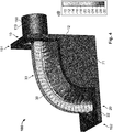
- Fig. 4 a visualization of a calculated distribution of the electric field in an embodiment of a redirecting device 100 is shown. It can be seen that only a small fraction of the field is present outside the waveguide member 30 so that the losses are low.
- a second fixing element 192 is similar to a first fixing element 91.
- FIG. 5 to 7 Several embodiments of a redirecting device 100 are shown in Figs. 5 to 7 .
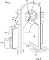
- the embodiment shown in Fig. 5 is similar to the one in Fig. 1 and comprises a rectangular cross-section 140 of the waveguide member 30. It further comprises a fixing element 191 next to the input section 10 for fixing the redirecting device 100 to the first external element 110.
- the first fixing section 191 comprises a plate-shaped structure that can provide stop faces for a positive fit with corresponding elements on the external element 10 or a plug 195 attached to the external element 110.
- Fixing can, for example, be achieved by further fixing elements 196 present at the sides of the redirecting device 100.
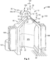
- This embodiment also has a rectangular cross-section 40.
- the parts 61 and 62 of the support structure 60 that extend away from the waveguide member 30 each take up only a small angle 67 around the waveguide member 30, preferably less than 30°, for example about 20°.
- the angle 67 is in this case measured around a center 45 of the waveguide member 30, that means that the center of the waveguide member 30 is taken as the vertex of the angle 67.
- the thickness 66 at the distance 180, 181 only makes up about 20% of the height 33 of the waveguide member 30.
- the waveguide member 30 has a circular cross-section. Again, in a cross-section, any part 61, 62 of the support structure 60 extending away from the waveguide member 30 makes up less than 10 degrees, preferably less than 5 degrees.
- FIGs. 8 to 10 several embodiments of an external element 150 that can be attached to the redirecting device 100 are shown.
- a first embodiment 151 which comprises a core 160 with a rectangular cross-section that is held in the center of a supporting ring 162 by support members 161.
- the second embodiment 152 shown in Fig. 9 comprises a core 160 with a square shaped cross-section, which is also held within a support ring 162 by support members 161.
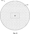
- a third embodiment 53 is shown in which a core 163 is located in the foam 169.
- the foam 169 has a low permittivity such that the waves are restrained within the core 160.
Landscapes
- Engineering & Computer Science (AREA)
- Microelectronics & Electronic Packaging (AREA)
- Waveguides (AREA)
- Waveguide Aerials (AREA)
Abstract
Description
- The invention relates to the area of redirecting mm-waves, that is, waves having a wavelength of 1 to 10 mm. Such waves are, for example, used in mobile communication (5G) or for radar signal transmission. For the transmission of such waves, flexible elements can be used. When such flexible elements are connected to other elements, for example a PCB, the assembly is very bulky.
- The object of the invention is thus to provide a solution that allows a more space saving connection.
- According to the invention, this object is achieved by a redirecting device for mm-waves, comprising an input section, an output section and a rigid, dielectric waveguide member extending from the input section to the output section, wherein the input section and the output section are at 90 degrees to each other.
- With this solution, flexible elements no longer have to be attached perpendicular to the other element, for example the PCB, but can rather be installed such that they run parallel to it. Such an arrangement is thus more space saving.
- A connection assembly comprises a redirecting device according to the invention.
- The solution according to the invention can further be improved by the following further developments and advantageous embodiments, which are independent of each other and can be combined arbitrarily, as desired.
- To improve the stability, the input section and the output section can be mechanically connected to each other. For example, they can be connected rigidly so that they cannot move relative to each other.
- The waveguide member can be a solid element. In contrast, for example, to a hollow waveguide member, a solid waveguide member can be manufactured more easily.
- In a simple design, the input section and/or the output section can comprise planar end surfaces of the waveguide member
- In order to achieve an easy coupling, the input section can comprise a first coupling face for coupling to a first external member and the waveguide member extends away from the first coupling face. The first coupling face can in particular be planar or flat to achieve a good coupling efficiency. The first external member can, in particular, be a cable or a flexible element like a dielectric waveguide. The waveguide member can preferably extend away perpendicularly from the first coupling face.
- Similarly, the output section can comprise a second coupling face for coupling to a second external member, and the waveguide member can extend away from the second coupling face .The second coupling face is also preferably planar and the waveguide member extends preferably perpendicularly away from the second coupling face. The second external member can be a PCB (printed circuit board). The PCB can, for example, comprise wave-emitting elements like an antenna.
- Preferably, the first and the second coupling face are 90 degrees to each other. This can simplify the coupling.
- In a simple design, the waveguide member can run along a 90 degree curve. The curve can have a constant radius to make the production simple. The waveguide member can comprise one or more curves with an angle different from 90 degrees, or straight sections.
- In order to avoid disturbances, the waveguide member can have a low or no elastic and plastic deformability. It can, for example, not be as flexible as a flexible element attached to it, for example a dielectric waveguide.
- For a good volume-to-length ratio, the waveguide member may be an elongated element. One dimension of the waveguide member can be larger than the other two dimensions by a factor of at least five. For example, the waveguide member can have a length that is larger than its width and/or height by a factor of at least five. The length can here be measured along a non-straight line, for example a curved line.
- The waveguide member may have a constant cross-section. This can result in good transmission characteristics. The cross-section, in particular the shape of the cross-section and the area of the cross-section, can be constant from the input section to the output section. The cross-section can be taken perpendicular to a length extension of the waveguide member. The cross-section in a plane comprising a width and a height can thus be constant along the length direction.
- The waveguide member can have various cross-sections. For example, a circular, an elliptical, or a rectangular shape are possible for transmitting different modes and orientations of the waves.
- In order to be adapted for the transmission of mm-waves, a dimension of the cross-section can be greater than 0.2 times the wavelength. and/or less than 1.5 times the wavelength. The wavelength can in particular relate to the wavelength that is to be transmitted.
- To minimize losses, the cross-section of the input section and/or the output section can be similar or identical to the cross-section of the waveguide member.
- Also to minimize losses, the cross-section of the waveguide member can be adapted to the cross-section of an attached waveguide, in particular the core of such a waveguide.
- To achieve a sufficient performance in the mm-range, a minimum curvature radius of the waveguide member can be greater than one wavelength.
- The waveguide member can, in particular, be curved in a plane that comprises a length direction.
- The redirecting device can comprise a planar sheet or board member located at or next to the input section and/or the output section. The board member can serve as a fixation element or a closure element when the redirecting device is attached to an external element. The board member can extend away from the input section or the output section to an extent that an open end of the attached external element is covered.
- In an advantageous embodiment, the redirecting device comprises a support structure for supporting the waveguide member.
- The support structure can extend along the waveguide member from the input section to the output section, preferably continuously and/or uninterruptedly.
- In one embodiment, the input section defines a first mounting plane and/or the output section defines a second mounting plane and the support structure extends from the waveguide member to the first mounting plane and/or the second mounting plane. This increases the stability of the waveguide member. The first mounting plane may be perpendicular to the second mounting plane.
- For improving the transmission performance, the support structure can enclose an air cladding and/or an air volume. Preferably, the air cladding and/or the air volume extends to the first mounting plane and/or the second mounting plane.
- In a lightweight embodiment having a good transmission performance, apart from the input section, the output section, and the support structure, no further material may be present next to the waveguide member. The expression "next to" can be understood as within 0.5 times the wavelength and/or a maximum width of waveguide member.
- In an alternative embodiment with a similarly good transmission performance, material with a low permittivity, e.g. foam, can be present next to the waveguide member. Such a material with a low permittivity can act as a spacer, ensuring that no material or elements with high permittivity can come close to the waveguide member and disturb the transmission performance.
- In a preferred embodiment, in which the transmission performance is improved, in a cross-section, the thickness of a part of the support structure extending away from the waveguide member is less than 20% of a maximum thickness of the waveguide member. The thickness can, for example, be measured at a distance of 0.5-times the wavelength away from the waveguide member. The thickness of this part can be measured in a circumferential direction. Preferably, the thickness of a part of the support structure extending away from the waveguide member is less than 10% of a maximum thickness of the waveguide member, especially 5%.
- Also for improving the transmission performance, in a cross-section, any part of the support structure extending away from the waveguide member can make up less than 30 degrees, preferably less than 20 degrees, more preferably less than 10 degrees. The angle can be measured at a distance of 1.0 times the wavelength away from the waveguide member taking the center of the waveguide member as the vertex of the angle. The sum of different angles of different parts in total can be less than 90 degrees, preferably less than 60 degrees, more preferably less than 45 degrees.
- The support structure can comprise a web, a strut, or a sheet-like element to maintain a low weight.
- To reduce the weight further while providing sufficient stability and improving the transmission performance, a part of the support structure extending away from the waveguide member can taper towards the waveguide member.
- In a preferred embodiment, the support structure comprises two parts extending away from the waveguide member and extending away from each other. This results in a good compromise between stability and weight. Preferably, the two parts extend away from each other at an angle. The angle can, for example, be 90 degrees or 60 degrees.
- A first part of the two parts can be connected to a first wall section and a second part of the two parts can be connected to a second wall section. The first wall section and the second wall section can run parallel to each other. They can extend up to the first mounting plane and/or the second mounting plane.
- For waveguide members with a rectangular cross section, a fixation point at which a part of the support structure is attached to the waveguide member should preferably be located at a corner of the rectangle, as the energy density there is low and the losses are thus minimal.
- In order to keep the weight down, the support structure can be arranged at an inner side of a curve of the waveguide member.
- The waveguide member and the support structure can be integral or one-piece in order to facilitate manufacturing.
- In a preferred embodiment, the redirecting device is configured to be moldable with a two-piece die. This simplifies the production. For example, a demolding direction can exist, along which no undercuts are present, such that the redirecting device can be removed from the two pieces of the die.
- In a further embodiment, the redirecting device is a single monolithic piece. This can make the production easy. Preferably, the redirecting device comprises only plastic, and no other materials like metal. Especially, the redirecting device can be a monolithically moulded piece.
- The connection assembly can further comprise a housing element, wherein the housing element is spaced at least 1.0 times the wavelength away from the waveguide member, at any point. This can improve the transmission performance as undesired coupling is avoided.
- The housing can be integral with the redirecting device. Both can be a single monolithic part.
- The invention will now be described in greater detail and in an exemplary manner using advantageous embodiments and with reference to the drawings. The described embodiments are only possible configurations in which, however, the individual features as described above can be provided independently of one another or can be omitted.
- In the Figs.:
- Fig. 1
- shows a schematic perspective view of a first embodiment of a redirecting device in a mounted state;
- Fig. 2
- shows a schematic perspective view of a second embodiment of a redirecting device;
- Fig. 3
- shows a schematic perspective view of the second embodiment of
Fig. 2 from a different viewpoint; - Fig. 4
- shows a schematic perspective view of a calculation of an e-field distribution in the second embodiment;
- Fig. 5
- shows a schematic perspective view of a third embodiment of a redirecting device;
- Fig. 6
- shows a schematic perspective view of a fourth embodiment of a redirecting device;
- Fig. 7
- shows a schematic perspective view of a fifth embodiment of a redirecting device;
- Fig. 8
- shows a schematic cross-sectional view of a sixth embodiment of a waveguide that can be attached to a redirecting device;
- Fig. 9
- shows a schematic cross-sectional view of a seventh embodiment of a waveguide that can be attached to a redirecting device;
- Fig. 10
- shows a schematic cross-sectional view of a third embodiment of a waveguide that can be attached to a redirecting device.
- In
Figs. 1 to 7 , several embodiments of a redirectingdevice 100 are shown. - In
Fig. 1 , a first embodiment of a redirectingdevice 100 is shown together with further components. The redirectingdevice 100 comprises aninput section 10 for connecting to a firstexternal element 110, which in this case is awaveguide 150. Electromagnetic waves of certain frequencies can pass through thewaveguide 150 and be directed to a secondexternal element 120 located atoutput section 20 at an opposite side of the redirectingdevice 100. The secondexternal element 120 is aPCB 121 in the depicted example. - For fixing the first
external element 110 to the redirectingdevice 100, aplug 195 can be used. For a good connection, the redirectingdevice 100 can comprise afirst fixing element 191. The redirectingdevice 100 further comprises asecond fixing element 192 for connecting to the secondexternal member 120. Thissecond fixing element 192 can, for example, comprise a through-hole through which a bolt or similar element can be inserted. - The redirecting
device 100 further comprises a rigid,dielectric waveguide member 30 extending from theinput section 10 to theoutput section 20. Thewaveguide member 30 serves to guide the electromagnetic waves from thewaveguide 150 to the element on thePCB 121 or from the element on thePCB 121 to thewaveguide 150. For example, mobile communication signals can be created on the element on thePCB 121 and then be directed to a distribution element further away. - The
input section 10 and theoutput section 20 are at 90 degrees to each other. This results in a space saving configuration, as thewaveguide 150 can be parallel to thePCB 121. - To stabilize the configuration, the
input section 10 andoutput section 20 are mechanically connected to each other. Thewaveguide member 30 has a low or no elastic and plastic deformability to improve the transmission performance. Thewaveguide member 30 can be a solid element. In contrast to a hollow element, such a solid element can be easier to produce. - The
waveguide member 30 is an elongated element. The dimension in alength direction 131 that goes along a curve from theinput section 10 to theoutput section 20 is greater by a factor of at least 5 than the dimensions in awidth direction 132 and aheight direction 133. Thelength direction 131, thewidth direction 132 and theheight direction 133 are each perpendicular to each other at a certain point of thewaveguide member 30. The absolute orientations of these directions however changes along the extension of thewaveguide member 30. - The
waveguide member 30 runs along a 90degree curve 33. In an easy embodiment, thecurve 33 could have a constant radius. However, the curvature radius can vary along thewaveguide member 30. Aminimum curvature radius 36 should not be below a certain limit in order to be able to appropriately transmit the mm-waves, which have wavelengths of approximately 1 to 10 mm in vacuum. - The redirecting
device 100 comprises asupport structure 60 for supporting thewaveguide member 30. Thesupport structure 60 extends along thewaveguide member 30 from theinput section 10 to theoutput section 20. In the depicted example, thesupport structure 60 extends continuously or uninterruptedly from theinput section 10 to theoutput section 20. However, in an embodiment that is more lightweight, holes or recesses could be present in the material. Thesupport structure 60 can comprise webs, struts and/or sheet-like sections. Thesupport structure 60 can comprise or contain basically flat sections to keep the weight low. - The
support structure 60 is arranged at aninner side 35 of thecurve 33 of thewaveguide member 30, in order to save space. - In
Figs. 2 and3 , further details of an embodiment of the redirectingdevice 100 can be seen. - The
input section 10 and theoutput section 20 comprise planar end surfaces 31, 32 of thewaveguide member 30, which constitute afirst coupling face 11 for coupling to the firstexternal member 110 and asecond coupling face 21 for coupling to the secondexternal member 120. - The
waveguide member 30 extends away in a perpendicular manner from thefirst coupling face 11 and thesecond coupling face 21. The first coupling face 7 and thesecond coupling face 21 are 90 degrees to each other. The first coupling face 7 and thesecond coupling face 21 are configured to be in direct contact with further external elements, like thewaveguide 150 and the element on thePCB 121. - The
waveguide member 30 has aconstant cross-section 140 from theinput section 10 to theoutput section 20. Thus, thecross-section 140 of theinput section 10 and theoutput section 20 are similar, in particular identical, to thecross-section 140 of thewaveguide member 30. - In the embodiment shown in
Figs. 2 and3 , thecross section 140 is rectangular. In other embodiments, thecross section 140 can have other shapes and, for example, be circular or elliptical. In order to achieve a good transmission, a dimension of thecross-section 140 should be within a certain range defined by the waves used with the redirectingdevice 100. Further, thecross-section 140 can be adapted to thewaveguide 150, in particular to the cross-section of the core of thewaveguide 150. - In order to minimize losses, fixation points 55, at which the
support structure 60 is attached to thewaveguide member 30, are located atcorners 52 of therectangular cross-section 140. - The
input section 10 defines a first mountingplane 12 and theoutput section 20 defines a second mountingplane 22. Thefirst coupling face 11 and thesecond coupling face 21 are flush with the first mountingplane 12 or the second mountingplane 22, respectively. - The
support structure 60 extends from thewaveguide member 30 to the first mountingplane 12, and the second mountingplane 22. The first mountingplane 12 is perpendicular to the second mountingplane 22. - The
support structure 60 encloses an air volume or anair cladding 170. The fact that no material is present in this area results in a good transmission of the waves. In the depicted example, theair cladding 170 extends to the second mountingplane 22. In further embodiments, theair cladding 170 can also extend to the first mountingplane 12. - To avoid outcoupling of signals, and thus improve the signal, apart from the
input section 10, theoutput section 20, and thesupport structure 60, no further material is present next to the waveguide member 30 (that means within acertain distance 183 from the waveguide member 30). Thedistance 183 can be dependent on the wavelength that is used. In alternative embodiments, a material with a low permittivity, e.g. foam, can be present next to thewaveguide member 30 for achieving a similar effect. - The
support structure 60 comprises twoparts waveguide member 30 and extending away from each other at anangle 69. - A
first part 61 is connected to afirst wall section 71 and asecond part 62 is connected to asecond wall section 22. Thefirst wall section 71 and thesecond wall section 72 run parallel to each other. - As can, for example, be seen in
Fig. 3 , in a cross-section, thethickness 66 of thepart 61 of thesupport structure 60 extending away from thewaveguide member 30 is less than 20% of amaximum thickness 37 of thewaveguide member 30. Themaximum thickness 37 can, in this example, be theheight 43 of thewaveguide member 30 measured in aheight direction 133. It could also be thewidth 42 or a radius. - The
thickness 66 can be measured at adistance 180 away from a center of thewaveguide member 30. It could also be measured from the outer surface of thewaveguide member 30. Thedistance 180 can, for example, be defined by multiples of the wavelength. Thethickness 66 can also be the thickness of thepart waveguide member 30. Thethickness 66 of thefirst part 61 is measured in a circumferential direction. Thethickness 66 of thefirst part 61 is also similar to the thickness of thesecond part 62 of thesupport structure 60 and to the thickness of further support elements present at theinput section 10 or theoutput section 20. - Each of the
parts support structure 60 extending away from thewaveguide member 30 tapers towards thewaveguide member 30, which means its thickness decreases towards thewaveguide member 30. - The
support structure 60 is arranged at aninner side 35 of thecurve 33 of thewaveguide member 30. - The redirecting
device 100 is a single monolithic piece. It comprises only plastic, no metal, not even as a coating. This can simplify the production. - Embodiments of the redirecting
device 100 can be configured to be moldable with a two-piece die. For example, a deformation direction can exist along which no undercuts are present. The redirectingdevice 100 can be a monolithically molded piece. - The
first fixation element 191 is formed by a board member 185 of the redirectingdevice 100. The board member 185 is a planar sheet like section of the redirectingdevice 100 that is in the present case located next to theinput section 10. A further board member 185 can be present at theoutput section 20. The board member 185 can serve to cover or close off attached external elements to avoid damages. The board member 185 extends away from theinput section 10 sideways, towards the second mountingplane 22 and away from the second mountingplane 22. - A
connection assembly 200 comprises a redirectingdevice 100 and can further comprise a housing element 190, wherein the housing element 190 is spaced a certain distance away from thewaveguide member 30. The housing element 190 is, for example, shown schematically only in broken lines inFig. 2 . - In
Fig. 4 , a visualization of a calculated distribution of the electric field in an embodiment of a redirectingdevice 100 is shown. It can be seen that only a small fraction of the field is present outside thewaveguide member 30 so that the losses are low. - Further, a
second fixing element 192 is similar to a first fixing element 91. - Several embodiments of a redirecting
device 100 are shown inFigs. 5 to 7 . - The embodiment shown in
Fig. 5 is similar to the one inFig. 1 and comprises arectangular cross-section 140 of thewaveguide member 30. It further comprises a fixingelement 191 next to theinput section 10 for fixing the redirectingdevice 100 to the firstexternal element 110. Thefirst fixing section 191 comprises a plate-shaped structure that can provide stop faces for a positive fit with corresponding elements on theexternal element 10 or aplug 195 attached to theexternal element 110. - In the embodiment shown in
Fig. 6 , no such plate-shaped structure is present. Fixing can, for example, be achieved by further fixingelements 196 present at the sides of the redirectingdevice 100. This embodiment also has a rectangular cross-section 40. - It can further be seen that at a
distance 181 away from the center of thewaveguide member 30, theparts support structure 60 that extend away from thewaveguide member 30 each take up only asmall angle 67 around thewaveguide member 30, preferably less than 30°, for example about 20°. Theangle 67 is in this case measured around acenter 45 of thewaveguide member 30, that means that the center of thewaveguide member 30 is taken as the vertex of theangle 67. Further, thethickness 66 at thedistance height 33 of thewaveguide member 30. - In the embodiment shown in
Fig. 7 , thewaveguide member 30 has a circular cross-section. Again, in a cross-section, anypart support structure 60 extending away from thewaveguide member 30 makes up less than 10 degrees, preferably less than 5 degrees. - In
Figs. 8 to 10 , several embodiments of anexternal element 150 that can be attached to the redirectingdevice 100 are shown. - In
Fig. 8 , afirst embodiment 151 is shown, which comprises a core 160 with a rectangular cross-section that is held in the center of a supportingring 162 bysupport members 161. - The
second embodiment 152 shown inFig. 9 comprises a core 160 with a square shaped cross-section, which is also held within asupport ring 162 bysupport members 161. - In
Fig. 10 , a third embodiment 53 is shown in which a core 163 is located in thefoam 169. Thefoam 169 has a low permittivity such that the waves are restrained within thecore 160. -
- 10
- input section
- 11
- coupling face
- 12
- first mounting plane
- 20
- output section
- 21
- coupling face
- 22
- second mounting plane
- 30
- waveguide member
- 31
- end surface
- 32
- end surface
- 33
- curve
- 34
- radius of curve
- 35
- inner side of curve
- 36
- minimum curvature radius
- 37
- thickness
- 39
- elongated element
- 41
- length of waveguide member
- 42
- width of waveguide member
- 43
- height of waveguide member
- 45
- center of waveguide member
- 50
- cross section
- 51
- rectangle
- 52
- corner
- 60
- support structure
- 61
- first part
- 62
- second part
- 66
- thickness part
- 67
- angle part
- 69
- angle first part - second part
- 71
- first wall section
- 72
- second wall section
- 100
- redirecting device
- 110
- first external member
- 120
- second external member
- 121
- PCB
- 131
- length direction
- 132
- width direction
- 133
- height direction
- 140
- cross section
- 150
- waveguide
- 151
- first embodiment of a waveguide
- 152
- second embodiment of a waveguide
- 153
- third embodiment of a waveguide
- 160
- core
- 161
- support member
- 169
- foam
- 170
- air cladding
- 180
- distance
- 181
- distance
- 183
- distance
- 185
- board member
- 190
- housing
- 191
- fixing element
- 192
- fixing element
- 195
- plug
- 196
- fixing element
- 200
- connector assembly
Claims (15)
- Redirecting device (100) for mm-waves, comprising an input section (10), an output section (20), and a rigid, dielectric waveguide member (30) extending from the input section (10) to the output section (20), wherein the input section (10) and the output section (20) are at 90 degrees to each other.
- Redirecting device (100) according to claim 1, wherein the waveguide member (30) is an elongated element.
- Redirecting device (100) according to claim 1 or 2, wherein the waveguide member (30) has a constant cross-section (140).
- Redirecting device (100) according to one of claims 1 to 3, wherein a minimum curvature radius (36) of the waveguide member (30) is greater than one wavelength
- Redirecting device (100) according to one of claims 1 to 4, wherein the redirecting device (100) comprises a support structure (60) for supporting the waveguide member (30).
- Redirecting device (100) according to claim 5, wherein the support structure (60) extends along the waveguide member (30) from the input section (10) to the output section (20).
- Redirecting device (100) according to one of claim 5 or 6, wherein the input section (10) defines a first mounting plane (12) and/or the output section (20) defines a second mounting plane (22) and the support structure (60) extends from the waveguide member (30) to the first mounting plane (12) and/or the second mounting plane (22).
- Redirecting device (100) according to one of claims 5 to 7, wherein the support structure (60) encloses an air cladding (170).
- Redirecting device (100) according to one of claims 5 to 8, wherein apart from the input section (10), the output section (20) and the support structure (60) no further material is present next to the waveguide member (30).
- Redirecting device (100) according to one of claims 5 to 9, wherein in a cross-section the thickness (66) of a part (61, 62) of the support structure (60) extending away from the waveguide member (30) is less than 20 % of a maximum thickness (37) of the waveguide member (30).
- Redirecting device (100) according to one of claims 5 to 10, wherein in a cross-section any part (61, 62) of the support structure (60) extending away from the waveguide member (30) makes up less than 10 degrees, preferably less than 5 degrees.
- Redirecting device (100) according to one of claims 5 to 11, wherein a part (61, 62) of the support structure (60) extending away from the waveguide member (30) tapers towards the waveguide member (30) .
- Redirecting device (100) according to one of claims 5 to 12, wherein the support structure (60) is arranged at an inner side (35) of a curve (33) of the waveguide member (30).
- Redirecting device (100) according to one of claims 1 to 13, wherein the redirecting device (100) is a single monolithic piece.
- Connection assembly (200) comprising a redirecting device according to any one of claims 1 to 14, further comprising a housing element (190), wherein the housing element (190) is spaced at least z times the wavelength away from the waveguide member (100).
Priority Applications (2)
| Application Number | Priority Date | Filing Date | Title |
|---|---|---|---|
| EP19194690.4A EP3787100B1 (en) | 2019-08-30 | 2019-08-30 | Redirecting device for mm-waves, connection assembly |
| US17/005,717 US11664562B2 (en) | 2019-08-30 | 2020-08-28 | Redirecting device for mm-waves, connection assembly |
Applications Claiming Priority (1)
| Application Number | Priority Date | Filing Date | Title |
|---|---|---|---|
| EP19194690.4A EP3787100B1 (en) | 2019-08-30 | 2019-08-30 | Redirecting device for mm-waves, connection assembly |
Publications (2)
| Publication Number | Publication Date |
|---|---|
| EP3787100A1 true EP3787100A1 (en) | 2021-03-03 |
| EP3787100B1 EP3787100B1 (en) | 2025-04-23 |
Family
ID=67810519
Family Applications (1)
| Application Number | Title | Priority Date | Filing Date |
|---|---|---|---|
| EP19194690.4A Active EP3787100B1 (en) | 2019-08-30 | 2019-08-30 | Redirecting device for mm-waves, connection assembly |
Country Status (2)
| Country | Link |
|---|---|
| US (1) | US11664562B2 (en) |
| EP (1) | EP3787100B1 (en) |
Citations (5)
| Publication number | Priority date | Publication date | Assignee | Title |
|---|---|---|---|---|
| EP0767507A1 (en) * | 1995-10-04 | 1997-04-09 | Murata Manufacturing Co., Ltd. | Dielectric waveguide |
| WO2014099389A1 (en) * | 2012-12-20 | 2014-06-26 | 3M Innovative Properties Company | Floating connector shield |
| US20140285277A1 (en) * | 2013-03-19 | 2014-09-25 | Texas Instruments Incorporated | Dielectric Waveguide Manufactured Using Printed Circuit Board Technology |
| US20170170539A1 (en) * | 2015-12-14 | 2017-06-15 | Tyco Electronics Corporation | Dielectric waveguide |
| EP3462533A1 (en) * | 2017-09-28 | 2019-04-03 | TE Connectivity Germany GmbH | Low-loss plug connection arrangement and system having at least one such plug connection arrangement |
Family Cites Families (4)
| Publication number | Priority date | Publication date | Assignee | Title |
|---|---|---|---|---|
| DE60208244T2 (en) * | 2001-01-12 | 2006-06-29 | Murata Manufacturing Co., Ltd., Nagaokakyo | Transmission line arrangement, integrated circuit and transmitter-receiver device |
| JP6414632B2 (en) * | 2015-03-31 | 2018-10-31 | ダイキン工業株式会社 | Dielectric waveguide line |
| US10249925B2 (en) * | 2016-09-30 | 2019-04-02 | Intel Corporation | Dielectric waveguide bundle including a supporting feature for connecting first and second server boards |
| US20180198184A1 (en) * | 2017-01-11 | 2018-07-12 | Sumitomo Electric Industries, Ltd. | Cable for transmitting electromagnetic waves |
-
2019
- 2019-08-30 EP EP19194690.4A patent/EP3787100B1/en active Active
-
2020
- 2020-08-28 US US17/005,717 patent/US11664562B2/en active Active
Patent Citations (5)
| Publication number | Priority date | Publication date | Assignee | Title |
|---|---|---|---|---|
| EP0767507A1 (en) * | 1995-10-04 | 1997-04-09 | Murata Manufacturing Co., Ltd. | Dielectric waveguide |
| WO2014099389A1 (en) * | 2012-12-20 | 2014-06-26 | 3M Innovative Properties Company | Floating connector shield |
| US20140285277A1 (en) * | 2013-03-19 | 2014-09-25 | Texas Instruments Incorporated | Dielectric Waveguide Manufactured Using Printed Circuit Board Technology |
| US20170170539A1 (en) * | 2015-12-14 | 2017-06-15 | Tyco Electronics Corporation | Dielectric waveguide |
| EP3462533A1 (en) * | 2017-09-28 | 2019-04-03 | TE Connectivity Germany GmbH | Low-loss plug connection arrangement and system having at least one such plug connection arrangement |
Also Published As
| Publication number | Publication date |
|---|---|
| US11664562B2 (en) | 2023-05-30 |
| EP3787100B1 (en) | 2025-04-23 |
| US20210066776A1 (en) | 2021-03-04 |
Similar Documents
| Publication | Publication Date | Title |
|---|---|---|
| US6809691B2 (en) | Directivity controllable antenna and antenna unit using the same | |
| US10658761B2 (en) | Adapter structure with waveguide channels | |
| US8188805B2 (en) | Triplate line-to-waveguide transducer having spacer dimensions which are larger than waveguide dimensions | |
| JP4803172B2 (en) | Planar antenna module, triplate type planar array antenna, and triplate line-waveguide converter | |
| CN210015951U (en) | Active antenna unit and shell thereof | |
| CN113097743B (en) | Single-layer realizable high-aperture-efficiency parallel-fed waveguide slot array antenna | |
| EP0985243A1 (en) | Microwave transmission device | |
| KR102136445B1 (en) | System for feeding high-frequency waves to deployment structure | |
| US8570120B2 (en) | Heat insulating waveguides separated by an air gap and including two planar reflectors for controlling radiation power from the air gap | |
| JP2005045341A (en) | Waveguide anti-reflection terminator and waveguide circuit | |
| WO2023143003A1 (en) | A dielectric filter | |
| CN208423180U (en) | A kind of cavity feeding network and antenna inhibiting resonance | |
| JP2014007456A (en) | Coaxial waveguide converter and manufacturing method therefor | |
| EP3787100B1 (en) | Redirecting device for mm-waves, connection assembly | |
| US12341250B1 (en) | Offset-fed reflector parallel plate antenna apparatus | |
| JP2005020077A (en) | 90 degree bent waveguide, waveguide filter element, and high frequency circuit unit | |
| KR101468409B1 (en) | Dual mode resonator including the disk with notch and filter using the same | |
| CN220400903U (en) | A Yagi antenna and communication equipment | |
| KR20020035593A (en) | Dielectric resonator device, filter, duplexer, and communication device | |
| JP2020022075A (en) | Transducer | |
| JP7240277B2 (en) | Waveguide antenna and antenna device | |
| CN115441167A (en) | Compact Low Profile Aperture Antenna with Integrated Diplexer | |
| CN218275033U (en) | Antenna assembly, wireless communication relay device, and electronic apparatus | |
| KR19990084408A (en) | Planar antenna using multilayer dielectric with air layer | |
| CN215771497U (en) | Microwave broadband cavity coupler |
Legal Events
| Date | Code | Title | Description |
|---|---|---|---|
| PUAI | Public reference made under article 153(3) epc to a published international application that has entered the european phase |
Free format text: ORIGINAL CODE: 0009012 |
|
| STAA | Information on the status of an ep patent application or granted ep patent |
Free format text: STATUS: THE APPLICATION HAS BEEN PUBLISHED |
|
| AK | Designated contracting states |
Kind code of ref document: A1 Designated state(s): AL AT BE BG CH CY CZ DE DK EE ES FI FR GB GR HR HU IE IS IT LI LT LU LV MC MK MT NL NO PL PT RO RS SE SI SK SM TR |
|
| AX | Request for extension of the european patent |
Extension state: BA ME |
|
| STAA | Information on the status of an ep patent application or granted ep patent |
Free format text: STATUS: REQUEST FOR EXAMINATION WAS MADE |
|
| 17P | Request for examination filed |
Effective date: 20210825 |
|
| RBV | Designated contracting states (corrected) |
Designated state(s): AL AT BE BG CH CY CZ DE DK EE ES FI FR GB GR HR HU IE IS IT LI LT LU LV MC MK MT NL NO PL PT RO RS SE SI SK SM TR |
|
| STAA | Information on the status of an ep patent application or granted ep patent |
Free format text: STATUS: EXAMINATION IS IN PROGRESS |
|
| 17Q | First examination report despatched |
Effective date: 20230523 |
|
| GRAP | Despatch of communication of intention to grant a patent |
Free format text: ORIGINAL CODE: EPIDOSNIGR1 |
|
| STAA | Information on the status of an ep patent application or granted ep patent |
Free format text: STATUS: GRANT OF PATENT IS INTENDED |
|
| INTG | Intention to grant announced |
Effective date: 20241213 |
|
| GRAS | Grant fee paid |
Free format text: ORIGINAL CODE: EPIDOSNIGR3 |
|
| GRAA | (expected) grant |
Free format text: ORIGINAL CODE: 0009210 |
|
| STAA | Information on the status of an ep patent application or granted ep patent |
Free format text: STATUS: THE PATENT HAS BEEN GRANTED |
|
| AK | Designated contracting states |
Kind code of ref document: B1 Designated state(s): AL AT BE BG CH CY CZ DE DK EE ES FI FR GB GR HR HU IE IS IT LI LT LU LV MC MK MT NL NO PL PT RO RS SE SI SK SM TR |
|
| REG | Reference to a national code |
Ref country code: GB Ref legal event code: FG4D |
|
| REG | Reference to a national code |
Ref country code: CH Ref legal event code: EP |
|
| REG | Reference to a national code |
Ref country code: DE Ref legal event code: R096 Ref document number: 602019068933 Country of ref document: DE |
|
| REG | Reference to a national code |
Ref country code: IE Ref legal event code: FG4D |
|
| REG | Reference to a national code |
Ref country code: NL Ref legal event code: MP Effective date: 20250423 |
|
| PG25 | Lapsed in a contracting state [announced via postgrant information from national office to epo] |
Ref country code: NL Free format text: LAPSE BECAUSE OF FAILURE TO SUBMIT A TRANSLATION OF THE DESCRIPTION OR TO PAY THE FEE WITHIN THE PRESCRIBED TIME-LIMIT Effective date: 20250423 |
|
| REG | Reference to a national code |
Ref country code: AT Ref legal event code: MK05 Ref document number: 1788734 Country of ref document: AT Kind code of ref document: T Effective date: 20250423 |
|
| PG25 | Lapsed in a contracting state [announced via postgrant information from national office to epo] |
Ref country code: PT Free format text: LAPSE BECAUSE OF FAILURE TO SUBMIT A TRANSLATION OF THE DESCRIPTION OR TO PAY THE FEE WITHIN THE PRESCRIBED TIME-LIMIT Effective date: 20250825 Ref country code: FI Free format text: LAPSE BECAUSE OF FAILURE TO SUBMIT A TRANSLATION OF THE DESCRIPTION OR TO PAY THE FEE WITHIN THE PRESCRIBED TIME-LIMIT Effective date: 20250423 Ref country code: ES Free format text: LAPSE BECAUSE OF FAILURE TO SUBMIT A TRANSLATION OF THE DESCRIPTION OR TO PAY THE FEE WITHIN THE PRESCRIBED TIME-LIMIT Effective date: 20250423 |
|
| PGFP | Annual fee paid to national office [announced via postgrant information from national office to epo] |
Ref country code: DE Payment date: 20250702 Year of fee payment: 7 |
|
| REG | Reference to a national code |
Ref country code: LT Ref legal event code: MG9D |
|
| PG25 | Lapsed in a contracting state [announced via postgrant information from national office to epo] |
Ref country code: GR Free format text: LAPSE BECAUSE OF FAILURE TO SUBMIT A TRANSLATION OF THE DESCRIPTION OR TO PAY THE FEE WITHIN THE PRESCRIBED TIME-LIMIT Effective date: 20250724 Ref country code: NO Free format text: LAPSE BECAUSE OF FAILURE TO SUBMIT A TRANSLATION OF THE DESCRIPTION OR TO PAY THE FEE WITHIN THE PRESCRIBED TIME-LIMIT Effective date: 20250723 |
|
| PG25 | Lapsed in a contracting state [announced via postgrant information from national office to epo] |
Ref country code: PL Free format text: LAPSE BECAUSE OF FAILURE TO SUBMIT A TRANSLATION OF THE DESCRIPTION OR TO PAY THE FEE WITHIN THE PRESCRIBED TIME-LIMIT Effective date: 20250423 |
|
| PG25 | Lapsed in a contracting state [announced via postgrant information from national office to epo] |
Ref country code: BG Free format text: LAPSE BECAUSE OF FAILURE TO SUBMIT A TRANSLATION OF THE DESCRIPTION OR TO PAY THE FEE WITHIN THE PRESCRIBED TIME-LIMIT Effective date: 20250423 |
|
| PG25 | Lapsed in a contracting state [announced via postgrant information from national office to epo] |
Ref country code: HR Free format text: LAPSE BECAUSE OF FAILURE TO SUBMIT A TRANSLATION OF THE DESCRIPTION OR TO PAY THE FEE WITHIN THE PRESCRIBED TIME-LIMIT Effective date: 20250423 |
|
| PG25 | Lapsed in a contracting state [announced via postgrant information from national office to epo] |
Ref country code: AT Free format text: LAPSE BECAUSE OF FAILURE TO SUBMIT A TRANSLATION OF THE DESCRIPTION OR TO PAY THE FEE WITHIN THE PRESCRIBED TIME-LIMIT Effective date: 20250423 |
|
| PG25 | Lapsed in a contracting state [announced via postgrant information from national office to epo] |
Ref country code: RS Free format text: LAPSE BECAUSE OF FAILURE TO SUBMIT A TRANSLATION OF THE DESCRIPTION OR TO PAY THE FEE WITHIN THE PRESCRIBED TIME-LIMIT Effective date: 20250723 |
|
| PG25 | Lapsed in a contracting state [announced via postgrant information from national office to epo] |
Ref country code: IS Free format text: LAPSE BECAUSE OF FAILURE TO SUBMIT A TRANSLATION OF THE DESCRIPTION OR TO PAY THE FEE WITHIN THE PRESCRIBED TIME-LIMIT Effective date: 20250823 |
|
| PG25 | Lapsed in a contracting state [announced via postgrant information from national office to epo] |
Ref country code: LV Free format text: LAPSE BECAUSE OF FAILURE TO SUBMIT A TRANSLATION OF THE DESCRIPTION OR TO PAY THE FEE WITHIN THE PRESCRIBED TIME-LIMIT Effective date: 20250423 |
|
| PG25 | Lapsed in a contracting state [announced via postgrant information from national office to epo] |
Ref country code: DK Free format text: LAPSE BECAUSE OF FAILURE TO SUBMIT A TRANSLATION OF THE DESCRIPTION OR TO PAY THE FEE WITHIN THE PRESCRIBED TIME-LIMIT Effective date: 20250423 Ref country code: SM Free format text: LAPSE BECAUSE OF FAILURE TO SUBMIT A TRANSLATION OF THE DESCRIPTION OR TO PAY THE FEE WITHIN THE PRESCRIBED TIME-LIMIT Effective date: 20250423 |
|
| PG25 | Lapsed in a contracting state [announced via postgrant information from national office to epo] |
Ref country code: CZ Free format text: LAPSE BECAUSE OF FAILURE TO SUBMIT A TRANSLATION OF THE DESCRIPTION OR TO PAY THE FEE WITHIN THE PRESCRIBED TIME-LIMIT Effective date: 20250423 |
|
| PG25 | Lapsed in a contracting state [announced via postgrant information from national office to epo] |
Ref country code: EE Free format text: LAPSE BECAUSE OF FAILURE TO SUBMIT A TRANSLATION OF THE DESCRIPTION OR TO PAY THE FEE WITHIN THE PRESCRIBED TIME-LIMIT Effective date: 20250423 |
|
| REG | Reference to a national code |
Ref country code: DE Ref legal event code: R097 Ref document number: 602019068933 Country of ref document: DE |
|
| PG25 | Lapsed in a contracting state [announced via postgrant information from national office to epo] |
Ref country code: RO Free format text: LAPSE BECAUSE OF FAILURE TO SUBMIT A TRANSLATION OF THE DESCRIPTION OR TO PAY THE FEE WITHIN THE PRESCRIBED TIME-LIMIT Effective date: 20250423 Ref country code: SK Free format text: LAPSE BECAUSE OF FAILURE TO SUBMIT A TRANSLATION OF THE DESCRIPTION OR TO PAY THE FEE WITHIN THE PRESCRIBED TIME-LIMIT Effective date: 20250423 |
|
| PG25 | Lapsed in a contracting state [announced via postgrant information from national office to epo] |
Ref country code: IT Free format text: LAPSE BECAUSE OF FAILURE TO SUBMIT A TRANSLATION OF THE DESCRIPTION OR TO PAY THE FEE WITHIN THE PRESCRIBED TIME-LIMIT Effective date: 20250423 |
|
| PLBE | No opposition filed within time limit |
Free format text: ORIGINAL CODE: 0009261 |
|
| STAA | Information on the status of an ep patent application or granted ep patent |
Free format text: STATUS: NO OPPOSITION FILED WITHIN TIME LIMIT |
|
| REG | Reference to a national code |
Ref country code: CH Ref legal event code: L10 Free format text: ST27 STATUS EVENT CODE: U-0-0-L10-L00 (AS PROVIDED BY THE NATIONAL OFFICE) Effective date: 20260304 |
|
| REG | Reference to a national code |
Ref country code: CH Ref legal event code: H13 Free format text: ST27 STATUS EVENT CODE: U-0-0-H10-H13 (AS PROVIDED BY THE NATIONAL OFFICE) Effective date: 20260324 |
|
| PG25 | Lapsed in a contracting state [announced via postgrant information from national office to epo] |
Ref country code: MC Free format text: LAPSE BECAUSE OF FAILURE TO SUBMIT A TRANSLATION OF THE DESCRIPTION OR TO PAY THE FEE WITHIN THE PRESCRIBED TIME-LIMIT Effective date: 20250423 |
|
| 26N | No opposition filed |
Effective date: 20260126 |
|
| PG25 | Lapsed in a contracting state [announced via postgrant information from national office to epo] |
Ref country code: LU Free format text: LAPSE BECAUSE OF NON-PAYMENT OF DUE FEES Effective date: 20250830 |
|
| PG25 | Lapsed in a contracting state [announced via postgrant information from national office to epo] |
Ref country code: CH Free format text: LAPSE BECAUSE OF NON-PAYMENT OF DUE FEES Effective date: 20250831 |
|
| GBPC | Gb: european patent ceased through non-payment of renewal fee |
Effective date: 20250830 |
|
| REG | Reference to a national code |
Ref country code: BE Ref legal event code: MM Effective date: 20250831 |
|
| PG25 | Lapsed in a contracting state [announced via postgrant information from national office to epo] |
Ref country code: LT Free format text: LAPSE BECAUSE OF FAILURE TO SUBMIT A TRANSLATION OF THE DESCRIPTION OR TO PAY THE FEE WITHIN THE PRESCRIBED TIME-LIMIT Effective date: 20250423 |
|
| PG25 | Lapsed in a contracting state [announced via postgrant information from national office to epo] |
Ref country code: GB Free format text: LAPSE BECAUSE OF NON-PAYMENT OF DUE FEES Effective date: 20250830 |
|
| PG25 | Lapsed in a contracting state [announced via postgrant information from national office to epo] |
Ref country code: BE Free format text: LAPSE BECAUSE OF NON-PAYMENT OF DUE FEES Effective date: 20250831 Ref country code: IE Free format text: LAPSE BECAUSE OF NON-PAYMENT OF DUE FEES Effective date: 20250830 |
|
| PG25 | Lapsed in a contracting state [announced via postgrant information from national office to epo] |
Ref country code: FR Free format text: LAPSE BECAUSE OF NON-PAYMENT OF DUE FEES Effective date: 20250831 |
|
| PG25 | Lapsed in a contracting state [announced via postgrant information from national office to epo] |
Ref country code: SE Free format text: LAPSE BECAUSE OF FAILURE TO SUBMIT A TRANSLATION OF THE DESCRIPTION OR TO PAY THE FEE WITHIN THE PRESCRIBED TIME-LIMIT Effective date: 20250423 |