EP3786957A1 - Tunnel magnetoresistance (tmr) element having cobalt iron and tantalum layers - Google Patents
Tunnel magnetoresistance (tmr) element having cobalt iron and tantalum layers Download PDFInfo
- Publication number
- EP3786957A1 EP3786957A1 EP20192931.2A EP20192931A EP3786957A1 EP 3786957 A1 EP3786957 A1 EP 3786957A1 EP 20192931 A EP20192931 A EP 20192931A EP 3786957 A1 EP3786957 A1 EP 3786957A1
- Authority
- EP
- European Patent Office
- Prior art keywords
- layer
- tmr
- cofeb
- cofe
- tantalum
- Prior art date
- Legal status (The legal status is an assumption and is not a legal conclusion. Google has not performed a legal analysis and makes no representation as to the accuracy of the status listed.)
- Granted
Links
Images



Classifications
-
- G—PHYSICS
- G11—INFORMATION STORAGE
- G11C—STATIC STORES
- G11C11/00—Digital stores characterised by the use of particular electric or magnetic storage elements; Storage elements therefor
- G11C11/02—Digital stores characterised by the use of particular electric or magnetic storage elements; Storage elements therefor using magnetic elements
- G11C11/16—Digital stores characterised by the use of particular electric or magnetic storage elements; Storage elements therefor using magnetic elements using elements in which the storage effect is based on magnetic spin effect
- G11C11/161—Digital stores characterised by the use of particular electric or magnetic storage elements; Storage elements therefor using magnetic elements using elements in which the storage effect is based on magnetic spin effect details concerning the memory cell structure, e.g. the layers of the ferromagnetic memory cell
-
- H—ELECTRICITY
- H01—ELECTRIC ELEMENTS
- H01F—MAGNETS; INDUCTANCES; TRANSFORMERS; SELECTION OF MATERIALS FOR THEIR MAGNETIC PROPERTIES
- H01F10/00—Thin magnetic films, e.g. of one-domain structure
- H01F10/32—Spin-exchange-coupled multilayers, e.g. nanostructured superlattices
- H01F10/324—Exchange coupling of magnetic film pairs via a very thin non-magnetic spacer, e.g. by exchange with conduction electrons of the spacer
- H01F10/3254—Exchange coupling of magnetic film pairs via a very thin non-magnetic spacer, e.g. by exchange with conduction electrons of the spacer the spacer being semiconducting or insulating, e.g. for spin tunnel junction [STJ]
-
- H—ELECTRICITY
- H10—SEMICONDUCTOR DEVICES; ELECTRIC SOLID-STATE DEVICES NOT OTHERWISE PROVIDED FOR
- H10N—ELECTRIC SOLID-STATE DEVICES NOT OTHERWISE PROVIDED FOR
- H10N50/00—Galvanomagnetic devices
- H10N50/10—Magnetoresistive devices
-
- H—ELECTRICITY
- H10—SEMICONDUCTOR DEVICES; ELECTRIC SOLID-STATE DEVICES NOT OTHERWISE PROVIDED FOR
- H10N—ELECTRIC SOLID-STATE DEVICES NOT OTHERWISE PROVIDED FOR
- H10N50/00—Galvanomagnetic devices
- H10N50/80—Constructional details
- H10N50/85—Materials of the active region
Definitions
- MgO Magnesium oxide
- MTJs magnetic tunnel junctions
- MR% magneto-resistance ratio
- the reason for this high ratio is due to the so-called coherent tunneling mechanism through the MgO barrier which filters in only highly-spin polarized electronic states.
- GMR giant magnetoresistance
- MTJs When compared with similar giant magnetoresistance (GMR) structures, MTJs generally show lower reference stability (lower spin flop field) and higher free layer anisotropy (higher coercivity).
- a tunnel magnetoresistance (TMR) element in one aspect, includes a magnesium oxide (MgO) layer, a first cobalt iron boron (CoFeB) layer in direct contact with the MgO layer and a first cobalt iron (CoFe) layer.
- the TMR element also includes a first tantalum layer in direct contact with the first CoFeB layer and the first CoFe layer.
- the aspect above may include one or more of the following features.
- the first CoFeB layer, the first CoFe layer and the first tantalum layer may be part of a reference layer.
- the first CoFeB layer may be about 0.9 nanometers thick.
- the first CoFe layer may be about 0.9 nanometers thick.
- the first tantalum layer may be about 0.1 nanometers thick.
- a thickness of the first tantalum layer may be between 0.05 nanometers and 0.3 nanometers.
- the first CoFeB layer, the first CoFe layer and the first tantalum layer may be part of a free layer.
- the free layer may include a nickel iron (NiFe) layer and the NiFe layer may be in direct contact with the first CoFe layer.
- the first CoFeB layer may be about 1.0 nanometer thick.
- the first CoFe layer may be about 1.0 nanometer thick.
- the TMR element may further include a second CoFeB layer in direct contact with the MgO layer, a second CoFe layer and a second tantalum layer in direct contact with the second CoFeB layer and the second CoFe layer.
- the second CoFeB layer, the second CoFe layer and the second tantalum layer may be part of a free layer.
- the first CoFeB layer may be about 0.9 nanometers thick, the first CoFe layer may be about 0.9 nanometers thick, the second CoFeB layer may be about 1.0 nanometer thick and the second CoFe layer may be about 1.0 nanometer thick.
- the second tantalum layer may be about 0.1 nanometers thick. A thickness of the second tantalum layer may be between 0.05 nanometers and 0.3 nanometers.
- the TMR element may further include a bias layer in direct contact with the free layer.
- the bias layer may include a third CoFe layer.
- the TMR may be single pinned.
- the TMR may be double pinned.
- Described herein are techniques to improve the fabrication of a tunnel junction in a tunneling magnetoresistance (TMR) element by having a reference and/or a free layer include a cobalt iron (CoFe) layer and a tantalum layer.
- the techniques described herein teach an alternative approach to incorporating cobalt iron boron (CoFeB)/magnesium oxide (Mg0)/CoFeB layers into a tunnel junction to reduce the impact of a cubic structure with a hexagonal structure.
- an illustrative TMR element 100 can have a stack 102 of layers 106, 110, 114, 118, 122, 126, 128, 132 indicative of one pillar of a multi-pillar TMR element.
- the layer 106 is a seed layer (e.g., a copper nickel (CuN) layer) with the layer 110 located on the seed layer 106.
- the layer 110 includes platinum manganese (PtMn) or iridium manganese (IrMn), for example.
- the layer 114 is located on the layer 110 and the layer 118 is located on the layer 114.
- the layer 114 includes cobalt iron (CoFe) and the layer 118 is a spacer layer and includes ruthenium (Ru).
- a magnesium oxide (MgO) layer 126 is sandwiched between two cobalt iron boron (CoFeB) layers 122, 128.
- a cap layer 132 e.g., tantalum (Ta) is located on the CoFeB layer 128.
- the layer 114 is a single layer pinned layer that is magnetically coupled to the layer 110. The physical mechanism that is coupling layers 110 and 114 together is sometimes called an exchange bias.
- a free layer 130 includes the CoFeB layer 128.
- the free layer 130 may include an additional layer of nickel iron (NiFe) (not shown) and a thin layer of tantalum (not shown) between the CoFeB layer 128 and the NiFe layer.
- NiFe nickel iron
- tantalum tantalum
- a driving current running through the TMR element 100 runs through the layers of the stack, running between seed and cap layers 106 and 132, i.e., perpendicular to a surface of a bottom electrode 104.
- the TMR element 100 can have a maximum response axis that is parallel to the surface of the bottom electrode 104 and that is in a direction 129, and also parallel to the magnetization direction of the reference layer 150, comprised of layers 110, 114, 118, and 122, most notably in the layer CoFeB 122.
- the TMR element 100 has a maximum response axis (maximum response to external fields) aligned with the arrow 129, i.e., perpendicular to bias directions experienced by the free layer 130, and parallel to magnetic fields of the reference layer 150, notably pinned layer 122. Also, in general, it is rotations of the magnetic direction of the free layer 130 caused by external magnetic fields that result in changes of resistance of the TMR element 100, which may be due to a change in angle or a change in amplitude if an external bias is present because the sum vector of the external field and the bias is causing a change in the angle between the reference and free layers.
- the coherent tunneling mechanism through a magnesium oxide (MgO) barrier (the layer 126) is due to symmetry factors and, as such, it is essential that the MgO barrier and the neighboring CoFeB layers 122, 128 crystallize in a cubic, epitaxial fashion.
- the non-active part of the MTJs is based on the hexagonal symmetry typical of the (111) plane of face-centered cubic structures.
- inserting cubic CoFeB/MgO/CoFeB layers 122, 126, 128 in a hexagonal multilayer must be performed carefully in order not to degrade the response typical of a full-hexagonal system (e.g., a giant magnetoresistance (GMR)).
- GMR giant magnetoresistance
- the main problem of the cubic structure comes from the fact that CoFeB layer 122 is coupled with another CoFe layer 114 through the Ru spacer layer 118.
- the different crystal symmetry makes this coupling less effective than in an all-hexagonal structure.
- a TMR element 200 replaces the CoFeB layer 122 ( FIG. 2 ) with a tri-layer that includes a CoFe layer 222, a Ta layer 226 and a CoFeB layer 230.
- the layers 122, 230 are separated with a thin Ta spacer, which is thin enough to decouple the crystal structures without breaking the ferromagnetic coupling between CoFe and CoFeB.
- a reference layer 250 includes layers 110, 114, 118, 222, 226, 230.
- the CoFe layer 222 and the CoFeB layer 230 are each about 0.9 nanometers thick.
- the Ta layer 226 is about 0.1 nanometers thick. In another example, the Ta layer 226 ranges from 0.05 nanometers to 0.3 nanometers.
- the cubic structure of the CoFeB layer 128 causes a higher coercivity in a response.
- a TMR element 300 replaces the CoFeB layer 128 with a quad-layer that includes a CoFeB layer 328, a Ta layer 336, a CoFe layer 342 and a nickel iron (NiFe) 346 to form a free layer 330.
- the thickness of CoFeB 328 is reduced from the CoFeB layer 128 as much as possible to maintain a good epitaxial structure in the active area.
- the CoFeB layer 128 is about 2.5 nanometers thick while the CoFeB 328 is about 1.0 nanometers thick.
- the CoFe 342 coupled with a magnetically softer material of the NiFe layer 346 helps the rotation of the CoFeB 328 by reducing coercivity.
- the CoFe layer 342 is about 1.0 nanometers thick.
- the Ta layer 336 is about 0.1 nanometers thick. In another example, the Ta layer 336 ranges from 0.05 nanometers to 0.3 nanometers.
- both CoFeB layers 122, 128 may also be replaced.
- a TMR element 400 includes the reference layer 250 of FIG. 2 and the free layer 330 of FIG. 3 .
- a TMR element 500 is the same as TMR element 100 ( FIG. 1 ) except, for example, the TMR includes a bias layer 590.
- the CoFeB 528 forms a free layer 530.
- the bias layer 590 includes a Ru layer 532 located on the CoFeB layer 528, a CoFe layer located on the Ru layer 532 and a PtMn layer 536 located on the CoFe layer 534.
- the TMR element 500 is double pinned, i.e., it has two pinning layers 536, 110.
- a pinned layer structure 534, 532, 528 is magnetically coupled to the pinning layer 536.
- the single layer pinned layer 114 is magnetically coupled to the pinning layer 110.
- the free layer 530 takes on a magnetic alignment parallel to the bias layer 590, with direction (ferromagnetic or antiferromagnetic coupling) determined by thickness and material of the spacer layer 532.
- double pinned means that the free layer 530 is stabilized by intra-stack bias from the bias layer 590.
- the free layer 530 may go parallel or antiparallel to the reference layer 150 depending on the direction of the external field 129.
- the techniques described in FIGS. 2 to 4 may also be applied to the TMR element 500 ( FIG. 5 ).
- the free layer 530 FIG. 5
- the reference layer 150 FIG. 5
- the techniques described in FIGS. 2 to 4 may also be applied to the TMR element 500 ( FIG. 5 ).
- the free layer 530 FIG. 5
- the reference layer 150 FIG. 5
Landscapes
- Engineering & Computer Science (AREA)
- Chemical & Material Sciences (AREA)
- Crystallography & Structural Chemistry (AREA)
- Power Engineering (AREA)
- Computer Hardware Design (AREA)
- Hall/Mr Elements (AREA)
Abstract
Description
- This application claims the benefit of
U.S. Provisional Application No. 62/894,114, filed August 30, 2019 - Magnesium oxide (MgO) magnetic tunnel junctions (MTJs) are widely used spintronics materials due to their high magneto-resistance ratio (MR%). The reason for this high ratio is due to the so-called coherent tunneling mechanism through the MgO barrier which filters in only highly-spin polarized electronic states. When compared with similar giant magnetoresistance (GMR) structures, MTJs generally show lower reference stability (lower spin flop field) and higher free layer anisotropy (higher coercivity).
- In one aspect, a tunnel magnetoresistance (TMR) element includes a magnesium oxide (MgO) layer, a first cobalt iron boron (CoFeB) layer in direct contact with the MgO layer and a first cobalt iron (CoFe) layer. The TMR element also includes a first tantalum layer in direct contact with the first CoFeB layer and the first CoFe layer.
- The aspect above may include one or more of the following features. The first CoFeB layer, the first CoFe layer and the first tantalum layer may be part of a reference layer. The first CoFeB layer may be about 0.9 nanometers thick. The first CoFe layer may be about 0.9 nanometers thick. The first tantalum layer may be about 0.1 nanometers thick. A thickness of the first tantalum layer may be between 0.05 nanometers and 0.3 nanometers. The first CoFeB layer, the first CoFe layer and the first tantalum layer may be part of a free layer. The free layer may include a nickel iron (NiFe) layer and the NiFe layer may be in direct contact with the first CoFe layer. The first CoFeB layer may be about 1.0 nanometer thick. The first CoFe layer may be about 1.0 nanometer thick. The TMR element may further include a second CoFeB layer in direct contact with the MgO layer, a second CoFe layer and a second tantalum layer in direct contact with the second CoFeB layer and the second CoFe layer. The second CoFeB layer, the second CoFe layer and the second tantalum layer may be part of a free layer. The first CoFeB layer may be about 0.9 nanometers thick, the first CoFe layer may be about 0.9 nanometers thick, the second CoFeB layer may be about 1.0 nanometer thick and the second CoFe layer may be about 1.0 nanometer thick. The second tantalum layer may be about 0.1 nanometers thick. A thickness of the second tantalum layer may be between 0.05 nanometers and 0.3 nanometers. The TMR element may further include a bias layer in direct contact with the free layer. The bias layer may include a third CoFe layer. The TMR may be single pinned. The TMR may be double pinned.
- The foregoing features may be more fully understood from the following description of the drawings. The drawings aid in explaining and understanding the disclosed technology. Since it is often impractical or impossible to illustrate and describe every possible embodiment, the provided figures depict one or more illustrative embodiments. Accordingly, the figures are not intended to limit the scope of the broad concepts, systems and techniques described herein. Like numbers in the figures denote like elements.
-
FIG. 1 is a block diagram of a prior art example of a tunneling magnetoresistance (TMR) element; -
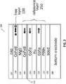
FIG. 2 is a block diagram of an example of a TMR element with a reference layer having a cobalt iron (CoFe) layer and a tantalum layer; -
FIG. 3 is a block diagram of another example of a TMR element with a free layer having the cobalt iron (CoFe) layer and the tantalum layer; -
FIG. 4 is a block diagram of a further example of a TMR element with the reference layer and the free layer each having the cobalt iron (CoFe) layer and the tantalum layer; -
FIG. 5 is a block diagram of a prior art example of a TMR element that is double pinned; and -
FIG. 6 is a block diagram of a still further example of a TMR element that is double pinned with the reference layer and the free layer each having the cobalt iron (CoFe) layer and the tantalum layer. - Described herein are techniques to improve the fabrication of a tunnel junction in a tunneling magnetoresistance (TMR) element by having a reference and/or a free layer include a cobalt iron (CoFe) layer and a tantalum layer. In one example, the techniques described herein teach an alternative approach to incorporating cobalt iron boron (CoFeB)/magnesium oxide (Mg0)/CoFeB layers into a tunnel junction to reduce the impact of a cubic structure with a hexagonal structure.
- Referring to
FIG. 1 , anillustrative TMR element 100 can have astack 102 oflayers layer 106 is a seed layer (e.g., a copper nickel (CuN) layer) with thelayer 110 located on theseed layer 106. Thelayer 110 includes platinum manganese (PtMn) or iridium manganese (IrMn), for example. Thelayer 114 is located on thelayer 110 and thelayer 118 is located on thelayer 114. In one example, thelayer 114 includes cobalt iron (CoFe) and thelayer 118 is a spacer layer and includes ruthenium (Ru). On thelayer 118, a magnesium oxide (MgO)layer 126 is sandwiched between two cobalt iron boron (CoFeB)layers CoFeB layer 128. Thelayer 114 is a single layer pinned layer that is magnetically coupled to thelayer 110. The physical mechanism that iscoupling layers - A
free layer 130 includes theCoFeB layer 128. In some examples, thefree layer 130 may include an additional layer of nickel iron (NiFe) (not shown) and a thin layer of tantalum (not shown) between theCoFeB layer 128 and the NiFe layer. - It will be understood that a driving current running through the
TMR element 100 runs through the layers of the stack, running between seed andcap layers bottom electrode 104. TheTMR element 100 can have a maximum response axis that is parallel to the surface of thebottom electrode 104 and that is in adirection 129, and also parallel to the magnetization direction of thereference layer 150, comprised oflayers - The
TMR element 100 has a maximum response axis (maximum response to external fields) aligned with thearrow 129, i.e., perpendicular to bias directions experienced by thefree layer 130, and parallel to magnetic fields of thereference layer 150, notably pinnedlayer 122. Also, in general, it is rotations of the magnetic direction of thefree layer 130 caused by external magnetic fields that result in changes of resistance of theTMR element 100, which may be due to a change in angle or a change in amplitude if an external bias is present because the sum vector of the external field and the bias is causing a change in the angle between the reference and free layers. - The coherent tunneling mechanism through a magnesium oxide (MgO) barrier (the layer 126) is due to symmetry factors and, as such, it is essential that the MgO barrier and the neighboring
CoFeB layers CoFeB layers - In the
reference layer 150, the main problem of the cubic structure comes from the fact thatCoFeB layer 122 is coupled with anotherCoFe layer 114 through theRu spacer layer 118. The different crystal symmetry makes this coupling less effective than in an all-hexagonal structure. - Referring to
FIG. 2 , to circumvent the difference in crystal symmetry in TMR element 100 (FIG. 1 ), aTMR element 200 replaces the CoFeB layer 122 (FIG. 2 ) with a tri-layer that includes aCoFe layer 222, aTa layer 226 and aCoFeB layer 230. Thelayers reference layer 250 includeslayers - In one example, the
CoFe layer 222 and theCoFeB layer 230 are each about 0.9 nanometers thick. In one example, theTa layer 226 is about 0.1 nanometers thick. In another example, theTa layer 226 ranges from 0.05 nanometers to 0.3 nanometers. - Referring to
FIGS. 1 and3 , in thefree layer 130, the cubic structure of theCoFeB layer 128 causes a higher coercivity in a response. To reduce the coercivity, aTMR element 300 replaces theCoFeB layer 128 with a quad-layer that includes aCoFeB layer 328, aTa layer 336, aCoFe layer 342 and a nickel iron (NiFe) 346 to form a free layer 330. In particular, the thickness ofCoFeB 328 is reduced from theCoFeB layer 128 as much as possible to maintain a good epitaxial structure in the active area. For example, theCoFeB layer 128 is about 2.5 nanometers thick while theCoFeB 328 is about 1.0 nanometers thick. TheCoFe 342 coupled with a magnetically softer material of theNiFe layer 346 helps the rotation of theCoFeB 328 by reducing coercivity. In one example, theCoFe layer 342 is about 1.0 nanometers thick. In one example, theTa layer 336 is about 0.1 nanometers thick. In another example, theTa layer 336 ranges from 0.05 nanometers to 0.3 nanometers. - Referring to
FIG. 4 , both CoFeB layers 122, 128 (FIG. 1 ) may also be replaced. For example, aTMR element 400 includes thereference layer 250 ofFIG. 2 and the free layer 330 ofFIG. 3 . - Referring to
Fig. 5 , aTMR element 500 is the same as TMR element 100 (FIG. 1 ) except, for example, the TMR includes abias layer 590. TheCoFeB 528 forms afree layer 530. Thebias layer 590 includes aRu layer 532 located on theCoFeB layer 528, a CoFe layer located on theRu layer 532 and aPtMn layer 536 located on theCoFe layer 534. - The
TMR element 500 is double pinned, i.e., it has two pinninglayers layer structure layer 536. The single layer pinnedlayer 114 is magnetically coupled to the pinninglayer 110. With zero external magnetic field, thefree layer 530 takes on a magnetic alignment parallel to thebias layer 590, with direction (ferromagnetic or antiferromagnetic coupling) determined by thickness and material of thespacer layer 532. Thus, double pinned means that thefree layer 530 is stabilized by intra-stack bias from thebias layer 590. Thefree layer 530 may go parallel or antiparallel to thereference layer 150 depending on the direction of theexternal field 129. - Referring to
FIG. 6 , the techniques described inFIGS. 2 to 4 may also be applied to the TMR element 500 (FIG. 5 ). For example, in aTMR element 600, the free layer 530 (FIG. 5 ) is replaced with the free layer 330 and the reference layer 150 (FIG. 5 ) is replaced with thereference layer 250. - Elements of different embodiments described herein may be combined to form other embodiments not specifically set forth above. Various elements, which are described in the context of a single embodiment, may also be provided separately or in any suitable subcombination. Other embodiments not specifically described herein are also within the scope of the following claims.
Claims (18)
- A tunnel magnetoresistance (TMR) element, comprising:a magnesium oxide (MgO) layer;a cobalt iron boron (CoFeB) layer in direct contact with the MgO layer;a cobalt iron (CoFe) layer; anda tantalum layer in direct contact with the CoFeB layer and the CoFe layer.
- The TMR of claim 1, wherein the CoFeB layer, the CoFe layer and the tantalum layer are part of a reference layer.
- The TMR of claim 2, wherein the CoFeB layer is about 0.9 nanometers thick.
- The TMR of claim 2, wherein the CoFe layer is about 0.9 nanometers thick.
- The TMR of claim 1, wherein the tantalum layer is about 0.1 nanometers thick.
- The TMR of claim 1, wherein a thickness of the tantalum layer is between 0.05 nanometers and 0.3 nanometers.
- The TMR of claim 1, wherein the CoFeB layer, the CoFe layer and the tantalum layer are part of a free layer.
- The TMR of claim 7, wherein the free layer comprises a nickel iron (NiFe) layer, the NiFe layer is in direct contact with the CoFe layer.
- The TMR of claim 7, wherein the CoFeB layer is about 1.0 nanometer thick.
- The TMR of claim 7, wherein the CoFe layer is about 1.0 nanometer thick.
- The TMR of claim 1, wherein the CoFeB layer is a first CoFeB layer, the CoFe layer is a first CoFe layer and the tantalum layer is a first tantalum layer;
wherein the first CoFeB layer, the first CoFe layer and the first tantalum layer are part of a reference layer, and
further comprising:a second CoFeB layer in direct contact with the MgO layer;a second CoFe layer; anda second tantalum layer in direct contact with the second CoFeB layer and the second CoFe layer,wherein the second CoFeB layer, the second CoFe layer and the second tantalum layer are part of a free layer. - The TMR of claim 11, wherein the first CoFeB layer is about 0.9 nanometers thick,
wherein the first CoFe layer is about 0.9 nanometers thick,
wherein the second CoFeB layer is about 1.0 nanometer thick, and
wherein the second CoFe layer is about 1.0 nanometer thick. - The TMR of claim 12, wherein the second tantalum layer is about 0.1 nanometers thick.
- The TMR of claim 12, wherein a thickness of the second tantalum layer is between 0.05 nanometers and 0.3 nanometers.
- The TMR of claim 11, further comprising a bias layer in direct contact with the free layer.
- The TMR of claim 15, wherein the bias layer comprises a third CoFe layer.
- The TMR of claim 1, wherein the TMR is single pinned.
- The TMR of claim 1, wherein the TMR is double pinned.
Applications Claiming Priority (2)
| Application Number | Priority Date | Filing Date | Title |
|---|---|---|---|
| US201962894114P | 2019-08-30 | 2019-08-30 | |
| US16/574,419 US11127518B2 (en) | 2019-08-30 | 2019-09-18 | Tunnel magnetoresistance (TMR) element having cobalt iron and tantalum layers |
Publications (2)
| Publication Number | Publication Date |
|---|---|
| EP3786957A1 true EP3786957A1 (en) | 2021-03-03 |
| EP3786957B1 EP3786957B1 (en) | 2023-06-21 |
Family
ID=72243055
Family Applications (1)
| Application Number | Title | Priority Date | Filing Date |
|---|---|---|---|
| EP20192931.2A Active EP3786957B1 (en) | 2019-08-30 | 2020-08-26 | Tunnel magnetoresistance (tmr) element having cobalt iron and tantalum layers |
Country Status (2)
| Country | Link |
|---|---|
| US (2) | US11127518B2 (en) |
| EP (1) | EP3786957B1 (en) |
Families Citing this family (7)
| Publication number | Priority date | Publication date | Assignee | Title |
|---|---|---|---|---|
| EP3879543B1 (en) * | 2020-03-11 | 2024-11-27 | Allegro MicroSystems, LLC | Method for manufacturing a magnetoresistive sensor element for sensing a two-dimensional magnetic field with low high-field error |
| US11630168B2 (en) | 2021-02-03 | 2023-04-18 | Allegro Microsystems, Llc | Linear sensor with dual spin valve element having reference layers with magnetization directions different from an external magnetic field direction |
| US11719771B1 (en) | 2022-06-02 | 2023-08-08 | Allegro Microsystems, Llc | Magnetoresistive sensor having seed layer hysteresis suppression |
| US12320870B2 (en) | 2022-07-19 | 2025-06-03 | Allegro Microsystems, Llc | Controlling out-of-plane anisotropy in an MR sensor with free layer dusting |
| US12000870B2 (en) | 2022-09-12 | 2024-06-04 | Allegro Microsystems, Llc | Multi-terminal devices using magnetoresistance elements |
| US12181538B2 (en) | 2022-11-29 | 2024-12-31 | Allegro Microsystems, Llc | Magnetoresistance bridge circuits with stray field immunity |
| US12510609B2 (en) | 2024-02-13 | 2025-12-30 | Allegro Microsystems, Llc | Magnetoresistance element including a multi-layered free layer stack to tune hysteresis and output amplitude |
Citations (8)
| Publication number | Priority date | Publication date | Assignee | Title |
|---|---|---|---|---|
| US6937497B1 (en) * | 2004-11-18 | 2005-08-30 | Maglabs, Inc. | Magnetic random access memory with stacked toggle memory cells |
| US20070253118A1 (en) * | 2006-04-26 | 2007-11-01 | Jun Hayakawa | Tunnel magnetic resistance device, and magnetic memory cell and magnetic random access memory using the same |
| US20120070695A1 (en) * | 2010-09-16 | 2012-03-22 | Kabushiki Kaisha Toshiba | Magnetoresistive element |
| US20120280336A1 (en) * | 2011-05-04 | 2012-11-08 | Magic Technologies, Inc. | Multilayers having reduced perpendicular demagnetizing field using moment dilution for spintronic applications |
| EP2880665A1 (en) * | 2012-07-30 | 2015-06-10 | Magic Technologies Inc. | Co/ni multilayers with improved out-of plane anisotropy for magnetic device applications |
| US20160204341A1 (en) * | 2011-02-16 | 2016-07-14 | Avalanche Technology, Inc. | Magnetic random access memory with perpendicular enhancement layer |
| EP3288091A1 (en) * | 2016-08-26 | 2018-02-28 | Allegro Microsystems, LLC | Double pinned magnetoresistance element with temporary ferromagnetic layer to improve annealing |
| US20190051822A1 (en) * | 2017-08-10 | 2019-02-14 | Commissariat A L'energie Atomique Et Aux Energies Alternatives | Synthetic antiferromagnetic layer, magnetic tunnel junction and spintronic device using said synthetic antiferromagnetic layer |
Family Cites Families (25)
| Publication number | Priority date | Publication date | Assignee | Title |
|---|---|---|---|---|
| US6473275B1 (en) | 2000-06-06 | 2002-10-29 | International Business Machines Corporation | Dual hybrid magnetic tunnel junction/giant magnetoresistive sensor |
| JP2002150511A (en) | 2000-11-06 | 2002-05-24 | Fujitsu Ltd | Spin valve magnetoresistive element and magnetic head using the same |
| US6709767B2 (en) | 2001-07-31 | 2004-03-23 | Hitachi Global Storage Technologies Netherlands B.V. | In-situ oxidized films for use as cap and gap layers in a spin-valve sensor and methods of manufacture |
| US7161771B2 (en) | 2002-04-02 | 2007-01-09 | Hitachi Global Storage Technologies Netherlands B.V. | Dual spin valve sensor with a longitudinal bias stack |
| US6985385B2 (en) | 2003-08-26 | 2006-01-10 | Grandis, Inc. | Magnetic memory element utilizing spin transfer switching and storing multiple bits |
| US7639459B2 (en) | 2005-01-10 | 2009-12-29 | Hitachi Global Storage Technologies Netherlands B.V. | Three terminal magnetic sensor having an in-stack longitudinal biasing layer structure |
| US7453720B2 (en) | 2005-05-26 | 2008-11-18 | Maglabs, Inc. | Magnetic random access memory with stacked toggle memory cells having oppositely-directed easy-axis biasing |
| US7973349B2 (en) | 2005-09-20 | 2011-07-05 | Grandis Inc. | Magnetic device having multilayered free ferromagnetic layer |
| DE102006010652B4 (en) | 2006-03-06 | 2008-02-14 | Bundesrepublik Deutschland, vertr. durch d. Bundesministerium f. Wirtschaft und Technologie, dieses vertreten durch d. Präsidenten d. Physikalisch-Technischen Bundesanstalt | magnetic field sensor |
| JP4780117B2 (en) | 2008-01-30 | 2011-09-28 | 日立金属株式会社 | Angle sensor, manufacturing method thereof, and angle detection device using the same |
| US9007055B2 (en) | 2008-09-12 | 2015-04-14 | Hitachi Metals, Ltd. | Self-pinned spin valve magnetoresistance effect film and magnetic sensor using the same, and rotation angle detection device |
| JP2010080008A (en) | 2008-09-26 | 2010-04-08 | Fujitsu Ltd | Reproduction magnetic head |
| WO2011007767A1 (en) | 2009-07-13 | 2011-01-20 | 日立金属株式会社 | Method for producing magnetoresistive effect element, magnetic sensor, rotation-angle detection device |
| US8445979B2 (en) | 2009-09-11 | 2013-05-21 | Samsung Electronics Co., Ltd. | Magnetic memory devices including magnetic layers separated by tunnel barriers |
| US20110169488A1 (en) | 2010-01-08 | 2011-07-14 | Everspin Technologies, Inc. | Method and structure for testing and calibrating magnetic field sensing device |
| US8780665B2 (en) | 2010-08-11 | 2014-07-15 | Samsung Electronics Co., Ltd. | Method and system for providing magnetic tunneling junction elements having an easy cone anisotropy |
| KR102199622B1 (en) | 2013-01-11 | 2021-01-08 | 삼성전자주식회사 | Method and system for providing magnetic tunneling juntion elements having easy cone anisotropy |
| US9529060B2 (en) | 2014-01-09 | 2016-12-27 | Allegro Microsystems, Llc | Magnetoresistance element with improved response to magnetic fields |
| US9958511B2 (en) | 2014-12-08 | 2018-05-01 | Infineon Technologies Ag | Soft switching of magnetization in a magnetoresistive sensor |
| EP3300534B1 (en) | 2015-06-05 | 2020-11-11 | Allegro MicroSystems, LLC | Spin valve magnetoresistance element with improved response to magnetic fields |
| US10060880B2 (en) | 2016-09-15 | 2018-08-28 | Qualcomm Incorporated | Magnetoresistive (MR) sensors employing dual MR devices for differential MR sensing |
| US11022661B2 (en) | 2017-05-19 | 2021-06-01 | Allegro Microsystems, Llc | Magnetoresistance element with increased operational range |
| US10620279B2 (en) | 2017-05-19 | 2020-04-14 | Allegro Microsystems, Llc | Magnetoresistance element with increased operational range |
| US10509058B2 (en) | 2018-01-12 | 2019-12-17 | Allegro Microsystems, Llc | Current sensor using modulation of or change of sensitivity of magnetoresistance elements |
| US10578684B2 (en) | 2018-01-12 | 2020-03-03 | Allegro Microsystems, Llc | Magnetic field sensor having magnetoresistance elements with opposite bias directions |
-
2019
- 2019-09-18 US US16/574,419 patent/US11127518B2/en active Active
-
2020
- 2020-08-26 EP EP20192931.2A patent/EP3786957B1/en active Active
-
2021
- 2021-08-18 US US17/405,490 patent/US20210383953A1/en not_active Abandoned
Patent Citations (8)
| Publication number | Priority date | Publication date | Assignee | Title |
|---|---|---|---|---|
| US6937497B1 (en) * | 2004-11-18 | 2005-08-30 | Maglabs, Inc. | Magnetic random access memory with stacked toggle memory cells |
| US20070253118A1 (en) * | 2006-04-26 | 2007-11-01 | Jun Hayakawa | Tunnel magnetic resistance device, and magnetic memory cell and magnetic random access memory using the same |
| US20120070695A1 (en) * | 2010-09-16 | 2012-03-22 | Kabushiki Kaisha Toshiba | Magnetoresistive element |
| US20160204341A1 (en) * | 2011-02-16 | 2016-07-14 | Avalanche Technology, Inc. | Magnetic random access memory with perpendicular enhancement layer |
| US20120280336A1 (en) * | 2011-05-04 | 2012-11-08 | Magic Technologies, Inc. | Multilayers having reduced perpendicular demagnetizing field using moment dilution for spintronic applications |
| EP2880665A1 (en) * | 2012-07-30 | 2015-06-10 | Magic Technologies Inc. | Co/ni multilayers with improved out-of plane anisotropy for magnetic device applications |
| EP3288091A1 (en) * | 2016-08-26 | 2018-02-28 | Allegro Microsystems, LLC | Double pinned magnetoresistance element with temporary ferromagnetic layer to improve annealing |
| US20190051822A1 (en) * | 2017-08-10 | 2019-02-14 | Commissariat A L'energie Atomique Et Aux Energies Alternatives | Synthetic antiferromagnetic layer, magnetic tunnel junction and spintronic device using said synthetic antiferromagnetic layer |
Non-Patent Citations (2)
| Title |
|---|
| YUAN Z H ET AL: "Double-pinned magnetic tunnel junction sensors with spin-valve-like sensing layers", JOURNAL OF APPLIED PHYSICS, AMERICAN INSTITUTE OF PHYSICS, US, vol. 118, no. 5, 7 August 2015 (2015-08-07), XP012199505, ISSN: 0021-8979, [retrieved on 19010101], DOI: 10.1063/1.4927840 * |
| ZHANG XU ET AL: "Large Perpendicular Exchange Bias in CoFeB/MgO Systems Pinned by a Bottom IrMn Layer via an Interfacial CoFe/Ta Composite Layer", IEEE TRANSACTIONS ON MAGNETICS, IEEE SERVICE CENTER, NEW YORK, NY, US, vol. 51, no. 11, 11 November 2015 (2015-11-11), pages 1 - 4, XP011587639, ISSN: 0018-9464, [retrieved on 20151023], DOI: 10.1109/TMAG.2015.2443079 * |
Also Published As
| Publication number | Publication date |
|---|---|
| US20210383953A1 (en) | 2021-12-09 |
| US20210065949A1 (en) | 2021-03-04 |
| EP3786957B1 (en) | 2023-06-21 |
| US11127518B2 (en) | 2021-09-21 |
Similar Documents
| Publication | Publication Date | Title |
|---|---|---|
| EP3786957B1 (en) | Tunnel magnetoresistance (tmr) element having cobalt iron and tantalum layers | |
| US10718830B2 (en) | Magnetoresistive sensor | |
| EP3092505B1 (en) | Magnetoresistance element with an improved seed layer to promote an improved response to magnetic fields | |
| US9207290B2 (en) | Magnetic field sensor for sensing external magnetic field | |
| US8816456B2 (en) | Magnetoresistive device and a method of forming the same | |
| US7280323B2 (en) | Magnetoresistance effect element and magnetic head | |
| US7476954B2 (en) | TMR device with Hf based seed layer | |
| US20080239589A1 (en) | Spin transfer MRAM device with novel magnetic synthetic free layer | |
| US11217626B2 (en) | Dual tunnel magnetoresistance (TMR) element structure | |
| US20020154455A1 (en) | Magnetic device with a coupling layer and method of manufacturing and operation of such device | |
| US11385306B2 (en) | TMR sensor with magnetic tunnel junctions with shape anisotropy | |
| US11199594B2 (en) | TMR sensor with magnetic tunnel junctions with a free layer having an intrinsic anisotropy | |
| US9810747B2 (en) | Magnetic sensor and magnetic encoder | |
| US20080247097A1 (en) | Magnetoresistance effect element and magnetic head | |
| US20050068698A1 (en) | Magnetoresistance effect element and magnetic head | |
| US10663537B2 (en) | Magnetic sensor cell for measuring one- and two-dimensional magnetic fields and method for measuring said magnetic fields using the magnetic sensor cell | |
| JP6586974B2 (en) | Magnetoresistive effect element | |
| WO2015129235A1 (en) | Magnetic sensor | |
| US10665774B2 (en) | Magnetoresistive element having an adjustable magnetostriction and magnetic device comprising this magnetoresistive element | |
| US20240094314A1 (en) | Multiple cobalt iron boron layers in a free layer of a magnetoresistive sensing element | |
| US20250383414A1 (en) | Tunnel magnetoresistance element and sensor having increased measurement range | |
| US20250264551A1 (en) | Method for manufacturing magnetic sensor and magnetic sensor | |
| WO2018185608A1 (en) | Magnetic sensor cell for measuring one- and two-dimensional magnetic fields and method for measuring said magnetic fields using the magnetic sensor cell | |
| EP3975184A1 (en) | Magnetic random access memory cell comprising a ferrimagnetic free layer | |
| EP3385741B1 (en) | Magnetic sensor cell for measuring one- and two-dimensional magnetic fields and method for measuring said magnetic fields using the magnetic sensor cell |
Legal Events
| Date | Code | Title | Description |
|---|---|---|---|
| PUAI | Public reference made under article 153(3) epc to a published international application that has entered the european phase |
Free format text: ORIGINAL CODE: 0009012 |
|
| STAA | Information on the status of an ep patent application or granted ep patent |
Free format text: STATUS: THE APPLICATION HAS BEEN PUBLISHED |
|
| AK | Designated contracting states |
Kind code of ref document: A1 Designated state(s): AL AT BE BG CH CY CZ DE DK EE ES FI FR GB GR HR HU IE IS IT LI LT LU LV MC MK MT NL NO PL PT RO RS SE SI SK SM TR |
|
| AX | Request for extension of the european patent |
Extension state: BA ME |
|
| STAA | Information on the status of an ep patent application or granted ep patent |
Free format text: STATUS: REQUEST FOR EXAMINATION WAS MADE |
|
| 17P | Request for examination filed |
Effective date: 20210902 |
|
| RBV | Designated contracting states (corrected) |
Designated state(s): AL AT BE BG CH CY CZ DE DK EE ES FI FR GB GR HR HU IE IS IT LI LT LU LV MC MK MT NL NO PL PT RO RS SE SI SK SM TR |
|
| RIC1 | Information provided on ipc code assigned before grant |
Ipc: H10N 50/85 20230101ALI20230123BHEP Ipc: H10N 50/10 20230101ALI20230123BHEP Ipc: G11C 11/16 20060101AFI20230123BHEP |
|
| GRAP | Despatch of communication of intention to grant a patent |
Free format text: ORIGINAL CODE: EPIDOSNIGR1 |
|
| STAA | Information on the status of an ep patent application or granted ep patent |
Free format text: STATUS: GRANT OF PATENT IS INTENDED |
|
| INTG | Intention to grant announced |
Effective date: 20230316 |
|
| GRAS | Grant fee paid |
Free format text: ORIGINAL CODE: EPIDOSNIGR3 |
|
| GRAA | (expected) grant |
Free format text: ORIGINAL CODE: 0009210 |
|
| STAA | Information on the status of an ep patent application or granted ep patent |
Free format text: STATUS: THE PATENT HAS BEEN GRANTED |
|
| AK | Designated contracting states |
Kind code of ref document: B1 Designated state(s): AL AT BE BG CH CY CZ DE DK EE ES FI FR GB GR HR HU IE IS IT LI LT LU LV MC MK MT NL NO PL PT RO RS SE SI SK SM TR |
|
| REG | Reference to a national code |
Ref country code: CH Ref legal event code: EP |
|
| REG | Reference to a national code |
Ref country code: DE Ref legal event code: R096 Ref document number: 602020012700 Country of ref document: DE |
|
| REG | Reference to a national code |
Ref country code: AT Ref legal event code: REF Ref document number: 1581492 Country of ref document: AT Kind code of ref document: T Effective date: 20230715 |
|
| REG | Reference to a national code |
Ref country code: IE Ref legal event code: FG4D |
|
| REG | Reference to a national code |
Ref country code: LT Ref legal event code: MG9D |
|
| REG | Reference to a national code |
Ref country code: NL Ref legal event code: MP Effective date: 20230621 |
|
| PG25 | Lapsed in a contracting state [announced via postgrant information from national office to epo] |
Ref country code: SE Free format text: LAPSE BECAUSE OF FAILURE TO SUBMIT A TRANSLATION OF THE DESCRIPTION OR TO PAY THE FEE WITHIN THE PRESCRIBED TIME-LIMIT Effective date: 20230621 Ref country code: NO Free format text: LAPSE BECAUSE OF FAILURE TO SUBMIT A TRANSLATION OF THE DESCRIPTION OR TO PAY THE FEE WITHIN THE PRESCRIBED TIME-LIMIT Effective date: 20230921 |
|
| REG | Reference to a national code |
Ref country code: AT Ref legal event code: MK05 Ref document number: 1581492 Country of ref document: AT Kind code of ref document: T Effective date: 20230621 |
|
| PG25 | Lapsed in a contracting state [announced via postgrant information from national office to epo] |
Ref country code: RS Free format text: LAPSE BECAUSE OF FAILURE TO SUBMIT A TRANSLATION OF THE DESCRIPTION OR TO PAY THE FEE WITHIN THE PRESCRIBED TIME-LIMIT Effective date: 20230621 Ref country code: NL Free format text: LAPSE BECAUSE OF FAILURE TO SUBMIT A TRANSLATION OF THE DESCRIPTION OR TO PAY THE FEE WITHIN THE PRESCRIBED TIME-LIMIT Effective date: 20230621 Ref country code: LV Free format text: LAPSE BECAUSE OF FAILURE TO SUBMIT A TRANSLATION OF THE DESCRIPTION OR TO PAY THE FEE WITHIN THE PRESCRIBED TIME-LIMIT Effective date: 20230621 Ref country code: LT Free format text: LAPSE BECAUSE OF FAILURE TO SUBMIT A TRANSLATION OF THE DESCRIPTION OR TO PAY THE FEE WITHIN THE PRESCRIBED TIME-LIMIT Effective date: 20230621 Ref country code: HR Free format text: LAPSE BECAUSE OF FAILURE TO SUBMIT A TRANSLATION OF THE DESCRIPTION OR TO PAY THE FEE WITHIN THE PRESCRIBED TIME-LIMIT Effective date: 20230621 Ref country code: GR Free format text: LAPSE BECAUSE OF FAILURE TO SUBMIT A TRANSLATION OF THE DESCRIPTION OR TO PAY THE FEE WITHIN THE PRESCRIBED TIME-LIMIT Effective date: 20230922 |
|
| PG25 | Lapsed in a contracting state [announced via postgrant information from national office to epo] |
Ref country code: FI Free format text: LAPSE BECAUSE OF FAILURE TO SUBMIT A TRANSLATION OF THE DESCRIPTION OR TO PAY THE FEE WITHIN THE PRESCRIBED TIME-LIMIT Effective date: 20230621 |
|
| PG25 | Lapsed in a contracting state [announced via postgrant information from national office to epo] |
Ref country code: SK Free format text: LAPSE BECAUSE OF FAILURE TO SUBMIT A TRANSLATION OF THE DESCRIPTION OR TO PAY THE FEE WITHIN THE PRESCRIBED TIME-LIMIT Effective date: 20230621 |
|
| PG25 | Lapsed in a contracting state [announced via postgrant information from national office to epo] |
Ref country code: ES Free format text: LAPSE BECAUSE OF FAILURE TO SUBMIT A TRANSLATION OF THE DESCRIPTION OR TO PAY THE FEE WITHIN THE PRESCRIBED TIME-LIMIT Effective date: 20230621 |
|
| PG25 | Lapsed in a contracting state [announced via postgrant information from national office to epo] |
Ref country code: IS Free format text: LAPSE BECAUSE OF FAILURE TO SUBMIT A TRANSLATION OF THE DESCRIPTION OR TO PAY THE FEE WITHIN THE PRESCRIBED TIME-LIMIT Effective date: 20231021 |
|
| PG25 | Lapsed in a contracting state [announced via postgrant information from national office to epo] |
Ref country code: SM Free format text: LAPSE BECAUSE OF FAILURE TO SUBMIT A TRANSLATION OF THE DESCRIPTION OR TO PAY THE FEE WITHIN THE PRESCRIBED TIME-LIMIT Effective date: 20230621 Ref country code: SK Free format text: LAPSE BECAUSE OF FAILURE TO SUBMIT A TRANSLATION OF THE DESCRIPTION OR TO PAY THE FEE WITHIN THE PRESCRIBED TIME-LIMIT Effective date: 20230621 Ref country code: RO Free format text: LAPSE BECAUSE OF FAILURE TO SUBMIT A TRANSLATION OF THE DESCRIPTION OR TO PAY THE FEE WITHIN THE PRESCRIBED TIME-LIMIT Effective date: 20230621 Ref country code: PT Free format text: LAPSE BECAUSE OF FAILURE TO SUBMIT A TRANSLATION OF THE DESCRIPTION OR TO PAY THE FEE WITHIN THE PRESCRIBED TIME-LIMIT Effective date: 20231023 Ref country code: IS Free format text: LAPSE BECAUSE OF FAILURE TO SUBMIT A TRANSLATION OF THE DESCRIPTION OR TO PAY THE FEE WITHIN THE PRESCRIBED TIME-LIMIT Effective date: 20231021 Ref country code: ES Free format text: LAPSE BECAUSE OF FAILURE TO SUBMIT A TRANSLATION OF THE DESCRIPTION OR TO PAY THE FEE WITHIN THE PRESCRIBED TIME-LIMIT Effective date: 20230621 Ref country code: EE Free format text: LAPSE BECAUSE OF FAILURE TO SUBMIT A TRANSLATION OF THE DESCRIPTION OR TO PAY THE FEE WITHIN THE PRESCRIBED TIME-LIMIT Effective date: 20230621 Ref country code: CZ Free format text: LAPSE BECAUSE OF FAILURE TO SUBMIT A TRANSLATION OF THE DESCRIPTION OR TO PAY THE FEE WITHIN THE PRESCRIBED TIME-LIMIT Effective date: 20230621 Ref country code: AT Free format text: LAPSE BECAUSE OF FAILURE TO SUBMIT A TRANSLATION OF THE DESCRIPTION OR TO PAY THE FEE WITHIN THE PRESCRIBED TIME-LIMIT Effective date: 20230621 |
|
| PG25 | Lapsed in a contracting state [announced via postgrant information from national office to epo] |
Ref country code: PL Free format text: LAPSE BECAUSE OF FAILURE TO SUBMIT A TRANSLATION OF THE DESCRIPTION OR TO PAY THE FEE WITHIN THE PRESCRIBED TIME-LIMIT Effective date: 20230621 |
|
| PG25 | Lapsed in a contracting state [announced via postgrant information from national office to epo] |
Ref country code: MC Free format text: LAPSE BECAUSE OF FAILURE TO SUBMIT A TRANSLATION OF THE DESCRIPTION OR TO PAY THE FEE WITHIN THE PRESCRIBED TIME-LIMIT Effective date: 20230621 |
|
| REG | Reference to a national code |
Ref country code: DE Ref legal event code: R097 Ref document number: 602020012700 Country of ref document: DE |
|
| REG | Reference to a national code |
Ref country code: CH Ref legal event code: PL |
|
| PG25 | Lapsed in a contracting state [announced via postgrant information from national office to epo] |
Ref country code: MC Free format text: LAPSE BECAUSE OF FAILURE TO SUBMIT A TRANSLATION OF THE DESCRIPTION OR TO PAY THE FEE WITHIN THE PRESCRIBED TIME-LIMIT Effective date: 20230621 |
|
| PG25 | Lapsed in a contracting state [announced via postgrant information from national office to epo] |
Ref country code: LU Free format text: LAPSE BECAUSE OF NON-PAYMENT OF DUE FEES Effective date: 20230826 |
|
| PLBE | No opposition filed within time limit |
Free format text: ORIGINAL CODE: 0009261 |
|
| STAA | Information on the status of an ep patent application or granted ep patent |
Free format text: STATUS: NO OPPOSITION FILED WITHIN TIME LIMIT |
|
| PG25 | Lapsed in a contracting state [announced via postgrant information from national office to epo] |
Ref country code: LU Free format text: LAPSE BECAUSE OF NON-PAYMENT OF DUE FEES Effective date: 20230826 Ref country code: DK Free format text: LAPSE BECAUSE OF FAILURE TO SUBMIT A TRANSLATION OF THE DESCRIPTION OR TO PAY THE FEE WITHIN THE PRESCRIBED TIME-LIMIT Effective date: 20230621 Ref country code: CH Free format text: LAPSE BECAUSE OF NON-PAYMENT OF DUE FEES Effective date: 20230831 |
|
| PG25 | Lapsed in a contracting state [announced via postgrant information from national office to epo] |
Ref country code: SI Free format text: LAPSE BECAUSE OF FAILURE TO SUBMIT A TRANSLATION OF THE DESCRIPTION OR TO PAY THE FEE WITHIN THE PRESCRIBED TIME-LIMIT Effective date: 20230621 |
|
| REG | Reference to a national code |
Ref country code: BE Ref legal event code: MM Effective date: 20230831 |
|
| REG | Reference to a national code |
Ref country code: IE Ref legal event code: MM4A |
|
| 26N | No opposition filed |
Effective date: 20240322 |
|
| PG25 | Lapsed in a contracting state [announced via postgrant information from national office to epo] |
Ref country code: SI Free format text: LAPSE BECAUSE OF FAILURE TO SUBMIT A TRANSLATION OF THE DESCRIPTION OR TO PAY THE FEE WITHIN THE PRESCRIBED TIME-LIMIT Effective date: 20230621 Ref country code: IT Free format text: LAPSE BECAUSE OF FAILURE TO SUBMIT A TRANSLATION OF THE DESCRIPTION OR TO PAY THE FEE WITHIN THE PRESCRIBED TIME-LIMIT Effective date: 20230621 |
|
| PG25 | Lapsed in a contracting state [announced via postgrant information from national office to epo] |
Ref country code: IE Free format text: LAPSE BECAUSE OF NON-PAYMENT OF DUE FEES Effective date: 20230826 |
|
| PG25 | Lapsed in a contracting state [announced via postgrant information from national office to epo] |
Ref country code: IE Free format text: LAPSE BECAUSE OF NON-PAYMENT OF DUE FEES Effective date: 20230826 |
|
| PG25 | Lapsed in a contracting state [announced via postgrant information from national office to epo] |
Ref country code: BE Free format text: LAPSE BECAUSE OF NON-PAYMENT OF DUE FEES Effective date: 20230831 |
|
| PG25 | Lapsed in a contracting state [announced via postgrant information from national office to epo] |
Ref country code: BG Free format text: LAPSE BECAUSE OF FAILURE TO SUBMIT A TRANSLATION OF THE DESCRIPTION OR TO PAY THE FEE WITHIN THE PRESCRIBED TIME-LIMIT Effective date: 20230621 |
|
| PG25 | Lapsed in a contracting state [announced via postgrant information from national office to epo] |
Ref country code: BG Free format text: LAPSE BECAUSE OF FAILURE TO SUBMIT A TRANSLATION OF THE DESCRIPTION OR TO PAY THE FEE WITHIN THE PRESCRIBED TIME-LIMIT Effective date: 20230621 |
|
| GBPC | Gb: european patent ceased through non-payment of renewal fee |
Effective date: 20240826 |
|
| PG25 | Lapsed in a contracting state [announced via postgrant information from national office to epo] |
Ref country code: GB Free format text: LAPSE BECAUSE OF NON-PAYMENT OF DUE FEES Effective date: 20240826 |
|
| PG25 | Lapsed in a contracting state [announced via postgrant information from national office to epo] |
Ref country code: CY Free format text: LAPSE BECAUSE OF FAILURE TO SUBMIT A TRANSLATION OF THE DESCRIPTION OR TO PAY THE FEE WITHIN THE PRESCRIBED TIME-LIMIT; INVALID AB INITIO Effective date: 20200826 |
|
| PG25 | Lapsed in a contracting state [announced via postgrant information from national office to epo] |
Ref country code: HU Free format text: LAPSE BECAUSE OF FAILURE TO SUBMIT A TRANSLATION OF THE DESCRIPTION OR TO PAY THE FEE WITHIN THE PRESCRIBED TIME-LIMIT; INVALID AB INITIO Effective date: 20200826 |
|
| PGFP | Annual fee paid to national office [announced via postgrant information from national office to epo] |
Ref country code: DE Payment date: 20250702 Year of fee payment: 6 |
|
| PGFP | Annual fee paid to national office [announced via postgrant information from national office to epo] |
Ref country code: FR Payment date: 20250703 Year of fee payment: 6 |
|
| PG25 | Lapsed in a contracting state [announced via postgrant information from national office to epo] |
Ref country code: TR Free format text: LAPSE BECAUSE OF FAILURE TO SUBMIT A TRANSLATION OF THE DESCRIPTION OR TO PAY THE FEE WITHIN THE PRESCRIBED TIME-LIMIT Effective date: 20230621 |