EP3786858A1 - Method and system for coupling any two bits from among multiple superconductor quantum bits - Google Patents
Method and system for coupling any two bits from among multiple superconductor quantum bits Download PDFInfo
- Publication number
- EP3786858A1 EP3786858A1 EP19792154.7A EP19792154A EP3786858A1 EP 3786858 A1 EP3786858 A1 EP 3786858A1 EP 19792154 A EP19792154 A EP 19792154A EP 3786858 A1 EP3786858 A1 EP 3786858A1
- Authority
- EP
- European Patent Office
- Prior art keywords
- qubit
- spin
- coupling
- superconducting
- qubits
- Prior art date
- Legal status (The legal status is an assumption and is not a legal conclusion. Google has not performed a legal analysis and makes no representation as to the accuracy of the status listed.)
- Granted
Links
Images


Classifications
-
- B—PERFORMING OPERATIONS; TRANSPORTING
- B82—NANOTECHNOLOGY
- B82Y—SPECIFIC USES OR APPLICATIONS OF NANOSTRUCTURES; MEASUREMENT OR ANALYSIS OF NANOSTRUCTURES; MANUFACTURE OR TREATMENT OF NANOSTRUCTURES
- B82Y25/00—Nanomagnetism, e.g. magnetoimpedance, anisotropic magnetoresistance, giant magnetoresistance or tunneling magnetoresistance
-
- G—PHYSICS
- G06—COMPUTING OR CALCULATING; COUNTING
- G06N—COMPUTING ARRANGEMENTS BASED ON SPECIFIC COMPUTATIONAL MODELS
- G06N10/00—Quantum computing, i.e. information processing based on quantum-mechanical phenomena
- G06N10/40—Physical realisations or architectures of quantum processors or components for manipulating qubits, e.g. qubit coupling or qubit control
-
- H—ELECTRICITY
- H10—SEMICONDUCTOR DEVICES; ELECTRIC SOLID-STATE DEVICES NOT OTHERWISE PROVIDED FOR
- H10N—ELECTRIC SOLID-STATE DEVICES NOT OTHERWISE PROVIDED FOR
- H10N50/00—Galvanomagnetic devices
- H10N50/20—Spin-polarised current-controlled devices
-
- H—ELECTRICITY
- H10—SEMICONDUCTOR DEVICES; ELECTRIC SOLID-STATE DEVICES NOT OTHERWISE PROVIDED FOR
- H10N—ELECTRIC SOLID-STATE DEVICES NOT OTHERWISE PROVIDED FOR
- H10N69/00—Integrated devices, or assemblies of multiple devices, comprising at least one superconducting element covered by group H10N60/00
-
- B—PERFORMING OPERATIONS; TRANSPORTING
- B82—NANOTECHNOLOGY
- B82Y—SPECIFIC USES OR APPLICATIONS OF NANOSTRUCTURES; MEASUREMENT OR ANALYSIS OF NANOSTRUCTURES; MANUFACTURE OR TREATMENT OF NANOSTRUCTURES
- B82Y10/00—Nanotechnology for information processing, storage or transmission, e.g. quantum computing or single electron logic
Definitions
- the present application relates to the field of superconducting quantum technology, and, in particular, to a method for coupling any two qubits from among multiple superconducting qubits.
- Superconducting qubits are considered as one of the most promising solid-state method for implementing a quantum computer due to their advantages in controllability, low loss and scalability. Coherent controllable coupling between qubits is a necessary condition for achieving large-scale quantum computation.
- a method for coupling any two qubits from among multiple superconducting qubits is provided in the present disclosure.
- the method is applied to an occasion provided with a multi-superconducting qubit array and a magnetic film material 100 capable of implementing spin waves.
- the method includes the steps described below.
- the magnetic film material 100 is disposed below the multi-superconducting-qubit array 200.
- Multiple spin wave channels through which the spin waves pass are formed through a combination of magnetization directions of magnetic domains in the magnetic film material 100.
- Multiple qubits of the multi-superconducting-qubit array are disposed above the multiple spin wave channels through which the spin waves pass correspondingly, so as to implement a coupling between each qubit and the spin waves.
- At least two qubits are disposed above one spin wave channel through which the spin waves pass.
- the coupling between the at least two qubits is implemented through the coupling between the each of the at least two qubits and the spin waves.
- a structure where a superconducting qubit layer and a magnetic film material 100 layer are disposed in an upper layer and a lower layer along the vertical direction respectively is adopted, and the state change of the each qubit of the superconducting qubit layer is transferred through the spin waves of the magnetic film material 100 layer.
- the coupling between any two superconducting qubits is implemented through both the soft connection of the spin waves, and the coupling between the each superconducting qubit and the spin waves.
- the multiple spin wave channels through which the spin waves pass are changed by changing the combination of the magnetization directions of the magnetic domains in the magnetic film material.
- the spin waves at least include a first spin and a second spin.
- the first spin correspondingly acts on a first qubit of the multi-superconducting-qubit array.
- the second spin correspondingly acts on a second qubit of the multi-superconducting-qubit array.
- the coupling between the first spin and the first qubit is implemented, the coupling between the second spin and the second qubit is implemented.
- the coupling between the first qubit and the second qubit is implemented through the spin waves.
- the coupling energy of multiple superconducting qubit coils and the spin waves is adjusted by adjusting the number density of the first spin and the second spin of the spin waves.
- the coupling energy of the multiple superconducting qubit coils and the spin waves is adjusted by adjusting the vertical distance between the multiple superconducting qubit coils and the magnetic film material.
- the coupling energy of the multiple superconducting qubit coils and the spin waves is adjusted by adjusting magnetization directions or magnetization intensities of the magnetic domains in the magnetic film material.
- a qubit coupling system is provided in the present disclosure.
- the system includes multiple superconducting qubit array, a magnetic film material a driving apparatus.
- the multi-superconducting-qubit array includes multiple qubit coils.
- the magnetic film material is configured to form multiple spin wave channels by using magnetic domain walls between magnetic domains as waveguides.
- the driving apparatus is configured to apply a magnetic field to the magnetic film material to drive spin waves in the multiple spin wave channels.
- the multi-superconducting-qubit array, the magnetic film material and the driving apparatus are sequentially disposed along the vertical direction.
- the magnetic film material is divided into multiple magnetic domain elements, and the magnetization directions of the multiple magnetic domain elements are changed through the driving apparatus.
- magnetic film material 100 first spin 101 second spin 102 superconducting-qubit array 200 first qubit 201 second qubit 202 driving apparatus 300
- the present application provides a method for coupling any two qubits from among multiple superconducting qubits.
- the method is applicable to an occasion provided with a multi-superconducting-qubit array 200 and a magnetic film material 100 capable of implementing spin waves.
- the method includes the steps described below.
- the magnetic film material 100 is disposed below the multi-superconducting-qubit array 200.
- multiple qubits of the multi-superconducting-qubit array (200) are disposed above the multiple spin wave channels through which the spin waves pass correspondingly, so that a coupling between each qubit and the spin waves is implemented.
- At least two qubits are disposed above one spin-wave channel, and a coupling between the at least two qubits is implemented through the coupling between the each of the at least two qubits and the spin waves.
- the magnetic film material 100 is disposed below the multi-superconducting-qubit array 200 in the vertical direction, so that the multiple qubits of multi-superconducting-qubit array 200 are coupled through the magnetic film material 100.
- the multi-superconducting-qubit array 200 is composed of the multiple qubits.
- the multiple qubits are formed by multiple qubit coils.
- the state of each qubit coil is separately controlled by an additional wire.
- the magnetic film material 100 is used for forming the multiple spin wave channels.
- the magnetic film material (100) may be divided into multiple elements. Each element is one magnetic domain. The magnetization direction of the magnetic domain of the each element may be separately controlled.
- the magnetic domains due to the competition between an exchange effect, anisotropy of a magnetic crystal and a magnetic dipole-dipole interaction, in a system, in order to reduce the total energy, small magnetized regions having different directions will spontaneously be formed, which is so-called the magnetic domains, while the transition region of adjacent magnetic domains is a magnetic domain wall.
- Theoretical calculation shows that the spin waves have a bound-state solution in the magnetic domain wall, and the energy gap of this spin wave mode is zero in the case where only the exchange effect and the anisotropy of the magnetic crystal are considered. Due to this feature, the magnetic domain wall can serve as a spin wave channel for conducting the spin waves.
- the multiple spin wave channels through which the spin waves pass are formed through the combination of magnetization directions of the magnetic domains in the magnetic film material 100.
- the magnetic film material 100 is provided with multiple magnetic domain elements.
- the multiple magnetic domain elements have their respective magnetization directions.
- the transition region of adjacent magnetic domain elements forms the magnetic domain wall, that is, the spin wave channel of the present application, for conducting one or more spin waves.
- the formation of the magnetic domains may be controlled through the applied magnetic field, and whether the directions of the adjacent magnetic domains are the same or different can determine whether the magnetic domain wall exists between the magnetic domains. Only when the magnetization directions between adjacent magnetic domain elements are different, does the magnetic domain wall, that is, the spin wave channel, exist. Otherwise, no domain wall exists.
- the layout of the magnetic domain wall varies with the arrangement of the magnetic domains, thus any spin wave wiring mode can be obtained through editing of the arrangement of the magnetic domains and reconstruction can be performed between the magnetic domains.
- a driving apparatus 300 is disposed below the magnetic film material 100.
- the apparatus is used for applying the magnetic field to the magnetic film material 100 to drive one or more spin waves in the magnetic domain wall, that is, the spin wave channel.
- the driving apparatus 300 disposed below the magnetic film material 100 is a circuit board with a specific wiring mode.
- the multiple qubits of the multi-superconducting-qubit array 200 are disposed above the multiple spin wave channels through which the spin waves pass correspondingly, so that the coupling between the each qubit and the spin waves is implemented.
- the multiple qubit coils of the multi-superconducting-qubit array 200 are disposed above the spin wave channel, so that the coupling between the spin waves in the spin wave channel and the each qubit is implemented.
- a path along which the spin waves can travel is defined through an adjustment to the combination of the magnetization directions of the magnetic domain elements in the magnetic film material 100, so that the multiple superconducting qubits above the path can be connected through the spin waves so as to be coupled.
- At least two qubits are disposing above one spin wave channel, and the coupling between the at least two qubits is implemented through the coupling between the each of the at least two qubits and the spin waves.
- a spin wave channel includes at least a first spin 101 and a second spin 102.
- the first spin 101 correspondingly acts on a first qubit 201 of the multi-superconducting-qubit array 200.
- the second spin 102 correspondingly acts on a second qubit 202 of the multi-superconducting-qubit array 200. Further, the coupling between the first spin 101 and the first qubit 201 is implemented and the coupling between the second spin 102 and the second qubit 202 is implemented.
- the state change of the first qubit 201 in the superconducting qubit layer acts on the first spin 101 of the spin waves through inter-layer coupling, and then the state change is transferred to the second spin 102 through the spin waves traveling along the specific path of the spin wave channel. After that, the state change acts on the second qubit 202 through the interlayer coupling. In this way, the coupling between the first spin 101 and the second spin 102 is established, and at the same time, the coupling between the first qubit 201 and the second qubit 202 is also established.
- the traveling path of the spin waves that is, the path of the spin wave channel, may be controlled through the adjustment to the combination of the magnetization directions of the magnetic domains in the magnetic film material 100, so that the coupling between any two qubits can be implemented.
- one qubit may be coupled to at least one spin wave and may be coupled to the multiple spin waves.
- a single qubit coil generates the magnetic field to act on the spins in the spin wave channel.
- the magnetic field at the center of the coil is about 0.001 gauss.
- Such a magnetic field generates about 1 electronvolt of energy on a single spin.
- the single superconducting qubit coil can accommodate 1 million to 10 million spins, the total energy of the superconducting qubit coil can reach 1 micro-electronvolt to 10 micro-electronvolts that are close to the energy level difference between two quantum states of one superconducting qubit.
- the coupling between the superconducting qubit coil and the magnetic film material 100 can change the state of the superconducting qubit. It is also known that the energy amplitude of a spin wave is within 3000 micro-electronvolts to 10000 micro-electronvolts that are much greater than the coupling energy and is capable of transferring this coupling energy.
- the magnitude of the coupling energy may be adjusted through: (1) an adjustment to the number density of the spin in the magnetic domains in the magnetic film material 100, (2) an adjustment to the distance between the multiple superconducting qubit coils and the magnetic film material 100, and (3) an adjustment to the magnetization directions or magnetization intensities of the magnetic domains in the magnetic film material 100.
- the interaction between the multiple qubit coils and the spin waves will decay rapidly, so the magnitude of the interaction can be adjusted through the vertical distance between the multiple superconducting qubit coils and the magnetic film material.
- the magnetization directions of ferromagnetic domains on both sides of one spin wave channel, which is covered by superconducting qubit coils are opposite, so the overall magnetic flux is zero and the superconductivity will not be destroyed.
- the ferromagnetic magnetic domains may be replaced by antiferromageic domains, so that the superconductivity can be prevented from being destroyed by the high magnetic field.
- a structure where a superconducting qubit layer is disposed in an upper layer and a magnetic film material 100 layer is disposed in a lower layer along the vertical direction respectively is adopted, and the state change of the multiple qubits of the superconducting qubit layer is transferred through the spin waves of the magnetic film material 100 layer.
- the coupling between any two superconducting qubits is implemented through both the soft connection of the spin waves, and the coupling between the each superconducting qubit and the spin waves.
- the magnitude of the coupling energy can be adjusted according to multiple methods, for example, the adjustment to the number density of the spin in the magnetic domains in the magnetic film material 100, the adjustment to the distance between the multiple superconducting qubit coils and the magnetic film material 100, the adjustment to the magnetization directions or magnetization intensities of the magnetic domains in the magnetic film material 100, or the like.
- the traveling path of the spin wave channel can be changed through an adjustment to the distribution of the multiple magnetic domain elements, so that the coupling between any two superconducting qubits is further implemented.
- the present application provides a qubit coupling system.
- the system is provided with a multi-superconducting-qubit array 200, a magnetic film material 100 and a driving apparatus 300 sequentially along the vertical direction.
- the driving apparatus 300 is used for applying a magnetic field to the magnetic film material to drive spin waves in a spin-wave channel.
- the multi-superconducting-qubit array 200 is composed of multiple qubits.
- the multiple qubits are formed by multiple qubit coils.
- the state of each qubit coil is separately controlled by an additional wire.
- the magnetic film material 100 is used for forming the spin wave channel.
- the magnetic film material 100 may be divided into multiple elements. Each element is one magnetic domain. The magnetization direction of the magnetic domain of the each element may be separately controlled.
- the magnetic film material 100 is used for forming the spin wave channel.
- the magnetic film material 100 may be divided into multiple elements. Each element is one magnetic domain.
- the magnetization direction of the magnetic domain of the each element may be separately controlled.
- small magnetized regions having different directions will spontaneously be formed, which is so-called the magnetic domains, while the transition region of adjacent magnetic domains is a magnetic domain wall.
- Theoretical calculation shows that the spin waves have a bound-state solution in the magnetic domain wall, and the energy gap of the spin wave mode is zero in the case where only the exchange effect and the anisotropy of the magnetic crystal are considered. Due to this feature, the magnetic domain wall can serve as a spin wave channel for conducting the spin waves. Magnetization directions of the spin waves are perpendicular to the multiple superconducting qubit coils as shown in FIGS. 3 , 4 and 6 . It is to be noted that the magnetization directions of the spin waves may be parallel to the multiple superconducting qubit coils, as long as the coupling effect between the spin waves and the multiple superconducting qubit coils can be generated.
- a structural modification between adjacent magnetic domains may be performed by using a manual method, for example, fabricating a trench or the like to pin the magnetic-domain wall to the boundary of the magnetic-domains.
- the formation and the magnetization direction of magnetic domains may be controlled through the applied magnetic field, and whether the magnetization directions of adjacent magnetic domains are the same or different can determine whether the magnetic domain wall exists between the magnetic domains. Only when the magnetization directions between adjacent magnetic-domain elements are different, does the magnetic domain wall, that is, the spin-wave channel, exists. Otherwise, no domain wall exists.
- the layout of the magnetic-domain wall varies with the arrangement of the magnetic domains, thus any spin-wave wiring mode can be obtained through editing of the arrangement of the magnetic domains and reconstruction can be performed between the magnetic domains.
- the driving apparatus 300 disposed below the magnetic film material 100 is a circuit board with a specific wiring mode, and is used for applying the magnetic field to the magnetic film material to drive one or more spin waves in the magnetic domain wall, that is, the spin wave channel.
- the anisotropy of the magnetic crystal when the anisotropy of the magnetic crystal is uniaxial anisotropy, only a 180-degree magnetic domain wall exists in the material; and when the anisotropy of the magnetic crystal is biaxial or cubic anisotropy, a 90-degree or 180-degree magnetic domain wall exists in the material.
- a material with higher-fold symmetry may have more types of magnetic-domain walls.
- the state change of the first qubit 201 in the superconducting qubit layer acts on the first spin 101 of the spin waves through interlayer coupling, and then the state change is transferred to the second spin 102 through the spin-wave traveling along the specific path of the spin wave channel. After that, the state change acts on the second qubit 202 through the inter-layer coupling. In this way, the coupling between the first spin 101 and the second spin 102 is established, and at the same time, the interaction between the first qubit 201 and the second qubit 202 is also established.
- the traveling path of the spin waves that is, the path of the spin wave channel, may be controlled through the adjustment to the combination of the magnetization directions of the magnetic domains in the magnetic film material 100, so that the coupling between any two qubits can be implemented.
- each qubit may be coupled to at least one spin wave and may be coupled to multiple spin waves.
- the qubit coupling system provided in the present application adopts a structure where the superconducting qubit layer and the magnetic film material 100 layer are disposed in an upper layer and a lower layer respectively along the vertical direction.
- the driving apparatus 300 is used for applying the magnetic field to the magnetic film material to drive one or more spin waves in the magnetic domain wall, that is, the spin wave channel.
- the state change of the multiple qubits of the superconducting qubit layer is transferred through the spin waves of the magnetic film material 100 layer.
- the coupling between any two superconducting qubits is implemented through both the soft connection of the spin waves, and the coupling between the each superconducting qubit and the spin waves.
- the magnitude of the coupling energy may be adjusted according to multiple methods, for example, an adjustment to the number density of spins in the magnetic domains in the magnetic film material 100, an adjustment to the distance between the multiple superconducting qubit coils and the magnetic film material 100, an adjustment to the magnetization directions or magnetization intensities of the magnetic domains in the magnetic film material 100, or the like.
- the traveling path of the spin wave channel can be changed through an adjustment to the distribution mode of multiple magnetic domain elements, so that the coupling between any two superconducting qubits is further implemented.
Landscapes
- Engineering & Computer Science (AREA)
- Nanotechnology (AREA)
- Chemical & Material Sciences (AREA)
- Physics & Mathematics (AREA)
- Theoretical Computer Science (AREA)
- General Physics & Mathematics (AREA)
- Mathematical Physics (AREA)
- Crystallography & Structural Chemistry (AREA)
- Data Mining & Analysis (AREA)
- Evolutionary Computation (AREA)
- Pure & Applied Mathematics (AREA)
- Computing Systems (AREA)
- General Engineering & Computer Science (AREA)
- Mathematical Analysis (AREA)
- Software Systems (AREA)
- Mathematical Optimization (AREA)
- Condensed Matter Physics & Semiconductors (AREA)
- Computational Mathematics (AREA)
- Artificial Intelligence (AREA)
- Hall/Mr Elements (AREA)
- Superconductor Devices And Manufacturing Methods Thereof (AREA)
- Mram Or Spin Memory Techniques (AREA)
Abstract
Description
- The present application relates to the field of superconducting quantum technology, and, in particular, to a method for coupling any two qubits from among multiple superconducting qubits.
- Superconducting qubits are considered as one of the most promising solid-state method for implementing a quantum computer due to their advantages in controllability, low loss and scalability. Coherent controllable coupling between qubits is a necessary condition for achieving large-scale quantum computation.
- Currently, it is well-known to couple superconducting qubits through capacitance, inductance or a superconducting Josephson junction. In such a coupling mode, it is needed to connect two to-be-coupled qubits through fixed wiring (hard wiring). This method is space-constrained, and only coupling between several qubits adjacent to one superconducting qubit or between several remote qubits. However, in the application of quantum computation and quantum information, coupling between any two of multiple qubits is often required, and the coupling cannot be implemented in a hard-wired mode.
- On this basis, it is necessary to provide a method for coupling any two qubits from among multiple superconducting qubits and a system thereof to solve the problem in which coupling between any two of multiple qubits cannot be implemented in the hardwired mode.
- A method for coupling any two qubits from among multiple superconducting qubits is provided in the present disclosure. The method is applied to an occasion provided with a multi-superconducting qubit array and a
magnetic film material 100 capable of implementing spin waves. The method includes the steps described below. - The
magnetic film material 100 is disposed below the multi-superconducting-qubit array 200. - Multiple spin wave channels through which the spin waves pass are formed through a combination of magnetization directions of magnetic domains in the
magnetic film material 100. - Multiple qubits of the multi-superconducting-qubit array are disposed above the multiple spin wave channels through which the spin waves pass correspondingly, so as to implement a coupling between each qubit and the spin waves.
- At least two qubits are disposed above one spin wave channel through which the spin waves pass. The coupling between the at least two qubits is implemented through the coupling between the each of the at least two qubits and the spin waves.
- According to the method for coupling any two qubits from among the multiple superconducting qubits provided in the present application, a structure where a superconducting qubit layer and a
magnetic film material 100 layer are disposed in an upper layer and a lower layer along the vertical direction respectively is adopted, and the state change of the each qubit of the superconducting qubit layer is transferred through the spin waves of themagnetic film material 100 layer. Finally, the coupling between any two superconducting qubits is implemented through both the soft connection of the spin waves, and the coupling between the each superconducting qubit and the spin waves. - In one embodiment of the present disclosure, the multiple spin wave channels through which the spin waves pass are changed by changing the combination of the magnetization directions of the magnetic domains in the magnetic film material.
- In one embodiment of the present disclosure, the spin waves at least include a first spin and a second spin. The first spin correspondingly acts on a first qubit of the multi-superconducting-qubit array. The second spin correspondingly acts on a second qubit of the multi-superconducting-qubit array.
- In one embodiment of the present disclosure, the coupling between the first spin and the first qubit is implemented, the coupling between the second spin and the second qubit is implemented. The coupling between the first qubit and the second qubit is implemented through the spin waves.
- In one embodiment of the present disclosure, the coupling energy of multiple superconducting qubit coils and the spin waves is adjusted by adjusting the number density of the first spin and the second spin of the spin waves.
- In one embodiment of the present disclosure, the coupling energy of the multiple superconducting qubit coils and the spin waves is adjusted by adjusting the vertical distance between the multiple superconducting qubit coils and the magnetic film material.
- In one embodiment of the present disclosure, the coupling energy of the multiple superconducting qubit coils and the spin waves is adjusted by adjusting magnetization directions or magnetization intensities of the magnetic domains in the magnetic film material.
- A qubit coupling system is provided in the present disclosure. The system includes multiple superconducting qubit array, a magnetic film material a driving apparatus.
- The multi-superconducting-qubit array includes multiple qubit coils.
- The magnetic film material is configured to form multiple spin wave channels by using magnetic domain walls between magnetic domains as waveguides. The driving apparatus is configured to apply a magnetic field to the magnetic film material to drive spin waves in the multiple spin wave channels.
- The multi-superconducting-qubit array, the magnetic film material and the driving apparatus are sequentially disposed along the vertical direction.
- In one embodiment of the present disclosure, the magnetic film material is divided into multiple magnetic domain elements, and the magnetization directions of the multiple magnetic domain elements are changed through the driving apparatus.
-
-
FIG. 1 is a flowchart of a qubit coupling method according to an embodiment of the present application. -
FIG. 2 is a top view of a magnetic film material and a qubit array according to an embodiment of the present application. -
FIG. 3 is a side view of a magnetic film material and a qubit array according to an embodiment of the present application. -
FIG. 4 is a structure view of a spin of spin waves and a qubit according to an embodiment of the present application. -
FIG. 5 is a graph of a coupling strength change according to an embodiment of the present application. -
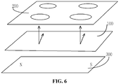
FIG. 6 is a schematic view of a qubit coupling system according to an embodiment of the present application. - In the drawings:
magnetic film material 100 first spin 101 second spin 102 superconducting- qubit array 200 first qubit 201 second qubit 202 driving apparatus 300 - The object, features and advantages of the present application will be more apparent from the detailed description of the present application in conjunction with the drawings. Details are set forth below to facilitate a thorough understanding of the present application. However, the present disclosure can be implemented in many modes different from the embodiments described herein, and those skilled in the art can make similar modifications without departing from the connotation of the present application, so the present application is not limited by the embodiments described below.
- Referring to
FIG. 1 , the present application provides a method for coupling any two qubits from among multiple superconducting qubits. The method is applicable to an occasion provided with a multi-superconducting-qubit array 200 and amagnetic film material 100 capable of implementing spin waves. The method includes the steps described below. - In S100, the
magnetic film material 100 is disposed below the multi-superconducting-qubit array 200. - In S200, multiple spin wave channels through which the spin waves pass are formed through a combination of magnetization directions of magnetic domains in the
magnetic film material 100. - In S300, multiple qubits of the multi-superconducting-qubit array (200) are disposed above the multiple spin wave channels through which the spin waves pass correspondingly, so that a coupling between each qubit and the spin waves is implemented.
- In S400, at least two qubits are disposed above one spin-wave channel, and a coupling between the at least two qubits is implemented through the coupling between the each of the at least two qubits and the spin waves.
- In S100, the
magnetic film material 100 is disposed below the multi-superconducting-qubit array 200 in the vertical direction, so that the multiple qubits of multi-superconducting-qubit array 200 are coupled through themagnetic film material 100. - The multi-superconducting-
qubit array 200 is composed of the multiple qubits. The multiple qubits are formed by multiple qubit coils. The state of each qubit coil is separately controlled by an additional wire. Themagnetic film material 100 is used for forming the multiple spin wave channels. The magnetic film material (100) may be divided into multiple elements. Each element is one magnetic domain. The magnetization direction of the magnetic domain of the each element may be separately controlled. - Specifically, referring to
FIG. 2 , in the magnetic material, due to the competition between an exchange effect, anisotropy of a magnetic crystal and a magnetic dipole-dipole interaction, in a system, in order to reduce the total energy, small magnetized regions having different directions will spontaneously be formed, which is so-called the magnetic domains, while the transition region of adjacent magnetic domains is a magnetic domain wall. Theoretical calculation shows that the spin waves have a bound-state solution in the magnetic domain wall, and the energy gap of this spin wave mode is zero in the case where only the exchange effect and the anisotropy of the magnetic crystal are considered. Due to this feature, the magnetic domain wall can serve as a spin wave channel for conducting the spin waves. - In S200, the multiple spin wave channels through which the spin waves pass are formed through the combination of magnetization directions of the magnetic domains in the
magnetic film material 100. Themagnetic film material 100 is provided with multiple magnetic domain elements. The multiple magnetic domain elements have their respective magnetization directions. The transition region of adjacent magnetic domain elements forms the magnetic domain wall, that is, the spin wave channel of the present application, for conducting one or more spin waves. - Furthermore, the formation of the magnetic domains may be controlled through the applied magnetic field, and whether the directions of the adjacent magnetic domains are the same or different can determine whether the magnetic domain wall exists between the magnetic domains. Only when the magnetization directions between adjacent magnetic domain elements are different, does the magnetic domain wall, that is, the spin wave channel, exist. Otherwise, no domain wall exists. The layout of the magnetic domain wall varies with the arrangement of the magnetic domains, thus any spin wave wiring mode can be obtained through editing of the arrangement of the magnetic domains and reconstruction can be performed between the magnetic domains.
- Specifically, a driving
apparatus 300 is disposed below themagnetic film material 100. The apparatus is used for applying the magnetic field to themagnetic film material 100 to drive one or more spin waves in the magnetic domain wall, that is, the spin wave channel. - In one embodiment, the driving
apparatus 300 disposed below themagnetic film material 100 is a circuit board with a specific wiring mode. - In S300, the multiple qubits of the multi-superconducting-
qubit array 200 are disposed above the multiple spin wave channels through which the spin waves pass correspondingly, so that the coupling between the each qubit and the spin waves is implemented. - Referring to
FIGS. 3 and4 , the multiple qubit coils of the multi-superconducting-qubit array 200 are disposed above the spin wave channel, so that the coupling between the spin waves in the spin wave channel and the each qubit is implemented. A path along which the spin waves can travel is defined through an adjustment to the combination of the magnetization directions of the magnetic domain elements in themagnetic film material 100, so that the multiple superconducting qubits above the path can be connected through the spin waves so as to be coupled. - In S400, at least two qubits are disposing above one spin wave channel, and the coupling between the at least two qubits is implemented through the coupling between the each of the at least two qubits and the spin waves.
- Referring to
FIG. 3 , a spin wave channel includes at least afirst spin 101 and asecond spin 102. Thefirst spin 101 correspondingly acts on afirst qubit 201 of the multi-superconducting-qubit array 200. Thesecond spin 102 correspondingly acts on asecond qubit 202 of the multi-superconducting-qubit array 200. Further, the coupling between thefirst spin 101 and thefirst qubit 201 is implemented and the coupling between thesecond spin 102 and thesecond qubit 202 is implemented. - In one embodiment, after the coupling between the
first spin 101 and thefirst qubit 201 is implemented and the coupling between thesecond spin 102 and thesecond qubit 202 is implemented, the state change of thefirst qubit 201 in the superconducting qubit layer acts on thefirst spin 101 of the spin waves through inter-layer coupling, and then the state change is transferred to thesecond spin 102 through the spin waves traveling along the specific path of the spin wave channel. After that, the state change acts on thesecond qubit 202 through the interlayer coupling. In this way, the coupling between thefirst spin 101 and thesecond spin 102 is established, and at the same time, the coupling between thefirst qubit 201 and thesecond qubit 202 is also established. The traveling path of the spin waves, that is, the path of the spin wave channel, may be controlled through the adjustment to the combination of the magnetization directions of the magnetic domains in themagnetic film material 100, so that the coupling between any two qubits can be implemented. - In one embodiment, one qubit may be coupled to at least one spin wave and may be coupled to the multiple spin waves.
- Referring to
FIG. 4 , in one embodiment, a single qubit coil generates the magnetic field to act on the spins in the spin wave channel. When the radius R = 1 µm and the superconducting critical current I = 100 nanoamps in one coil, the magnetic field at the center of the coil is about 0.001 gauss. Such a magnetic field generates about 1 electronvolt of energy on a single spin. When themagnetic film material 100 is disposed below the superconducting qubit coil, the single superconducting qubit coil can accommodate 1 million to 10 million spins, the total energy of the superconducting qubit coil can reach 1 micro-electronvolt to 10 micro-electronvolts that are close to the energy level difference between two quantum states of one superconducting qubit. Therefore, the coupling between the superconducting qubit coil and themagnetic film material 100 can change the state of the superconducting qubit. It is also known that the energy amplitude of a spin wave is within 3000 micro-electronvolts to 10000 micro-electronvolts that are much greater than the coupling energy and is capable of transferring this coupling energy. - Further, the magnitude of the coupling energy may be adjusted through: (1) an adjustment to the number density of the spin in the magnetic domains in the
magnetic film material 100, (2) an adjustment to the distance between the multiple superconducting qubit coils and themagnetic film material 100, and (3) an adjustment to the magnetization directions or magnetization intensities of the magnetic domains in themagnetic film material 100. - Referring to
FIG. 5 , in one embodiment, as the distance between the plane in which the multiple superconducting qubit coils are located and the plane in which the spin waves are located increases, the interaction between the multiple qubit coils and the spin waves will decay rapidly, so the magnitude of the interaction can be adjusted through the vertical distance between the multiple superconducting qubit coils and the magnetic film material. - In one embodiment, the magnetization directions of ferromagnetic domains on both sides of one spin wave channel, which is covered by superconducting qubit coils, are opposite, so the overall magnetic flux is zero and the superconductivity will not be destroyed. For the same purpose, the ferromagnetic magnetic domains may be replaced by antiferromageic domains, so that the superconductivity can be prevented from being destroyed by the high magnetic field.
- According to the method for coupling any two qubits from among the multiple superconducting qubits provided in the present application, a structure where a superconducting qubit layer is disposed in an upper layer and a
magnetic film material 100 layer is disposed in a lower layer along the vertical direction respectively is adopted, and the state change of the multiple qubits of the superconducting qubit layer is transferred through the spin waves of themagnetic film material 100 layer. Finally, the coupling between any two superconducting qubits is implemented through both the soft connection of the spin waves, and the coupling between the each superconducting qubit and the spin waves. At the same time, the magnitude of the coupling energy can be adjusted according to multiple methods, for example, the adjustment to the number density of the spin in the magnetic domains in themagnetic film material 100, the adjustment to the distance between the multiple superconducting qubit coils and themagnetic film material 100, the adjustment to the magnetization directions or magnetization intensities of the magnetic domains in themagnetic film material 100, or the like. Moreover, the traveling path of the spin wave channel can be changed through an adjustment to the distribution of the multiple magnetic domain elements, so that the coupling between any two superconducting qubits is further implemented. - Referring to
FIG. 6 , the present application provides a qubit coupling system. The system is provided with a multi-superconducting-qubit array 200, amagnetic film material 100 and adriving apparatus 300 sequentially along the vertical direction. The drivingapparatus 300 is used for applying a magnetic field to the magnetic film material to drive spin waves in a spin-wave channel. - The multi-superconducting-
qubit array 200 is composed of multiple qubits. The multiple qubits are formed by multiple qubit coils. The state of each qubit coil is separately controlled by an additional wire. Themagnetic film material 100 is used for forming the spin wave channel. Themagnetic film material 100 may be divided into multiple elements. Each element is one magnetic domain. The magnetization direction of the magnetic domain of the each element may be separately controlled. - In one embodiment, the
magnetic film material 100 is used for forming the spin wave channel. Themagnetic film material 100 may be divided into multiple elements. Each element is one magnetic domain. The magnetization direction of the magnetic domain of the each element may be separately controlled. In the magnetic material, due to the competition between an exchange effect, anisotropy of a magnetic crystal and a magnetic dipole-dipole interaction, in a system, in order to reduce the total energy, small magnetized regions having different directions will spontaneously be formed, which is so-called the magnetic domains, while the transition region of adjacent magnetic domains is a magnetic domain wall. Theoretical calculation shows that the spin waves have a bound-state solution in the magnetic domain wall, and the energy gap of the spin wave mode is zero in the case where only the exchange effect and the anisotropy of the magnetic crystal are considered. Due to this feature, the magnetic domain wall can serve as a spin wave channel for conducting the spin waves. Magnetization directions of the spin waves are perpendicular to the multiple superconducting qubit coils as shown inFIGS. 3 ,4 and6 . It is to be noted that the magnetization directions of the spin waves may be parallel to the multiple superconducting qubit coils, as long as the coupling effect between the spin waves and the multiple superconducting qubit coils can be generated. - In one embodiment, a structural modification between adjacent magnetic domains, may be performed by using a manual method, for example, fabricating a trench or the like to pin the magnetic-domain wall to the boundary of the magnetic-domains.
- In one embodiment, the formation and the magnetization direction of magnetic domains may be controlled through the applied magnetic field, and whether the magnetization directions of adjacent magnetic domains are the same or different can determine whether the magnetic domain wall exists between the magnetic domains. Only when the magnetization directions between adjacent magnetic-domain elements are different, does the magnetic domain wall, that is, the spin-wave channel, exists. Otherwise, no domain wall exists. The layout of the magnetic-domain wall varies with the arrangement of the magnetic domains, thus any spin-wave wiring mode can be obtained through editing of the arrangement of the magnetic domains and reconstruction can be performed between the magnetic domains.
- In one embodiment, the driving
apparatus 300 disposed below themagnetic film material 100 is a circuit board with a specific wiring mode, and is used for applying the magnetic field to the magnetic film material to drive one or more spin waves in the magnetic domain wall, that is, the spin wave channel. - In one embodiment, when the anisotropy of the magnetic crystal is uniaxial anisotropy, only a 180-degree magnetic domain wall exists in the material; and when the anisotropy of the magnetic crystal is biaxial or cubic anisotropy, a 90-degree or 180-degree magnetic domain wall exists in the material. A material with higher-fold symmetry may have more types of magnetic-domain walls.
- In one embodiment, after the coupling between a
first spin 101 and afirst qubit 201 is implemented and the coupling between asecond spin 102 and asecond qubit 202 is implemented, the state change of thefirst qubit 201 in the superconducting qubit layer acts on thefirst spin 101 of the spin waves through interlayer coupling, and then the state change is transferred to thesecond spin 102 through the spin-wave traveling along the specific path of the spin wave channel. After that, the state change acts on thesecond qubit 202 through the inter-layer coupling. In this way, the coupling between thefirst spin 101 and thesecond spin 102 is established, and at the same time, the interaction between thefirst qubit 201 and thesecond qubit 202 is also established. The traveling path of the spin waves, that is, the path of the spin wave channel, may be controlled through the adjustment to the combination of the magnetization directions of the magnetic domains in themagnetic film material 100, so that the coupling between any two qubits can be implemented. - In one embodiment, each qubit may be coupled to at least one spin wave and may be coupled to multiple spin waves.
- The qubit coupling system provided in the present application adopts a structure where the superconducting qubit layer and the
magnetic film material 100 layer are disposed in an upper layer and a lower layer respectively along the vertical direction. In the system, the drivingapparatus 300 is used for applying the magnetic field to the magnetic film material to drive one or more spin waves in the magnetic domain wall, that is, the spin wave channel. In the system, the state change of the multiple qubits of the superconducting qubit layer is transferred through the spin waves of themagnetic film material 100 layer. The coupling between any two superconducting qubits is implemented through both the soft connection of the spin waves, and the coupling between the each superconducting qubit and the spin waves. At the same time, the magnitude of the coupling energy may be adjusted according to multiple methods, for example, an adjustment to the number density of spins in the magnetic domains in themagnetic film material 100, an adjustment to the distance between the multiple superconducting qubit coils and themagnetic film material 100, an adjustment to the magnetization directions or magnetization intensities of the magnetic domains in themagnetic film material 100, or the like. Moreover, the traveling path of the spin wave channel can be changed through an adjustment to the distribution mode of multiple magnetic domain elements, so that the coupling between any two superconducting qubits is further implemented. - The technical features of the above embodiments may be combined in any way. For conciseness, not all possible combinations of the technical features in the above embodiments are described. However, as long as the combinations of these technical features do not conflict, these combinations should be considered to be within the scope of the specification.
- The above embodiments are merely several embodiments of the present application. These embodiments are described in a specific and detailed manner but cannot be understood as a limit to the scope of the present application. It is to be noted that for those skilled in the art, a number of improvements and modifications can be made without departing from the concept of the present disclosure, and these improvements and modifications are within the scope of the present disclosure. Therefore, the scope of the present disclosure is defined by the appended claims.
Claims (9)
- A method for coupling any two qubits from among a plurality of superconducting qubits, which is applied to an occasion provided with a multi-superconducting-qubit array (200) and a magnetic film material (100) capable of implementing spin waves, the method comprising:disposing the magnetic film material (100) below the multi-superconducting-qubit array (200);forming, through a combination of magnetization directions of magnetic domains in the magnetic film material (100), a plurality of channels through which the spin waves pass;disposing a plurality of qubits of the multi-superconducting-qubit array (200) above the plurality of channels through which the spin waves pass correspondingly to implement a coupling between each of the plurality of qubits and the spin waves; anddisposing at least two of the plurality of qubits above one of the plurality of channels, and implementing a coupling between the at least two of the plurality of qubits through the coupling between the each of the at least two of the plurality of qubits and the spin waves.
- The method for coupling any two qubits from among the plurality of superconducting qubits according to claim 1, further comprising:
changing the plurality of channels through which the spin waves pass by changing the combination of the magnetization directions of the magnetic domains in the magnetic film material (100). - The method for coupling any two qubits from among the plurality of superconducting qubits according to claim 1, wherein
the spin waves at least comprise a first spin (101) and a second spin (102);
the first spin (101) correspondingly acts on a first qubit (201) of the multi-superconducting-qubit array (200); and
the second spin (102) correspondingly acts on a second qubit (202) of the multi-superconducting-qubit array (200) - The method for coupling any two qubits from among the plurality of superconducting qubits according to claim 3, further comprising:implementing coupling between the first spin (101) and the first qubit (201);implementing coupling between the second spin (102) and the second qubit (202); andimplementing coupling between the first qubit (201) and the second qubit (202) through the spin waves.
- The method for coupling any two qubits from among the plurality of superconducting qubits according to claim 4, further comprising:
adjusting coupling energy of a plurality of superconducting qubit coils and the spin waves by adjusting a number density of the first spin (101) of the spin waves and a number density of the second spin (102) of the spin waves. - The method for coupling any two qubits from among the plurality of superconducting qubits according to claim 5, further comprising:
adjusting the coupling energy of the plurality of superconducting qubit coils and the spin waves by adjusting a vertical distance between the plurality of superconducting qubit coils and magnetic film material (100). - The method for coupling any two qubits from among the plurality of superconducting qubits according to claim 5, further comprising:
adjusting the coupling energy of the plurality of superconducting qubit coils and the spin waves by adjusting magnetization directions or magnetization intensities of the magnetic domains in the magnetic film material (100). - A qubit coupling system, comprising:a multi-superconducting-qubit array (200), which comprises a plurality of qubit coils;a magnetic film material (100), which is configured to form a plurality of spin wave channels by using magnetic domain walls between magnetic domains as waveguides; anda driving apparatus (300), which is configured to apply a magnetic field to the magnetic film material to drive spin waves in the plurality of spin wave channels,wherein the multi-superconducting-qubit array (200), the magnetic film material (100) and the driving apparatus (300) are sequentially disposed along a vertical direction.
- The qubit coupling system according to claim 8, wherein the magnetic film material (100) is divided into a plurality of magnetic-domain elements and magnetization directions of the plurality of magnetic-domain elements are changed through the driving apparatus.
Applications Claiming Priority (2)
| Application Number | Priority Date | Filing Date | Title |
|---|---|---|---|
| CN201810380235.6A CN109583592B (en) | 2018-04-25 | 2018-04-25 | Method and system for coupling any two bits in multiple superconducting qubits |
| PCT/CN2019/076924 WO2019205810A1 (en) | 2018-04-25 | 2019-03-05 | Method and system for coupling any two bits from among multiple superconductor quantum bits |
Publications (4)
| Publication Number | Publication Date |
|---|---|
| EP3786858A1 true EP3786858A1 (en) | 2021-03-03 |
| EP3786858A4 EP3786858A4 (en) | 2022-02-16 |
| EP3786858C0 EP3786858C0 (en) | 2025-08-27 |
| EP3786858B1 EP3786858B1 (en) | 2025-08-27 |
Family
ID=65919538
Family Applications (1)
| Application Number | Title | Priority Date | Filing Date |
|---|---|---|---|
| EP19792154.7A Active EP3786858B1 (en) | 2018-04-25 | 2019-03-05 | Method and system for coupling any two bits from among multiple superconductor quantum bits |
Country Status (5)
| Country | Link |
|---|---|
| US (1) | US12093781B2 (en) |
| EP (1) | EP3786858B1 (en) |
| JP (1) | JP6971333B2 (en) |
| CN (1) | CN109583592B (en) |
| WO (1) | WO2019205810A1 (en) |
Families Citing this family (8)
| Publication number | Priority date | Publication date | Assignee | Title |
|---|---|---|---|---|
| SG11201803545QA (en) * | 2015-10-29 | 2018-05-30 | Google Llc | Removing leakage in a quantum bit |
| CN111048894B (en) * | 2019-12-13 | 2022-06-03 | 电子科技大学 | Spintronic antenna array based on inverse spin Hall effect and its fabrication method |
| JP7516085B2 (en) * | 2020-03-25 | 2024-07-16 | 株式会社神戸製鋼所 | Quantum bit integration device |
| US20240371540A1 (en) * | 2021-04-23 | 2024-11-07 | University Of Pittsburgh - Of The Commonwealth System Of Higher Education | Systems and methods for assembling electron spin and charge to possess properties of a magnetic monopole |
| AU2022289736A1 (en) | 2021-06-11 | 2024-02-01 | Caleb JORDAN | System and method of flux bias for superconducting quantum circuits |
| CN114528021B (en) * | 2022-01-28 | 2022-11-08 | 中国人民解放军战略支援部队信息工程大学 | Time-sharing multiplexing quantum measurement and control system and low-power-consumption high-efficiency quantum measurement and control compiling method |
| CN115659905B (en) * | 2022-10-24 | 2023-06-30 | 北京百度网讯科技有限公司 | Method and device for determining coupling strength between quantum devices in superconducting quantum chip layout |
| KR20240176336A (en) | 2023-06-15 | 2024-12-24 | 삼성전자주식회사 | Superconducting qubit using ferromagnet and superconducting qubit-based device including the same |
Family Cites Families (21)
| Publication number | Priority date | Publication date | Assignee | Title |
|---|---|---|---|---|
| JP4714918B2 (en) | 2002-11-29 | 2011-07-06 | 独立行政法人科学技術振興機構 | Spin injection device and magnetic device using spin injection device |
| US7212026B2 (en) * | 2004-10-29 | 2007-05-01 | Intel Corporation | Spin-orbital quantum cellular automata logic devices and systems |
| US7528456B1 (en) * | 2005-03-01 | 2009-05-05 | The Regents Of The University Of California | Nano-scale computational architectures with spin wave bus |
| US7898282B2 (en) * | 2005-04-26 | 2011-03-01 | D-Wave Systems Inc. | Systems, devices, and methods for controllably coupling qubits |
| US7535070B2 (en) * | 2006-01-30 | 2009-05-19 | The Regents Of The University Of California | Spin-wave architectures |
| US8183652B2 (en) * | 2007-02-12 | 2012-05-22 | Avalanche Technology, Inc. | Non-volatile magnetic memory with low switching current and high thermal stability |
| US9228968B2 (en) * | 2010-03-25 | 2016-01-05 | Nec Corporation | Thermal sensor and platform |
| JP5673951B2 (en) | 2011-08-23 | 2015-02-18 | 独立行政法人産業技術総合研究所 | Field ferromagnetic resonance excitation method and magnetic functional element using the same |
| US9129679B2 (en) * | 2012-09-05 | 2015-09-08 | Kabushiki Kaisha Toshiba | Shift register type magnetic memory |
| WO2014207818A1 (en) * | 2013-06-25 | 2014-12-31 | 株式会社日立製作所 | Spin wave circuit |
| JP5649704B1 (en) * | 2013-09-18 | 2015-01-07 | 株式会社東芝 | Magnetic recording device |
| US9767876B2 (en) * | 2014-10-28 | 2017-09-19 | The Regents Of The University Of California | Magnonic holographic memory and methods |
| AU2015252051B2 (en) * | 2014-11-03 | 2020-10-15 | Newsouth Innovations Pty Limited | A quantum processor |
| CN105070824B (en) * | 2015-07-30 | 2017-07-28 | 复旦大学 | A kind of restructural spin wave network of conductors based on neticdomain wall |
| FI20165312A (en) * | 2016-04-12 | 2017-10-13 | Aalto-Korkeakoulusäätiö Sr | Magnon element and related procedure |
| US9711201B1 (en) * | 2016-05-19 | 2017-07-18 | Uchicago Argonne, Llc | Reconfigurable and writable magnetic charge crystals |
| US10217522B2 (en) * | 2016-05-23 | 2019-02-26 | Regents Of The University Of Minnesota | Fast magnetoelectric device based on current-driven domain wall propagation |
| US10361292B2 (en) * | 2017-02-17 | 2019-07-23 | Intel Corporation | Magneto-electric logic devices using semiconductor channel with large spin-orbit coupling |
| CN107564868B (en) * | 2017-07-07 | 2019-08-02 | 清华大学 | An integrated packaging structure and method for a superconducting quantum computing chip |
| CN107204813A (en) * | 2017-07-28 | 2017-09-26 | 浙江九州量子信息技术股份有限公司 | A kind of phase code device based on silicon substrate integrated waveguide |
| CN206977434U (en) | 2017-07-28 | 2018-02-06 | 浙江九州量子信息技术股份有限公司 | A kind of phase code device based on silicon substrate integrated waveguide |
-
2018
- 2018-04-25 CN CN201810380235.6A patent/CN109583592B/en active Active
-
2019
- 2019-03-05 JP JP2019567584A patent/JP6971333B2/en active Active
- 2019-03-05 US US16/757,680 patent/US12093781B2/en active Active
- 2019-03-05 EP EP19792154.7A patent/EP3786858B1/en active Active
- 2019-03-05 WO PCT/CN2019/076924 patent/WO2019205810A1/en not_active Ceased
Also Published As
| Publication number | Publication date |
|---|---|
| EP3786858C0 (en) | 2025-08-27 |
| JP6971333B2 (en) | 2021-11-24 |
| US12093781B2 (en) | 2024-09-17 |
| EP3786858A4 (en) | 2022-02-16 |
| WO2019205810A1 (en) | 2019-10-31 |
| US20200250567A1 (en) | 2020-08-06 |
| CN109583592B (en) | 2020-04-17 |
| EP3786858B1 (en) | 2025-08-27 |
| JP2020528662A (en) | 2020-09-24 |
| CN109583592A (en) | 2019-04-05 |
Similar Documents
| Publication | Publication Date | Title |
|---|---|---|
| EP3786858B1 (en) | Method and system for coupling any two bits from among multiple superconductor quantum bits | |
| US11010684B2 (en) | Quantum spin hall-based charging energy-protected quantum computation | |
| US10235634B1 (en) | Magnetic flux control in superconducting device | |
| US12333383B2 (en) | Additive control of qubits for enabling time-domain and frequency-domain mutiplexing | |
| US12340273B2 (en) | Quantum processor unit architecture for quantum computing via an arbitrarily programmable interaction connectivity graph | |
| JP7658981B2 (en) | Systems and methods for scalable quantum computing | |
| US7898282B2 (en) | Systems, devices, and methods for controllably coupling qubits | |
| DE112012002442B4 (en) | Magnetic storage system and method in various modes of operation | |
| CN214378496U (en) | Quantum chip | |
| US11024791B1 (en) | Magnetically stabilized magnetic Josephson junction memory cell | |
| US4837604A (en) | Femtosecond three-terminal switch and vertical tunnel junction | |
| Khitun et al. | Magnonic logic devices | |
| EP4195290A1 (en) | Qubit array device | |
| Gallagher et al. | Superconductivity at IBM–a centennial review: part I–superconducting computer and device applications | |
| EP4594951A1 (en) | Quantum computing arrangement and quantum computer | |
| JP2543374B2 (en) | Magnetic artificial lattice film | |
| CN120373480A (en) | Efficient general quantum computer central processing unit and operating method thereof | |
| WO2025009053A1 (en) | Quantum converter and quantum conversion method | |
| CN119340044A (en) | Three-dimensional axion insulator, multi-port isolator and design method thereof | |
| Yu et al. | 6. Short Wavelength Magnonics | |
| HK40056556A (en) | Additive control of qubits for enabling time-domain and frequency-domain multiplexing | |
| Biderang et al. | Momentum space imaging of locally noncentrosymmetric superconductors | |
| De Long et al. | Size and interface effects in patterned magnetic and superconducting thin films | |
| Akaike et al. | The Effect of Magnetic Nanoparticles on Inductances for SFQ Device Application | |
| JPH02181983A (en) | Superconducting tunnel junction element |
Legal Events
| Date | Code | Title | Description |
|---|---|---|---|
| STAA | Information on the status of an ep patent application or granted ep patent |
Free format text: STATUS: THE INTERNATIONAL PUBLICATION HAS BEEN MADE |
|
| PUAI | Public reference made under article 153(3) epc to a published international application that has entered the european phase |
Free format text: ORIGINAL CODE: 0009012 |
|
| STAA | Information on the status of an ep patent application or granted ep patent |
Free format text: STATUS: REQUEST FOR EXAMINATION WAS MADE |
|
| 17P | Request for examination filed |
Effective date: 20200330 |
|
| AK | Designated contracting states |
Kind code of ref document: A1 Designated state(s): AL AT BE BG CH CY CZ DE DK EE ES FI FR GB GR HR HU IE IS IT LI LT LU LV MC MK MT NL NO PL PT RO RS SE SI SK SM TR |
|
| AX | Request for extension of the european patent |
Extension state: BA ME |
|
| DAV | Request for validation of the european patent (deleted) | ||
| DAX | Request for extension of the european patent (deleted) | ||
| A4 | Supplementary search report drawn up and despatched |
Effective date: 20220114 |
|
| RIC1 | Information provided on ipc code assigned before grant |
Ipc: G06N 10/00 20190101AFI20220110BHEP |
|
| REG | Reference to a national code |
Ref legal event code: R079 Free format text: PREVIOUS MAIN CLASS: G06N0010000000 Ipc: G06N0010400000 Ref country code: DE Ref document number: 602019074804 Country of ref document: DE |
|
| GRAP | Despatch of communication of intention to grant a patent |
Free format text: ORIGINAL CODE: EPIDOSNIGR1 |
|
| STAA | Information on the status of an ep patent application or granted ep patent |
Free format text: STATUS: GRANT OF PATENT IS INTENDED |
|
| RIC1 | Information provided on ipc code assigned before grant |
Ipc: H10N 69/00 20230101ALN20250320BHEP Ipc: H10N 50/20 20230101ALN20250320BHEP Ipc: G06N 10/40 20220101AFI20250320BHEP |
|
| INTG | Intention to grant announced |
Effective date: 20250326 |
|
| GRAS | Grant fee paid |
Free format text: ORIGINAL CODE: EPIDOSNIGR3 |
|
| GRAA | (expected) grant |
Free format text: ORIGINAL CODE: 0009210 |
|
| STAA | Information on the status of an ep patent application or granted ep patent |
Free format text: STATUS: THE PATENT HAS BEEN GRANTED |
|
| AK | Designated contracting states |
Kind code of ref document: B1 Designated state(s): AL AT BE BG CH CY CZ DE DK EE ES FI FR GB GR HR HU IE IS IT LI LT LU LV MC MK MT NL NO PL PT RO RS SE SI SK SM TR |
|
| REG | Reference to a national code |
Ref country code: GB Ref legal event code: FG4D |
|
| REG | Reference to a national code |
Ref country code: CH Ref legal event code: EP |
|
| REG | Reference to a national code |
Ref country code: DE Ref legal event code: R096 Ref document number: 602019074804 Country of ref document: DE |
|
| REG | Reference to a national code |
Ref country code: IE Ref legal event code: FG4D |
|
| U01 | Request for unitary effect filed |
Effective date: 20250924 |
|
| U07 | Unitary effect registered |
Designated state(s): AT BE BG DE DK EE FI FR IT LT LU LV MT NL PT RO SE SI Effective date: 20251006 |
|
| PG25 | Lapsed in a contracting state [announced via postgrant information from national office to epo] |
Ref country code: IS Free format text: LAPSE BECAUSE OF FAILURE TO SUBMIT A TRANSLATION OF THE DESCRIPTION OR TO PAY THE FEE WITHIN THE PRESCRIBED TIME-LIMIT Effective date: 20251227 |
|
| PG25 | Lapsed in a contracting state [announced via postgrant information from national office to epo] |
Ref country code: NO Free format text: LAPSE BECAUSE OF FAILURE TO SUBMIT A TRANSLATION OF THE DESCRIPTION OR TO PAY THE FEE WITHIN THE PRESCRIBED TIME-LIMIT Effective date: 20251127 |
|
| PG25 | Lapsed in a contracting state [announced via postgrant information from national office to epo] |
Ref country code: HR Free format text: LAPSE BECAUSE OF FAILURE TO SUBMIT A TRANSLATION OF THE DESCRIPTION OR TO PAY THE FEE WITHIN THE PRESCRIBED TIME-LIMIT Effective date: 20250827 |
|
| PG25 | Lapsed in a contracting state [announced via postgrant information from national office to epo] |
Ref country code: GR Free format text: LAPSE BECAUSE OF FAILURE TO SUBMIT A TRANSLATION OF THE DESCRIPTION OR TO PAY THE FEE WITHIN THE PRESCRIBED TIME-LIMIT Effective date: 20251128 |
|
| PG25 | Lapsed in a contracting state [announced via postgrant information from national office to epo] |
Ref country code: PL Free format text: LAPSE BECAUSE OF FAILURE TO SUBMIT A TRANSLATION OF THE DESCRIPTION OR TO PAY THE FEE WITHIN THE PRESCRIBED TIME-LIMIT Effective date: 20250827 |
|
| PG25 | Lapsed in a contracting state [announced via postgrant information from national office to epo] |
Ref country code: RS Free format text: LAPSE BECAUSE OF FAILURE TO SUBMIT A TRANSLATION OF THE DESCRIPTION OR TO PAY THE FEE WITHIN THE PRESCRIBED TIME-LIMIT Effective date: 20251127 |
|
| PG25 | Lapsed in a contracting state [announced via postgrant information from national office to epo] |
Ref country code: ES Free format text: LAPSE BECAUSE OF FAILURE TO SUBMIT A TRANSLATION OF THE DESCRIPTION OR TO PAY THE FEE WITHIN THE PRESCRIBED TIME-LIMIT Effective date: 20250827 |
|
| PG25 | Lapsed in a contracting state [announced via postgrant information from national office to epo] |
Ref country code: SM Free format text: LAPSE BECAUSE OF FAILURE TO SUBMIT A TRANSLATION OF THE DESCRIPTION OR TO PAY THE FEE WITHIN THE PRESCRIBED TIME-LIMIT Effective date: 20250827 |
|
| PG25 | Lapsed in a contracting state [announced via postgrant information from national office to epo] |
Ref country code: CZ Free format text: LAPSE BECAUSE OF FAILURE TO SUBMIT A TRANSLATION OF THE DESCRIPTION OR TO PAY THE FEE WITHIN THE PRESCRIBED TIME-LIMIT Effective date: 20250827 |
|
| PG25 | Lapsed in a contracting state [announced via postgrant information from national office to epo] |
Ref country code: SK Free format text: LAPSE BECAUSE OF FAILURE TO SUBMIT A TRANSLATION OF THE DESCRIPTION OR TO PAY THE FEE WITHIN THE PRESCRIBED TIME-LIMIT Effective date: 20250827 |