EP3786694A1 - Display apparatus - Google Patents
Display apparatus Download PDFInfo
- Publication number
- EP3786694A1 EP3786694A1 EP20193843.8A EP20193843A EP3786694A1 EP 3786694 A1 EP3786694 A1 EP 3786694A1 EP 20193843 A EP20193843 A EP 20193843A EP 3786694 A1 EP3786694 A1 EP 3786694A1
- Authority
- EP
- European Patent Office
- Prior art keywords
- opening portion
- layer
- supporting member
- display apparatus
- display
- Prior art date
- Legal status (The legal status is an assumption and is not a legal conclusion. Google has not performed a legal analysis and makes no representation as to the accuracy of the status listed.)
- Granted
Links
Images




Classifications
-
- H—ELECTRICITY
- H10—SEMICONDUCTOR DEVICES; ELECTRIC SOLID-STATE DEVICES NOT OTHERWISE PROVIDED FOR
- H10K—ORGANIC ELECTRIC SOLID-STATE DEVICES
- H10K59/00—Integrated devices, or assemblies of multiple devices, comprising at least one organic light-emitting element covered by group H10K50/00
- H10K59/10—OLED displays
- H10K59/12—Active-matrix OLED [AMOLED] displays
-
- H—ELECTRICITY
- H10—SEMICONDUCTOR DEVICES; ELECTRIC SOLID-STATE DEVICES NOT OTHERWISE PROVIDED FOR
- H10K—ORGANIC ELECTRIC SOLID-STATE DEVICES
- H10K59/00—Integrated devices, or assemblies of multiple devices, comprising at least one organic light-emitting element covered by group H10K50/00
- H10K59/10—OLED displays
- H10K59/12—Active-matrix OLED [AMOLED] displays
- H10K59/122—Pixel-defining structures or layers, e.g. banks
-
- G—PHYSICS
- G02—OPTICS
- G02F—OPTICAL DEVICES OR ARRANGEMENTS FOR THE CONTROL OF LIGHT BY MODIFICATION OF THE OPTICAL PROPERTIES OF THE MEDIA OF THE ELEMENTS INVOLVED THEREIN; NON-LINEAR OPTICS; FREQUENCY-CHANGING OF LIGHT; OPTICAL LOGIC ELEMENTS; OPTICAL ANALOGUE/DIGITAL CONVERTERS
- G02F1/00—Devices or arrangements for the control of the intensity, colour, phase, polarisation or direction of light arriving from an independent light source, e.g. switching, gating or modulating; Non-linear optics
- G02F1/01—Devices or arrangements for the control of the intensity, colour, phase, polarisation or direction of light arriving from an independent light source, e.g. switching, gating or modulating; Non-linear optics for the control of the intensity, phase, polarisation or colour
- G02F1/13—Devices or arrangements for the control of the intensity, colour, phase, polarisation or direction of light arriving from an independent light source, e.g. switching, gating or modulating; Non-linear optics for the control of the intensity, phase, polarisation or colour based on liquid crystals, e.g. single liquid crystal display cells
- G02F1/133—Constructional arrangements; Operation of liquid crystal cells; Circuit arrangements
- G02F1/1333—Constructional arrangements; Manufacturing methods
-
- G—PHYSICS
- G09—EDUCATION; CRYPTOGRAPHY; DISPLAY; ADVERTISING; SEALS
- G09F—DISPLAYING; ADVERTISING; SIGNS; LABELS OR NAME-PLATES; SEALS
- G09F9/00—Indicating arrangements for variable information in which the information is built-up on a support by selection or combination of individual elements
- G09F9/30—Indicating arrangements for variable information in which the information is built-up on a support by selection or combination of individual elements in which the desired character or characters are formed by combining individual elements
- G09F9/301—Indicating arrangements for variable information in which the information is built-up on a support by selection or combination of individual elements in which the desired character or characters are formed by combining individual elements flexible foldable or roll-able electronic displays, e.g. thin LCD, OLED
-
- H—ELECTRICITY
- H04—ELECTRIC COMMUNICATION TECHNIQUE
- H04M—TELEPHONIC COMMUNICATION
- H04M1/00—Substation equipment, e.g. for use by subscribers
- H04M1/02—Constructional features of telephone sets
- H04M1/0202—Portable telephone sets, e.g. cordless phones, mobile phones or bar type handsets
- H04M1/026—Details of the structure or mounting of specific components
- H04M1/0264—Details of the structure or mounting of specific components for a camera module assembly
-
- H—ELECTRICITY
- H04—ELECTRIC COMMUNICATION TECHNIQUE
- H04M—TELEPHONIC COMMUNICATION
- H04M1/00—Substation equipment, e.g. for use by subscribers
- H04M1/02—Constructional features of telephone sets
- H04M1/0202—Portable telephone sets, e.g. cordless phones, mobile phones or bar type handsets
- H04M1/026—Details of the structure or mounting of specific components
- H04M1/0266—Details of the structure or mounting of specific components for a display module assembly
- H04M1/0268—Details of the structure or mounting of specific components for a display module assembly including a flexible display panel
-
- H—ELECTRICITY
- H05—ELECTRIC TECHNIQUES NOT OTHERWISE PROVIDED FOR
- H05K—PRINTED CIRCUITS; CASINGS OR CONSTRUCTIONAL DETAILS OF ELECTRIC APPARATUS; MANUFACTURE OF ASSEMBLAGES OF ELECTRICAL COMPONENTS
- H05K5/00—Casings, cabinets or drawers for electric apparatus
- H05K5/02—Details
- H05K5/03—Covers
-
- H—ELECTRICITY
- H10—SEMICONDUCTOR DEVICES; ELECTRIC SOLID-STATE DEVICES NOT OTHERWISE PROVIDED FOR
- H10K—ORGANIC ELECTRIC SOLID-STATE DEVICES
- H10K59/00—Integrated devices, or assemblies of multiple devices, comprising at least one organic light-emitting element covered by group H10K50/00
-
- H—ELECTRICITY
- H10—SEMICONDUCTOR DEVICES; ELECTRIC SOLID-STATE DEVICES NOT OTHERWISE PROVIDED FOR
- H10K—ORGANIC ELECTRIC SOLID-STATE DEVICES
- H10K59/00—Integrated devices, or assemblies of multiple devices, comprising at least one organic light-emitting element covered by group H10K50/00
- H10K59/10—OLED displays
- H10K59/12—Active-matrix OLED [AMOLED] displays
- H10K59/121—Active-matrix OLED [AMOLED] displays characterised by the geometry or disposition of pixel elements
- H10K59/1213—Active-matrix OLED [AMOLED] displays characterised by the geometry or disposition of pixel elements the pixel elements being TFTs
-
- H—ELECTRICITY
- H10—SEMICONDUCTOR DEVICES; ELECTRIC SOLID-STATE DEVICES NOT OTHERWISE PROVIDED FOR
- H10K—ORGANIC ELECTRIC SOLID-STATE DEVICES
- H10K59/00—Integrated devices, or assemblies of multiple devices, comprising at least one organic light-emitting element covered by group H10K50/00
- H10K59/10—OLED displays
- H10K59/12—Active-matrix OLED [AMOLED] displays
- H10K59/121—Active-matrix OLED [AMOLED] displays characterised by the geometry or disposition of pixel elements
- H10K59/1216—Active-matrix OLED [AMOLED] displays characterised by the geometry or disposition of pixel elements the pixel elements being capacitors
-
- H—ELECTRICITY
- H10—SEMICONDUCTOR DEVICES; ELECTRIC SOLID-STATE DEVICES NOT OTHERWISE PROVIDED FOR
- H10K—ORGANIC ELECTRIC SOLID-STATE DEVICES
- H10K59/00—Integrated devices, or assemblies of multiple devices, comprising at least one organic light-emitting element covered by group H10K50/00
- H10K59/10—OLED displays
- H10K59/12—Active-matrix OLED [AMOLED] displays
- H10K59/123—Connection of the pixel electrodes to the thin film transistors [TFT]
-
- H—ELECTRICITY
- H10—SEMICONDUCTOR DEVICES; ELECTRIC SOLID-STATE DEVICES NOT OTHERWISE PROVIDED FOR
- H10K—ORGANIC ELECTRIC SOLID-STATE DEVICES
- H10K59/00—Integrated devices, or assemblies of multiple devices, comprising at least one organic light-emitting element covered by group H10K50/00
- H10K59/10—OLED displays
- H10K59/12—Active-matrix OLED [AMOLED] displays
- H10K59/131—Interconnections, e.g. wiring lines or terminals
- H10K59/1315—Interconnections, e.g. wiring lines or terminals comprising structures specially adapted for lowering the resistance
-
- H—ELECTRICITY
- H10—SEMICONDUCTOR DEVICES; ELECTRIC SOLID-STATE DEVICES NOT OTHERWISE PROVIDED FOR
- H10K—ORGANIC ELECTRIC SOLID-STATE DEVICES
- H10K77/00—Constructional details of devices covered by this subclass and not covered by groups H10K10/80, H10K30/80, H10K50/80 or H10K59/80
- H10K77/10—Substrates, e.g. flexible substrates
-
- G—PHYSICS
- G02—OPTICS
- G02F—OPTICAL DEVICES OR ARRANGEMENTS FOR THE CONTROL OF LIGHT BY MODIFICATION OF THE OPTICAL PROPERTIES OF THE MEDIA OF THE ELEMENTS INVOLVED THEREIN; NON-LINEAR OPTICS; FREQUENCY-CHANGING OF LIGHT; OPTICAL LOGIC ELEMENTS; OPTICAL ANALOGUE/DIGITAL CONVERTERS
- G02F1/00—Devices or arrangements for the control of the intensity, colour, phase, polarisation or direction of light arriving from an independent light source, e.g. switching, gating or modulating; Non-linear optics
- G02F1/01—Devices or arrangements for the control of the intensity, colour, phase, polarisation or direction of light arriving from an independent light source, e.g. switching, gating or modulating; Non-linear optics for the control of the intensity, phase, polarisation or colour
- G02F1/13—Devices or arrangements for the control of the intensity, colour, phase, polarisation or direction of light arriving from an independent light source, e.g. switching, gating or modulating; Non-linear optics for the control of the intensity, phase, polarisation or colour based on liquid crystals, e.g. single liquid crystal display cells
- G02F1/133—Constructional arrangements; Operation of liquid crystal cells; Circuit arrangements
- G02F1/13306—Circuit arrangements or driving methods for the control of single liquid crystal cells
- G02F1/13312—Circuits comprising photodetectors for purposes other than feedback
-
- G—PHYSICS
- G02—OPTICS
- G02F—OPTICAL DEVICES OR ARRANGEMENTS FOR THE CONTROL OF LIGHT BY MODIFICATION OF THE OPTICAL PROPERTIES OF THE MEDIA OF THE ELEMENTS INVOLVED THEREIN; NON-LINEAR OPTICS; FREQUENCY-CHANGING OF LIGHT; OPTICAL LOGIC ELEMENTS; OPTICAL ANALOGUE/DIGITAL CONVERTERS
- G02F2201/00—Constructional arrangements not provided for in groups G02F1/00 - G02F7/00
- G02F2201/56—Substrates having a particular shape, e.g. non-rectangular
-
- H—ELECTRICITY
- H04—ELECTRIC COMMUNICATION TECHNIQUE
- H04M—TELEPHONIC COMMUNICATION
- H04M2250/00—Details of telephonic subscriber devices
- H04M2250/12—Details of telephonic subscriber devices including a sensor for measuring a physical value, e.g. temperature or motion
-
- H—ELECTRICITY
- H10—SEMICONDUCTOR DEVICES; ELECTRIC SOLID-STATE DEVICES NOT OTHERWISE PROVIDED FOR
- H10K—ORGANIC ELECTRIC SOLID-STATE DEVICES
- H10K2102/00—Constructional details relating to the organic devices covered by this subclass
- H10K2102/301—Details of OLEDs
- H10K2102/311—Flexible OLED
-
- H—ELECTRICITY
- H10—SEMICONDUCTOR DEVICES; ELECTRIC SOLID-STATE DEVICES NOT OTHERWISE PROVIDED FOR
- H10K—ORGANIC ELECTRIC SOLID-STATE DEVICES
- H10K50/00—Organic light-emitting devices
- H10K50/80—Constructional details
- H10K50/84—Passivation; Containers; Encapsulations
- H10K50/844—Encapsulations
-
- Y—GENERAL TAGGING OF NEW TECHNOLOGICAL DEVELOPMENTS; GENERAL TAGGING OF CROSS-SECTIONAL TECHNOLOGIES SPANNING OVER SEVERAL SECTIONS OF THE IPC; TECHNICAL SUBJECTS COVERED BY FORMER USPC CROSS-REFERENCE ART COLLECTIONS [XRACs] AND DIGESTS
- Y02—TECHNOLOGIES OR APPLICATIONS FOR MITIGATION OR ADAPTATION AGAINST CLIMATE CHANGE
- Y02E—REDUCTION OF GREENHOUSE GAS [GHG] EMISSIONS, RELATED TO ENERGY GENERATION, TRANSMISSION OR DISTRIBUTION
- Y02E10/00—Energy generation through renewable energy sources
- Y02E10/50—Photovoltaic [PV] energy
- Y02E10/549—Organic PV cells
Definitions
- aspects of one or more embodiments relate to a display apparatus.
- foldable display apparatuses may be more commonly utilized.
- one or more example embodiments include a display apparatus including areas, in which a camera, a sensor, and the like may be arranged in an inner side of a display area.
- One or more example embodiments include a foldable display apparatus having relatively high reliability.
- a display apparatus includes a display panel including a first opening portion and a display area at least partially surrounding the first opening portion, a cushion layer under the display panel and including a second opening portion, the second opening portion corresponding to the first opening portion and having a planar size smaller than a planar size of the first opening portion, a supporting member in the first opening portion above the cushion layer, and a cover window supported by the supporting member and arranged above the display panel.
- the display panel may include a display layer, wherein the display layer is not provided at the first opening portion.
- a planar size of the supporting member may be greater than the planar size of the second opening portion.
- the supporting member may be configured to shield the second opening portion.
- a planar size of the supporting member may be greater than the planar size of the second opening portion and smaller than the planar size of the first opening portion.
- the display apparatus may further include, under the cushion layer, a metal plate including a third opening corresponding to the second opening portion.
- a planar size of the third opening portion may be smaller than or equal to the planar size of the second opening portion.
- a planar size of the supporting member including a first point in the supporting member may be greater than a planar size of the supporting member including a second point, and the second point may be closer to the cover window than the first point is.
- the supporting member may include glass or a polymer resin.
- the display apparatus may further include a component under the supporting member.
- the supporting member and the component may be spaced apart from each other.
- a planar size of the component may be smaller than the planar size of the second opening portion.
- a transmittance of the supporting member may be range from 70 % to 100 %.
- the display panel may include a flexible display panel.
- a thickness of the supporting member i.e. a length in the z direction, may be identical to a thickness of the display panel or it may be greater than a thickness of the display panel.
- a display apparatus includes a display panel including a first opening portion and a display area at least partially surrounding the first opening portion, a cover window above the display panel, a cover glass connected to the cover window and arranged in the first opening portion, and a cushion layer under the cover glass, wherein the cushion layer may include a second opening portion corresponding to the first opening portion, and a planar size of the first opening portion is greater than a planar size of the second opening portion.
- the cover glass may be configured to shield the second opening portion.
- the display apparatus may further include, under the cushion layer, a metal plate including a third opening portion corresponding to the second opening portion.
- a size of the third opening portion may be smaller than or equal to a size of the second opening portion.
- the display apparatus may further include a component under the cover glass.
- a size of an upper surface of the cover glass may be smaller than a size of a lower surface of the cover glass.
- the display panel may include a flexible display panel.
- the expression "at least one of a, b, or c" indicates only a, only b, only c, both a and b, both a and c, both b and c, all of a, b, c, or variations thereof.
- the layer, area, or component when a layer, area, or component is connected to another layer, area, or component, the layer, area, or component may be directly connected to the other layer, area, or component, and may be indirectly connected to the other layer, area, or component with another layer, area, or component therebetween.
- the layer, area, or component when a layer, area, or component is electrically connected to another layer, area, or component, the layer, area, or component may be electrically connected in a direct manner to the other layer, area, or component, and electrically connected in an indirect manner to the other layer, area, or component with another layer, area, or component therebetween.
- FIG. 1A schematically shows a display apparatus 1 according to some example embodiments
- FIG. 1B illustrates a state in which the display apparatus 1 according to some example embodiments is folded in a direction
- FIG. 1C illustrates a state in which the display apparatus 1 according to some example embodiments is folded in a direction opposite to the direction of FIG. 1B .
- the display apparatus 1 may include a display panel 100 and a housing or a case 20.
- the display apparatus 1 may include a portable mobile apparatus such as a hand-held game console, a multimedia apparatus, and an ultramicro personal computer (PC).
- the display apparatus 1 to be described hereinafter may include a liquid crystal display, an electrophoretic display, an organic light-emitting display, an inorganic light-emitting display, a field emission display, a surface-conduction electron-emitter display, a quantum dot display, a plasma display, a cathode ray display, and the like.
- the display apparatus 1 according to some example embodiments is described by taking an organic light-emitting display as an example, but the embodiments may be applied to various types of display apparatuses as described above.
- the display panel 100 may include a display area DA that may provide images and a first region R1 that is at least partially surrounded by the display area DA. According to some example embodiments, the first region R1 may be completely surrounded by the display area DA. According to some example embodiments, however, the first region R1 may be only partially surrounded by the display area DA. In addition, the first region R1 may include a transmission area. Although FIG. 1A shows that the first region R1 is arranged as one region at an edge of the display panel 100, according to some example embodiments, the first region R1 may be arranged in plurality at various locations on the display panel 100.
- the case 20 may include a first portion 21 and a second portion 23 respectively supporting portions of the display panel 100.
- the case 20 may be folded about a folding axis FAX between the first portion 21 and the second portion 23.
- a third portion 25 between the first portion 21 and the second portion 23 may have a hinge structure.
- the display panel 100 may be folded together with the case 20, and portions of the display panel 100 folded about the folding axis FAX traversing the display area DA may face each other.
- portions arranged at the two opposing sides about the folding axis FAX are respectively referred to as a first display area DA1 and a second display area DA2.
- the display panel 100 and the case 20 may be folded with reference to the folding axis FAX such that the first portion 21 and the second portion 23 face each other.
- the first portion 21 and the second portion 23 may be arranged to face each other.
- two portions of a rear surface of the display apparatus 1 may be arranged to face each other. Accordingly, a certain image may be displayed on the first display area DA1 exposed in a direction and the second display area DA2 exposed toward another direction.
- FIGS. 1A through 1C show only one folding axis FAX
- the display apparatus 1 may include a plurality of folding axes FAX.
- the folding axis FAX may also be arranged in a second direction that intersects with a first direction.
- the folding axis FAX may be in parallel to the y direction.
- the folding axis FAX may also be in parallel to the x direction that intersects with the y direction.
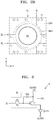
- FIG. 2A is a top-plan view showing a layout of pixels of the display panel 100 according to some example embodiments
- FIG. 2B is an excerpt top-plan view of a periphery of the first region R1 of the display panel 100 according to some example embodiments.
- a plurality of pixels may be arranged in display areas of the display panel 100, that is, the first display area DA1 and the second display area DA2.
- a plurality of first pixels P1 arranged in the first display area DA1 may each emit red, green, or blue light, and the first display area DA1 may provide or display a certain image by using the light emitted from the first pixels P1.
- Second pixels P2 arranged in the second display area DA2 may each emit red, green, or blue light, and the second display area DA2 may provide or display an image (e.g., a preset image) by using the light emitted from the second pixels P2.
- Each of the first regions R1 is a region in which pixels are not arranged, and the first pixels P1 may be arranged around the first region R1.
- the first pixels P1 are arranged along an edge of the first region R1, and two adjacent first pixels P1 may be arranged along the edge of the first region R1.
- the two adjacent pixels P1 may be apart from each other with the first region R1 therebetween.
- the first pixels P1 may each be electrically connected to a scanning line SL extending in the first direction (for example, the x direction) and a data line DL extending in the second direction (for example, the y direction).
- the scanning line SL and the data line DL respectively extending in the first direction and the second direction may detour around the first region R1.
- the scanning lines SL may each extend in the first direction and detour along or around the edge of the first region R1
- the data lines DL may each extend in the second direction and detour along or around the edge of the first region R1.
- a first detour area MA1 along which the scanning lines SL and/or the data lines DL detour may be arranged between the first region R1 and the first display area DA1.
- FIG. 3 is an equivalent circuit diagram of a pixel P included in the display panel 100 of the display apparatus 1 according to some example embodiments.
- the pixel P may include a pixel circuit PC and an organic light-emitting diode OLED as a display element connected to the pixel circuit PC.
- the pixel circuit PC may include a first thin-film transistor T1, a second thin-film transistor T2, and a storage capacitor Cst.
- Each pixel P may emit red, green, blue light or emit red, green, blue, or white light from the organic light-emitting diode OLED.
- the second thin-film transistor T2 which is a switching thin-film transistor, may be connected to the scanning line SL and the data line DL and may be configured to deliver a data voltage input from the data line DL to the first thin-film transistor T1, based on a switching voltage input from the scanning line SL.
- the storage capacitor Cst may be connected to the second thin-film transistor T2 and a driving voltage line PL and store a voltage corresponding to a difference between a voltage received from the second thin-film transistor T2 and a first power voltage ELVDD supplied to the driving voltage line PL.
- the first thin-film transistor T1 which is a driving thin-film transistor, may be connected to the driving voltage line PL and the storage capacitor Cst and control a driving current flowing from the driving voltage line PL to the organic light-emitting diode OLED to correspond to a value of the voltage stored in the storage capacitor Cst.
- the organic light-emitting diode OLED may emit light having a certain luminance according to the driving current.
- a common electrode (for example, a cathode) of the organic light-emitting diode OLED may receive a second power voltage ELVSS.
- the pixel circuit PC including two thin-film transistors and one storage capacitor is described with reference to FIG. 3 , according to some example embodiments, the number of thin-film transistors and the number of storage capacitors may be variously modified according to designs of the pixel circuit PC.
- the pixel circuit PC may further include one or more thin-film transistors in addition to the two thin-film transistors stated above.
- the pixel P described with reference to FIG. 3 may correspond to each of the first pixel P1 and the second pixel P2 described above with reference to FIGS. 2A and 2B .
- the first pixel P1 may include a first pixel circuit and a first organic light-emitting diode OLED1 connected thereto and the second pixel P2 may include a second pixel circuit and a second organic light-emitting diode OLED2 connected thereto.
- the first pixel circuit and the second pixel circuit may include a same number of thin-film transistors and storage capacitors. According to some example embodiments, the first pixel circuit and the second pixel circuit may include different numbers of thin-film transistors and storage capacitors. For example, the first pixel circuit may include two thin-film transistors and one storage capacitor and the second pixel circuit may further include one or more thin-film transistors in addition to two thin-film transistors.
- FIG. 4 is a schematic cross-sectional view of the display panel 100 according to some example embodiments.
- the display panel 100 includes a display layer DL1 arranged on a substrate 101.
- the substrate 101 may be flexible.
- the substrate 101 may include a polymer resin.
- the substrate 101 may include a polymer resin such as polyethersulfone, polyarylate, polyetherimide, polyethylene naphthalate, polyethylene terephthalate, polyphenylene sulfide, polyimide, polycarbonate (PC), cellulose triacetate (TAC), cellulose acetate propionate, and the like.
- a polymer resin such as polyethersulfone, polyarylate, polyetherimide, polyethylene naphthalate, polyethylene terephthalate, polyphenylene sulfide, polyimide, polycarbonate (PC), cellulose triacetate (TAC), cellulose acetate propionate, and the like.
- a barrier layer may be further included between the display layer DL1 and the substrate 101.
- the barrier layer which is a barrier layer for preventing or reducing permeation of external foreign materials or contaminants, may be a single layer or multi-layer including an inorganic material such as silicon nitride (SiN x , x>0) or silicon oxide (SiO x , x>0).
- the display layer DL1 may include a display element layer DEL, which includes a plurality of display elements, and a pixel circuit layer PCL including a pixel circuit and insulating layers.
- the display element layer DEL may include display elements, for example, first organic light-emitting diodes OLED1 and second organic light-emitting diodes OLED2 as described above.
- the pixel circuit layer PCL may include the pixel circuits and insulating layers respectively connected to the first organic light-emitting diodes OLED1 or the second organic light-emitting diodes OLED2.
- the pixel circuit layer PCL may include a plurality of transistors, storage capacitors, and insulating layers between the plurality of transistors and the storage capacitors.
- Display elements may be covered by an encapsulation member such as a thin-film encapsulation layer TFE.
- the thin-film encapsulation layer TFE may include at least one inorganic encapsulation layer and at least one organic encapsulation layer covering the display element layer DEL.
- the display panel 100 includes the substrate 101, which includes the polymer resin, and the thin-film encapsulation layer TFE including the inorganic encapsulation layer and the organic encapsulation layer. Accordingly, the display panel 100 may be a flexible display panel having flexibility.
- a touch electrode layer TSL including touch electrodes is arranged on the thin-film encapsulation layer TFE, and an optical functional layer OFL may be arranged on the touch electrode layer TSL.
- the touch electrode layer TSL may obtain coordinate information according to an external output, for example, a touch event.
- the optical functional layer OFL may reduce reflectivity of light (external light) incident from outside toward the display panel 100 and/or improve color purity of light emitted from the display panel 100.
- the optical functional layer OFL may include a retarder and a polarizer.
- the retarder may include a film-type or liquid crystal coating-type retarder and include a ⁇ /2 and/or a ⁇ /4 retarder.
- the polarizer may also include a film-type polarizer or a liquid crystal coating-type polarizer.
- a film-type polarizer may include a stretched-type synthetic resin film, and a liquid crystal coating-type polarizer may include liquid crystals arranged into a certain arrangement.
- the retarder and the polarizer may further include a protection film.
- the optical functional layer OFL may include a black matrix and color filters.
- the color filters may be arranged considering colors of light that is emitted from each pixel of the display panel 100.
- Each of the color filters may include a red, green, or blue pigment or dye.
- each of the color filters may further include quantum dots in addition to the pigment or dye stated above.
- some of the color filters may not include the pigment or dye stated above, and may include scattered particles such as titanium oxide.
- the optical functional layer OFL may include a destructive interference structure.
- the destructive interference structure may include a first reflective layer and a second reflective layer respectively arranged on different layers. First reflected light and second reflected light respectively reflected from the first reflective layer and the second reflective layer may undergo destructive interference, and accordingly, a reflectance of external light may be reduced.
- An adhesion member may be arranged between the touch electrode layer TSL and the optical functional layer OFL.
- General adhesion members known in the art may be non-limitedly adopted as the adhesion member.
- the adhesion member may be a pressure sensitive adhesive (PSA).
- the display panel 100 may include a first opening portion 1000A corresponding to a first region R1.
- a plurality of layers constructing the display panel 100 for example, the substrate 101, the display layer DL1, and the thin-film encapsulation layer TFE, may respectively include opening portions 101OA, PCLOA, and TFEOA corresponding to the first opening portion 100OA.
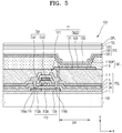
- FIG. 5 shows a cross-section corresponding to a portion of the first pixel P1 that is a portion of the display apparatus 1 according to some example embodiments.
- the pixel circuit layer PCL is arranged on the substrate 101.
- FIG. 5 shows that the pixel circuit layer PCL includes a thin-film transistor TFT and a buffer layer 111, a first gate insulating layer 113a, a second gate insulating layer 113b, an interlayer insulating layer 115, and a planarization insulating layer 117 arranged under and/or above components of the thin-film transistor TFT.
- the buffer layer 111 may include an inorganic material, such as silicon nitride, silicon oxynitride, and silicon oxide, and may include a single layer or multi-layer including the above-stated inorganic material.
- an inorganic material such as silicon nitride, silicon oxynitride, and silicon oxide
- the thin-film transistor TFT may include a semiconductor layer 112, and the semiconductor layer 112 may include polysilicon. Alternatively, the semiconductor layer 112 may include amorphous silicon, an oxide semiconductor, an organic semiconductor, or the like.
- the semiconductor layer 112 may include a channel area 112c and a drain area 112a and a source area 112b respectively arranged at two sides of the channel area 112c.
- a gate electrode 114 may overlap the channel area 112c.
- the gate electrode 114 may include a low-resistance metal material.
- the gate electrode 114 may include a conductive material including molybdenum (Mo), aluminum (Al), copper (Cu), titanium (Ti), and the like and include a multi-layer or single layer including the above-stated material.
- the first gate insulating layer 113a between the semiconductor layer 112 and the gate electrode 114 may include an inorganic insulating material such as silicon oxide (SiO 2 ), silicon nitride (SiN x ), silicon oxynitride (SiON), aluminum oxide (Al 2 O 3 ), titanium oxide (TiO 2 ), tantalum oxide (Ta 2 O 5 ), hafnium oxide (HfO 2 ), or zinc oxide (ZnO 2 ).
- silicon oxide SiO 2
- SiN x silicon nitride
- SiON silicon oxynitride
- Al 2 O 3 aluminum oxide
- TiO 2 titanium oxide
- Ta 2 O 5 tantalum oxide
- hafnium oxide HfO 2
- ZnO 2 zinc oxide
- the second gate insulating layer 113b may be provided to cover the gate electrode 114. Similar to the first gate insulating layer 113a, the second gate insulating layer 113b may include an inorganic insulating material such as SiO 2 , SiN x , SiON, Al 2 O 3 , TiO 2 , Ta 2 O 5 , HfO 2 , or ZnO 2 .
- an inorganic insulating material such as SiO 2 , SiN x , SiON, Al 2 O 3 , TiO 2 , Ta 2 O 5 , HfO 2 , or ZnO 2 .
- An upper electrode Cst2 of the storage capacitor Cst may be arranged on the second gate insulating layer 113b.
- the upper electrode Cst2 may overlap the gate electrode 114 under the upper electrode Cst2.
- the gate electrode 114 and the upper electrode Cst2 overlapping with the second gate insulating layer 113b therebetween may construct the storage capacitor Cst. That is, the gate electrode 114 may function as a lower electrode Cst1 of the storage capacitor Cst.
- the storage capacitor Cst and the thin-film transistor TFT may be formed to overlap each other. According to some example embodiments, the storage capacitor Cst may also be formed not to overlap the thin-film transistor TFT.
- the upper electrode Cst2 may include aluminum (Al), platinum (Pt), palladium (Pd), silver (Ag), magnesium (Mg), gold (Au), nickel (Ni), neodymium (Nd), iridium (Ir), chromium (Cr), calcium (Ca), molybdenum (Mo), titanium (Ti), tungsten (W), and/or copper (Cu) and include a single layer or multi-layer including the above-stated materials.
- the interlayer insulating layer 115 may cover the upper electrode Cst2.
- the interlayer insulating layer 115 may include silicon oxide (SiO 2 ), silicon nitride (SiN x ), silicon oxynitride (SiON), aluminum oxide (Al 2 O 3 ), titanium oxide (TiO 2 ), tantalum oxide (Ta 2 O 5 ), hafnium oxide (HfO 2 ), zinc oxide (ZnO 2 ), or the like.
- the interlayer insulating layer 115 may include a single layer or multi-layer including the above-stated inorganic insulating materials.
- a drain electrode 116a and a source electrode 116b may each be on the interlayer insulating layer 115.
- the drain electrode 116a and the source electrode 116b may include materials having excellent conductivity.
- the drain electrode 116a and the source electrode 116b may each include a conductive material including Mo, Al, Cu, Ti, and the like and include a multi-layer or single layer including the above-stated materials.
- the drain electrode 116a and the source electrode 116b may each have a multi-layer structure of Ti/Al/Ti.
- the planarization insulating layer 117 may include an organic insulating layer.
- the planarization insulating layer 117 may include an organic insulating material such as a general commercial polymer like polymethylmethacrylate (PMMA) or polystyrene (PS), a polymer derivative having a phenolic group, an acryl-based polymer, an imide-based polymer, an aryl ether-based polymer, an amide-based polymer, a fluoride-based polymer, a p-xylene based polymer, a vinyl alcohol-based polymer, and a blend thereof.
- PMMA polymethylmethacrylate
- PS polystyrene
- the display element layer DEL is arranged on the pixel circuit layer PCL of the above-described structure.
- the display element layer DEL may include the first organic light-emitting diode OLED1, and a pixel electrode 121 of the first organic light-emitting diode OLED1 may be electrically connected to the thin-film transistor TFT via a contact hole in the planarization insulating layer 117.
- the pixel electrode 121 may include a conductive oxide such as indium tin oxide (ITO), indium zinc oxide (IZO), zinc oxide (ZnO), indium oxide (In 2 O 3 ), indium gallium oxide (IGO), or aluminum zinc oxide (AZO).
- the pixel electrode 121 may include a reflective film including Ag, Mg, Al, Pt, Pd, Au, Ni, Nd, Ir, Cr, or a compound thereof.
- the pixel electrode 121 may include a film including ITO, IZO, ZnO, or In 2 O 3 above/under the above-stated reflective film.
- a pixel defining layer 119 having an opening 119OP that exposes a center portion of the pixel electrode 121 is arranged on the pixel electrode 121.
- the pixel defining layer 119 may include an organic insulating material and/or an inorganic insulating material.
- the opening 119OP may define an emission area (hereinafter, referred to as a first emission area EA1) of light emitted from the first organic light-emitting diode OLED1.
- a width of the opening 119OP may correspond to a width of the first emission area EA1.
- An emission layer 122 may be arranged in the opening 119OP of the pixel defining layer 119.
- the emission layer 122 may include a high molecular weight organic material or a low molecular weight organic material emitting light of a certain color.
- a first functional layer and a second functional layer may be arranged respectively under and above the emission layer 122.
- the first functional layer may include a hole transport layer (HTL) or include an HTL and a hole injection layer (HIL).
- HTL hole transport layer
- HIL hole injection layer
- the second functional layer is a component arranged on the emission layer 122 and may be omitted.
- the second functional layer may include an electron transport layer (ETL) and/or an electron injection layer (EIL).
- ETL electron transport layer
- EIL electron injection layer
- the first functional layer and/or the second functional layer may be common layers formed to entirely cover the substrate 101, like a common electrode 123 to be described hereinafter.
- the common electrode 123 may include a conductive material having a small work function.
- the common electrode 123 may include a (semi)transparent layer including Ag, Mg, Al, Pt, Pd, Au, Ni, Nd, Ir, Cr, Li, Ca, an alloy thereof, and the like.
- the common electrode 123 may further include a layer such as ITO, IZO, ZnO, or In 2 O 3 on the (semi)transparent layer including the above-stated materials.
- the thin-film encapsulation layer TFE includes at least one inorganic encapsulation layer and at least one organic encapsulation layer.
- FIG. 5 shows that the thin-film encapsulation layer TFE includes a first inorganic encapsulation layer 131, an organic encapsulation layer 132, and a second inorganic encapsulation layer 133 that are sequentially stacked.
- the first inorganic encapsulation layer 131 and the second inorganic encapsulation layer 133 may include one or more inorganic materials from among aluminum oxide, titanium oxide, tantalum oxide, hafnium oxide, zinc oxide, silicon oxide, silicon nitride, and silicon oxynitride.
- the organic encapsulation layer 132 may include a polymer-based material.
- the polymer-based material may include an acryl-based resin, an epoxy-based resin, polyimide, polyethylene, and the like. According to some example embodiments, the organic encapsulation layer 132 may include acrylate.
- the second pixel P2 as a portion of the display panel 100 may have a same structure as the first pixel P1 described above with reference to FIG. 5 .
- the second organic light-emitting diode OLED2 of the second pixel P2 may include a pixel electrode, an emission layer, and a common electrode.
- a second emission area of the second organic light-emitting diode OLED2 may be defined by an opening of a pixel defining layer that exposes the pixel electrode of the second organic light-emitting diode OLED2.
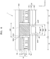
- FIG. 6 is a cross-sectional view of the first region R1 in the display apparatus 1 according to some example embodiments.
- reference numerals that are the same as those in FIGS. 4 and 5 indicate same members, some repeated descriptions thereof will be omitted.
- the display apparatus 1 may include the display panel 100, a cover window CW above the display panel 100, and a protective member 200 under the display panel 100.
- the display apparatus 1 may include a supporting member 300 to correspond to the first region R1.
- the display panel 100 may include the first opening portion 100OA as described above.
- the cover window CW may be a flexible window member.
- the cover window CW may be flexibly bent by an external force without cracks occurring and the like and protect the display panel 100.
- the cover window CW may include glass, sapphire, or plastic.
- the cover window CW may include ultra thin glass (UTG) or colorless polyimide (CPI).
- UTG ultra thin glass
- CPI colorless polyimide
- a general cover window known in the field may be non-limitedly used as the cover window CW.
- the cover window CW may have a structure in which a flexible polymer layer is arranged on a surface of a glass substrate or only include a polymer layer.
- the display apparatus 1 may further include a protective film above the cover window CW.
- the display apparatus 1 may include a protective member 200 under the display panel 100.
- the protective member 200 absorbs external impacts to prevent the organic light-emitting diode OLED and the like arranged on the display panel 100 from being damaged due to the external impacts.
- the protective member 200 attaches the display panel 100 without damaging other components such as a case 20.
- the protective member 200 may include a film layer 201, a cushion layer 203, and a metal plate 205.
- the film layer 201 may be arranged under the display panel 100.
- the film layer 201 may shield a region of the display panel except another region from which an image is output, such that the region is not seen by the user.
- the film layer 201 may block static electricity. That is, the film layer 201 may cover an area substantially corresponding to the first detour area MA1 shown in Fig. 2B .
- the cushion layer 203 and the metal plate 205 may cover the entire area of the display panel 100.
- the film layer 201 may include a film layer opening portion to correspond to the first opening portion 100OA.
- the film layer 201 may include the film layer opening portion to correspond to the first region R1.
- a planar size (e.g., a footprint when viewed from a plan view) of the film layer opening portion may be identical to a planar size (e.g., a footprint when viewed from a plan view) of the first opening portion 100OA.
- the film layer opening portion may be connected to the first opening portion 100OA.
- the film layer 201 may include at least one of carbon black, carbon nanotube, and CrO 2 .
- the film layer 201 may also include a material mixed with resin and the like, in addition to the above-stated materials.
- the film layer 201 may include a black tape.
- the film layer 201 may include a publicly known material that is capable of blocking light.
- the cushion layer 203 may be arranged under the film layer 201.
- the cushion layer 203 may protect the display panel 100 from external impacts.
- the cushion layer 203 may include a second opening portion 203OP.
- the second opening portion 203OP may be arranged to correspond to the first opening portion 100OA.
- the second opening portion 203OP may be arranged to correspond to the first region R1.
- a planar size of the second opening portion 203OP may be smaller than the planar size of the first opening portion 100OA.
- FIG. 6 shows that a width 203R of the second opening portion 203OP in a direction is less than a width 100R of the first opening portion 1000A in a direction.
- a portion of the cushion layer 203 adjacent to the second opening portion 203OP may be arranged in the first opening portion 100OA. That is, at least a portion of an upper surface of the cushion layer 203 may be arranged in the first opening portion 100OA. Accordingly, the supporting member 300 to be described in more detail later may be supported by the cushion layer 203.
- the cushion layer 203 may include polymer resin foam.
- the cushion layer 203 may include foam including polyurethane, polyethylene, polycarbonate, polypropylene, or polyolefin.
- the above-stated materials are only examples, and the cushion layer 203 may include a material that has excellent compressive stress and excellent absorption property for impact and vibration.
- the cushion layer 203 and the film layer 201 may be connected to each other by using a first adhesive member PSA1.
- the first adhesive member PSA1 may be omitted.
- the first adhesive member PSA1 may include an adhesive material such as a polyurethane-based material, a polyacryl-based material, a polyester-based material, a polyepoxy-based material, or a polyvinyl acetate-based material.
- the first adhesive member PSA1 is not limited thereto, and the first adhesive member PSA1 may include any suitable adhesive material for connecting the cushion layer 203 and the film layer 201.
- the metal plate 205 may be arranged under the cushion layer 203.
- the metal plate 205 may protect the display panel 100 from external heat, electromagnetic waves, and the like.
- the metal plate 205 may include a third opening portion 205OP.
- the third opening portion 205OP may be arranged to correspond to the second opening portion 203OP.
- the third opening portion 205OP and the second opening portion 203OP may be connected to each other.
- a planar size of the third opening portion 205OP may be smaller than or identical to the planar size of the second opening portion 203OP.
- a width of the third opening portion 205OP in a direction may be smaller than or identical to a width of the second opening portion 203OP in a direction. Accordingly, the metal plate 205 may stably support the cushion layer 203 that supports the supporting member 300.
- the metal plate 205 may include a high modulus material.
- the metal plate 205 may include at least one of invar, nobinite, stainless, and an alloy thereof. As the metal plate 205 may include a high modulus material, even when the display panel 100 is repeatedly bent, the metal plate 205 may not be deformed.
- the supporting member 300 may be arranged over the cushion layer 203.
- the supporting member 300 may be supported by the cushion layer 203.
- the supporting member 300 may be arranged to correspond to the first opening portion 100OA. Accordingly, the supporting member 300 may be arranged on the second opening portion 203OP and shield the second opening portion 203OP. In other words, the supporting member 300 may be arranged on an area of the cushion layer 203 that is adjacent to the second opening portion 203OP.
- the supporting member 300 may support the cover window CW.
- a lower portion of the supporting member 300 may be connected to the cushion layer 203 and an upper portion of the supporting member 300 may be connected to the cover window CW.
- the supporting member 300 may be connected to the cushion layer 203 through the first adhesive member PSA1.
- the supporting member 300 may also be connected to the cover window CW through a second adhesive member PSA2.
- the second adhesive member PSA2 is arranged on a whole lower surface of the cover window CW.
- the second adhesive member PSA2 may be separately arranged in a portion being attached to the display panel 100 and a portion being attached to the supporting member 300.
- a planar size of the supporting member 300 may be greater than the planar size of the second opening portion 203OP.
- a width 300R of the supporting member 300 in a direction may be greater than a width 203R of the second opening portion 203OP in said direction. Accordingly, the supporting member 300 may shield the second opening portion 203OP and may be connected to the cushion layer 203.
- the width 300R of the supporting member 300 in the direction may be smaller than the width 100R of the first opening portion 100OA in the direction. Accordingly, the supporting member 300 may be arranged in the first opening portion 1000A of the display panel 100.
- the planar size of the supporting member 300 may be greater than a planar size of the third opening portion 205OP.
- the width 300R of the supporting member 300 in the direction may be greater than a width of the third opening portion 205OP in a direction. Accordingly, the supporting member 300 may be supported by the cushion layer 203 and the cushion layer 203 may be stably supported by the metal plate 205.
- a thickness of the supporting member 300 may be identical to a thickness of the display panel 100. According to some example embodiments, a thickness of the supporting member 300 may be greater than a thickness of the display panel 100. Accordingly, the supporting member 300 may stably support the cover window CW.
- the supporting member 300 may include glass, sapphire, or a polymer resin. Alternatively, the supporting member 300 may include a high modulus material. In addition, the supporting member 300 may include a transparent material that may transmit sound or light from a component 400 to be described later. For example, the supporting member 300 may include a material having a transmittance from about 70 % to about 100 %. Accordingly, the supporting member 300 may stably support the cover window CW and prevent or reduce deformation of the cover window CW. In addition, the supporting member 300 may transmit light or sound from the component 400.
- the component 400 may be arranged to overlap the first region R1.
- the component 400 may be arranged under the display panel 100.
- the component 400 may be arranged in the second opening portion 203OP or the third opening portion 205OP.
- the component 400 may be arranged under the supporting member 300.
- the component 400 may be arranged under the third opening portion 205OP.
- the first region R1 may be understood as a location at which the component 400 is arranged, that is, a kind of component area (for example, a camera area, a sensor area, and the like).
- the component 400 may be arranged or spaced apart from the supporting member 300, such that there is a separation between the component 400 and the supporting member 300.
- the component 400 may be arranged or spaced apart from the supporting member 300 under the supporting member 300.
- the cushion layer 203 may shrink or compress. In this case, the component 400 may remain sufficiently separated from the supporting member 300 and may not undergo interference or come into contact with the supporting member 300.
- a planar size of the component 400 may be smaller than the planar size of the second opening portion 203OP.
- the planar size of the component 400 may be smaller than the planar size of the third opening portion 205OP.
- a width 400R of the component 400 in a direction may be smaller than the width 203R of the second opening portion 203OP in the direction.
- the width 400R of the component 400 in the direction may be smaller than a width of the third opening portion 205OP in the direction. Accordingly, the component 400 may be arranged in the second opening portion 203OP or the third opening portion 205OP.
- the component 400 may be an electronic element that may output and/or receive sound or light.
- the electronic element may include a sensor for outputting and/or receiving light, such as an infrared ray sensor, a camera for receiving light and capturing an image, a small-sized lamp for outputting light, a speaker for outputting sound, a microphone for receiving sound, and the like.
- the sensor may include a proximity sensor, a luminance sensor, a sensor for recognizing an iris, a sensor for recognizing a fingerprint, and the like.
- An electronic element using light may use light of various wavelength bands such as visible light, infrared light, ultraviolet light, and the like.
- the first region R1 may be a region through which sound or/and light proceeding to the outside from the component 400 or proceeding toward the component 400 from the outside may be transmitted.
- the sound or/and light emitted from the component 400 may proceed to the outside via the first region R1, and external light or/and sound from the outside may proceed toward the component 400 via the first region R1.
- the supporting member 300 may be arranged to prevent or reduce deformation of the cover window CW when the display apparatus 1 is folded.
- the cover window CW may be deformed.
- the cover window CW may be deformed in the first region R1.
- light or sound proceeding toward (i.e., received by) the component 400 may be distorted.
- the supporting member 300 may be arranged on the cushion layer 203. That is, even when the display apparatus 1 is repeatedly folded, the supporting member 300 that has a relatively high modulus may be arranged under the cover window CW and prevent or reduce deformation of the cover window CW. Accordingly, distortion of light or sound proceeding toward the component 400 arranged in the first region R1 may be prevented or reduced. In addition, according to some example embodiments, even when the cover window CW is repeatedly folded, crack of the cover window CW in the first region R1 may be prevented or reduced.
- External impacts may be delivered from the cover window CW to the supporting member 300.
- the cushion layer 203 may absorb the impacts.
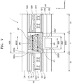
- FIG. 7 is a cross-sectional view of the first region R1 in a display apparatus 1' according to some example embodiments.
- reference numerals that are the same as those in FIG. 6 indicate same members, repeated descriptions thereof may be omitted.
- the display apparatus 1' may include the display panel 100, the cover window CW above the display panel 100, and the protective member 200 under the display panel 100.
- the display apparatus 1' may include a supporting member 300' to correspond to the first region R1.
- a size of an upper surface of the supporting member 300' may be smaller than a size of a lower surface of the supporting member 300'.
- a width 300UR of the upper surface of the supporting member 300' in a direction may be smaller than a width 300DR of the lower surface of the supporting member 300' in a direction.
- a width 301R in a direction of a plane including a first point 301 in the supporting member 300' may be greater than a width 302R in a direction of a plane a second point 302 in the supporting member 300'.
- the second point 302 may be closer to the cover window CW than the first point 301.
- the supporting member 300' in a planar view, may have a trapezoid shape. According to some example embodiments, it may be sufficient when the supporting member 300' has an upper surface having a smaller size than a lower surface thereof.
- a degree of deformation of an upper portion of the display panel 100 may be greater than a degree of deformation of a lower portion of the display panel 100. That is, the degree of deformation of the display panel 100 may increase from the substrate 101 of the display panel 100 toward the cover window CW.
- the supporting member 300 may be designed in consideration of the degree of deformation of the display panel 100 based on a thickness direction of the display panel 100. In other words, interference between the supporting member 300' and the display panel 100 may be prevented or reduced by having the width 300UR of the upper surface of the supporting member 300' in the direction smaller than the width 300DR of the lower surface of the supporting member 300' in the direction.
- FIG. 8A shows a simulation result of an embodiment.
- FIG. 8B shows a simulation result of a comparative example for comparison with the embodiment.
- the cover window may be deformed when a supporting member is arranged on a cushion layer, the supporting member is arranged so as to be connected to the cover window, and the display apparatus is repeatedly folded and unfolded.
- a maximum deformation value of the cover window was 0.48 um. The deformation is deformation of the cover window in a thickness direction.
- FIG. 8B shows a simulation result of deformation of the cover window when the display apparatus of the comparative example, in which the supporting member is not arranged, is repeatedly folded and unfolded.
- a maximum deformation value of the cover window is 6.6 um.
- the deformation is deformation of the cover window in a thickness direction.
- the supporting member when the supporting member is arranged on the cushion layer and the supporting member is arranged so as to be connected to the cover window, the deformation of the cover window may be prevented or reduced.
- the display apparatus according to some example embodiments have been described by using the term supporting member 300, but the embodiments are not limited thereto.
- the supporting member 300 may also be understood as the cover glass.
- a display apparatus having high reliability by preventing deformation of the cover window by arranging a supporting member in a transmission area in which a camera or the like is arranged, may be provided.
Landscapes
- Physics & Mathematics (AREA)
- Engineering & Computer Science (AREA)
- Microelectronics & Electronic Packaging (AREA)
- Nonlinear Science (AREA)
- General Physics & Mathematics (AREA)
- Signal Processing (AREA)
- Chemical & Material Sciences (AREA)
- Crystallography & Structural Chemistry (AREA)
- Mathematical Physics (AREA)
- Optics & Photonics (AREA)
- Geometry (AREA)
- Theoretical Computer Science (AREA)
- Electroluminescent Light Sources (AREA)
- Devices For Indicating Variable Information By Combining Individual Elements (AREA)
Abstract
Description
- Aspects of one or more embodiments relate to a display apparatus.
- Recently, display apparatuses have been used for various purposes. In addition, due to relatively small thicknesses and light weight, the range of potential uses for display apparatuses has expanded.
- As the potential uses for display apparatuses has expanded, various methods may be used for designing the form of display apparatuses, and functions that may be added or linked to the display apparatuses are increasing.
- In addition, as display apparatuses are more widely used, foldable display apparatuses may be more commonly utilized.
- The above information disclosed in this Background section is only for enhancement of understanding of the background and therefore the information discussed in this Background section does not necessarily constitute prior art.
- As a method increasing functions that may be added or linked to a display apparatus, one or more example embodiments include a display apparatus including areas, in which a camera, a sensor, and the like may be arranged in an inner side of a display area.
- One or more example embodiments include a foldable display apparatus having relatively high reliability.
- However, the above-described characteristics are merely examples of some characteristics of embodiments according to the present disclosure, and the scope of the embodiments according to the present disclosure is not limited thereto.
- Additional aspects will be set forth in part in the description which follows and, in part, will be more apparent from the description, or may be learned by practice of the presented example embodiments of the disclosure.
- According to some example embodiments, a display apparatus includes a display panel including a first opening portion and a display area at least partially surrounding the first opening portion, a cushion layer under the display panel and including a second opening portion, the second opening portion corresponding to the first opening portion and having a planar size smaller than a planar size of the first opening portion, a supporting member in the first opening portion above the cushion layer, and a cover window supported by the supporting member and arranged above the display panel.
- The display panel may include a display layer, wherein the display layer is not provided at the first opening portion.
- According to some example embodiments, a planar size of the supporting member may be greater than the planar size of the second opening portion.
- According to some example embodiments, the supporting member may be configured to shield the second opening portion.
- According to some example embodiments, a planar size of the supporting member may be greater than the planar size of the second opening portion and smaller than the planar size of the first opening portion.
- According to some example embodiments, the display apparatus may further include, under the cushion layer, a metal plate including a third opening corresponding to the second opening portion.
- According to some example embodiments, a planar size of the third opening portion may be smaller than or equal to the planar size of the second opening portion.
- According to some example embodiments, a planar size of the supporting member including a first point in the supporting member may be greater than a planar size of the supporting member including a second point, and the second point may be closer to the cover window than the first point is.
- According to some example embodiments, the supporting member may include glass or a polymer resin.
- According to some example embodiments, the display apparatus may further include a component under the supporting member.
- According to some example embodiments, the supporting member and the component may be spaced apart from each other.
- According to some example embodiments, a planar size of the component may be smaller than the planar size of the second opening portion.
- According to some example embodiments, a transmittance of the supporting member may be range from 70 % to 100 %.
- According to some example embodiments, the display panel may include a flexible display panel.
- Preferably, a thickness of the supporting member, i.e. a length in the z direction, may be identical to a thickness of the display panel or it may be greater than a thickness of the display panel.
- According to some example embodiments, a display apparatus includes a display panel including a first opening portion and a display area at least partially surrounding the first opening portion, a cover window above the display panel, a cover glass connected to the cover window and arranged in the first opening portion, and a cushion layer under the cover glass, wherein the cushion layer may include a second opening portion corresponding to the first opening portion, and a planar size of the first opening portion is greater than a planar size of the second opening portion.
- According to some example embodiments, the cover glass may be configured to shield the second opening portion.
- According to some example embodiments, the display apparatus may further include, under the cushion layer, a metal plate including a third opening portion corresponding to the second opening portion.
- According to some example embodiments, a size of the third opening portion may be smaller than or equal to a size of the second opening portion.
- According to some example embodiments, the display apparatus may further include a component under the cover glass.
- According to some example embodiments, a size of an upper surface of the cover glass may be smaller than a size of a lower surface of the cover glass.
- According to some example embodiments, the display panel may include a flexible display panel.
- Other aspects, features, and characteristics that are not described above will be more clearly understood from the accompanying drawings, claims, and detailed description.
- The above and other aspects, features, and characteristics of certain embodiments of the disclosure will be more apparent from the following description taken in conjunction with the accompanying drawings, in which:
-
FIG. 1A is a schematic perspective view of a display apparatus according to some example embodiments; -
FIG. 1B is a perspective view illustrating a state in which a display apparatus according to some example embodiments is folded in one direction; -
FIG. 1C is a perspective view illustrating a state in which a display apparatus according to some example embodiments is folded in an opposite direction to the direction ofFIG. 1B -
FIG. 2A is a top-plan view showing a layout of pixels in a display panel according to some example embodiments; -
FIG. 2B is an excerpt of a top-plan view of a periphery of a first region of a display panel according to some example embodiments; -
FIG. 3 is an equivalent circuit diagram of a pixel included in a display panel of a display apparatus according to some example embodiments; -
FIG. 4 is a schematic cross-sectional view of a display panel according to some example embodiments; -
FIG. 5 shows a cross-section corresponding to a portion of a first pixel that is a portion of a display panel according to some example embodiments; -
FIG. 6 is a cross-sectional view of a first region in a display apparatus according to some example embodiments; -
FIG. 7 is a cross-sectional view of a first region in a display apparatus according to some example embodiments; -
FIG. 8A shows a simulation result according to some example embodiments; and -
FIG. 8B shows a simulation result of a comparative example for comparison with an embodiment. - Reference will now be made in detail to aspects of some embodiments, examples of which are illustrated in the accompanying drawings, wherein like reference numerals refer to like elements throughout. In this regard, the present example embodiments may have different forms and should not be construed as being limited to the descriptions set forth herein. Accordingly, the example embodiments are merely described below, by referring to the figures, to explain aspects of the present description. As used herein, the term "and/or" includes any and all combinations of one or more of the associated listed items. Throughout the disclosure, the expression "at least one of a, b, or c" indicates only a, only b, only c, both a and b, both a and c, both b and c, all of a, b, c, or variations thereof.
- Reference will now be made in more detail to aspects of some embodiments, examples of which are illustrated in the accompanying drawings, wherein like reference numerals refer to like elements throughout, and some overlapping or repetitive description may be omitted.
- It will be understood that although terms such as "first," "second" may be used to describe various components, these components are not limited by these terms, and the terms are only used to distinguish one component from one another.
- As used herein, the singular forms "a," "an," and "the" are intended to include the plural forms as well, unless the context clearly indicates otherwise.
- It will be further understood that the terms "comprise" and/or "comprising" used herein specify the presence of stated features or components, but do not preclude the presence or addition of one or more other features or components.
- In the example embodiments, it will be understood that when a layer, an area, or a component is referred as being on another layer, area, or component, the layer, area, or component may be directly on the other layer, area, or component, or an intervening layer, area, or component may be present therebetween.
- Sizes of components in the drawings may be exaggerated or reduced for convenience of explanation. In other words, since sizes and thicknesses of components in the drawings are arbitrarily illustrated for convenience of explanation, the present disclosure is not limited thereto.
- In following example embodiments, when a layer, area, or component is connected to another layer, area, or component, the layer, area, or component may be directly connected to the other layer, area, or component, and may be indirectly connected to the other layer, area, or component with another layer, area, or component therebetween. For example, in the present specification, when a layer, area, or component is electrically connected to another layer, area, or component, the layer, area, or component may be electrically connected in a direct manner to the other layer, area, or component, and electrically connected in an indirect manner to the other layer, area, or component with another layer, area, or component therebetween.
-
FIG. 1A schematically shows adisplay apparatus 1 according to some example embodiments;FIG. 1B illustrates a state in which thedisplay apparatus 1 according to some example embodiments is folded in a direction; andFIG. 1C illustrates a state in which thedisplay apparatus 1 according to some example embodiments is folded in a direction opposite to the direction ofFIG. 1B . - Referring to
FIG. 1A , thedisplay apparatus 1 may include adisplay panel 100 and a housing or acase 20. - As an apparatus for displaying images, the
display apparatus 1 may include a portable mobile apparatus such as a hand-held game console, a multimedia apparatus, and an ultramicro personal computer (PC). Thedisplay apparatus 1 to be described hereinafter may include a liquid crystal display, an electrophoretic display, an organic light-emitting display, an inorganic light-emitting display, a field emission display, a surface-conduction electron-emitter display, a quantum dot display, a plasma display, a cathode ray display, and the like. Hereinafter, thedisplay apparatus 1 according to some example embodiments is described by taking an organic light-emitting display as an example, but the embodiments may be applied to various types of display apparatuses as described above. - The
display panel 100 may include a display area DA that may provide images and a first region R1 that is at least partially surrounded by the display area DA. According to some example embodiments, the first region R1 may be completely surrounded by the display area DA. According to some example embodiments, however, the first region R1 may be only partially surrounded by the display area DA. In addition, the first region R1 may include a transmission area. AlthoughFIG. 1A shows that the first region R1 is arranged as one region at an edge of thedisplay panel 100, according to some example embodiments, the first region R1 may be arranged in plurality at various locations on thedisplay panel 100. - The
case 20 may include afirst portion 21 and asecond portion 23 respectively supporting portions of thedisplay panel 100. Thecase 20 may be folded about a folding axis FAX between thefirst portion 21 and thesecond portion 23. According to some example embodiments, athird portion 25 between thefirst portion 21 and thesecond portion 23 may have a hinge structure. - Referring to
FIGS. 1A and1B , thedisplay panel 100 may be folded together with thecase 20, and portions of thedisplay panel 100 folded about the folding axis FAX traversing the display area DA may face each other. Hereinafter, for convenience of explanation, of the display area DA that is a screen area, portions arranged at the two opposing sides about the folding axis FAX are respectively referred to as a first display area DA1 and a second display area DA2. - The
display panel 100 and thecase 20 may be folded with reference to the folding axis FAX such that thefirst portion 21 and thesecond portion 23 face each other. For example, referring toFIG. 1C , thefirst portion 21 and thesecond portion 23 may be arranged to face each other. In other words, two portions of a rear surface of thedisplay apparatus 1 may be arranged to face each other. Accordingly, a certain image may be displayed on the first display area DA1 exposed in a direction and the second display area DA2 exposed toward another direction. - Although
FIGS. 1A through 1C show only one folding axis FAX, according to some example embodiments, thedisplay apparatus 1 may include a plurality of folding axes FAX. In addition, the folding axis FAX may also be arranged in a second direction that intersects with a first direction. For example, the folding axis FAX may be in parallel to the y direction. However, the folding axis FAX may also be in parallel to the x direction that intersects with the y direction. - Hereinafter, a state of the
display apparatus 1 before being folded will be described in more detail below. -
FIG. 2A is a top-plan view showing a layout of pixels of thedisplay panel 100 according to some example embodiments, andFIG. 2B is an excerpt top-plan view of a periphery of the first region R1 of thedisplay panel 100 according to some example embodiments. - Referring to
FIG. 2A , a plurality of pixels may be arranged in display areas of thedisplay panel 100, that is, the first display area DA1 and the second display area DA2. A plurality of first pixels P1 arranged in the first display area DA1 may each emit red, green, or blue light, and the first display area DA1 may provide or display a certain image by using the light emitted from the first pixels P1. Second pixels P2 arranged in the second display area DA2 may each emit red, green, or blue light, and the second display area DA2 may provide or display an image (e.g., a preset image) by using the light emitted from the second pixels P2. - Each of the first regions R1 is a region in which pixels are not arranged, and the first pixels P1 may be arranged around the first region R1. The first pixels P1 are arranged along an edge of the first region R1, and two adjacent first pixels P1 may be arranged along the edge of the first region R1. The two adjacent pixels P1 may be apart from each other with the first region R1 therebetween.
- The first pixels P1 may each be electrically connected to a scanning line SL extending in the first direction (for example, the x direction) and a data line DL extending in the second direction (for example, the y direction). The scanning line SL and the data line DL respectively extending in the first direction and the second direction may detour around the first region R1. As shown in
FIG. 2B , the scanning lines SL may each extend in the first direction and detour along or around the edge of the first region R1, and the data lines DL may each extend in the second direction and detour along or around the edge of the first region R1. - As described above, a first detour area MA1 along which the scanning lines SL and/or the data lines DL detour may be arranged between the first region R1 and the first display area DA1.
-
FIG. 3 is an equivalent circuit diagram of a pixel P included in thedisplay panel 100 of thedisplay apparatus 1 according to some example embodiments. - Referring to
FIG. 3 , the pixel P may include a pixel circuit PC and an organic light-emitting diode OLED as a display element connected to the pixel circuit PC. - The pixel circuit PC may include a first thin-film transistor T1, a second thin-film transistor T2, and a storage capacitor Cst. Each pixel P may emit red, green, blue light or emit red, green, blue, or white light from the organic light-emitting diode OLED.
- The second thin-film transistor T2, which is a switching thin-film transistor, may be connected to the scanning line SL and the data line DL and may be configured to deliver a data voltage input from the data line DL to the first thin-film transistor T1, based on a switching voltage input from the scanning line SL. The storage capacitor Cst may be connected to the second thin-film transistor T2 and a driving voltage line PL and store a voltage corresponding to a difference between a voltage received from the second thin-film transistor T2 and a first power voltage ELVDD supplied to the driving voltage line PL.
- The first thin-film transistor T1, which is a driving thin-film transistor, may be connected to the driving voltage line PL and the storage capacitor Cst and control a driving current flowing from the driving voltage line PL to the organic light-emitting diode OLED to correspond to a value of the voltage stored in the storage capacitor Cst. The organic light-emitting diode OLED may emit light having a certain luminance according to the driving current. A common electrode (for example, a cathode) of the organic light-emitting diode OLED may receive a second power voltage ELVSS.
- Although the pixel circuit PC including two thin-film transistors and one storage capacitor is described with reference to
FIG. 3 , according to some example embodiments, the number of thin-film transistors and the number of storage capacitors may be variously modified according to designs of the pixel circuit PC. For example, the pixel circuit PC may further include one or more thin-film transistors in addition to the two thin-film transistors stated above. - The pixel P described with reference to
FIG. 3 may correspond to each of the first pixel P1 and the second pixel P2 described above with reference toFIGS. 2A and2B . For example, the first pixel P1 may include a first pixel circuit and a first organic light-emitting diode OLED1 connected thereto and the second pixel P2 may include a second pixel circuit and a second organic light-emitting diode OLED2 connected thereto. - The first pixel circuit and the second pixel circuit may include a same number of thin-film transistors and storage capacitors. According to some example embodiments, the first pixel circuit and the second pixel circuit may include different numbers of thin-film transistors and storage capacitors. For example, the first pixel circuit may include two thin-film transistors and one storage capacitor and the second pixel circuit may further include one or more thin-film transistors in addition to two thin-film transistors.
-
FIG. 4 is a schematic cross-sectional view of thedisplay panel 100 according to some example embodiments. - Referring to
FIG. 4 , thedisplay panel 100 includes a display layer DL1 arranged on asubstrate 101. Thesubstrate 101 may be flexible. Thesubstrate 101 may include a polymer resin. - The
substrate 101 may include a polymer resin such as polyethersulfone, polyarylate, polyetherimide, polyethylene naphthalate, polyethylene terephthalate, polyphenylene sulfide, polyimide, polycarbonate (PC), cellulose triacetate (TAC), cellulose acetate propionate, and the like. - A barrier layer may be further included between the display layer DL1 and the
substrate 101. The barrier layer, which is a barrier layer for preventing or reducing permeation of external foreign materials or contaminants, may be a single layer or multi-layer including an inorganic material such as silicon nitride (SiNx, x>0) or silicon oxide (SiOx, x>0). - The display layer DL1 may include a display element layer DEL, which includes a plurality of display elements, and a pixel circuit layer PCL including a pixel circuit and insulating layers. The display element layer DEL may include display elements, for example, first organic light-emitting diodes OLED1 and second organic light-emitting diodes OLED2 as described above. The pixel circuit layer PCL may include the pixel circuits and insulating layers respectively connected to the first organic light-emitting diodes OLED1 or the second organic light-emitting diodes OLED2. The pixel circuit layer PCL may include a plurality of transistors, storage capacitors, and insulating layers between the plurality of transistors and the storage capacitors.
- Display elements may be covered by an encapsulation member such as a thin-film encapsulation layer TFE. The thin-film encapsulation layer TFE may include at least one inorganic encapsulation layer and at least one organic encapsulation layer covering the display element layer DEL. The
display panel 100 includes thesubstrate 101, which includes the polymer resin, and the thin-film encapsulation layer TFE including the inorganic encapsulation layer and the organic encapsulation layer. Accordingly, thedisplay panel 100 may be a flexible display panel having flexibility. - A touch electrode layer TSL including touch electrodes is arranged on the thin-film encapsulation layer TFE, and an optical functional layer OFL may be arranged on the touch electrode layer TSL. The touch electrode layer TSL may obtain coordinate information according to an external output, for example, a touch event. The optical functional layer OFL may reduce reflectivity of light (external light) incident from outside toward the
display panel 100 and/or improve color purity of light emitted from thedisplay panel 100. According to some example embodiments, the optical functional layer OFL may include a retarder and a polarizer. The retarder may include a film-type or liquid crystal coating-type retarder and include a λ/2 and/or a λ/4 retarder. The polarizer may also include a film-type polarizer or a liquid crystal coating-type polarizer. A film-type polarizer may include a stretched-type synthetic resin film, and a liquid crystal coating-type polarizer may include liquid crystals arranged into a certain arrangement. The retarder and the polarizer may further include a protection film. - As another example, the optical functional layer OFL may include a black matrix and color filters. The color filters may be arranged considering colors of light that is emitted from each pixel of the
display panel 100. Each of the color filters may include a red, green, or blue pigment or dye. Alternatively, each of the color filters may further include quantum dots in addition to the pigment or dye stated above. Alternatively, some of the color filters may not include the pigment or dye stated above, and may include scattered particles such as titanium oxide. - As another example, the optical functional layer OFL may include a destructive interference structure. The destructive interference structure may include a first reflective layer and a second reflective layer respectively arranged on different layers. First reflected light and second reflected light respectively reflected from the first reflective layer and the second reflective layer may undergo destructive interference, and accordingly, a reflectance of external light may be reduced.
- An adhesion member may be arranged between the touch electrode layer TSL and the optical functional layer OFL. General adhesion members known in the art may be non-limitedly adopted as the adhesion member. The adhesion member may be a pressure sensitive adhesive (PSA).
- The
display panel 100 may include afirst opening portion 1000A corresponding to a first region R1. A plurality of layers constructing thedisplay panel 100, for example, thesubstrate 101, the display layer DL1, and the thin-film encapsulation layer TFE, may respectively include opening portions 101OA, PCLOA, and TFEOA corresponding to the first opening portion 100OA. -
FIG. 5 shows a cross-section corresponding to a portion of the first pixel P1 that is a portion of thedisplay apparatus 1 according to some example embodiments. - The pixel circuit layer PCL is arranged on the
substrate 101.FIG. 5 shows that the pixel circuit layer PCL includes a thin-film transistor TFT and abuffer layer 111, a firstgate insulating layer 113a, a secondgate insulating layer 113b, aninterlayer insulating layer 115, and aplanarization insulating layer 117 arranged under and/or above components of the thin-film transistor TFT. - The
buffer layer 111 may include an inorganic material, such as silicon nitride, silicon oxynitride, and silicon oxide, and may include a single layer or multi-layer including the above-stated inorganic material. - The thin-film transistor TFT may include a
semiconductor layer 112, and thesemiconductor layer 112 may include polysilicon. Alternatively, thesemiconductor layer 112 may include amorphous silicon, an oxide semiconductor, an organic semiconductor, or the like. Thesemiconductor layer 112 may include achannel area 112c and adrain area 112a and asource area 112b respectively arranged at two sides of thechannel area 112c. Agate electrode 114 may overlap thechannel area 112c. - The
gate electrode 114 may include a low-resistance metal material. Thegate electrode 114 may include a conductive material including molybdenum (Mo), aluminum (Al), copper (Cu), titanium (Ti), and the like and include a multi-layer or single layer including the above-stated material. - The first
gate insulating layer 113a between thesemiconductor layer 112 and thegate electrode 114 may include an inorganic insulating material such as silicon oxide (SiO2), silicon nitride (SiNx), silicon oxynitride (SiON), aluminum oxide (Al2O3), titanium oxide (TiO2), tantalum oxide (Ta2O5), hafnium oxide (HfO2), or zinc oxide (ZnO2). - The second
gate insulating layer 113b may be provided to cover thegate electrode 114. Similar to the firstgate insulating layer 113a, the secondgate insulating layer 113b may include an inorganic insulating material such as SiO2, SiNx, SiON, Al2O3, TiO2, Ta2O5, HfO2, or ZnO2. - An upper electrode Cst2 of the storage capacitor Cst may be arranged on the second
gate insulating layer 113b. The upper electrode Cst2 may overlap thegate electrode 114 under the upper electrode Cst2. In this case, thegate electrode 114 and the upper electrode Cst2 overlapping with the secondgate insulating layer 113b therebetween may construct the storage capacitor Cst. That is, thegate electrode 114 may function as a lower electrode Cst1 of the storage capacitor Cst. - As described, the storage capacitor Cst and the thin-film transistor TFT may be formed to overlap each other. According to some example embodiments, the storage capacitor Cst may also be formed not to overlap the thin-film transistor TFT.
- The upper electrode Cst2 may include aluminum (Al), platinum (Pt), palladium (Pd), silver (Ag), magnesium (Mg), gold (Au), nickel (Ni), neodymium (Nd), iridium (Ir), chromium (Cr), calcium (Ca), molybdenum (Mo), titanium (Ti), tungsten (W), and/or copper (Cu) and include a single layer or multi-layer including the above-stated materials.
- The interlayer insulating
layer 115 may cover the upper electrode Cst2. The interlayer insulatinglayer 115 may include silicon oxide (SiO2), silicon nitride (SiNx), silicon oxynitride (SiON), aluminum oxide (Al2O3), titanium oxide (TiO2), tantalum oxide (Ta2O5), hafnium oxide (HfO2), zinc oxide (ZnO2), or the like. The interlayer insulatinglayer 115 may include a single layer or multi-layer including the above-stated inorganic insulating materials. - A
drain electrode 116a and asource electrode 116b may each be on theinterlayer insulating layer 115. Thedrain electrode 116a and thesource electrode 116b may include materials having excellent conductivity. Thedrain electrode 116a and thesource electrode 116b may each include a conductive material including Mo, Al, Cu, Ti, and the like and include a multi-layer or single layer including the above-stated materials. According to some example embodiments, thedrain electrode 116a and thesource electrode 116b may each have a multi-layer structure of Ti/Al/Ti. - The
planarization insulating layer 117 may include an organic insulating layer. Theplanarization insulating layer 117 may include an organic insulating material such as a general commercial polymer like polymethylmethacrylate (PMMA) or polystyrene (PS), a polymer derivative having a phenolic group, an acryl-based polymer, an imide-based polymer, an aryl ether-based polymer, an amide-based polymer, a fluoride-based polymer, a p-xylene based polymer, a vinyl alcohol-based polymer, and a blend thereof. - The display element layer DEL is arranged on the pixel circuit layer PCL of the above-described structure. The display element layer DEL may include the first organic light-emitting diode OLED1, and a
pixel electrode 121 of the first organic light-emitting diode OLED1 may be electrically connected to the thin-film transistor TFT via a contact hole in theplanarization insulating layer 117. - The
pixel electrode 121 may include a conductive oxide such as indium tin oxide (ITO), indium zinc oxide (IZO), zinc oxide (ZnO), indium oxide (In2O3), indium gallium oxide (IGO), or aluminum zinc oxide (AZO). According to some example embodiments, thepixel electrode 121 may include a reflective film including Ag, Mg, Al, Pt, Pd, Au, Ni, Nd, Ir, Cr, or a compound thereof. According to some example embodiments, thepixel electrode 121 may include a film including ITO, IZO, ZnO, or In2O3 above/under the above-stated reflective film. - A
pixel defining layer 119 having an opening 119OP that exposes a center portion of thepixel electrode 121 is arranged on thepixel electrode 121. Thepixel defining layer 119 may include an organic insulating material and/or an inorganic insulating material. The opening 119OP may define an emission area (hereinafter, referred to as a first emission area EA1) of light emitted from the first organic light-emitting diode OLED1. For example, a width of the opening 119OP may correspond to a width of the first emission area EA1. - An
emission layer 122 may be arranged in the opening 119OP of thepixel defining layer 119. Theemission layer 122 may include a high molecular weight organic material or a low molecular weight organic material emitting light of a certain color. According to some example embodiments, a first functional layer and a second functional layer may be arranged respectively under and above theemission layer 122. For example, the first functional layer may include a hole transport layer (HTL) or include an HTL and a hole injection layer (HIL). The second functional layer is a component arranged on theemission layer 122 and may be omitted. The second functional layer may include an electron transport layer (ETL) and/or an electron injection layer (EIL). The first functional layer and/or the second functional layer may be common layers formed to entirely cover thesubstrate 101, like acommon electrode 123 to be described hereinafter. - The
common electrode 123 may include a conductive material having a small work function. For example, thecommon electrode 123 may include a (semi)transparent layer including Ag, Mg, Al, Pt, Pd, Au, Ni, Nd, Ir, Cr, Li, Ca, an alloy thereof, and the like. Alternatively, thecommon electrode 123 may further include a layer such as ITO, IZO, ZnO, or In2O3 on the (semi)transparent layer including the above-stated materials. - The thin-film encapsulation layer TFE includes at least one inorganic encapsulation layer and at least one organic encapsulation layer. According to some example embodiments,
FIG. 5 shows that the thin-film encapsulation layer TFE includes a firstinorganic encapsulation layer 131, anorganic encapsulation layer 132, and a second inorganic encapsulation layer 133 that are sequentially stacked. - The first
inorganic encapsulation layer 131 and the second inorganic encapsulation layer 133 may include one or more inorganic materials from among aluminum oxide, titanium oxide, tantalum oxide, hafnium oxide, zinc oxide, silicon oxide, silicon nitride, and silicon oxynitride. Theorganic encapsulation layer 132 may include a polymer-based material. The polymer-based material may include an acryl-based resin, an epoxy-based resin, polyimide, polyethylene, and the like. According to some example embodiments, theorganic encapsulation layer 132 may include acrylate. - A cross-sectional structure corresponding to the first pixel P1 as a portion of the
display panel 100 has been described above with reference toFIG. 5 . However, according to some example embodiments, the second pixel P2 as a portion of thedisplay panel 100 may have a same structure as the first pixel P1 described above with reference toFIG. 5 . For example, the second organic light-emitting diode OLED2 of the second pixel P2 may include a pixel electrode, an emission layer, and a common electrode. As described above with reference toFIG. 5 , a second emission area of the second organic light-emitting diode OLED2 may be defined by an opening of a pixel defining layer that exposes the pixel electrode of the second organic light-emitting diode OLED2. -
FIG. 6 is a cross-sectional view of the first region R1 in thedisplay apparatus 1 according to some example embodiments. InFIG. 6 , as reference numerals that are the same as those inFIGS. 4 and5 indicate same members, some repeated descriptions thereof will be omitted. - The
display apparatus 1 may include thedisplay panel 100, a cover window CW above thedisplay panel 100, and aprotective member 200 under thedisplay panel 100. In addition, thedisplay apparatus 1 may include a supportingmember 300 to correspond to the first region R1. Thedisplay panel 100 may include the first opening portion 100OA as described above. - The cover window CW may be a flexible window member. The cover window CW may be flexibly bent by an external force without cracks occurring and the like and protect the
display panel 100. The cover window CW may include glass, sapphire, or plastic. For example, the cover window CW may include ultra thin glass (UTG) or colorless polyimide (CPI). A general cover window known in the field may be non-limitedly used as the cover window CW. For example, the cover window CW may have a structure in which a flexible polymer layer is arranged on a surface of a glass substrate or only include a polymer layer. Thedisplay apparatus 1 may further include a protective film above the cover window CW. - The
display apparatus 1 may include aprotective member 200 under thedisplay panel 100. Theprotective member 200 absorbs external impacts to prevent the organic light-emitting diode OLED and the like arranged on thedisplay panel 100 from being damaged due to the external impacts. In addition, theprotective member 200 attaches thedisplay panel 100 without damaging other components such as acase 20. - The
protective member 200 may include afilm layer 201, acushion layer 203, and ametal plate 205. - The
film layer 201 may be arranged under thedisplay panel 100. Thefilm layer 201 may shield a region of the display panel except another region from which an image is output, such that the region is not seen by the user. In addition, thefilm layer 201 may block static electricity. That is, thefilm layer 201 may cover an area substantially corresponding to the first detour area MA1 shown inFig. 2B . Thecushion layer 203 and themetal plate 205 may cover the entire area of thedisplay panel 100. - The
film layer 201 may include a film layer opening portion to correspond to the first opening portion 100OA. In other words, thefilm layer 201 may include the film layer opening portion to correspond to the first region R1. A planar size (e.g., a footprint when viewed from a plan view) of the film layer opening portion may be identical to a planar size (e.g., a footprint when viewed from a plan view) of the first opening portion 100OA. In addition, the film layer opening portion may be connected to the first opening portion 100OA. - The
film layer 201 may include at least one of carbon black, carbon nanotube, and CrO2. Thefilm layer 201 may also include a material mixed with resin and the like, in addition to the above-stated materials. Alternatively, thefilm layer 201 may include a black tape. Thefilm layer 201 may include a publicly known material that is capable of blocking light. - The
cushion layer 203 may be arranged under thefilm layer 201. Thecushion layer 203 may protect thedisplay panel 100 from external impacts. - The
cushion layer 203 may include a second opening portion 203OP. The second opening portion 203OP may be arranged to correspond to the first opening portion 100OA. In other words, the second opening portion 203OP may be arranged to correspond to the first region R1. - A planar size of the second opening portion 203OP may be smaller than the planar size of the first opening portion 100OA. Regarding this,
FIG. 6 shows that awidth 203R of the second opening portion 203OP in a direction is less than awidth 100R of thefirst opening portion 1000A in a direction. - Accordingly, a portion of the
cushion layer 203 adjacent to the second opening portion 203OP may be arranged in the first opening portion 100OA. That is, at least a portion of an upper surface of thecushion layer 203 may be arranged in the first opening portion 100OA. Accordingly, the supportingmember 300 to be described in more detail later may be supported by thecushion layer 203. - The
cushion layer 203 may include polymer resin foam. For example, thecushion layer 203 may include foam including polyurethane, polyethylene, polycarbonate, polypropylene, or polyolefin. However, the above-stated materials are only examples, and thecushion layer 203 may include a material that has excellent compressive stress and excellent absorption property for impact and vibration. - The
cushion layer 203 and thefilm layer 201 may be connected to each other by using a first adhesive member PSA1. When thecushion layer 203 includes an adhesive material, the first adhesive member PSA1 may be omitted. The first adhesive member PSA1 may include an adhesive material such as a polyurethane-based material, a polyacryl-based material, a polyester-based material, a polyepoxy-based material, or a polyvinyl acetate-based material. However, the first adhesive member PSA1 is not limited thereto, and the first adhesive member PSA1 may include any suitable adhesive material for connecting thecushion layer 203 and thefilm layer 201. - The
metal plate 205 may be arranged under thecushion layer 203. Themetal plate 205 may protect thedisplay panel 100 from external heat, electromagnetic waves, and the like. - The
metal plate 205 may include a third opening portion 205OP. The third opening portion 205OP may be arranged to correspond to the second opening portion 203OP. In addition, the third opening portion 205OP and the second opening portion 203OP may be connected to each other. - A planar size of the third opening portion 205OP may be smaller than or identical to the planar size of the second opening portion 203OP. For example, a width of the third opening portion 205OP in a direction may be smaller than or identical to a width of the second opening portion 203OP in a direction. Accordingly, the
metal plate 205 may stably support thecushion layer 203 that supports the supportingmember 300. - The
metal plate 205 may include a high modulus material. For example, themetal plate 205 may include at least one of invar, nobinite, stainless, and an alloy thereof. As themetal plate 205 may include a high modulus material, even when thedisplay panel 100 is repeatedly bent, themetal plate 205 may not be deformed. - The supporting
member 300 may be arranged over thecushion layer 203. For example, the supportingmember 300 may be supported by thecushion layer 203. - The supporting
member 300 may be arranged to correspond to the first opening portion 100OA. Accordingly, the supportingmember 300 may be arranged on the second opening portion 203OP and shield the second opening portion 203OP. In other words, the supportingmember 300 may be arranged on an area of thecushion layer 203 that is adjacent to the second opening portion 203OP. - The supporting
member 300 may support the cover window CW. For example, a lower portion of the supportingmember 300 may be connected to thecushion layer 203 and an upper portion of the supportingmember 300 may be connected to the cover window CW. The supportingmember 300 may be connected to thecushion layer 203 through the first adhesive member PSA1. In addition, the supportingmember 300 may also be connected to the cover window CW through a second adhesive member PSA2. Referring toFIG. 6 , the second adhesive member PSA2 is arranged on a whole lower surface of the cover window CW. However, according to some example embodiments, the second adhesive member PSA2 may be separately arranged in a portion being attached to thedisplay panel 100 and a portion being attached to the supportingmember 300. - A planar size of the supporting
member 300 may be greater than the planar size of the second opening portion 203OP. For example, awidth 300R of the supportingmember 300 in a direction may be greater than awidth 203R of the second opening portion 203OP in said direction. Accordingly, the supportingmember 300 may shield the second opening portion 203OP and may be connected to thecushion layer 203. Thewidth 300R of the supportingmember 300 in the direction may be smaller than thewidth 100R of the first opening portion 100OA in the direction. Accordingly, the supportingmember 300 may be arranged in thefirst opening portion 1000A of thedisplay panel 100. - The planar size of the supporting
member 300 may be greater than a planar size of the third opening portion 205OP. For example, thewidth 300R of the supportingmember 300 in the direction may be greater than a width of the third opening portion 205OP in a direction. Accordingly, the supportingmember 300 may be supported by thecushion layer 203 and thecushion layer 203 may be stably supported by themetal plate 205. - According to some example embodiments, a thickness of the supporting member 300 (for example, a length in the z direction) may be identical to a thickness of the
display panel 100. According to some example embodiments, a thickness of the supportingmember 300 may be greater than a thickness of thedisplay panel 100. Accordingly, the supportingmember 300 may stably support the cover window CW. - The supporting
member 300 may include glass, sapphire, or a polymer resin. Alternatively, the supportingmember 300 may include a high modulus material. In addition, the supportingmember 300 may include a transparent material that may transmit sound or light from acomponent 400 to be described later. For example, the supportingmember 300 may include a material having a transmittance from about 70 % to about 100 %. Accordingly, the supportingmember 300 may stably support the cover window CW and prevent or reduce deformation of the cover window CW. In addition, the supportingmember 300 may transmit light or sound from thecomponent 400. - The
component 400 may be arranged to overlap the first region R1. Thecomponent 400 may be arranged under thedisplay panel 100. For example, thecomponent 400 may be arranged in the second opening portion 203OP or the third opening portion 205OP. Accordingly, thecomponent 400 may be arranged under the supportingmember 300. However, according to some example embodiments, thecomponent 400 may be arranged under the third opening portion 205OP. The first region R1 may be understood as a location at which thecomponent 400 is arranged, that is, a kind of component area (for example, a camera area, a sensor area, and the like). - The
component 400 may be arranged or spaced apart from the supportingmember 300, such that there is a separation between thecomponent 400 and the supportingmember 300. For example, thecomponent 400 may be arranged or spaced apart from the supportingmember 300 under the supportingmember 300. When thedisplay apparatus 1 is folded, thecushion layer 203 may shrink or compress. In this case, thecomponent 400 may remain sufficiently separated from the supportingmember 300 and may not undergo interference or come into contact with the supportingmember 300. - A planar size of the
component 400 may be smaller than the planar size of the second opening portion 203OP. In addition, the planar size of thecomponent 400 may be smaller than the planar size of the third opening portion 205OP. For example, awidth 400R of thecomponent 400 in a direction may be smaller than thewidth 203R of the second opening portion 203OP in the direction. In addition, thewidth 400R of thecomponent 400 in the direction may be smaller than a width of the third opening portion 205OP in the direction. Accordingly, thecomponent 400 may be arranged in the second opening portion 203OP or the third opening portion 205OP. - The
component 400 may be an electronic element that may output and/or receive sound or light. For example, the electronic element may include a sensor for outputting and/or receiving light, such as an infrared ray sensor, a camera for receiving light and capturing an image, a small-sized lamp for outputting light, a speaker for outputting sound, a microphone for receiving sound, and the like. The sensor may include a proximity sensor, a luminance sensor, a sensor for recognizing an iris, a sensor for recognizing a fingerprint, and the like. An electronic element using light may use light of various wavelength bands such as visible light, infrared light, ultraviolet light, and the like. - The first region R1 may be a region through which sound or/and light proceeding to the outside from the
component 400 or proceeding toward thecomponent 400 from the outside may be transmitted. The sound or/and light emitted from thecomponent 400 may proceed to the outside via the first region R1, and external light or/and sound from the outside may proceed toward thecomponent 400 via the first region R1. - The supporting
member 300 may be arranged to prevent or reduce deformation of the cover window CW when thedisplay apparatus 1 is folded. When thedisplay apparatus 1 is afoldable display apparatus 1 and is repeatedly folded, the cover window CW may be deformed. For example, when the cover window CW is not supported by the supportingmember 300 in the first region R1, the cover window CW may be deformed in the first region R1. When the cover window CW in the first region R1 is deformed, light or sound proceeding toward (i.e., received by) thecomponent 400 may be distorted. - To minimize or reduce the above-stated phenomenon, according to some example embodiments, the supporting
member 300 may be arranged on thecushion layer 203. That is, even when thedisplay apparatus 1 is repeatedly folded, the supportingmember 300 that has a relatively high modulus may be arranged under the cover window CW and prevent or reduce deformation of the cover window CW. Accordingly, distortion of light or sound proceeding toward thecomponent 400 arranged in the first region R1 may be prevented or reduced. In addition, according to some example embodiments, even when the cover window CW is repeatedly folded, crack of the cover window CW in the first region R1 may be prevented or reduced. - External impacts may be delivered from the cover window CW to the supporting
member 300. However, according to some example embodiments, as the supportingmember 300 is arranged over thecushion layer 203, thecushion layer 203 may absorb the impacts. -
FIG. 7 is a cross-sectional view of the first region R1 in a display apparatus 1' according to some example embodiments. InFIG. 7 , as reference numerals that are the same as those inFIG. 6 indicate same members, repeated descriptions thereof may be omitted. - The display apparatus 1' may include the
display panel 100, the cover window CW above thedisplay panel 100, and theprotective member 200 under thedisplay panel 100. In addition, the display apparatus 1' may include a supporting member 300' to correspond to the first region R1. - A size of an upper surface of the supporting member 300' may be smaller than a size of a lower surface of the supporting member 300'. For example, a width 300UR of the upper surface of the supporting member 300' in a direction may be smaller than a width 300DR of the lower surface of the supporting member 300' in a direction. For example, a
width 301R in a direction of a plane including afirst point 301 in the supporting member 300' may be greater than awidth 302R in a direction of a plane asecond point 302 in the supporting member 300'. In this case, thesecond point 302 may be closer to the cover window CW than thefirst point 301. - According to some example embodiments, in a planar view, the supporting member 300' may have a trapezoid shape. According to some example embodiments, it may be sufficient when the supporting member 300' has an upper surface having a smaller size than a lower surface thereof.
- When the display apparatus 1' is folded, a degree of deformation of an upper portion of the
display panel 100 may be greater than a degree of deformation of a lower portion of thedisplay panel 100. That is, the degree of deformation of thedisplay panel 100 may increase from thesubstrate 101 of thedisplay panel 100 toward the cover window CW. - Accordingly, the supporting
member 300 may be designed in consideration of the degree of deformation of thedisplay panel 100 based on a thickness direction of thedisplay panel 100. In other words, interference between the supporting member 300' and thedisplay panel 100 may be prevented or reduced by having the width 300UR of the upper surface of the supporting member 300' in the direction smaller than the width 300DR of the lower surface of the supporting member 300' in the direction. -
FIG. 8A shows a simulation result of an embodiment.FIG. 8B shows a simulation result of a comparative example for comparison with the embodiment. - Referring to
FIG. 8A , the cover window may be deformed when a supporting member is arranged on a cushion layer, the supporting member is arranged so as to be connected to the cover window, and the display apparatus is repeatedly folded and unfolded. As a simulation result according to some example embodiments, a maximum deformation value of the cover window was 0.48 um. The deformation is deformation of the cover window in a thickness direction. -
FIG. 8B shows a simulation result of deformation of the cover window when the display apparatus of the comparative example, in which the supporting member is not arranged, is repeatedly folded and unfolded. In the comparative example, a maximum deformation value of the cover window is 6.6 um. The deformation is deformation of the cover window in a thickness direction. - Accordingly, when the supporting member is arranged on the cushion layer and the supporting member is arranged so as to be connected to the cover window, the deformation of the cover window may be prevented or reduced.
- The display apparatus according to some example embodiments have been described by using the
term supporting member 300, but the embodiments are not limited thereto. For example, the supportingmember 300 may also be understood as the cover glass. - As described above, according to some example embodiments, a display apparatus having high reliability by preventing deformation of the cover window by arranging a supporting member in a transmission area in which a camera or the like is arranged, may be provided.
- It should be understood that embodiments described herein should be considered in a descriptive sense only and not for purposes of limitation. Descriptions of features or aspects within each embodiment should typically be considered as available for other similar features or aspects in other embodiments. While one or more example embodiments have been described with reference to the figures, it will be understood by those of ordinary skill in the art that various changes in form and details may be made therein without departing from the scope as defined by the following claims.
Claims (15)
- A display apparatus (1,1') comprising:a display panel (100) comprising a first opening portion (100OA) and a display area (DA) at least partially surrounding the first opening portion (100OA);a cushion layer (203) under the display panel (100) and comprising a second opening portion (203OP), the second opening portion (203OP) overlapping the first opening portion (100OA) and having a planar size smaller than a planar size of the first opening portion (100OA);a supporting member (300, 300') in the first opening portion (203OP) above the cushion layer (203); anda cover window (CW) supported by the supporting member (300, 300') and arranged above the display panel (100).
- The display apparatus of claim 1, wherein a planar size of the supporting member (300, 300') is greater than the planar size of the second opening portion (203OP).
- The display apparatus of claim 2, wherein the supporting member (300, 300') is configured to shield the second opening portion (203OP).
- The display apparatus of claim 2, wherein a planar size of the supporting member (300, 300') is smaller than the planar size of the first opening portion (100OA).
- The display apparatus of one of the preceding claims, further comprising, under the cushion layer (203), a metal plate (205) comprising a third opening portion (205OP) overlapping the second opening portion (203OP).
- The display apparatus of claim 5, wherein a planar size of the third opening portion (205OP) is smaller than or equal to a planar size of the second opening portion (203OP).
- The display apparatus of claim 1, wherein a planar size of the supporting member (300') in a plane parallel to the surface of the cover window (CW) and comprising a first point (301) in the supporting member (300') is greater than a planar size of the supporting member (300') in a plane comprising a second point (302), wherein the second point (302) is closer to the cover window (CW) than the first point (301).
- The display apparatus of one of the preceding claims, wherein the supporting member (300, 300') comprises glass or a polymer resin.
- The display apparatus of one of the preceding claims, further comprising a component (400) under the supporting member (300, 300').
- The display apparatus of claim 9, wherein the supporting member (300, 300') and the component (400) are spaced apart from each other.
- The display apparatus of claim 9 or 10, wherein a planar size of the component (400) is smaller than a planar size of the second opening portion (203OP).
- The display apparatus of one of the preceding claims, wherein a transmittance of the supporting member (300, 300') ranges from 70 % to 100 %.
- The display apparatus of one of the preceding claims, wherein the display panel includes a flexible display panel.
- The display apparatus of one of the preceding claims,
wherein the supporting member (300, 300') is a cover glass connected to the cover window (CW). - The display apparatus of claim 14, wherein a size of an upper surface of the cover glass is smaller than a size of a lower surface of the cover glass.
Applications Claiming Priority (1)
| Application Number | Priority Date | Filing Date | Title |
|---|---|---|---|
| KR1020190108461A KR20210027718A (en) | 2019-09-02 | 2019-09-02 | Display apparatus |
Publications (2)
| Publication Number | Publication Date |
|---|---|
| EP3786694A1 true EP3786694A1 (en) | 2021-03-03 |
| EP3786694B1 EP3786694B1 (en) | 2023-05-03 |
Family
ID=72322357
Family Applications (1)
| Application Number | Title | Priority Date | Filing Date |
|---|---|---|---|
| EP20193843.8A Active EP3786694B1 (en) | 2019-09-02 | 2020-09-01 | Display apparatus |
Country Status (4)
| Country | Link |
|---|---|
| US (1) | US11160175B2 (en) |
| EP (1) | EP3786694B1 (en) |
| KR (1) | KR20210027718A (en) |
| CN (1) | CN112447808A (en) |
Families Citing this family (7)
| Publication number | Priority date | Publication date | Assignee | Title |
|---|---|---|---|---|
| US12165560B2 (en) * | 2019-11-18 | 2024-12-10 | Boe Technology Group Co., Ltd. | Display panel and display device |
| KR20220021081A (en) * | 2020-08-12 | 2022-02-22 | 삼성디스플레이 주식회사 | Display panel and display apparatus including the same |
| CN113296326A (en) * | 2021-05-20 | 2021-08-24 | 江西沃格光电股份有限公司 | Flexible electrochromic device and manufacturing method thereof |
| KR20230099218A (en) | 2021-12-27 | 2023-07-04 | 엘지디스플레이 주식회사 | Display apparatus |
| KR20230102841A (en) | 2021-12-30 | 2023-07-07 | 엘지디스플레이 주식회사 | Display apparatus and method of fabricating the same |
| KR20230139933A (en) | 2022-03-28 | 2023-10-06 | 삼성디스플레이 주식회사 | Display device |
| CN119152769A (en) * | 2023-06-14 | 2024-12-17 | 华为技术有限公司 | Screen and electronic device |
Citations (5)
| Publication number | Priority date | Publication date | Assignee | Title |
|---|---|---|---|---|
| US20160176151A1 (en) * | 2011-11-30 | 2016-06-23 | Samsung Display Co., Ltd. | Cushion sheet and display device having the same |
| CN107229148A (en) * | 2017-05-05 | 2017-10-03 | 广东欧珀移动通信有限公司 | Display screen, display device and mobile terminal |
| CN109120753A (en) * | 2018-08-21 | 2019-01-01 | 武汉天马微电子有限公司 | A display panel and display device |
| CN208401902U (en) * | 2018-04-26 | 2019-01-18 | Oppo广东移动通信有限公司 | terminal display screen component and mobile terminal |
| US20190245958A1 (en) * | 2018-02-05 | 2019-08-08 | Guangdong Oppo Mobile Telecommunications Corp., Ltd. | Terminal display assembly and mobile terminal |
Family Cites Families (12)
| Publication number | Priority date | Publication date | Assignee | Title |
|---|---|---|---|---|
| KR101406129B1 (en) | 2012-03-28 | 2014-06-13 | 엘지디스플레이 주식회사 | Display apparatus |
| US20160011633A1 (en) | 2013-03-15 | 2016-01-14 | Sharp Kabushiki Kaisha | Electronic device |
| KR20170111827A (en) | 2016-03-29 | 2017-10-12 | 삼성전자주식회사 | Electronic device including display and camera |
| KR102401285B1 (en) | 2016-04-01 | 2022-05-24 | 삼성전자주식회사 | Electronic device comprising display |
| KR102539196B1 (en) * | 2016-08-18 | 2023-06-02 | 삼성디스플레이 주식회사 | Flexible display device |
| KR102587736B1 (en) | 2016-09-02 | 2023-10-12 | 삼성전자주식회사 | Hidden Camera Module, Electronic Apparatus Being Applied Hidden Camera Module and the Managing Method thereof |
| KR102356866B1 (en) | 2017-04-10 | 2022-02-03 | 삼성디스플레이 주식회사 | Foldable display device and method for manufacturing the same |
| JP2018194632A (en) * | 2017-05-16 | 2018-12-06 | 株式会社ジャパンディスプレイ | Display device and display device manufacturing method |
| KR102295557B1 (en) * | 2017-09-15 | 2021-08-27 | 엘지디스플레이 주식회사 | Display device |
| JP2019095507A (en) * | 2017-11-20 | 2019-06-20 | 株式会社ジャパンディスプレイ | Display device |
| KR102522591B1 (en) * | 2018-02-05 | 2023-04-17 | 삼성디스플레이 주식회사 | Display device and manufacturing method thereof |
| US10991774B2 (en) * | 2018-02-12 | 2021-04-27 | Samsung Display Co., Ltd. | Display device and method for fabricating the same |
-
2019
- 2019-09-02 KR KR1020190108461A patent/KR20210027718A/en active Pending
-
2020
- 2020-04-14 US US16/848,570 patent/US11160175B2/en active Active
- 2020-08-27 CN CN202010877224.6A patent/CN112447808A/en active Pending
- 2020-09-01 EP EP20193843.8A patent/EP3786694B1/en active Active
Patent Citations (5)
| Publication number | Priority date | Publication date | Assignee | Title |
|---|---|---|---|---|
| US20160176151A1 (en) * | 2011-11-30 | 2016-06-23 | Samsung Display Co., Ltd. | Cushion sheet and display device having the same |
| CN107229148A (en) * | 2017-05-05 | 2017-10-03 | 广东欧珀移动通信有限公司 | Display screen, display device and mobile terminal |
| US20190245958A1 (en) * | 2018-02-05 | 2019-08-08 | Guangdong Oppo Mobile Telecommunications Corp., Ltd. | Terminal display assembly and mobile terminal |
| CN208401902U (en) * | 2018-04-26 | 2019-01-18 | Oppo广东移动通信有限公司 | terminal display screen component and mobile terminal |
| CN109120753A (en) * | 2018-08-21 | 2019-01-01 | 武汉天马微电子有限公司 | A display panel and display device |
Also Published As
| Publication number | Publication date |
|---|---|
| KR20210027718A (en) | 2021-03-11 |
| EP3786694B1 (en) | 2023-05-03 |
| US20210068274A1 (en) | 2021-03-04 |
| US11160175B2 (en) | 2021-10-26 |
| CN112447808A (en) | 2021-03-05 |
Similar Documents
| Publication | Publication Date | Title |
|---|---|---|
| EP3786694B1 (en) | Display apparatus | |
| US11404512B2 (en) | Display apparatus including auxiliary pixels | |
| US11289684B2 (en) | Display device and electronic apparatus | |
| US20230171990A1 (en) | Display apparatus | |
| US11038003B2 (en) | Foldable display apparatus | |
| US12185591B2 (en) | Display device with improved reliability and method of manufacturing the display device | |
| US12310175B2 (en) | Display panel and display device having center and adjacent corner areas spaced apart from each other by a penetration area | |
| KR102885846B1 (en) | Display Apparatus | |
| US12274153B2 (en) | Apparatus and method for manufacturing display device | |
| US20250048876A1 (en) | Display panel and display apparatus | |
| US11825708B2 (en) | Display panel and display device including first and second wirings | |
| US12364145B2 (en) | Display device and method of manufacturing display device | |
| KR20220014365A (en) | Display Device | |
| KR20230060634A (en) | Display Device | |
| US20240179974A1 (en) | Bending area structure of display apparatus and method of providing the same | |
| US20230134423A1 (en) | Display panel and display apparatus | |
| US20220208031A1 (en) | Display panel and display device | |
| US20240152184A1 (en) | Display apparatus, method of manufacturing the display apparatus, and electronic apparatus | |
| US20240042656A1 (en) | Apparatus and method for manufacturing display apparatus | |
| US12177998B2 (en) | Display apparatus and method of manufacturing display apparatus | |
| US20240172549A1 (en) | Display device | |
| US12610622B2 (en) | Display apparatus and method of manufacturing the display apparatus | |
| KR102903985B1 (en) | Display panel and display device | |
| US20230292583A1 (en) | Display panel and display device | |
| US20230380231A1 (en) | Display apparatus |
Legal Events
| Date | Code | Title | Description |
|---|---|---|---|
| PUAI | Public reference made under article 153(3) epc to a published international application that has entered the european phase |
Free format text: ORIGINAL CODE: 0009012 |
|
| STAA | Information on the status of an ep patent application or granted ep patent |
Free format text: STATUS: THE APPLICATION HAS BEEN PUBLISHED |
|
| AK | Designated contracting states |
Kind code of ref document: A1 Designated state(s): AL AT BE BG CH CY CZ DE DK EE ES FI FR GB GR HR HU IE IS IT LI LT LU LV MC MK MT NL NO PL PT RO RS SE SI SK SM TR |
|
| AX | Request for extension of the european patent |
Extension state: BA ME |
|
| STAA | Information on the status of an ep patent application or granted ep patent |
Free format text: STATUS: REQUEST FOR EXAMINATION WAS MADE |
|
| 17P | Request for examination filed |
Effective date: 20210608 |
|
| RBV | Designated contracting states (corrected) |
Designated state(s): AL AT BE BG CH CY CZ DE DK EE ES FI FR GB GR HR HU IE IS IT LI LT LU LV MC MK MT NL NO PL PT RO RS SE SI SK SM TR |
|
| GRAP | Despatch of communication of intention to grant a patent |
Free format text: ORIGINAL CODE: EPIDOSNIGR1 |
|
| STAA | Information on the status of an ep patent application or granted ep patent |
Free format text: STATUS: GRANT OF PATENT IS INTENDED |
|
| RIC1 | Information provided on ipc code assigned before grant |
Ipc: G02F 1/133 20060101ALN20220429BHEP Ipc: H04M 1/02 20060101ALI20220429BHEP Ipc: G02F 1/1333 20060101AFI20220429BHEP |
|
| INTG | Intention to grant announced |
Effective date: 20220602 |
|
| GRAJ | Information related to disapproval of communication of intention to grant by the applicant or resumption of examination proceedings by the epo deleted |
Free format text: ORIGINAL CODE: EPIDOSDIGR1 |
|
| STAA | Information on the status of an ep patent application or granted ep patent |
Free format text: STATUS: REQUEST FOR EXAMINATION WAS MADE |
|
| INTC | Intention to grant announced (deleted) | ||
| RIC1 | Information provided on ipc code assigned before grant |
Ipc: G02F 1/133 20060101ALN20221010BHEP Ipc: H04M 1/02 20060101ALI20221010BHEP Ipc: G02F 1/1333 20060101AFI20221010BHEP |
|
| GRAP | Despatch of communication of intention to grant a patent |
Free format text: ORIGINAL CODE: EPIDOSNIGR1 |
|
| STAA | Information on the status of an ep patent application or granted ep patent |
Free format text: STATUS: GRANT OF PATENT IS INTENDED |
|
| INTG | Intention to grant announced |
Effective date: 20221123 |
|
| GRAS | Grant fee paid |
Free format text: ORIGINAL CODE: EPIDOSNIGR3 |
|
| GRAA | (expected) grant |
Free format text: ORIGINAL CODE: 0009210 |
|
| STAA | Information on the status of an ep patent application or granted ep patent |
Free format text: STATUS: THE PATENT HAS BEEN GRANTED |
|
| AK | Designated contracting states |
Kind code of ref document: B1 Designated state(s): AL AT BE BG CH CY CZ DE DK EE ES FI FR GB GR HR HU IE IS IT LI LT LU LV MC MK MT NL NO PL PT RO RS SE SI SK SM TR |
|
| REG | Reference to a national code |
Ref country code: GB Ref legal event code: FG4D |
|
| REG | Reference to a national code |
Ref country code: DE Ref legal event code: R096 Ref document number: 602020010329 Country of ref document: DE |
|
| REG | Reference to a national code |
Ref country code: AT Ref legal event code: REF Ref document number: 1565131 Country of ref document: AT Kind code of ref document: T Effective date: 20230515 Ref country code: CH Ref legal event code: EP |
|
| REG | Reference to a national code |
Ref country code: IE Ref legal event code: FG4D |
|
| P01 | Opt-out of the competence of the unified patent court (upc) registered |
Effective date: 20230516 |
|
| REG | Reference to a national code |
Ref country code: LT Ref legal event code: MG9D |
|
| REG | Reference to a national code |
Ref country code: NL Ref legal event code: MP Effective date: 20230503 |
|
| REG | Reference to a national code |
Ref country code: AT Ref legal event code: MK05 Ref document number: 1565131 Country of ref document: AT Kind code of ref document: T Effective date: 20230503 |
|
| PG25 | Lapsed in a contracting state [announced via postgrant information from national office to epo] |
Ref country code: SE Free format text: LAPSE BECAUSE OF FAILURE TO SUBMIT A TRANSLATION OF THE DESCRIPTION OR TO PAY THE FEE WITHIN THE PRESCRIBED TIME-LIMIT Effective date: 20230503 Ref country code: PT Free format text: LAPSE BECAUSE OF FAILURE TO SUBMIT A TRANSLATION OF THE DESCRIPTION OR TO PAY THE FEE WITHIN THE PRESCRIBED TIME-LIMIT Effective date: 20230904 Ref country code: NO Free format text: LAPSE BECAUSE OF FAILURE TO SUBMIT A TRANSLATION OF THE DESCRIPTION OR TO PAY THE FEE WITHIN THE PRESCRIBED TIME-LIMIT Effective date: 20230803 Ref country code: NL Free format text: LAPSE BECAUSE OF FAILURE TO SUBMIT A TRANSLATION OF THE DESCRIPTION OR TO PAY THE FEE WITHIN THE PRESCRIBED TIME-LIMIT Effective date: 20230503 Ref country code: ES Free format text: LAPSE BECAUSE OF FAILURE TO SUBMIT A TRANSLATION OF THE DESCRIPTION OR TO PAY THE FEE WITHIN THE PRESCRIBED TIME-LIMIT Effective date: 20230503 Ref country code: AT Free format text: LAPSE BECAUSE OF FAILURE TO SUBMIT A TRANSLATION OF THE DESCRIPTION OR TO PAY THE FEE WITHIN THE PRESCRIBED TIME-LIMIT Effective date: 20230503 |
|
| PG25 | Lapsed in a contracting state [announced via postgrant information from national office to epo] |
Ref country code: RS Free format text: LAPSE BECAUSE OF FAILURE TO SUBMIT A TRANSLATION OF THE DESCRIPTION OR TO PAY THE FEE WITHIN THE PRESCRIBED TIME-LIMIT Effective date: 20230503 Ref country code: PL Free format text: LAPSE BECAUSE OF FAILURE TO SUBMIT A TRANSLATION OF THE DESCRIPTION OR TO PAY THE FEE WITHIN THE PRESCRIBED TIME-LIMIT Effective date: 20230503 Ref country code: LV Free format text: LAPSE BECAUSE OF FAILURE TO SUBMIT A TRANSLATION OF THE DESCRIPTION OR TO PAY THE FEE WITHIN THE PRESCRIBED TIME-LIMIT Effective date: 20230503 Ref country code: LT Free format text: LAPSE BECAUSE OF FAILURE TO SUBMIT A TRANSLATION OF THE DESCRIPTION OR TO PAY THE FEE WITHIN THE PRESCRIBED TIME-LIMIT Effective date: 20230503 Ref country code: IS Free format text: LAPSE BECAUSE OF FAILURE TO SUBMIT A TRANSLATION OF THE DESCRIPTION OR TO PAY THE FEE WITHIN THE PRESCRIBED TIME-LIMIT Effective date: 20230903 Ref country code: HR Free format text: LAPSE BECAUSE OF FAILURE TO SUBMIT A TRANSLATION OF THE DESCRIPTION OR TO PAY THE FEE WITHIN THE PRESCRIBED TIME-LIMIT Effective date: 20230503 Ref country code: GR Free format text: LAPSE BECAUSE OF FAILURE TO SUBMIT A TRANSLATION OF THE DESCRIPTION OR TO PAY THE FEE WITHIN THE PRESCRIBED TIME-LIMIT Effective date: 20230804 |
|
| PG25 | Lapsed in a contracting state [announced via postgrant information from national office to epo] |
Ref country code: FI Free format text: LAPSE BECAUSE OF FAILURE TO SUBMIT A TRANSLATION OF THE DESCRIPTION OR TO PAY THE FEE WITHIN THE PRESCRIBED TIME-LIMIT Effective date: 20230503 |
|
| PG25 | Lapsed in a contracting state [announced via postgrant information from national office to epo] |
Ref country code: SK Free format text: LAPSE BECAUSE OF FAILURE TO SUBMIT A TRANSLATION OF THE DESCRIPTION OR TO PAY THE FEE WITHIN THE PRESCRIBED TIME-LIMIT Effective date: 20230503 |
|
| PG25 | Lapsed in a contracting state [announced via postgrant information from national office to epo] |
Ref country code: SM Free format text: LAPSE BECAUSE OF FAILURE TO SUBMIT A TRANSLATION OF THE DESCRIPTION OR TO PAY THE FEE WITHIN THE PRESCRIBED TIME-LIMIT Effective date: 20230503 Ref country code: SK Free format text: LAPSE BECAUSE OF FAILURE TO SUBMIT A TRANSLATION OF THE DESCRIPTION OR TO PAY THE FEE WITHIN THE PRESCRIBED TIME-LIMIT Effective date: 20230503 Ref country code: RO Free format text: LAPSE BECAUSE OF FAILURE TO SUBMIT A TRANSLATION OF THE DESCRIPTION OR TO PAY THE FEE WITHIN THE PRESCRIBED TIME-LIMIT Effective date: 20230503 Ref country code: EE Free format text: LAPSE BECAUSE OF FAILURE TO SUBMIT A TRANSLATION OF THE DESCRIPTION OR TO PAY THE FEE WITHIN THE PRESCRIBED TIME-LIMIT Effective date: 20230503 Ref country code: DK Free format text: LAPSE BECAUSE OF FAILURE TO SUBMIT A TRANSLATION OF THE DESCRIPTION OR TO PAY THE FEE WITHIN THE PRESCRIBED TIME-LIMIT Effective date: 20230503 Ref country code: CZ Free format text: LAPSE BECAUSE OF FAILURE TO SUBMIT A TRANSLATION OF THE DESCRIPTION OR TO PAY THE FEE WITHIN THE PRESCRIBED TIME-LIMIT Effective date: 20230503 |
|
| REG | Reference to a national code |
Ref country code: DE Ref legal event code: R097 Ref document number: 602020010329 Country of ref document: DE |
|
| PLBE | No opposition filed within time limit |
Free format text: ORIGINAL CODE: 0009261 |
|
| STAA | Information on the status of an ep patent application or granted ep patent |
Free format text: STATUS: NO OPPOSITION FILED WITHIN TIME LIMIT |
|
| 26N | No opposition filed |
Effective date: 20240206 |
|
| REG | Reference to a national code |
Ref country code: CH Ref legal event code: PL |
|
| PG25 | Lapsed in a contracting state [announced via postgrant information from national office to epo] |
Ref country code: SI Free format text: LAPSE BECAUSE OF FAILURE TO SUBMIT A TRANSLATION OF THE DESCRIPTION OR TO PAY THE FEE WITHIN THE PRESCRIBED TIME-LIMIT Effective date: 20230503 |
|
| PG25 | Lapsed in a contracting state [announced via postgrant information from national office to epo] |
Ref country code: LU Free format text: LAPSE BECAUSE OF NON-PAYMENT OF DUE FEES Effective date: 20230901 |
|
| REG | Reference to a national code |
Ref country code: BE Ref legal event code: MM Effective date: 20230930 |
|
| PG25 | Lapsed in a contracting state [announced via postgrant information from national office to epo] |
Ref country code: SI Free format text: LAPSE BECAUSE OF FAILURE TO SUBMIT A TRANSLATION OF THE DESCRIPTION OR TO PAY THE FEE WITHIN THE PRESCRIBED TIME-LIMIT Effective date: 20230503 Ref country code: LU Free format text: LAPSE BECAUSE OF NON-PAYMENT OF DUE FEES Effective date: 20230901 Ref country code: IT Free format text: LAPSE BECAUSE OF FAILURE TO SUBMIT A TRANSLATION OF THE DESCRIPTION OR TO PAY THE FEE WITHIN THE PRESCRIBED TIME-LIMIT Effective date: 20230503 Ref country code: MC Free format text: LAPSE BECAUSE OF FAILURE TO SUBMIT A TRANSLATION OF THE DESCRIPTION OR TO PAY THE FEE WITHIN THE PRESCRIBED TIME-LIMIT Effective date: 20230503 |
|
| REG | Reference to a national code |
Ref country code: IE Ref legal event code: MM4A |
|
| PG25 | Lapsed in a contracting state [announced via postgrant information from national office to epo] |
Ref country code: IE Free format text: LAPSE BECAUSE OF NON-PAYMENT OF DUE FEES Effective date: 20230901 |
|
| PG25 | Lapsed in a contracting state [announced via postgrant information from national office to epo] |
Ref country code: CH Free format text: LAPSE BECAUSE OF NON-PAYMENT OF DUE FEES Effective date: 20230930 |
|
| PG25 | Lapsed in a contracting state [announced via postgrant information from national office to epo] |
Ref country code: IE Free format text: LAPSE BECAUSE OF NON-PAYMENT OF DUE FEES Effective date: 20230901 Ref country code: CH Free format text: LAPSE BECAUSE OF NON-PAYMENT OF DUE FEES Effective date: 20230930 |
|
| PG25 | Lapsed in a contracting state [announced via postgrant information from national office to epo] |
Ref country code: BE Free format text: LAPSE BECAUSE OF NON-PAYMENT OF DUE FEES Effective date: 20230930 |
|
| PG25 | Lapsed in a contracting state [announced via postgrant information from national office to epo] |
Ref country code: BG Free format text: LAPSE BECAUSE OF FAILURE TO SUBMIT A TRANSLATION OF THE DESCRIPTION OR TO PAY THE FEE WITHIN THE PRESCRIBED TIME-LIMIT Effective date: 20230503 |
|
| PG25 | Lapsed in a contracting state [announced via postgrant information from national office to epo] |
Ref country code: BG Free format text: LAPSE BECAUSE OF FAILURE TO SUBMIT A TRANSLATION OF THE DESCRIPTION OR TO PAY THE FEE WITHIN THE PRESCRIBED TIME-LIMIT Effective date: 20230503 |
|
| PG25 | Lapsed in a contracting state [announced via postgrant information from national office to epo] |
Ref country code: CY Free format text: LAPSE BECAUSE OF FAILURE TO SUBMIT A TRANSLATION OF THE DESCRIPTION OR TO PAY THE FEE WITHIN THE PRESCRIBED TIME-LIMIT; INVALID AB INITIO Effective date: 20200901 |
|
| PG25 | Lapsed in a contracting state [announced via postgrant information from national office to epo] |
Ref country code: HU Free format text: LAPSE BECAUSE OF FAILURE TO SUBMIT A TRANSLATION OF THE DESCRIPTION OR TO PAY THE FEE WITHIN THE PRESCRIBED TIME-LIMIT; INVALID AB INITIO Effective date: 20200901 |
|
| PGFP | Annual fee paid to national office [announced via postgrant information from national office to epo] |
Ref country code: DE Payment date: 20250820 Year of fee payment: 6 |
|
| PGFP | Annual fee paid to national office [announced via postgrant information from national office to epo] |
Ref country code: GB Payment date: 20250820 Year of fee payment: 6 |
|
| PGFP | Annual fee paid to national office [announced via postgrant information from national office to epo] |
Ref country code: FR Payment date: 20250821 Year of fee payment: 6 |
|
| PG25 | Lapsed in a contracting state [announced via postgrant information from national office to epo] |
Ref country code: TR Free format text: LAPSE BECAUSE OF FAILURE TO SUBMIT A TRANSLATION OF THE DESCRIPTION OR TO PAY THE FEE WITHIN THE PRESCRIBED TIME-LIMIT Effective date: 20230503 |