EP3786689A1 - Method and device for endless phase shifting of an optical signal - Google Patents
Method and device for endless phase shifting of an optical signal Download PDFInfo
- Publication number
- EP3786689A1 EP3786689A1 EP19194610.2A EP19194610A EP3786689A1 EP 3786689 A1 EP3786689 A1 EP 3786689A1 EP 19194610 A EP19194610 A EP 19194610A EP 3786689 A1 EP3786689 A1 EP 3786689A1
- Authority
- EP
- European Patent Office
- Prior art keywords
- optical
- phase
- phase shift
- stage
- signal
- Prior art date
- Legal status (The legal status is an assumption and is not a legal conclusion. Google has not performed a legal analysis and makes no representation as to the accuracy of the status listed.)
- Granted
Links
Images

Classifications
-
- G—PHYSICS
- G02—OPTICS
- G02F—OPTICAL DEVICES OR ARRANGEMENTS FOR THE CONTROL OF LIGHT BY MODIFICATION OF THE OPTICAL PROPERTIES OF THE MEDIA OF THE ELEMENTS INVOLVED THEREIN; NON-LINEAR OPTICS; FREQUENCY-CHANGING OF LIGHT; OPTICAL LOGIC ELEMENTS; OPTICAL ANALOGUE/DIGITAL CONVERTERS
- G02F1/00—Devices or arrangements for the control of the intensity, colour, phase, polarisation or direction of light arriving from an independent light source, e.g. switching, gating or modulating; Non-linear optics
- G02F1/01—Devices or arrangements for the control of the intensity, colour, phase, polarisation or direction of light arriving from an independent light source, e.g. switching, gating or modulating; Non-linear optics for the control of the intensity, phase, polarisation or colour
-
- H—ELECTRICITY
- H04—ELECTRIC COMMUNICATION TECHNIQUE
- H04B—TRANSMISSION
- H04B10/00—Transmission systems employing electromagnetic waves other than radio-waves, e.g. infrared, visible or ultraviolet light, or employing corpuscular radiation, e.g. quantum communication
- H04B10/60—Receivers
- H04B10/61—Coherent receivers
- H04B10/616—Details of the electronic signal processing in coherent optical receivers
- H04B10/6165—Estimation of the phase of the received optical signal, phase error estimation or phase error correction
-
- G—PHYSICS
- G02—OPTICS
- G02B—OPTICAL ELEMENTS, SYSTEMS OR APPARATUS
- G02B6/00—Light guides; Structural details of arrangements comprising light guides and other optical elements, e.g. couplings
- G02B6/24—Coupling light guides
- G02B6/26—Optical coupling means
- G02B6/28—Optical coupling means having data bus means, i.e. plural waveguides interconnected and providing an inherently bidirectional system by mixing and splitting signals
- G02B6/293—Optical coupling means having data bus means, i.e. plural waveguides interconnected and providing an inherently bidirectional system by mixing and splitting signals with wavelength selective means
- G02B6/29346—Optical coupling means having data bus means, i.e. plural waveguides interconnected and providing an inherently bidirectional system by mixing and splitting signals with wavelength selective means operating by wave or beam interference
- G02B6/2935—Mach-Zehnder configuration, i.e. comprising separate splitting and combining means
-
- G—PHYSICS
- G02—OPTICS
- G02F—OPTICAL DEVICES OR ARRANGEMENTS FOR THE CONTROL OF LIGHT BY MODIFICATION OF THE OPTICAL PROPERTIES OF THE MEDIA OF THE ELEMENTS INVOLVED THEREIN; NON-LINEAR OPTICS; FREQUENCY-CHANGING OF LIGHT; OPTICAL LOGIC ELEMENTS; OPTICAL ANALOGUE/DIGITAL CONVERTERS
- G02F1/00—Devices or arrangements for the control of the intensity, colour, phase, polarisation or direction of light arriving from an independent light source, e.g. switching, gating or modulating; Non-linear optics
- G02F1/01—Devices or arrangements for the control of the intensity, colour, phase, polarisation or direction of light arriving from an independent light source, e.g. switching, gating or modulating; Non-linear optics for the control of the intensity, phase, polarisation or colour
- G02F1/21—Devices or arrangements for the control of the intensity, colour, phase, polarisation or direction of light arriving from an independent light source, e.g. switching, gating or modulating; Non-linear optics for the control of the intensity, phase, polarisation or colour by interference
- G02F1/212—Mach-Zehnder type
Definitions
- the invention relates to an optical endless phase shifting device configured to shift an optical input signal by a desired phase shift as well as to a method therefore.
- phase-shifting of an optical signal occurs in connection with various communication components, especially in connection with coherent detection.
- coherent detection the data signal received is superimposed with a local oscillator signal, for instance in an optical 3-dB coupler, and the combined signal is received on a photodiode.
- coherent detection reveals an improved sensitivity for the detection of intensity-modulated optical signals.
- a drawback of coherent detection is the fact that the output electrical signal is also dependent on the phase difference between the optical signal to be received and the local oscillator signal with a sinusoidal function. If both even slightly differ in frequency, the electrical signal fades in and out with the combined frequency.
- a phase diversity receiver e.g. based on an optical hybrid.
- the drawback is the increased componentry, as the phase-diverse signals need to be received on multiple photodiodes and processed in parallel. It is therefore beneficial to directly control the phase of the local oscillator to match the phase of the data signal at the interference coupler (or have a fixed phase difference of ⁇ /2). This requires an optical phase shifter that can continuously rotate the phase of the local oscillator, even over many multiples of ⁇ , without the need to "reset" the phase, e.g. when the desired phase shift reaches a value equal to 2 ⁇ or an integer multiple thereof.
- a further application of an endless phase shifter is the stabilization of the phase of a laser. Supported by a PLL, comparing phase samples at different times, the endless phase shifter can be used to maintain a constant optical phase at the phase shifter output.
- a phase modulator can create a phase shift between 0 and 4pi.
- a waveguide parallel to the phase modulator has a fixed phase delay of 2 ⁇ .
- Optical switches before and after the structure allow to switch the signal between the phase modulator and the parallel waveguide.
- the modulator is at 0 or 4 ⁇ phase shift, the signal is switched to the parallel waveguide and the phase modulator is reset to a phase shift of 2 ⁇ .
- the optical switches before and after the phase modulator is a challenging task.
- the main drawbacks of this method and device for endless shifting an optical signal are that the phase modulator must provide a large phase shift range of 4 ⁇ and that fast switches and a fast modulator phase reset are required.
- An alternative endless phase shifter can be realized by an IQ-modulator structure, wherein in-phase and quadrature components are modulated, maintaining a constant amplitude and introducing a phase rotation. While this setup can continuously modulate the phase without fast switching or a fast phase reset, the intrinsic insertion loss is 6 dB, which in many cases cannot be tolerated.
- the optical endless phase shifting device comprises a first and a second stage.
- the first stage comprises a Mach-Zehnder structure comprising a passive optical splitter device configured to receive, at an input port, an optical input signal (E in ) and to split the input signal into a first and a second partial signal, each of which is fed, from a dedicated output port of the splitter device, to a first and a second branch of the first stage that connects the respected output port of the splitter device to a dedicated input port of a passive optical combiner device, the combiner device being configured to output a first combined signal at a first output port and a second combined signal at a second output port, each of the first and second branches of the first stage comprising a controllable optical phase shifter, wherein the phase shifter in the first branch is configured to shift the phase of the first partial signal by a positive predetermined phase shift and wherein the phase shifter in the second branch is configured to shift the phase of the second partial signal by a negative predetermined phase shift.
- the first stage realizes a Mach-Zehnder interferometer with push-pull configuration using an optical 2x2-coupler for creating two optical signals that are fed to the second stage.
- the second stage comprises a passive optical combiner device having a first input port connecting a first branch of the second stage to the first output port of the first stage combiner device and a second input port connecting a second branch of the second stage to the second output port of the first stage combiner device, the first branch or the first and second branches of the second stage comprising a controllable optical phase shifter, the combiner device being configured to output, at at least one output port, an optical output signal, which corresponds to the optical input signal that is phase-shifted by the desired phase shift.
- the optical phase shifters in the first branch or the first and second branches of the second stage are configured to be switchable between a first value of zero and a second value of ⁇ for a phase shift created by the respective optical phase shifter.
- the optical phase shifters in the first or the first and the second branches are switched, in order to provide the endless phase-shifting capability of the device, in a status in which the optical power of the signal in the respective branch is essentially zero. This mitigates the requirement of providing high-speed and high-precision switching.
- the first stage optical phase shifters are controllable in such a way that that they create a predetermined phase shift having an absolute value within a range from 0 to ⁇ /2 in case an optical phase shifter is provided in both branches of the second stage, or that they create a predetermined phase shift having an absolute value within a range from 0 to ⁇ in case an optical phase shifter is provided in only the first branch of the second stage.
- the phase-shift range of the phase shifters of the first stage can be restricted to a small range from zero to ⁇ /2.
- the endless-shifting capability of the device is achieved by switching the two phase shifters of the second stage into an appropriate status of zero or ⁇ , respectively, when, depending on the desired (total) phase shift, the absolute value of predetermined phase shift that is to be realized by each of the two phase shifters of the first stage reaches the upper or lower boundary of the phase shift range from zero to ⁇ /2.
- the neighboring status of the two switches of the second stage requires switching of only one of the phase shifters from zero to ⁇ or from ⁇ to zero, wherein the optical power of the signal present in the branch in which the phase shifter to be switched is provided is zero.
- the optical signal is proportional to the sine of the (positive) phase shift (or phase angle) created by phase shifters comprised in the branches of the first stage.
- these embodiments require a larger phase shift range for the predetermined phase shift from zero to ⁇ .
- the optical splitter device that is comprised by the first stage may be configured to output a first and a second optical output signal, wherein the electrical fields of the first and second optical output signals have essentially the same absolute value, but are shifted by ⁇ /2.
- optical 1x2 coupler e.g. an optical 1x2 fiber coupler or an optical integrated 1x2 coupler.
- the electrical field of the optical signal that is coupled from a pass-through path to the further output path is rotated by ⁇ /2.
- the optical combiner devices of the first and or second stage may be configured to create the first combined signal (E sin ) by adding the electrical field of the optical signal that is fed to the first input port and the electrical field of the optical signal that is fed to the second input port shifted by ⁇ /2, and the second combined signal (E cos ) by adding the electrical field of the optical signal that is fed to the second input port and the electrical field of the optical signal that is fed to the first input port shifted by ⁇ /2.
- Such an optical combiner device may be realized as an optical 1x2 coupler, e.g. an optical 1x2 fiber coupler or an optical integrated 1x2 coupler.
- E in , E sin and E cos designate complex field amplitudes of the optical input signal (E in ), the first combined signal and the second combined signal, respectively, and ⁇ designates the predetermined phase shift.
- This can be achieved by using an optical 1x2-coupler as a splitter device and an optical 2x2-coupler as a combiner device in the first stage.
- the endless phase shifting device may comprise a control device configured to receive a phase shift signal including the desired phase shift and to output control signals that are fed to the phase shifters of the first stage as well as one or two control signals that are fed to the one or two phase shifters of the second stage.
- a phase shifter is provided in both branches of the second stage and the at least one optical output signal is created according to the above alternative 1.
- the control device can be configured to create the control signals in such a way
- a phase shifter is provided in both branches of the second stage and the at least one optical output signal is created according to the above alternative 2.
- the control device can be configured create to the control signals in such a way
- control device in further embodiments, in which a phase shifter is provided in the first branch of the second stage only and the at least one optical output signal is created according to the above alternative 1, can be configured to create the control signals in such a way that the optical phase shifter of the second stage creates a phase shift zero if the desired phase shift is within a range from zero to ⁇ plus a positive integer times 2 ⁇ , and that the optical phase shifter of the second stage creates a phase shift ⁇ if the desired phase shift is within a range from ⁇ to 2 ⁇ plus a positive integer times 2 ⁇ .
- the control device can be configured to create the control signals in such a way that the optical phase shifter of the second stage creates a phase shift ⁇ if the desired phase shift is within a range from zero to ⁇ plus a positive integer times 2 ⁇ , and that the optical phase shifter of the second stage creates a phase shift zero if the desired phase shift is within a range from ⁇ to 2 ⁇ plus a positive integer times 2 ⁇ .
- the method for endless shifting of an optical input signal by a desired phase shift comprises the steps of:
- the method for endless shifting of an optical input signal by a desired phase shift comprises the steps of:
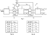
- Fig. 1 shows a schematic block diagram of a first embodiment of an optical endless phase shifting device 100 comprising a first stage 102 and a second stage 104. Both stages are controlled by a control device 106.
- the first stage comprises a Mach-Zehnder interferometer structure that is operated in push-pull configuration and that comprises a passive 1x2 optical splitter device 108, two controllable optical phase shifters 110, 112 and a passive 2x2 optical combiner device 114.
- the two controllable optical phase shifters 110, 112 are provided in a first and second branch of the first stage, wherein the first branch extends between a first splitting port of the passive optical splitter device 108 and a first input port of the passive optical combiner device 114, and the second branch extends between a second splitting port of the passive optical splitter device 108 and a second input port of the passive optical combiner device 114.
- the passive 1x2 optical splitter device 108 may be realized as a passive optical 1x2 fiber coupler or any other type of passive optical 1x2 coupler, e.g. an integrated waveguide coupler.
- the passive 2x2 optical combiner device 114 may be realized as a passive optical 2x2 fiber coupler or any other type of passive optical 2x2 coupler, e.g. an integrated waveguide coupler.
- Each of the two controllable phase shifters which may be realized in any arbitrary way, is configured to create a predetermined phase shift between an optical input signal received at an input port and an optical output signal output at an output port depending on a control signal S + ⁇ , S - ⁇ , e.g. a voltage, that is fed to a respective control port.
- the phase shifters 110, 112 are configured and controlled, by the control device 106, in such a way that a positive predetermined phase shift + ⁇ is created by the phase shifter 110 and a negative predetermined phase shift - ⁇ is created by the phase shifter 112.
- the phase shifters 110, 112 and the control device 106 are configured to create a positive and negative phase shift with an absolute value of ⁇ in the range of [0; ⁇ /2] depending on the respective control signal S + ⁇ , S - ⁇ that is supplied to the corresponding optical phase shifter device 110, 112 by the control device 106.
- the absolute value of the predetermined phase shift - ⁇ , + ⁇ is also referred to as differential phase shift.
- the second stage comprises a further passive optical 2x2 combiner device 116 and two further controllable optical phase shifters 118, 120.
- the two further controllable optical phase shifters 118, 120 are provided in a first and second branch of the second stage, wherein the first branch extends between a first output port of the passive optical combiner device 114 of the first stage and a first input port of the passive optical combiner device 116, and the second branch extends between a second output port of the passive optical combiner device 114 of the first stage and a second input port of the passive optical combiner device 116.
- Each of the phase shifters 118, 120 is configured to create an additional phase shift ⁇ 2, ⁇ 3 of zero or ⁇ between an input signal received at an input port and an output signal output at an output port, depending on a respective control signal S ⁇ 2 , S ⁇ 3 that is created by the control device 106.
- the whole optical endless phase shifting device 100 may be realized as a photonic integrated circuit (PIC).
- PIC photonic integrated circuit
- An optical input signal S in e.g. the optical signal created by a local oscillator of a coherent optical receiver, which is characterized by a complex amplitude E in , is fed to an input port of the passive optical splitter device 108.
- the endless phase shifting device 100 creates at least one optical output signal S out,1 , S out,2 , which is output at a respective output port of the passive optical combiner device 116 of the second stage 104, wherein the at least one output signal S out,1 , S out,2 corresponds to the optical input signal S in but is phase-shifted by a predetermined total phase shift ⁇ tot .
- the total phase shift ⁇ tot is also referred to as "desired phase shift".
- the passive optical 1x2 splitter device 108 which is preferably a 3dB splitter device, splits the input signal S in into two signals that are phase-shifted between each other by ⁇ /2 due to an inherent property of the passive optical splitter device 108. These signals are then shifted, by the respective optical phase shifter 110, 112, by a phase shift of + ⁇ and - ⁇ , respectively. These phase-shifted signals are then combined, by the passive optical 2x2 combiner device 114, which is preferably realized as a 3dB 2x2 combiner device, into two combined signals S sin and S cos (each represented by the complex amplitude of the electric field E sin and E cos ).
- the signals S sin and S cos are phase-shifted, by the respective optical phase shifter 118, 120, by a selectable phase shift of zero or ⁇ , respectively, and combined, by the passive optical combiner device 116, into the at least one output signal S out,1 , S out,2 , wherein the combiner device 116 adds an additional phase shift of ⁇ /2 to one of the two components that are added to yield the at least one output signal S out,1 , S out,2 .
- two output signals S out,1 , S out,2 are created by the 2x2 combiner device 116, which is used in the second stage.
- the table in Fig. 2a shows the values for the total phase shift ⁇ out,1 for all possible combinations of the phase shifts created by the phase shifters 118, 120 in the second stage 104. If both phase shifts ⁇ 2, ⁇ 3 are zero, the total phase shift ( ⁇ out,1 equals the differential phase shift ⁇ , i.e. the total phase shift ⁇ out,1 varies from zero to ⁇ /2 if the differential phase shift is varied from zero to ⁇ /2. When the total phase shift ( ⁇ out,1 reaches ⁇ /2, the phase shift ⁇ 3 is switched to ⁇ . Thus, reducing the differential phase shift from ⁇ /2 to zero leads to a further increase in the total phase shift ⁇ out,1, as now the total phase shift ( ⁇ out,1 equals ( ⁇ - ⁇ ).
- the phase shift ⁇ 2 is switched to zero (while ⁇ 3 is kept at zero) and the cycle is repeated from the beginning. That is, the values for the total phase shift ⁇ out,1 in the now beginning cycle can be calculated by the values given in the table in Fig. 2a plus 2 ⁇ (in general, for each additional cycle 2 ⁇ must be added to the values for ⁇ out,1 given in the table according to Fig. 2a ).
- the value of the differential phase shift ⁇ instead of the value of the total phase shift ⁇ out,1 or ⁇ out,2 can be used in order to determine when a switching operation of the phase shifters 118, 120 is required.
- the control device 106 may be configured to create the control signals S ⁇ 2 , S ⁇ 3 depending on the values of the differential phase shift ⁇ , i.e. at a time when the differential phase shift ⁇ reaches the upper or lower limit value of the range for the differential phase shift ⁇ , the control signals S ⁇ 2 , S ⁇ 3 comprise features (e.g. a rising or falling edge) that trigger a switching operation of one of the phase shifters 118, 120.
- features e.g. a rising or falling edge
- the control device may be configured to receive a phase control signal S ⁇ ctrl comprising information concerning a value for the total phase shift ⁇ tot (i.e. for the phase shifts ⁇ out,1 and/or ⁇ out,2 of the optical output signals S out,1 and/or S out,2 , respectively).
- a phase control signal S ⁇ ctrl comprising information concerning a value for the total phase shift ⁇ tot (i.e. for the phase shifts ⁇ out,1 and/or ⁇ out,2 of the optical output signals S out,1 and/or S out,2 , respectively).
- the control device may start at an arbitrary value smaller than 2 ⁇ and increase the total phase shift (by appropriately increasing the differential phase shift ⁇ and performing the switching operations of the phase shifters 118, 120) until the desired total phase shift ⁇ tot is reached.
- the optical input signal is a narrow band signal (e.g.
- a start value for the total phase will generally be chosen in such a way that it lies within [0;2 ⁇ ] as any higher value that is equal to such a start value plus an integer value times 2 ⁇ will lead to the same result due to the periodicity of the optical input signal S in .
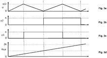
- Fig. 3 shows diagrams comprising curves illustrating the functionality explained above.
- the horizontal axes may be interpreted as time axes.
- the curve in Fig. 3a shows alternating increases and decreases in the differential phase ⁇ from zero to ⁇ /2 and ⁇ /2 to zero, respectively.
- Figs. 3b and 3c show the values of the additional phase shifts ⁇ 2 and ⁇ 3 and Fig. 3d shows the steady increase in the total phase ⁇ out,1.
- the table in Fig. 2b shows the corresponding values for the additional phase shifts ⁇ 2 and ⁇ 3 and the total phase shift ⁇ out,2.
- Fig. 4 shows another embodiment 200 of an optical endless phase shifting device which differs from the embodiment 100 according to Fig. 1 only in that no optical phase shifter is provided in the second branch of the second stage 104. That is, the equations 1 to 6 may be used to describe the respective signals if the phase shift ⁇ 3 is set to zero.
- the full range from zero to 2 ⁇ can be divided in only two sections, namely, from zero to ⁇ and from ⁇ to 2 ⁇ , and thus a phase shift range for the differential phase shift ⁇ of [0; ⁇ ] is required for the optical phase shifters 110, 112.
- the optical endless phase shifting device 200 generally works in the same way as the optical endless phase shifting device 100 shown in Fig. 1 .
- the switching actions required to obtain an endless phase shifting are carried out or initiated by the control device 106 in such a way that the control device 106 creates a control signal S ⁇ 2 that is appropriate to switch the phase shift created by the phase shifter 118 from zero to ⁇ when the differential phase ⁇ reaches ⁇ , and the control device 106 creates a control signal S ⁇ 2 that is appropriate to switch the phase shift created by the phase shifter 118 from ⁇ to zero when the differential phase ⁇ reaches zero.
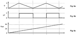
- Fig. 6 shows diagrams comprising curves illustrating the endless phase switching capability of the optical endless phase switching device 200 explained above.
- the horizontal axes may be interpreted as time axes.
- the curve in Fig. 6a shows alternating increases and decreases in the differential phase ⁇ from zero to ⁇ and ⁇ to zero, respectively.
- Figs. 6b shows the values of the additional phase shift ⁇ 2 and
- Fig. 6c shows the steady increase in the total phase ⁇ out,1.
- All embodiments 100, 200 of the invention provide an endless switching capability wherein the switching operations are performed at times at which the optical power of the optical signal that is supplied to the input port of the respective optical phase shifter is essentially zero or at least very low so that essentially no signal distortions occur. Only a single switching operation must be performed at a time so that no synchronization of two or more phase shifters is required.
Landscapes
- Physics & Mathematics (AREA)
- General Physics & Mathematics (AREA)
- Optics & Photonics (AREA)
- Nonlinear Science (AREA)
- Electromagnetism (AREA)
- Engineering & Computer Science (AREA)
- Computer Networks & Wireless Communication (AREA)
- Signal Processing (AREA)
- Optical Communication System (AREA)
- Optical Modulation, Optical Deflection, Nonlinear Optics, Optical Demodulation, Optical Logic Elements (AREA)
Abstract
Description
- The invention relates to an optical endless phase shifting device configured to shift an optical input signal by a desired phase shift as well as to a method therefore.
- The necessity of endless phase-shifting of an optical signal occurs in connection with various communication components, especially in connection with coherent detection. For coherent detection, the data signal received is superimposed with a local oscillator signal, for instance in an optical 3-dB coupler, and the combined signal is received on a photodiode. As compared to direct detection, coherent detection reveals an improved sensitivity for the detection of intensity-modulated optical signals. A drawback of coherent detection is the fact that the output electrical signal is also dependent on the phase difference between the optical signal to be received and the local oscillator signal with a sinusoidal function. If both even slightly differ in frequency, the electrical signal fades in and out with the combined frequency. One solution is the use of a phase diversity receiver, e.g. based on an optical hybrid. The drawback is the increased componentry, as the phase-diverse signals need to be received on multiple photodiodes and processed in parallel. It is therefore beneficial to directly control the phase of the local oscillator to match the phase of the data signal at the interference coupler (or have a fixed phase difference of π/2). This requires an optical phase shifter that can continuously rotate the phase of the local oscillator, even over many multiples of π, without the need to "reset" the phase, e.g. when the desired phase shift reaches a value equal to 2π or an integer multiple thereof.
- Another problem with coherent detection is also the fact that ideally the optical signal to be detected and the local oscillator signal need to have the same polarization for optimum interference. Of course, polarization diversity detection would solve this problem but, as mentioned above, requires additional componentry and signal processing to separate the signal to be detected into two signals of orthogonal polarization and to further process these signals. In order to avoid polarization diversity detection, an optical circuit realizing an optical polarization controller is required to convert the optical signal to be detected that has an arbitrary polarization into an optical signal having a predefined polarization, e.g. corresponding to the polarization supported by a waveguide structure in silicon, which supports only one polarization. Also such optical polarization controllers require an endless and reset-less phase control.
- A further application of an endless phase shifter is the stabilization of the phase of a laser. Supported by a PLL, comparing phase samples at different times, the endless phase shifter can be used to maintain a constant optical phase at the phase shifter output.
-
US 8,787,708 B2 discloses an endless phase shifting apparatus, structures and method useful, for example, in multiple-input multiple-output optical demultiplexers. Here, a phase modulator can create a phase shift between 0 and 4pi. A waveguide parallel to the phase modulator has a fixed phase delay of 2π. Optical switches before and after the structure allow to switch the signal between the phase modulator and the parallel waveguide. When the modulator is at 0 or 4π phase shift, the signal is switched to the parallel waveguide and the phase modulator is reset to a phase shift of 2π. Allegedly, this switching occurs without impact on the signal. However, simultaneously switching the optical switches before and after the phase modulator is a challenging task. Thus, the main drawbacks of this method and device for endless shifting an optical signal are that the phase modulator must provide a large phase shift range of 4π and that fast switches and a fast modulator phase reset are required. - An alternative endless phase shifter can be realized by an IQ-modulator structure, wherein in-phase and quadrature components are modulated, maintaining a constant amplitude and introducing a phase rotation. While this setup can continuously modulate the phase without fast switching or a fast phase reset, the intrinsic insertion loss is 6 dB, which in many cases cannot be tolerated.
- It is thus an object of the present invention to provide an optical endless phase shifting device for phase shifting an optical input signal by a desired phase shift which reveals a lower intrinsic insertion loss and which does not require synchronous fast switching. It is a further object of the present invention to provide a method for realizing such an optical endless phase shifting device.
- The invention achieves these objects with the combination of features of the
independent claims 1 and 14, respectively. - According to the invention, the optical endless phase shifting device comprises a first and a second stage. The first stage comprises a Mach-Zehnder structure comprising a passive optical splitter device configured to receive, at an input port, an optical input signal (Ein) and to split the input signal into a first and a second partial signal, each of which is fed, from a dedicated output port of the splitter device, to a first and a second branch of the first stage that connects the respected output port of the splitter device to a dedicated input port of a passive optical combiner device, the combiner device being configured to output a first combined signal at a first output port and a second combined signal at a second output port, each of the first and second branches of the first stage comprising a controllable optical phase shifter, wherein the phase shifter in the first branch is configured to shift the phase of the first partial signal by a positive predetermined phase shift and wherein the phase shifter in the second branch is configured to shift the phase of the second partial signal by a negative predetermined phase shift. In other words, the first stage realizes a Mach-Zehnder interferometer with push-pull configuration using an optical 2x2-coupler for creating two optical signals that are fed to the second stage. The second stage comprises a passive optical combiner device having a first input port connecting a first branch of the second stage to the first output port of the first stage combiner device and a second input port connecting a second branch of the second stage to the second output port of the first stage combiner device, the first branch or the first and second branches of the second stage comprising a controllable optical phase shifter, the combiner device being configured to output, at at least one output port, an optical output signal, which corresponds to the optical input signal that is phase-shifted by the desired phase shift.
- According to the invention, the optical phase shifters in the first branch or the first and second branches of the second stage are configured to be switchable between a first value of zero and a second value of π for a phase shift created by the respective optical phase shifter. As apparent from the following description, the optical phase shifters in the first or the first and the second branches are switched, in order to provide the endless phase-shifting capability of the device, in a status in which the optical power of the signal in the respective branch is essentially zero. This mitigates the requirement of providing high-speed and high-precision switching.
- In order to provide an endless phase shifting capability, the first stage optical phase shifters are controllable in such a way that that they create a predetermined phase shift having an absolute value within a range from 0 to π/2 in case an optical phase shifter is provided in both branches of the second stage, or that they create a predetermined phase shift having an absolute value within a range from 0 to π in case an optical phase shifter is provided in only the first branch of the second stage.
- That is, in embodiments that comprise a phase shifter in both branches of the second stage, the phase-shift range of the phase shifters of the first stage can be restricted to a small range from zero to π/2. The endless-shifting capability of the device is achieved by switching the two phase shifters of the second stage into an appropriate status of zero or π, respectively, when, depending on the desired (total) phase shift, the absolute value of predetermined phase shift that is to be realized by each of the two phase shifters of the first stage reaches the upper or lower boundary of the phase shift range from zero to π/2. As will become apparent from the description below, the neighboring status of the two switches of the second stage requires switching of only one of the phase shifters from zero to π or from π to zero, wherein the optical power of the signal present in the branch in which the phase shifter to be switched is provided is zero.
- Generally the same applies to embodiments that comprise a phase shifter in the first branch of the second stage only. In this first branch, the optical signal is proportional to the sine of the (positive) phase shift (or phase angle) created by phase shifters comprised in the branches of the first stage. However, these embodiments require a larger phase shift range for the predetermined phase shift from zero to π.
- According to an embodiment of the invention, the optical splitter device that is comprised by the first stage may be configured to output a first and a second optical output signal, wherein the electrical fields of the first and second optical output signals have essentially the same absolute value, but are shifted by π/2.
- This property is in general fulfilled by an optical 1x2 coupler, e.g. an optical 1x2 fiber coupler or an optical integrated 1x2 coupler. In such optical couplers, the electrical field of the optical signal that is coupled from a pass-through path to the further output path is rotated by π/2.
- According to an embodiment, the optical combiner devices of the first and or second stage may be configured to create the first combined signal (Esin) by adding the electrical field of the optical signal that is fed to the first input port and the electrical field of the optical signal that is fed to the second input port shifted by π/2, and the second combined signal (Ecos) by adding the electrical field of the optical signal that is fed to the second input port and the electrical field of the optical signal that is fed to the first input port shifted by π/2.
- Such an optical combiner device may be realized as an optical 1x2 coupler, e.g. an optical 1x2 fiber coupler or an optical integrated 1x2 coupler.
- According to an embodiment, the first stage combiner device may be configured to create, at the first and second output port, the first and second combined signals (Esin, Ecos) in such a way that they can be described by


- The second stage combiner device may be configured to create, at the at least one output port, the at least one optical output signal in such a way that it can be described by


- According to the invention, the endless phase shifting device may comprise a control device configured to receive a phase shift signal including the desired phase shift and to output control signals that are fed to the phase shifters of the first stage as well as one or two control signals that are fed to the one or two phase shifters of the second stage.
- According to an embodiment of the invention, a phase shifter is provided in both branches of the second stage and the at least one optical output signal is created according to the
above alternative 1. In this embodiment, the control device can be configured to create the control signals in such a way - that the optical phase shifters in both branches of the second stage create a phase shift zero if the desired phase shift is within a range from zero to π/2 plus a positive integer times 2π,
- that the optical phase shifter in the first branch of the second stage creates a phase shift zero and the optical phase shifter in the second branch of the second stage creates a phase shift π if the desired phase shift is within a range from π/2 to π plus a positive integer times 2π,
- that the optical phase shifters in both branches of the second stage create a phase shift π if the desired phase shift is within a range from π to 3/2·π plus a positive integer times 2π, and
- that the optical phase shifter in the first branch of the second stage creates a phase shift π and the optical phase shifter in the second branch of the second stage creates a phase shift zero if the desired phase shift is within a range from 3/2·π to 2π plus a positive integer times 2π.
- According to another embodiment of the invention, a phase shifter is provided in both branches of the second stage and the at least one optical output signal is created according to the
above alternative 2. In this embodiment, the control device can be configured create to the control signals in such a way - • that the optical phase shifter in the first branch of the second stage creates a phase shift π and the optical phase shifter in the second branch of the second stage creates a phase shift zero if the desired phase shift is within a range from zero to π/2 plus a positive integer times 2π,
- • that the optical phase shifters in both branches of the second stage create a phase shift π if the desired phase shift is within a range from π/2 to π plus a positive integer times 2π,
- • that the optical phase shifter in the first branch of the second stage creates a phase shift zero and the optical phase shifter in the second branch of the second stage creates a phase shift π if the desired phase shift is within a range from π to 3/2·π plus a positive integer times 2π, and
- • that the optical phase shifters in both branches of the second stage create a phase shift zero if the desired phase shift is within a range from 3/2·π to 2π plus a positive integer times 2π.
- In further embodiments, in which a phase shifter is provided in the first branch of the second stage only and the at least one optical output signal is created according to the
above alternative 1, the control device can be configured to create the control signals in such a way that the optical phase shifter of the second stage creates a phase shift zero if the desired phase shift is within a range from zero to π plus a positive integer times 2π, and that the optical phase shifter of the second stage creates a phase shift π if the desired phase shift is within a range from π to 2π plus a positive integer times 2π. - In embodiments in which a phase shifter is provided in the first branch of the second stage only and the at least one optical output signal is created according to the
above alternative 2, the control device can be configured to create the control signals in such a way that the optical phase shifter of the second stage creates a phase shift π if the desired phase shift is within a range from zero to π plus a positive integer times 2π, and that the optical phase shifter of the second stage creates a phase shift zero if the desired phase shift is within a range from π to 2π plus a positive integer times 2π. - According to an embodiment, the method for endless shifting of an optical input signal by a desired phase shift according to the invention comprises the steps of:
- splitting the optical input signal (Sin) and phase shifting the split optical input signals by a predetermined positive and negative phase shift (+ϕ, -ϕ), respectively, wherein the absolute value (ϕ) of the predetermined phase shift lies within a range of zero and π/2;
- creating a first combined optical signal (Ssin) by further phase shifting at least one of the phase-shifted signals and adding the further phase-shifted signals, wherein the further phase shift is chosen in such a way that the first combined signal (Ssin) is proportional to Ein·sin(ϕ), wherein Ein designates the complex amplitude of the electrical field of the optical input signal (Sin);
- creating a second combined optical (Scos) signal by further phase shifting at least one of the phase-shifted signals and adding the further phase-shifted signals, wherein the further phase shift is chosen in such a way that the second combined signal is proportional to Ein·cos(ϕ);
- phase-shifting the first combined optical signal (Ssin) by a selectable value for a first additional phase shift (ϕ2) of zero or π and phase-shifting the second combined optical signal by a selectable value for a second additional phase shift (ϕ3) of zero or π;
- creating at least one optical output signal (Sout,1, Sout,2) by adding the first and second additionally phase-shifted combined signals, wherein the first and/or second combined signal reveal a phase relation or wherein the first and/or second combined signals are further phase-shifted in such a way that the complex amplitude of the electrical signal of the optical output signal (Sout,1, Sout,2) is proportional to
- ∘

- ∘

- ∘
- selecting the first and second additional phase shift (ϕ2, ϕ3), depending on the desired phase shift (ϕtot) and the absolute value (ϕ) of the predetermined phase shift (+ϕ, -ϕ), if the at least one optical output signal (Sout,1, Sout,2) is created according to
alternative 1, as follows:- selecting a value of zero for both additional phase shifts (ϕ2, ϕ3) if the desired phase shift (ϕtot) is within a range from zero to π/2 plus a positive integer times 2π;
- selecting a value of zero for the first additional phase shift (ϕ2) and a value of π for the second additional phase shifts (ϕ3) if the desired phase shift (ϕtot) is within a range from π/2 to π plus a positive integer times 2π;
- selecting a value of π for both additional phase shifts (ϕ2, ϕ3) if the desired phase shift (ϕtot) is within a range from π to 3/2·π plus a positive integer times 2π, and
- selecting a value of π for the first additional phase shifts (ϕ2) and a value of zero for the second additional phase shifts (ϕ3) if the desired phase shift (ϕtot) is within a range from 3/2•π to 2π plus a positive integer times 2π; or
- selecting the first and second additional phase shift (ϕ2, ϕ3), depending on the desired phase shift (ϕtot) and the absolute value (ϕ) of the predetermined phase shift (+ϕ, -ϕ) if the at least one optical output signal (Sout,1, Sout,2) is created according to
alternative 2, as follows:- selecting a value of π for the first additional phase shift (ϕ2) and a value of zero for the second additional phase shift (ϕ3) if the desired phase shift (ϕtot) is within a range from zero to π/2 plus a positive integer times 2π;
- selecting a value of π for both additional phase shifts (ϕ2, ϕ3) if the desired phase shift (ϕtot) is within a range from π/2 to π plus a positive integer times 2π;
- selecting a value of zero for the first additional phase shift (ϕ2) and a value of π for the second additional phase shifts (ϕ3) if the desired phase shift (ϕtot) is within a range from π to 3/2·π plus a positive integer times 2π, and
- selecting a value of zero for both additional phase shifts (ϕ2, ϕ3) if the desired phase shift (ϕtot) is within a range from 3/2·π to 2π plus a positive integer times 2π.
- According to another embodiment, the method for endless shifting of an optical input signal by a desired phase shift according to the invention comprises the steps of:
- splitting the optical input signal (Sin) and phase-shifting the split optical input signals by a predetermined positive and negative phase shift (+ϕ, -ϕ), respectively, wherein the absolute value (ϕ) of the predetermined phase shift lies within a range of zero and π/2;
- creating a first combined optical signal (Ssin) by further phase-shifting at least one of the phase shifted signals and adding the further phase-shifted signals, wherein the further phase shift is chosen in such a way that the first combined signal (Ssin) is proportional to Ein·sin(ϕ), wherein Ein designates the complex amplitude of the electrical field of the optical input signal (Sin);
- creating a second combined optical signal (Scos) by further phase-shifting at least one of the phase-shifted signals and adding the further phase-shifted signals, wherein the further phase shift is chosen in such a way that the second combined signal is proportional to Ein·cos(ϕ);
- phase-shifting the first combined optical signal (Ssin) by a selectable value for an additional phase shift (ϕ2) of zero or π;
- creating at least one optical output signal (Sout,1, Sout,2) by adding the first additionally phase-shifted combined signal and the second combined signal, wherein the first and/or second combined signals reveal a phase relation or wherein the first and/or second combined signals are further phase shifted in such a way that the complex amplitude of the electrical signal of the optical output signal (Sout,1, Sout,2) is proportional to
- ∘

- ∘

- ∘
- selecting the additional phase shift (ϕ2), depending on the desired phase shift (ϕtot) and the absolute value (ϕ) of the predetermined phase shift (+ϕ, -ϕ) if the at least one optical output signal (Sout,1, Sout,2) is created according to
alternative 1, as follows:- selecting a value of zero for the additional phase shift (ϕ2) if the desired phase shift (ϕtot) is within a range from zero to π plus a positive integer times 2π;
- selecting a value of π for the additional phase shift (ϕ2) if the desired phase shift (ϕtot) is within a range from π to 2·π plus a positive integer times 2π, or
- selecting the additional phase shift (ϕ2), depending on the desired phase shift (ϕtot) and the absolute value (ϕ) of the predetermined phase shift (+ϕ, -ϕ) if the at least one optical output signal (Sout,1, Sout,2) is created according to
alternative 2, as follows:- selecting a value of π for the additional phase shift (ϕ2) if the desired phase shift (ϕtot) is within a range from zero to π plus a positive integer times 2π;
- selecting a value of zero for the additional phase shift (ϕ2) if the desired phase shift (ϕtot) is within a range from π to 2·π plus a positive integer times 2π.
- These and other features and objects of the present invention will become more fully apparent from the following description of specific embodiments thereof which are illustrated in the drawings. It is appreciated that these drawings depict only typical embodiments of the invention and are therefore not to be considered limiting of its scope. The invention will be described and explained with additional specificity and detail through the use of the accompanying drawings in which:
- Fig. 1
- shows a schematic block diagram of a first embodiment of an optical endless phase shifting device according to the present invention comprising optical phase shifters in both branches of the second stage;
- Fig. 2
- shows tables including values of the phase shifts created by the optical phase shifters and the values for the resulting phase shift of the phase-shifted optical output signals of the second stage of the embodiment according to
Fig. 1 ; - Fig. 3
- shows, for the embodiment according to
Fig. 1 , diagrams comprising curves for the phase shift ϕ created by the optical phase shifters of the first stage (Fig. 3a ), for the phase shifts ϕ2, ϕ3 created by the optical phase shifters of the first and second branch of the second stage (Figs. 3b, 3c ) and for the total phase shift of the phase-shifted optical output signals of the second stage (Fig. 3d ); - Fig. 4
- shows a schematic block diagram of a second embodiment of an optical endless phase shifting device according to the present invention comprising optical phase shifters in the first branch of the second stage only;
- Fig. 5
- shows tables including values of the phase shifts created by the optical phase shifter and the values for the resulting phase shift of the phase-shifted optical output signals of the second stage of the embodiment according to
Fig. 4 ; - Fig. 6
- shows, for the embodiment according to
Fig. 1 , diagrams comprising curves for the phase shift ϕ created by the optical phase shifters of the first stage (Fig. 6a ), for the phase shift ϕ2 created by the optical phase shifter of the first branch of the second stage (Fig. 6b ) and for the total phase shift ϕtot of the phase-shifted optical output signals of the second stage (Fig. 6c ). -
Fig. 1 shows a schematic block diagram of a first embodiment of an optical endlessphase shifting device 100 comprising afirst stage 102 and asecond stage 104. Both stages are controlled by acontrol device 106. - The first stage comprises a Mach-Zehnder interferometer structure that is operated in push-pull configuration and that comprises a passive 1x2
optical splitter device 108, two controllableoptical phase shifters optical combiner device 114. The two controllableoptical phase shifters optical splitter device 108 and a first input port of the passiveoptical combiner device 114, and the second branch extends between a second splitting port of the passiveoptical splitter device 108 and a second input port of the passiveoptical combiner device 114. - The passive 1x2
optical splitter device 108 may be realized as a passive optical 1x2 fiber coupler or any other type of passive optical 1x2 coupler, e.g. an integrated waveguide coupler. Likewise, the passive 2x2optical combiner device 114 may be realized as a passive optical 2x2 fiber coupler or any other type of passive optical 2x2 coupler, e.g. an integrated waveguide coupler. Each of the two controllable phase shifters, which may be realized in any arbitrary way, is configured to create a predetermined phase shift between an optical input signal received at an input port and an optical output signal output at an output port depending on a control signal S+ϕ, S-ϕ, e.g. a voltage, that is fed to a respective control port. Generally, thephase shifters control device 106, in such a way that a positive predetermined phase shift +ϕ is created by thephase shifter 110 and a negative predetermined phase shift -ϕ is created by thephase shifter 112. In case of the embodiment according toFig. 1 , thephase shifters control device 106 are configured to create a positive and negative phase shift with an absolute value of ϕ in the range of [0; π/2] depending on the respective control signal S+ϕ, S-ϕ that is supplied to the corresponding opticalphase shifter device control device 106. In the following, the absolute value of the predetermined phase shift -ϕ, +ϕ is also referred to as differential phase shift. - The second stage comprises a further passive optical
2x2 combiner device 116 and two further controllableoptical phase shifters optical phase shifters optical combiner device 114 of the first stage and a first input port of the passiveoptical combiner device 116, and the second branch extends between a second output port of the passiveoptical combiner device 114 of the first stage and a second input port of the passiveoptical combiner device 116. Each of thephase shifters control device 106. - It shall be noted that the whole optical endless
phase shifting device 100 may be realized as a photonic integrated circuit (PIC). - In the following, the function of the endless
phase shifting device 100 will be explained in detail. - An optical input signal Sin, e.g. the optical signal created by a local oscillator of a coherent optical receiver, which is characterized by a complex amplitude Ein, is fed to an input port of the passive
optical splitter device 108. The endlessphase shifting device 100 creates at least one optical output signal Sout,1, Sout,2, which is output at a respective output port of the passiveoptical combiner device 116 of thesecond stage 104, wherein the at least one output signal Sout,1, Sout,2 corresponds to the optical input signal Sin but is phase-shifted by a predetermined total phase shift ϕtot. In the following, the total phase shift ϕtot is also referred to as "desired phase shift". - The passive optical
1x2 splitter device 108, which is preferably a 3dB splitter device, splits the input signal Sin into two signals that are phase-shifted between each other by π/2 due to an inherent property of the passiveoptical splitter device 108. These signals are then shifted, by the respectiveoptical phase shifter 2x2 combiner device 114, which is preferably realized as a 3dB 2x2 combiner device, into two combined signals Ssin and Scos (each represented by the complex amplitude of the electric field Esin and Ecos). Thecombiner device 114 also adds an additional phase shift of π/2 to one of the two components that are added to yield the signals Ssin and Scos. It can be shown that the following equations describe the signals Ssin and Scos:

- Obviously, these signals are proportional to the cosine and the sine of the differential phase shift, respectively.
- In the second stage, the signals Ssin and Scos are phase-shifted, by the respective
optical phase shifter optical combiner device 116, into the at least one output signal Sout,1, Sout,2, wherein thecombiner device 116 adds an additional phase shift of π/2 to one of the two components that are added to yield the at least one output signal Sout,1, Sout,2. In the embodiment ofFig. 1 , two output signals Sout,1, Sout,2 are created by the2x2 combiner device 116, which is used in the second stage. It is, however, also possible to use a 2x1 combiner device in the second stage so that only a single output signal (i.e. either Sout,1 or Sout,2) is created. Usingequations 

optical phase shifters 

Fig. 2a shows the values for the total phase shift ϕout,1 for all possible combinations of the phase shifts created by thephase shifters second stage 104. If both phase shifts ϕ2, ϕ3 are zero, the total phase shift (ϕout,1 equals the differential phase shift ϕ, i.e. the total phase shift ϕout,1 varies from zero to π/2 if the differential phase shift is varied from zero to π/2. When the total phase shift (ϕout,1 reaches π/2, the phase shift ϕ3 is switched to π. Thus, reducing the differential phase shift from π/2 to zero leads to a further increase in the total phase shift ϕout,1, as now the total phase shift (ϕout,1 equals (π-ϕ). When the differential phase shift reaches zero, the phase shift ϕ2 is switched to π (while ϕ3 is kept at π). Thus, if the differential phase shift ϕ is again increased from zero to π/2, the total phase shift (ϕout,1 further increases from π to 3/2·π, as now the total phase shift (ϕout,1 equals (π+ϕ). When the differential phase reaches π/2, the phase shift ϕ3 is switched to zero (while ϕ2 is kept at π). Therefore, a decrease in the differential phase shift from π/2 to zero again leads to a further increase in the total phase shift ϕout,1, as now the total phase shift (ϕout,1 equals (2π-ϕ), which is identical to -ϕ. If the differential phase ϕ is again increased from zero to π/2, i.e. the total phase shift equals 2π+ϕ, the phase shift ϕ2 is switched to zero (while ϕ3 is kept at zero) and the cycle is repeated from the beginning. That is, the values for the total phase shift ϕout,1 in the now beginning cycle can be calculated by the values given in the table inFig. 2a plus 2π (in general, for each additional cycle 2π must be added to the values for ϕout,1 given in the table according toFig. 2a ). In this way an endless shift of the total phase shift ϕout,1 can be realized by appropriately switching the values of the phase shift ϕ2 and ϕ3 from zero to π or vice versa at the borders of the range of [0;π/2] for the differential phase shift ϕ. - Of course, the value of the differential phase shift ϕ instead of the value of the total phase shift ϕout,1 or ϕout,2 can be used in order to determine when a switching operation of the
phase shifters - As the switching of the additional phase shifts ϕ2 and ϕ3 is carried out in a state when the power in the respective branch of the
second stage 104 is (nearly) zero, a phase shift in this branch between zero and π can be created without disturbing the optical signal. - The
control device 106 may be configured to create the control signals Sϕ2, Sϕ3 depending on the values of the differential phase shift ϕ, i.e. at a time when the differential phase shift ϕ reaches the upper or lower limit value of the range for the differential phase shift ϕ, the control signals Sϕ2, Sϕ3 comprise features (e.g. a rising or falling edge) that trigger a switching operation of one of thephase shifters - The control device may be configured to receive a phase control signal Sϕctrl comprising information concerning a value for the total phase shift ϕtot (i.e. for the phase shifts ϕout,1 and/or ϕout,2 of the optical output signals Sout,1 and/or Sout,2, respectively). Theoretically, if the value for the total phase shift ϕtot is larger than 2π, the control device may start at an arbitrary value smaller than 2π and increase the total phase shift (by appropriately increasing the differential phase shift ϕ and performing the switching operations of the
phase shifters 118, 120) until the desired total phase shift ϕtot is reached. However, as in most applications the optical input signal is a narrow band signal (e.g. a CW laser signal), a start value for the total phase will generally be chosen in such a way that it lies within [0;2π] as any higher value that is equal to such a start value plus an integer value times 2π will lead to the same result due to the periodicity of the optical input signal Sin. -
Fig. 3 shows diagrams comprising curves illustrating the functionality explained above. The horizontal axes may be interpreted as time axes. The curve inFig. 3a shows alternating increases and decreases in the differential phase ϕ from zero to π/2 and π/2 to zero, respectively.Figs. 3b and 3c show the values of the additional phase shifts ϕ2 and ϕ3 andFig. 3d shows the steady increase in the total phase ϕout,1. - The table in
Fig. 2b shows the corresponding values for the additional phase shifts ϕ2 and ϕ3 and the total phase shift ϕout,2. Again, the four quadrants of a total phase shift of 2π for the output signal Sout,2 can be realized by starting with ϕ2=π, ϕ3=0 in the first quadrant, in which 0≤ϕ≤π/2, switching to ϕ2=π, ϕ3=π when ϕ=π/2 and keeping these values of ϕ2, ϕ3 in the second quadrant, in which π/2≤ϕ≤π, switching to ϕ2=0, ϕ3=π when ϕ=π and keeping these values of ϕ2, ϕ3 in the third quadrant, in which π≤ϕ≤3/2·π, and switching to ϕ2=0, ϕ3=0 when ϕ=3/2·π and keeping these values of ϕ2, ϕ3 in the fourth quadrant, in which 3/2·π ≤ϕ≤2π, and so on in the following cycles.Fig. 4 shows anotherembodiment 200 of an optical endless phase shifting device which differs from theembodiment 100 according toFig. 1 only in that no optical phase shifter is provided in the second branch of thesecond stage 104. That is, theequations 1 to 6 may be used to describe the respective signals if the phase shift ϕ3 is set to zero. As only two states are possible by switching the singleoptical phase shifter 118 between zero and π, the full range from zero to 2π can be divided in only two sections, namely, from zero to π and from π to 2π, and thus a phase shift range for the differential phase shift ϕ of [0;π] is required for theoptical phase shifters phase shifting device 200 generally works in the same way as the optical endlessphase shifting device 100 shown inFig. 1 . - The switching actions required to obtain an endless phase shifting are carried out or initiated by the
control device 106 in such a way that thecontrol device 106 creates a control signal Sϕ2 that is appropriate to switch the phase shift created by thephase shifter 118 from zero to π when the differential phase ϕ reaches π, and thecontrol device 106 creates a control signal Sϕ2 that is appropriate to switch the phase shift created by thephase shifter 118 from π to zero when the differential phase ϕ reaches zero. - As shown in the tables according to
Fig. 5 , the total phase shift ϕout,1 is equal to the differential phase shift ϕ (plus an integer value times 2π) if thephase shifter 118 creates a phase shift of ϕ2=0 and equal to 2π minus the differential phase shift ϕ (i.e. equal to -ϕ) (plus an integer value times 2π) if thephase shifter 118 creates a phase shift of ϕ2=π (Fig. 5a ). The total phase shift ϕout,2 is equal to the differential phase shift ϕ (plus an integer value times 2π) if thephase shifter 118 creates a phase shift of ϕ2=π and equal to 2π minus the differential phase shift ϕ (i.e. equal to -ϕ) (plus an integer value times 2π) if thephase shifter 118 creates a phase shift of ϕ2=0 (Fig. 5b ). -
Fig. 6 shows diagrams comprising curves illustrating the endless phase switching capability of the optical endlessphase switching device 200 explained above. The horizontal axes may be interpreted as time axes. The curve inFig. 6a shows alternating increases and decreases in the differential phase ϕ from zero to π and π to zero, respectively.Figs. 6b shows the values of the additional phase shift ϕ2 andFig. 6c shows the steady increase in the total phase ϕout,1. - All
embodiments -
- 100
- optical endless phase shifting device
- 102
- first stage
- 104
- second stage
- 106
- control device
- 108
- passive optical splitter device
- 110
- optical phase shifter
- 112
- optical phase shifter
- 114
- passive optical combiner device
- 116
- passive optical combiner device
- 118
- optical phase shifter
- 120
- optical phase shifter
- ϕ
- differential phase shift / predetermined phase shift
- +ϕ
- phase shift
- -ϕ
- phase shift
- ϕ2
- additional phase shift
- ϕ3
- additional phase shift
- ϕtot
- total phase shift / desired phase shift
- Ein
- complex amplitude of the electrical field of Sin
- Esin
- complex amplitude of the electrical field of Ssin
- Ecos
- complex amplitude of the electrical field of Scos
- S+ϕ
- control signal
- S-ϕ
- control signal
- Sϕ2
- control signal
- Sϕ3
- control signal
- Sin
- optical input signal Sin
- Sout,1
- optical output signal
- Sout,2
- optical output signal
- Ssin
- combined signal
- Scos
- combined signal
- Sϕctrl
- control signal
Claims (15)
- Optical endless phase shifting device for shifting an optical input signal by a desired phase shift comprising a first (102) and a second stage (104),(a) the first stage (102) comprising a Mach-Zehnder structure comprising a passive optical splitter device (108) configured to receive, at an input port, an optical input signal (Sin) and to split the input signal into a first and a second partial signal, each of which is fed, from a dedicated output port of the splitter device (108), to a first and a second branch of the first stage (102) that connects the respective output port of the splitter device (108) to a dedicated input port of a passive optical combiner device (114), the combiner device (114) being configured to output a first combined signal (Ssin) at a first output port and a second combined signal (Ssin) at a second output port, each of the first and second branches of the first stage (102) comprising a controllable optical phase shifter (110, 112), wherein the phase shifter (110) in the first branch is configured to shift the phase of the first partial signal by a positive predetermined phase shift (+ϕ) and wherein the phase shifter (112) in the second branch is configured to shift the phase of the second partial signal by a negative predetermined phase shift (-ϕ), and(b) the second stage (104) comprising a passive optical combiner device (116) having a first input port connecting a first branch of the second stage (104) to the first output port of the first stage combiner device (114) and a second input port connecting a second branch of the second stage (104) to the second output port of the first stage combiner device (114), the first branch or the first and second branches of the second stage (104) comprising a controllable optical phase shifter (118, 120), the combiner device (116) being configured to output, at at least one output port, an optical output signal (Sout,1, Sout,2), which corresponds to the optical input signal (Sin) that is phase shifted by the desired phase shift (ϕtot),(c) wherein the optical phase shifters (118, 120) in the first branch or the first and second branches of the second stage (104) are configured to be switchable between a first value of zero and a second value of π for a phase shift created by the respective optical phase shifter (118, 120), and(d) wherein the first stage optical phase shifters (110, 120) are controllable in such a way(i) that they create a predetermined phase shift (+ϕ, -ϕ) having an absolute value within a range from 0 to π/2 in case an optical phase shifter (118, 120) is provided in both branches of the second stage (104), or(ii) that they create a predetermined phase shift (+ϕ, -ϕ) having an absolute value within a range from 0 to π in case an optical phase shifter (118) is provided in only the first branch of the second stage (104).
- Optical endless phase shifting device according to claim 1, characterized in that the optical splitter device (108) is configured to output a first and a second optical output signal, wherein the electrical fields of the first and second optical output signals have essentially the same absolute value but are phase shifted by π/2.
- Optical endless phase shifting device according to claim 2, characterized in that the optical splitter device (108) is an optical 1x2 coupler, e.g. an optical 1x2 fiber coupler or an optical integrated 1x2 coupler.
- Optical endless phase shifting device according to one of the preceding claims, characterized in that the optical combiner device (114) of the first stage (102) is configured to create(a) the first combined signal (Ssin) by adding the electrical field of the optical signal that is fed to the first input port and the electrical field of the optical signal that is fed to the second input port shifted by π/2, and(b) the second combined signal (Scos) by adding the electrical field of the optical signal that is fed to the second input port and the electrical field of the optical signal that is fed to the first input port phase-shifted by π/2.
- Optical endless phase shifting device according to one of the preceding claims, characterized in that the optical combiner device (116) of the second stage (104) is configured to create the at least one output signal (Sout,1, Sout,2)(a) by adding the electrical field of the optical signal that is fed to the first input port and the electrical field of the optical signal that is fed to the second input port phase-shifted by π/2, and/or(b) by adding the electrical field of the optical signal that is fed to the second input port and the electrical field of the optical signal that is fed to the first input port shifted by π/2.
- Optical endless phase shifting device according to claims 4 or 5, characterized in that the optical combiner device (114, 116) is an optical 1x2 coupler, e.g. an optical 1x2 fiber coupler or an optical integrated 1x2 coupler.
- Optical endless phase shifting device according to one of the preceding claims, characterized in that the first stage combiner device (114) is configured to create, at the first and second output port, the first and second combined signals (Ssin, Scos) in such a way that they can be described by


- Optical endless phase shifting device according to claim 7, characterized in that the second stage combiner device (116) is configured to create, at the at least one output port, the at least one optical output signal (Sout,1, Sout,2) in such a way that it can be described by(a)
 (b)wherein Eout,1 and Eout,2 designate the complex field amplitude of two alternatives of the optical output signal (Sout,1, Sout,2), wherein ϕ2 designates the phase shift of zero or π created by a phase shifter (118) provided in the first branch of the second stage (104) and wherein ϕ3 designates the phase shift of zero or π created by a phase shifter (120) provided in the second branch of the second stage (104), and wherein the term ejϕ3 can be set to 1 if no phase shifter is provided in the second branch.
- Optical endless phase shifting device according to one of the preceding claims, characterized in that it comprises a control device (106) configured to receive a phase control signal (Sϕctrl) including information on the desired phase shift or a change thereof and to output control signals (S-ϕ, S+ϕ) that are fed to the phase shifters (110, 112) of the first stage (102) as well as one or two control signals (Sϕ2, Sϕ3) that are fed to the one or two phase shifters (118, 120) of the second stage (104).
- Optical endless phase shifting device according to claim 9, characterized in that a phase shifter (118, 120) is provided in both branches of the second stage (104), that the at least one optical output signal (Sout,1) is created according to feature (a) of claim 8 and that the control device (106) is configured to create the control signals (Sϕ2, Sϕ3) in such a way(a) that the optical phase shifters (118, 120) in both branches of the second stage (104) create a phase shift zero if the desired phase shift (ϕtot) is within a range from zero to π/2 plus a positive integer times 2π,(b) that the optical phase shifter (118) in the first branch of the second stage (104) creates a phase shift zero and the optical phase shifter (120) in the second branch of the second stage (104) creates a phase shift π if the desired phase shift (ϕtot) is within a range from π/2 to π plus a positive integer times 2π,(c) that the optical phase shifters (118, 120) in both branches of the second stage (104) create a phase shift π if the desired phase shift (ϕtot) is within a range from π to 3/2·π plus a positive integer times 2π, and(d) that the optical phase shifter (118) in the first branch of the second stage (104) creates a phase shift π and the optical phase shifter (120) in the second branch of the second stage (104) creates a phase shift zero if the desired phase shift (ϕtot) is within a range from 3/2·π to 2π plus a positive integer times 2π.
- Optical endless phase shifting device according to claim 10, characterized in that a phase shifter (120) is provided in both branches of the second stage (104), that the at least one optical output signal (Sout,2) is created according to feature (b) of claim 8 and that the control device (106) is configured create to the control signals (Sϕ2, Sϕ3) in such a way(a) that the optical phase shifter (118) in the first branch of the second stage (104) creates a phase shift π and the optical phase shifter in the second branch of the second stage creates a phase shift zero if the desired phase shift (ϕtot) is within a range from zero to π/2 plus a positive integer times 2π,(b) that the optical phase shifters (118, 120) in both branches of the second stage (104) create a phase shift π if the desired phase shift (ϕtot) is within a range from π/2 to π plus a positive integer times 2π,(c) that the optical phase shifter (118) in the first branch of the second stage (104) creates a phase shift zero and the optical phase shifter in the second branch of the second stage creates a phase shift π if the desired phase shift (ϕtot) is within a range from π to 3/2·π plus a positive integer times 2π, and(d) that the optical phase shifters (118, 120) in both branches of the second stage (104) create a phase shift zero if the desired phase shift (ϕtot) is within a range from 3/2·π to 2π plus a positive integer times 2π.
- Optical endless phase shifting device according to claim 10, characterized in that a phase shifter (118) is provided in the first branch of the second stage (104) only, that the at least one optical output signal (Sout,1) is created according to feature (a) of claim 8 and that the control device (106) is configured to create the control signal (Sϕ2) in such a way(a) that the optical phase shifter (118) of the second stage (104) creates a phase shift zero if the desired phase shift (ϕtot) is within a range from zero to π plus a positive integer times 2π, and(b) that the optical phase shifter (118) of the second stage (104) creates a phase shift π if the desired phase shift (ϕtot) is within a range from π to 2π plus a positive integer times 2π.
- Optical endless phase shifting device according to claim 10, characterized in that a phase shifter is provided in the first branch of the second stage only, that the at least one optical output signal (Sout,2) is created according to feature (b) of claim 8 and that the control device (106) is configured to create the control signal (Sϕ2) in such a way(a) that the optical phase shifter (118) of the second stage (104) creates a phase shift π if the desired phase shift (ϕtot) is within a range from zero to π plus a positive integer times 2π, and(b) that the optical phase shifter (118) of the second stage creates a phase shift zero if the desired phase shift (ϕtot) is within a range from π to 2π plus a positive integer times 2π.
- Method for endless shifting of an optical input signal by a desired phase shift comprising the steps of:(a) splitting the optical input signal (Sin) and phase shifting the split optical input signals by a predetermined positive and negative phase shift (+ϕ, -ϕ), respectively, wherein the absolute value (ϕ) of the predetermined phase shift lies within a range of zero and π/2;(b) creating a first combined optical signal (Ssin) by further phase shifting at least one of the phase-shifted signals and adding the further phase-shifted signals, wherein the further phase shift is chosen in such a way that the first combined signal (Ssin) is proportional to Ein·sin(ϕ), wherein Ein designates the complex amplitude of the electrical field of the optical input signal (Sin);(c) creating a second combined optical (Scos) signal by further phase shifting at least one of the phase-shifted signals and adding the further phase-shifted signals, wherein the further phase shift is chosen in such a way that the second combined signal is proportional to Ein·cos(ϕ);(d) phase-shifting the first combined optical signal (Ssin) by a selectable value for a first additional phase shift (ϕ2) of zero or π and phase-shifting the second combined optical signal by a selectable value for a second additional phase shift (ϕ3) of zero or π;(e) creating at least one optical output signal (Sout,1, Sout,2) by adding the first and second additionally phase-shifted combined signals, wherein the first and/or second combined signal reveal a phase relation or wherein the first and/or second combined signals are further phase-shifted in such a way that the complex amplitude of the electrical signal of the optical output signal (Sout,1, Sout,2) is proportional to(i)
 (ii)wherein j designates the imaginary unit; and
 (f) selecting the first and second additional phase shift (ϕ2, ϕ3), depending on the desired phase shift (ϕtot) and the absolute value (ϕ) of the predetermined phase shift (+ϕ, -ϕ), if the at least one optical output signal (Sout,1, Sout,2) is created according to alternative 1, as follows:(i) selecting a value of zero for both additional phase shifts (ϕ2, ϕ3) if the desired phase shift (ϕtot) is within a range from zero to π/2 plus a positive integer times 2π;(ii) selecting a value of zero for the first additional phase shift (ϕ2) and a value of π for the second additional phase shifts (ϕ3) if the desired phase shift (ϕtot) is within a range from π/2 to π plus a positive integer times 2π;(iii) selecting a value of π for both additional phase shifts (ϕ2, ϕ3) if the desired phase shift (ϕtot) is within a range from π to 3/2·π plus a positive integer times 2π, and(iv) selecting a value of π for the first additional phase shifts (ϕ2) and a value of zero for the second additional phase shifts (ϕ3) if the desired phase shift (ϕtot) is within a range from 3/2•π to 2π plus a positive integer times 2π; or(g) selecting the first and second additional phase shift (ϕ2, ϕ3), depending on the desired phase shift (ϕtot) and the absolute value (ϕ) of the predetermined phase shift (+ϕ, -ϕ) if the at least one optical output signal (Sout,1, Sout,2) is created according to alternative 2, as follows:(i) selecting a value of π for the first additional phase shift (ϕ2) and a value of zero for the second additional phase shift (ϕ3) if the desired phase shift (ϕtot) is within a range from zero to π/2 plus a positive integer times 2π;(ii) selecting a value of π for both additional phase shifts (ϕ2, ϕ3) if the desired phase shift (ϕtot) is within a range from π/2 to π plus a positive integer times 2π;(iii) selecting a value of zero for the first additional phase shift (ϕ2) and a value of π for the second additional phase shifts (ϕ3) if the desired phase shift (ϕtot) is within a range from π to 3/2·π plus a positive integer times 2π, and(iv) selecting a value of zero for both additional phase shifts (ϕ2, ϕ3) if the desired phase shift (ϕtot) is within a range from 3/2·π to 2π plus a positive integer times 2π.
 - Method for endless shifting of an optical input signal by a desired phase shift comprising the steps of:(a) splitting the optical input signal (Sin) and phase-shifting the split optical input signals by a predetermined positive and negative phase shift (+ϕ, -ϕ), respectively, wherein the absolute value (ϕ) of the predetermined phase shift lies within a range of zero and π/2;(b) creating a first combined optical signal (Ssin) by further phase-shifting at least one of the phase shifted signals and adding the further phase-shifted signals, wherein the further phase shift is chosen in such a way that the first combined signal (Ssin) is proportional to Ein·sin(ϕ), wherein Ein designates the complex amplitude of the electrical field of the optical input signal (Sin);(c) creating a second combined optical signal (Scos) by further phase-shifting at least one of the phase-shifted signals and adding the further phase-shifted signals, wherein the further phase shift is chosen in such a way that the second combined signal is proportional to Ein·cos(ϕ);(d) phase-shifting the first combined optical signal (Ssin) by a selectable value for an additional phase shift (ϕ2) of zero or π;(e) creating at least one optical output signal (Sout,1, Sout,2) by adding the first additionally phase-shifted combined signal and the second combined signal, wherein the first and/or second combined signals reveal a phase relation or wherein the first and/or second combined signals are further phase shifted in such a way that the complex amplitude of the electrical signal of the optical output signal (Sout,1, Sout,2) is proportional to(i)
 (ii)wherein j designates the imaginary unit; and
 (f) selecting the additional phase shift (ϕ2), depending on the desired phase shift (ϕtot) and the absolute value (ϕ) of the predetermined phase shift (+ϕ, -ϕ) if the at least one optical output signal (Sout,1, Sout,2) is created according to alternative 1, as follows:(i) selecting a value of zero for the additional phase shift (ϕ2) if the desired phase shift (ϕtot) is within a range from zero to π plus a positive integer times 2π;(ii) selecting a value of π for the additional phase shift (ϕ2) if the desired phase shift (ϕtot) is within a range from π to 2·π plus a positive integer times 2π, or(g) selecting the additional phase shift (ϕ2), depending on the desired phase shift (ϕtot) and the absolute value (ϕ) of the predetermined phase shift (+ϕ, -ϕ) if the at least one optical output signal (Sout,1, Sout,2) is created according to alternative 2, as follows:(i) selecting a value of π for the additional phase shift (ϕ2) if the desired phase shift (ϕtot) is within a range from zero to π plus a positive integer times 2π;(ii) selecting a value of zero for the additional phase shift (ϕ2) if the desired phase shift (ϕtot) is within a range from π to 2·π plus a positive integer times 2π.
Priority Applications (2)
| Application Number | Priority Date | Filing Date | Title |
|---|---|---|---|
| EP19194610.2A EP3786689B1 (en) | 2019-08-30 | 2019-08-30 | Method and device for endless phase shifting of an optical signal |
| US17/005,393 US11476948B2 (en) | 2019-08-30 | 2020-08-28 | Method and device for endless phase shifting of an optical signal |
Applications Claiming Priority (1)
| Application Number | Priority Date | Filing Date | Title |
|---|---|---|---|
| EP19194610.2A EP3786689B1 (en) | 2019-08-30 | 2019-08-30 | Method and device for endless phase shifting of an optical signal |
Publications (2)
| Publication Number | Publication Date |
|---|---|
| EP3786689A1 true EP3786689A1 (en) | 2021-03-03 |
| EP3786689B1 EP3786689B1 (en) | 2022-11-30 |
Family
ID=67874213
Family Applications (1)
| Application Number | Title | Priority Date | Filing Date |
|---|---|---|---|
| EP19194610.2A Active EP3786689B1 (en) | 2019-08-30 | 2019-08-30 | Method and device for endless phase shifting of an optical signal |
Country Status (2)
| Country | Link |
|---|---|
| US (1) | US11476948B2 (en) |
| EP (1) | EP3786689B1 (en) |
Cited By (1)
| Publication number | Priority date | Publication date | Assignee | Title |
|---|---|---|---|---|
| EP4550692A1 (en) | 2023-10-31 | 2025-05-07 | Adtran Networks SE | Processing of optical signals |
Citations (3)
| Publication number | Priority date | Publication date | Assignee | Title |
|---|---|---|---|---|
| US20120237156A1 (en) * | 2011-03-16 | 2012-09-20 | Nokia Siemens Networks Oy | Optical modulator, communication system, and communication method |
| US8787708B2 (en) | 2011-08-15 | 2014-07-22 | Alcatel Lucent | Endless phase shifting |
| US20150078702A1 (en) * | 2013-05-24 | 2015-03-19 | Futurewei Technologies, Inc. | System and Method for an Optical Phase Shifter |
Family Cites Families (1)
| Publication number | Priority date | Publication date | Assignee | Title |
|---|---|---|---|---|
| US6091864A (en) * | 1997-04-10 | 2000-07-18 | Ortel Corporation | Linear optical modulator for providing chirp-free optical signals |
-
2019
- 2019-08-30 EP EP19194610.2A patent/EP3786689B1/en active Active
-
2020
- 2020-08-28 US US17/005,393 patent/US11476948B2/en active Active
Patent Citations (3)
| Publication number | Priority date | Publication date | Assignee | Title |
|---|---|---|---|---|
| US20120237156A1 (en) * | 2011-03-16 | 2012-09-20 | Nokia Siemens Networks Oy | Optical modulator, communication system, and communication method |
| US8787708B2 (en) | 2011-08-15 | 2014-07-22 | Alcatel Lucent | Endless phase shifting |
| US20150078702A1 (en) * | 2013-05-24 | 2015-03-19 | Futurewei Technologies, Inc. | System and Method for an Optical Phase Shifter |
Non-Patent Citations (1)
| Title |
|---|
| CHRISTOPHER R DOERR: "Proposed Architecture for MIMO Optical Demultiplexing Using Photonic Integration", IEEE PHOTONICS TECHNOLOGY LETTERS, IEEE SERVICE CENTER, PISCATAWAY, NJ, US, vol. 23, no. 21, 1 November 2011 (2011-11-01), pages 1573 - 1575, XP011385615, ISSN: 1041-1135, DOI: 10.1109/LPT.2011.2164061 * |
Cited By (1)
| Publication number | Priority date | Publication date | Assignee | Title |
|---|---|---|---|---|
| EP4550692A1 (en) | 2023-10-31 | 2025-05-07 | Adtran Networks SE | Processing of optical signals |
Also Published As
| Publication number | Publication date |
|---|---|
| US20210067252A1 (en) | 2021-03-04 |
| EP3786689B1 (en) | 2022-11-30 |
| US11476948B2 (en) | 2022-10-18 |
Similar Documents
| Publication | Publication Date | Title |
|---|---|---|
| US9851615B2 (en) | Optical modulator | |
| CN110233675B (en) | Multifunctional microwave photonic module and signal processing method and device based thereon | |
| JP4170298B2 (en) | Optical receiver and optical reception method corresponding to differential four-phase shift keying | |
| JP2626896B2 (en) | Optical signal processing method and device, optical signal receiving method, and optical transmission device | |
| US8295710B2 (en) | Optical I-Q-modulator | |
| CN109842451B (en) | A Method for Photonic Frequency Conversion and Multi-Channel Phase Shift of Microwave Signal Using Dual Polarization Quadrature Phase Shift Keying Modulator | |
| US8295712B2 (en) | Optical device and method for optical frequency modulation to optical amplitude modulation conversion | |
| US10349155B2 (en) | Low-crosstalk electro-optical Mach-Zehnder switch | |
| US11646800B2 (en) | Optical transmitter and method for controller optical transmitter | |
| US8588337B2 (en) | Vector modulator | |
| US4829598A (en) | Optical receiver with an optical coupler and an electronic amplifier | |
| JP2008085889A (en) | Optical time-division multiplex differential phase modulated signal generating device | |
| EP3786689B1 (en) | Method and device for endless phase shifting of an optical signal | |
| JPH03179939A (en) | Polyphase phase modulator | |
| JPH05323243A (en) | Polarization controller | |
| EP2908449A1 (en) | Device for transmitting and/or modulating optical signals with passive phase shifters | |
| JP3443810B2 (en) | Polarization control circuit | |
| JP2010087900A (en) | Optical receiver | |
| CN117375722B (en) | Polarization multiplexing optical transmission system and transmission method | |
| Chiba et al. | RF frequency sextupling via an optical two-tone signal generated from two modulation lightwaves from one Mach-Zehnder optical modulator | |
| EP4325744A1 (en) | Optical power adjustment system and optical power adjustment device | |
| KR20110081496A (en) | Vector Modulator Using Time Delay and Phase Shifter | |
| EP4539361A1 (en) | Time-diversity polarization-folding coherent optical technology for optical communication | |
| Tsakyridis et al. | Fidelity-Restorable Universal Linear Optics and Neuromorphic Photonics | |
| CN121567221A (en) | Optical transmitter, optical chip and optical communication system |
Legal Events
| Date | Code | Title | Description |
|---|---|---|---|
| PUAI | Public reference made under article 153(3) epc to a published international application that has entered the european phase |
Free format text: ORIGINAL CODE: 0009012 |
|
| STAA | Information on the status of an ep patent application or granted ep patent |
Free format text: STATUS: THE APPLICATION HAS BEEN PUBLISHED |
|
| AK | Designated contracting states |
Kind code of ref document: A1 Designated state(s): AL AT BE BG CH CY CZ DE DK EE ES FI FR GB GR HR HU IE IS IT LI LT LU LV MC MK MT NL NO PL PT RO RS SE SI SK SM TR |
|
| AX | Request for extension of the european patent |
Extension state: BA ME |
|
| STAA | Information on the status of an ep patent application or granted ep patent |
Free format text: STATUS: REQUEST FOR EXAMINATION WAS MADE |
|
| 17P | Request for examination filed |
Effective date: 20210519 |
|
| RBV | Designated contracting states (corrected) |
Designated state(s): AL AT BE BG CH CY CZ DE DK EE ES FI FR GB GR HR HU IE IS IT LI LT LU LV MC MK MT NL NO PL PT RO RS SE SI SK SM TR |
|
| GRAP | Despatch of communication of intention to grant a patent |
Free format text: ORIGINAL CODE: EPIDOSNIGR1 |
|
| STAA | Information on the status of an ep patent application or granted ep patent |
Free format text: STATUS: GRANT OF PATENT IS INTENDED |
|
| INTG | Intention to grant announced |
Effective date: 20220816 |
|
| GRAS | Grant fee paid |
Free format text: ORIGINAL CODE: EPIDOSNIGR3 |
|
| GRAA | (expected) grant |
Free format text: ORIGINAL CODE: 0009210 |
|
| STAA | Information on the status of an ep patent application or granted ep patent |
Free format text: STATUS: THE PATENT HAS BEEN GRANTED |
|
| AK | Designated contracting states |
Kind code of ref document: B1 Designated state(s): AL AT BE BG CH CY CZ DE DK EE ES FI FR GB GR HR HU IE IS IT LI LT LU LV MC MK MT NL NO PL PT RO RS SE SI SK SM TR |
|
| REG | Reference to a national code |
Ref country code: CH Ref legal event code: EP Ref country code: GB Ref legal event code: FG4D |
|
| REG | Reference to a national code |
Ref country code: AT Ref legal event code: REF Ref document number: 1535110 Country of ref document: AT Kind code of ref document: T Effective date: 20221215 Ref country code: DE Ref legal event code: R096 Ref document number: 602019022453 Country of ref document: DE |
|
| REG | Reference to a national code |
Ref country code: IE Ref legal event code: FG4D |
|
| REG | Reference to a national code |
Ref country code: LT Ref legal event code: MG9D |
|
| REG | Reference to a national code |
Ref country code: NL Ref legal event code: MP Effective date: 20221130 |
|
| PG25 | Lapsed in a contracting state [announced via postgrant information from national office to epo] |
Ref country code: SE Free format text: LAPSE BECAUSE OF FAILURE TO SUBMIT A TRANSLATION OF THE DESCRIPTION OR TO PAY THE FEE WITHIN THE PRESCRIBED TIME-LIMIT Effective date: 20221130 Ref country code: PT Free format text: LAPSE BECAUSE OF FAILURE TO SUBMIT A TRANSLATION OF THE DESCRIPTION OR TO PAY THE FEE WITHIN THE PRESCRIBED TIME-LIMIT Effective date: 20230331 Ref country code: NO Free format text: LAPSE BECAUSE OF FAILURE TO SUBMIT A TRANSLATION OF THE DESCRIPTION OR TO PAY THE FEE WITHIN THE PRESCRIBED TIME-LIMIT Effective date: 20230228 Ref country code: LT Free format text: LAPSE BECAUSE OF FAILURE TO SUBMIT A TRANSLATION OF THE DESCRIPTION OR TO PAY THE FEE WITHIN THE PRESCRIBED TIME-LIMIT Effective date: 20221130 Ref country code: FI Free format text: LAPSE BECAUSE OF FAILURE TO SUBMIT A TRANSLATION OF THE DESCRIPTION OR TO PAY THE FEE WITHIN THE PRESCRIBED TIME-LIMIT Effective date: 20221130 Ref country code: ES Free format text: LAPSE BECAUSE OF FAILURE TO SUBMIT A TRANSLATION OF THE DESCRIPTION OR TO PAY THE FEE WITHIN THE PRESCRIBED TIME-LIMIT Effective date: 20221130 |
|
| REG | Reference to a national code |
Ref country code: AT Ref legal event code: MK05 Ref document number: 1535110 Country of ref document: AT Kind code of ref document: T Effective date: 20221130 |
|
| PG25 | Lapsed in a contracting state [announced via postgrant information from national office to epo] |
Ref country code: RS Free format text: LAPSE BECAUSE OF FAILURE TO SUBMIT A TRANSLATION OF THE DESCRIPTION OR TO PAY THE FEE WITHIN THE PRESCRIBED TIME-LIMIT Effective date: 20221130 Ref country code: PL Free format text: LAPSE BECAUSE OF FAILURE TO SUBMIT A TRANSLATION OF THE DESCRIPTION OR TO PAY THE FEE WITHIN THE PRESCRIBED TIME-LIMIT Effective date: 20221130 Ref country code: LV Free format text: LAPSE BECAUSE OF FAILURE TO SUBMIT A TRANSLATION OF THE DESCRIPTION OR TO PAY THE FEE WITHIN THE PRESCRIBED TIME-LIMIT Effective date: 20221130 Ref country code: IS Free format text: LAPSE BECAUSE OF FAILURE TO SUBMIT A TRANSLATION OF THE DESCRIPTION OR TO PAY THE FEE WITHIN THE PRESCRIBED TIME-LIMIT Effective date: 20230330 Ref country code: HR Free format text: LAPSE BECAUSE OF FAILURE TO SUBMIT A TRANSLATION OF THE DESCRIPTION OR TO PAY THE FEE WITHIN THE PRESCRIBED TIME-LIMIT Effective date: 20221130 Ref country code: GR Free format text: LAPSE BECAUSE OF FAILURE TO SUBMIT A TRANSLATION OF THE DESCRIPTION OR TO PAY THE FEE WITHIN THE PRESCRIBED TIME-LIMIT Effective date: 20230301 |
|
| PG25 | Lapsed in a contracting state [announced via postgrant information from national office to epo] |
Ref country code: NL Free format text: LAPSE BECAUSE OF FAILURE TO SUBMIT A TRANSLATION OF THE DESCRIPTION OR TO PAY THE FEE WITHIN THE PRESCRIBED TIME-LIMIT Effective date: 20221130 |
|
| PG25 | Lapsed in a contracting state [announced via postgrant information from national office to epo] |
Ref country code: SM Free format text: LAPSE BECAUSE OF FAILURE TO SUBMIT A TRANSLATION OF THE DESCRIPTION OR TO PAY THE FEE WITHIN THE PRESCRIBED TIME-LIMIT Effective date: 20221130 Ref country code: RO Free format text: LAPSE BECAUSE OF FAILURE TO SUBMIT A TRANSLATION OF THE DESCRIPTION OR TO PAY THE FEE WITHIN THE PRESCRIBED TIME-LIMIT Effective date: 20221130 Ref country code: EE Free format text: LAPSE BECAUSE OF FAILURE TO SUBMIT A TRANSLATION OF THE DESCRIPTION OR TO PAY THE FEE WITHIN THE PRESCRIBED TIME-LIMIT Effective date: 20221130 Ref country code: DK Free format text: LAPSE BECAUSE OF FAILURE TO SUBMIT A TRANSLATION OF THE DESCRIPTION OR TO PAY THE FEE WITHIN THE PRESCRIBED TIME-LIMIT Effective date: 20221130 Ref country code: CZ Free format text: LAPSE BECAUSE OF FAILURE TO SUBMIT A TRANSLATION OF THE DESCRIPTION OR TO PAY THE FEE WITHIN THE PRESCRIBED TIME-LIMIT Effective date: 20221130 Ref country code: AT Free format text: LAPSE BECAUSE OF FAILURE TO SUBMIT A TRANSLATION OF THE DESCRIPTION OR TO PAY THE FEE WITHIN THE PRESCRIBED TIME-LIMIT Effective date: 20221130 |
|
| P01 | Opt-out of the competence of the unified patent court (upc) registered |
Effective date: 20230630 |
|
| PG25 | Lapsed in a contracting state [announced via postgrant information from national office to epo] |
Ref country code: SK Free format text: LAPSE BECAUSE OF FAILURE TO SUBMIT A TRANSLATION OF THE DESCRIPTION OR TO PAY THE FEE WITHIN THE PRESCRIBED TIME-LIMIT Effective date: 20221130 Ref country code: AL Free format text: LAPSE BECAUSE OF FAILURE TO SUBMIT A TRANSLATION OF THE DESCRIPTION OR TO PAY THE FEE WITHIN THE PRESCRIBED TIME-LIMIT Effective date: 20221130 |
|
| REG | Reference to a national code |
Ref country code: DE Ref legal event code: R097 Ref document number: 602019022453 Country of ref document: DE |
|
| PLBE | No opposition filed within time limit |
Free format text: ORIGINAL CODE: 0009261 |
|
| STAA | Information on the status of an ep patent application or granted ep patent |
Free format text: STATUS: NO OPPOSITION FILED WITHIN TIME LIMIT |
|
| 26N | No opposition filed |
Effective date: 20230831 |
|
| PG25 | Lapsed in a contracting state [announced via postgrant information from national office to epo] |
Ref country code: SI Free format text: LAPSE BECAUSE OF FAILURE TO SUBMIT A TRANSLATION OF THE DESCRIPTION OR TO PAY THE FEE WITHIN THE PRESCRIBED TIME-LIMIT Effective date: 20221130 |
|
| PG25 | Lapsed in a contracting state [announced via postgrant information from national office to epo] |
Ref country code: MC Free format text: LAPSE BECAUSE OF FAILURE TO SUBMIT A TRANSLATION OF THE DESCRIPTION OR TO PAY THE FEE WITHIN THE PRESCRIBED TIME-LIMIT Effective date: 20221130 |
|
| REG | Reference to a national code |
Ref country code: CH Ref legal event code: PL |
|
| PG25 | Lapsed in a contracting state [announced via postgrant information from national office to epo] |
Ref country code: MC Free format text: LAPSE BECAUSE OF FAILURE TO SUBMIT A TRANSLATION OF THE DESCRIPTION OR TO PAY THE FEE WITHIN THE PRESCRIBED TIME-LIMIT Effective date: 20221130 |
|
| PG25 | Lapsed in a contracting state [announced via postgrant information from national office to epo] |
Ref country code: LU Free format text: LAPSE BECAUSE OF NON-PAYMENT OF DUE FEES Effective date: 20230830 |
|
| PG25 | Lapsed in a contracting state [announced via postgrant information from national office to epo] |
Ref country code: LU Free format text: LAPSE BECAUSE OF NON-PAYMENT OF DUE FEES Effective date: 20230830 Ref country code: CH Free format text: LAPSE BECAUSE OF NON-PAYMENT OF DUE FEES Effective date: 20230831 |
|
| REG | Reference to a national code |
Ref country code: BE Ref legal event code: MM Effective date: 20230831 |
|
| REG | Reference to a national code |
Ref country code: IE Ref legal event code: MM4A |
|
| PG25 | Lapsed in a contracting state [announced via postgrant information from national office to epo] |
Ref country code: IT Free format text: LAPSE BECAUSE OF FAILURE TO SUBMIT A TRANSLATION OF THE DESCRIPTION OR TO PAY THE FEE WITHIN THE PRESCRIBED TIME-LIMIT Effective date: 20221130 |
|
| PG25 | Lapsed in a contracting state [announced via postgrant information from national office to epo] |
Ref country code: IE Free format text: LAPSE BECAUSE OF NON-PAYMENT OF DUE FEES Effective date: 20230830 |
|
| REG | Reference to a national code |
Ref country code: DE Ref legal event code: R081 Ref document number: 602019022453 Country of ref document: DE Owner name: ADTRAN NETWORKS SE, DE Free format text: FORMER OWNER: ADVA OPTICAL NETWORKING SE, 98617 MEININGEN, DE |
|
| PG25 | Lapsed in a contracting state [announced via postgrant information from national office to epo] |
Ref country code: IE Free format text: LAPSE BECAUSE OF NON-PAYMENT OF DUE FEES Effective date: 20230830 Ref country code: FR Free format text: LAPSE BECAUSE OF NON-PAYMENT OF DUE FEES Effective date: 20230831 |
|
| PG25 | Lapsed in a contracting state [announced via postgrant information from national office to epo] |
Ref country code: BE Free format text: LAPSE BECAUSE OF NON-PAYMENT OF DUE FEES Effective date: 20230831 |
|
| PG25 | Lapsed in a contracting state [announced via postgrant information from national office to epo] |
Ref country code: BG Free format text: LAPSE BECAUSE OF FAILURE TO SUBMIT A TRANSLATION OF THE DESCRIPTION OR TO PAY THE FEE WITHIN THE PRESCRIBED TIME-LIMIT Effective date: 20221130 |
|
| PG25 | Lapsed in a contracting state [announced via postgrant information from national office to epo] |
Ref country code: BG Free format text: LAPSE BECAUSE OF FAILURE TO SUBMIT A TRANSLATION OF THE DESCRIPTION OR TO PAY THE FEE WITHIN THE PRESCRIBED TIME-LIMIT Effective date: 20221130 |
|
| PG25 | Lapsed in a contracting state [announced via postgrant information from national office to epo] |
Ref country code: CY Free format text: LAPSE BECAUSE OF FAILURE TO SUBMIT A TRANSLATION OF THE DESCRIPTION OR TO PAY THE FEE WITHIN THE PRESCRIBED TIME-LIMIT; INVALID AB INITIO Effective date: 20190830 |
|
| PG25 | Lapsed in a contracting state [announced via postgrant information from national office to epo] |
Ref country code: HU Free format text: LAPSE BECAUSE OF FAILURE TO SUBMIT A TRANSLATION OF THE DESCRIPTION OR TO PAY THE FEE WITHIN THE PRESCRIBED TIME-LIMIT; INVALID AB INITIO Effective date: 20190830 |
|
| PGFP | Annual fee paid to national office [announced via postgrant information from national office to epo] |
Ref country code: DE Payment date: 20250819 Year of fee payment: 7 |
|
| PGFP | Annual fee paid to national office [announced via postgrant information from national office to epo] |
Ref country code: GB Payment date: 20250822 Year of fee payment: 7 |
|
| PG25 | Lapsed in a contracting state [announced via postgrant information from national office to epo] |
Ref country code: TR Free format text: LAPSE BECAUSE OF FAILURE TO SUBMIT A TRANSLATION OF THE DESCRIPTION OR TO PAY THE FEE WITHIN THE PRESCRIBED TIME-LIMIT Effective date: 20221130 |