EP3785620A1 - Stretchable mounting substrate - Google Patents
Stretchable mounting substrate Download PDFInfo
- Publication number
- EP3785620A1 EP3785620A1 EP20782678.5A EP20782678A EP3785620A1 EP 3785620 A1 EP3785620 A1 EP 3785620A1 EP 20782678 A EP20782678 A EP 20782678A EP 3785620 A1 EP3785620 A1 EP 3785620A1
- Authority
- EP
- European Patent Office
- Prior art keywords
- stretchable
- electrode layer
- bismuth
- mounting board
- mounting
- Prior art date
- Legal status (The legal status is an assumption and is not a legal conclusion. Google has not performed a legal analysis and makes no representation as to the accuracy of the status listed.)
- Pending
Links
Images





Classifications
-
- A—HUMAN NECESSITIES
- A61—MEDICAL OR VETERINARY SCIENCE; HYGIENE
- A61B—DIAGNOSIS; SURGERY; IDENTIFICATION
- A61B5/00—Measuring for diagnostic purposes; Identification of persons
- A61B5/24—Detecting, measuring or recording bioelectric or biomagnetic signals of the body or parts thereof
- A61B5/25—Bioelectric electrodes therefor
- A61B5/263—Bioelectric electrodes therefor characterised by the electrode materials
-
- H—ELECTRICITY
- H05—ELECTRIC TECHNIQUES NOT OTHERWISE PROVIDED FOR
- H05K—PRINTED CIRCUITS; CASINGS OR CONSTRUCTIONAL DETAILS OF ELECTRIC APPARATUS; MANUFACTURE OF ASSEMBLAGES OF ELECTRICAL COMPONENTS
- H05K1/00—Printed circuits
- H05K1/02—Details
- H05K1/0277—Bendability or stretchability details
- H05K1/0283—Stretchable printed circuits
-
- H—ELECTRICITY
- H05—ELECTRIC TECHNIQUES NOT OTHERWISE PROVIDED FOR
- H05K—PRINTED CIRCUITS; CASINGS OR CONSTRUCTIONAL DETAILS OF ELECTRIC APPARATUS; MANUFACTURE OF ASSEMBLAGES OF ELECTRICAL COMPONENTS
- H05K1/00—Printed circuits
- H05K1/02—Details
- H05K1/03—Use of materials for the substrate
- H05K1/0393—Flexible materials
-
- H—ELECTRICITY
- H05—ELECTRIC TECHNIQUES NOT OTHERWISE PROVIDED FOR
- H05K—PRINTED CIRCUITS; CASINGS OR CONSTRUCTIONAL DETAILS OF ELECTRIC APPARATUS; MANUFACTURE OF ASSEMBLAGES OF ELECTRICAL COMPONENTS
- H05K1/00—Printed circuits
- H05K1/02—Details
- H05K1/11—Printed elements for providing electric connections to or between printed circuits
- H05K1/111—Pads for surface mounting, e.g. lay-out
-
- H—ELECTRICITY
- H05—ELECTRIC TECHNIQUES NOT OTHERWISE PROVIDED FOR
- H05K—PRINTED CIRCUITS; CASINGS OR CONSTRUCTIONAL DETAILS OF ELECTRIC APPARATUS; MANUFACTURE OF ASSEMBLAGES OF ELECTRICAL COMPONENTS
- H05K1/00—Printed circuits
- H05K1/18—Printed circuits structurally associated with non-printed electric components
- H05K1/181—Printed circuits structurally associated with non-printed electric components associated with surface mounted components
-
- H—ELECTRICITY
- H05—ELECTRIC TECHNIQUES NOT OTHERWISE PROVIDED FOR
- H05K—PRINTED CIRCUITS; CASINGS OR CONSTRUCTIONAL DETAILS OF ELECTRIC APPARATUS; MANUFACTURE OF ASSEMBLAGES OF ELECTRICAL COMPONENTS
- H05K3/00—Apparatus or processes for manufacturing printed circuits
- H05K3/22—Secondary treatment of printed circuits
- H05K3/24—Reinforcing of the conductive pattern
- H05K3/245—Reinforcing conductive patterns made by printing techniques or by other techniques for applying conductive pastes, inks or powders; Reinforcing other conductive patterns by such techniques
-
- H—ELECTRICITY
- H05—ELECTRIC TECHNIQUES NOT OTHERWISE PROVIDED FOR
- H05K—PRINTED CIRCUITS; CASINGS OR CONSTRUCTIONAL DETAILS OF ELECTRIC APPARATUS; MANUFACTURE OF ASSEMBLAGES OF ELECTRICAL COMPONENTS
- H05K3/00—Apparatus or processes for manufacturing printed circuits
- H05K3/30—Assembling printed circuits with electric components, e.g. with resistors
- H05K3/32—Assembling printed circuits with electric components, e.g. with resistors electrically connecting electric components or wires to printed circuits
- H05K3/34—Assembling printed circuits with electric components, e.g. with resistors electrically connecting electric components or wires to printed circuits by soldering
- H05K3/346—Solder materials or compositions specially adapted therefor
-
- H—ELECTRICITY
- H05—ELECTRIC TECHNIQUES NOT OTHERWISE PROVIDED FOR
- H05K—PRINTED CIRCUITS; CASINGS OR CONSTRUCTIONAL DETAILS OF ELECTRIC APPARATUS; MANUFACTURE OF ASSEMBLAGES OF ELECTRICAL COMPONENTS
- H05K3/00—Apparatus or processes for manufacturing printed circuits
- H05K3/30—Assembling printed circuits with electric components, e.g. with resistors
- H05K3/32—Assembling printed circuits with electric components, e.g. with resistors electrically connecting electric components or wires to printed circuits
- H05K3/34—Assembling printed circuits with electric components, e.g. with resistors electrically connecting electric components or wires to printed circuits by soldering
- H05K3/3465—Application of solder
- H05K3/3485—Application of solder paste, slurry or powder
-
- A—HUMAN NECESSITIES
- A61—MEDICAL OR VETERINARY SCIENCE; HYGIENE
- A61B—DIAGNOSIS; SURGERY; IDENTIFICATION
- A61B2562/00—Details of sensors; Constructional details of sensor housings or probes; Accessories for sensors
- A61B2562/12—Manufacturing methods specially adapted for producing sensors for in-vivo measurements
- A61B2562/125—Manufacturing methods specially adapted for producing sensors for in-vivo measurements characterised by the manufacture of electrodes
-
- A—HUMAN NECESSITIES
- A61—MEDICAL OR VETERINARY SCIENCE; HYGIENE
- A61B—DIAGNOSIS; SURGERY; IDENTIFICATION
- A61B2562/00—Details of sensors; Constructional details of sensor housings or probes; Accessories for sensors
- A61B2562/16—Details of sensor housings or probes; Details of structural supports for sensors
- A61B2562/164—Details of sensor housings or probes; Details of structural supports for sensors the sensor is mounted in or on a conformable substrate or carrier
-
- H—ELECTRICITY
- H05—ELECTRIC TECHNIQUES NOT OTHERWISE PROVIDED FOR
- H05K—PRINTED CIRCUITS; CASINGS OR CONSTRUCTIONAL DETAILS OF ELECTRIC APPARATUS; MANUFACTURE OF ASSEMBLAGES OF ELECTRICAL COMPONENTS
- H05K1/00—Printed circuits
- H05K1/02—Details
- H05K1/0277—Bendability or stretchability details
-
- H—ELECTRICITY
- H05—ELECTRIC TECHNIQUES NOT OTHERWISE PROVIDED FOR
- H05K—PRINTED CIRCUITS; CASINGS OR CONSTRUCTIONAL DETAILS OF ELECTRIC APPARATUS; MANUFACTURE OF ASSEMBLAGES OF ELECTRICAL COMPONENTS
- H05K1/00—Printed circuits
- H05K1/02—Details
- H05K1/09—Use of materials for the conductive, e.g. metallic pattern
- H05K1/092—Dispersed materials, e.g. conductive pastes or inks
-
- H—ELECTRICITY
- H05—ELECTRIC TECHNIQUES NOT OTHERWISE PROVIDED FOR
- H05K—PRINTED CIRCUITS; CASINGS OR CONSTRUCTIONAL DETAILS OF ELECTRIC APPARATUS; MANUFACTURE OF ASSEMBLAGES OF ELECTRICAL COMPONENTS
- H05K1/00—Printed circuits
- H05K1/02—Details
- H05K1/09—Use of materials for the conductive, e.g. metallic pattern
- H05K1/092—Dispersed materials, e.g. conductive pastes or inks
- H05K1/095—Dispersed materials, e.g. conductive pastes or inks for polymer thick films, i.e. having a permanent organic polymeric binder
-
- H—ELECTRICITY
- H05—ELECTRIC TECHNIQUES NOT OTHERWISE PROVIDED FOR
- H05K—PRINTED CIRCUITS; CASINGS OR CONSTRUCTIONAL DETAILS OF ELECTRIC APPARATUS; MANUFACTURE OF ASSEMBLAGES OF ELECTRICAL COMPONENTS
- H05K2201/00—Indexing scheme relating to printed circuits covered by H05K1/00
- H05K2201/02—Fillers; Particles; Fibers; Reinforcement materials
- H05K2201/0203—Fillers and particles
- H05K2201/0263—Details about a collection of particles
- H05K2201/0266—Size distribution
-
- H—ELECTRICITY
- H05—ELECTRIC TECHNIQUES NOT OTHERWISE PROVIDED FOR
- H05K—PRINTED CIRCUITS; CASINGS OR CONSTRUCTIONAL DETAILS OF ELECTRIC APPARATUS; MANUFACTURE OF ASSEMBLAGES OF ELECTRICAL COMPONENTS
- H05K2201/00—Indexing scheme relating to printed circuits covered by H05K1/00
- H05K2201/02—Fillers; Particles; Fibers; Reinforcement materials
- H05K2201/0203—Fillers and particles
- H05K2201/0263—Details about a collection of particles
- H05K2201/0269—Non-uniform distribution or concentration of particles
-
- H—ELECTRICITY
- H05—ELECTRIC TECHNIQUES NOT OTHERWISE PROVIDED FOR
- H05K—PRINTED CIRCUITS; CASINGS OR CONSTRUCTIONAL DETAILS OF ELECTRIC APPARATUS; MANUFACTURE OF ASSEMBLAGES OF ELECTRICAL COMPONENTS
- H05K2201/00—Indexing scheme relating to printed circuits covered by H05K1/00
- H05K2201/03—Conductive materials
- H05K2201/0332—Structure of the conductor
- H05K2201/0335—Layered conductors or foils
- H05K2201/0338—Layered conductor, e.g. layered metal substrate, layered finish layer or layered thin film adhesion layer
-
- H—ELECTRICITY
- H05—ELECTRIC TECHNIQUES NOT OTHERWISE PROVIDED FOR
- H05K—PRINTED CIRCUITS; CASINGS OR CONSTRUCTIONAL DETAILS OF ELECTRIC APPARATUS; MANUFACTURE OF ASSEMBLAGES OF ELECTRICAL COMPONENTS
- H05K2201/00—Indexing scheme relating to printed circuits covered by H05K1/00
- H05K2201/03—Conductive materials
- H05K2201/0332—Structure of the conductor
- H05K2201/0335—Layered conductors or foils
- H05K2201/035—Paste overlayer, i.e. conductive paste or solder paste over conductive layer
-
- H—ELECTRICITY
- H05—ELECTRIC TECHNIQUES NOT OTHERWISE PROVIDED FOR
- H05K—PRINTED CIRCUITS; CASINGS OR CONSTRUCTIONAL DETAILS OF ELECTRIC APPARATUS; MANUFACTURE OF ASSEMBLAGES OF ELECTRICAL COMPONENTS
- H05K2201/00—Indexing scheme relating to printed circuits covered by H05K1/00
- H05K2201/03—Conductive materials
- H05K2201/0332—Structure of the conductor
- H05K2201/0335—Layered conductors or foils
- H05K2201/0352—Differences between the conductors of different layers of a multilayer
-
- H—ELECTRICITY
- H05—ELECTRIC TECHNIQUES NOT OTHERWISE PROVIDED FOR
- H05K—PRINTED CIRCUITS; CASINGS OR CONSTRUCTIONAL DETAILS OF ELECTRIC APPARATUS; MANUFACTURE OF ASSEMBLAGES OF ELECTRICAL COMPONENTS
- H05K2201/00—Indexing scheme relating to printed circuits covered by H05K1/00
- H05K2201/03—Conductive materials
- H05K2201/0332—Structure of the conductor
- H05K2201/0364—Conductor shape
- H05K2201/0379—Stacked conductors
-
- H—ELECTRICITY
- H05—ELECTRIC TECHNIQUES NOT OTHERWISE PROVIDED FOR
- H05K—PRINTED CIRCUITS; CASINGS OR CONSTRUCTIONAL DETAILS OF ELECTRIC APPARATUS; MANUFACTURE OF ASSEMBLAGES OF ELECTRICAL COMPONENTS
- H05K2201/00—Indexing scheme relating to printed circuits covered by H05K1/00
- H05K2201/09—Shape and layout
- H05K2201/09209—Shape and layout details of conductors
- H05K2201/09372—Pads and lands
-
- H—ELECTRICITY
- H05—ELECTRIC TECHNIQUES NOT OTHERWISE PROVIDED FOR
- H05K—PRINTED CIRCUITS; CASINGS OR CONSTRUCTIONAL DETAILS OF ELECTRIC APPARATUS; MANUFACTURE OF ASSEMBLAGES OF ELECTRICAL COMPONENTS
- H05K2203/00—Indexing scheme relating to apparatus or processes for manufacturing printed circuits covered by H05K3/00
- H05K2203/04—Soldering or other types of metallurgic bonding
- H05K2203/0405—Solder foil, tape or wire
Definitions
- the present invention relates to a stretchable mounting board.
- a wiring board has been used to manage a state and the like of a living body (for example, a human body) by acquiring and analyzing biological information.
- Patent Document 1 discloses a mounting board in which an electronic component is mounted on an insulating substrate with solder and a conductor interposed therebetween.
- Patent Document 1 International Publication No. 2009/081929
- a mounting board in which an electronic component is mounted on a wiring board is required to have stretchability capable of following a movement of a living body when attached to the living body.
- a constituent material of wiring of the mounting board having such stretchability for example, a mixture of conductive particles and a resin is used.
- the wiring and the solder may react with each other to generate a brittle metal compound. Therefore, when the mounting board expands or contracts, the wiring is likely to be disconnected with a region where the brittle metal compound is generated as a starting point.
- Patent Document 1 does not disclose that the mounting board has stretchability. Further, a second conductor that is in contact with the solder is configured by a member including copper. Wettability of the solder with respect to the second conductor is insufficient, and thus an electrical and mechanical connection between the solder and the second conductor is insufficient.
- An object of the present invention is to provide a stretchable mounting board that can suppress a disconnection of stretchable wiring during expansion and contraction when an electronic component is connected to the stretchable wiring with solder interposed therebetween, while ensuring an electrical and mechanical connection.
- a stretchable mounting board of the present invention includes a stretchable substrate, a stretchable wiring disposed on one main surface of the stretchable substrate, a mounting electrode section connected to the stretchable wiring and including bismuth and tin, solder connected to the mounting electrode section and including bismuth and tin, and an electronic component connected to the mounting electrode section with the solder interposed therebetween, in which the mounting electrode section has a first electrode layer on a side of the stretchable wiring and a second electrode layer on a side of the solder, and a concentration of bismuth in the first electrode layer is lower than a concentration of bismuth in the second electrode layer and is constant along a thickness direction.
- a stretchable mounting board which can suppress a disconnection of stretchable wiring during expansion and contraction when an electronic component is connected to the stretchable wiring with solder interposed therebetween, while ensuring an electrical and mechanical connection.
- a stretchable mounting board of the present invention will be described below.
- the present invention is not limited to the following configurations, and may be modified as appropriate without departing from the gist of the present invention. Further, a combination of a plurality of individual preferable configurations described below is also the present invention.
- a “thickness” means a length in a direction perpendicular to a surface of the stretchable substrate in a sectional view. Further, the “thickness” is indicated as in a state where the stretchable mounting board is not stretched unless otherwise specified.
- FIG. 1 is a schematic sectional view showing one example of a stretchable mounting board of the present invention.
- the stretchable mounting board 1 has a stretchable substrate 10, stretchable wiring 20, a mounting electrode section 30, solder 40, and an electronic component 50.
- the stretchable substrate 10 preferably includes at least one resin selected from the group consisting of a silicone resin, an acrylic resin, an olefin resin, and a urethane resin.
- a silicone resin an acrylic resin, an olefin resin, and a urethane resin.
- the urethane resins include thermoplastic polyurethane.
- a thickness of the stretchable substrate 10 is preferably 100 ⁇ m or less, and more preferably 50 ⁇ m or less, so as not to inhibit expansion and contraction of a surface of the living body. Further, the thickness of the stretchable substrate 10 is preferably 10 ⁇ m or more.
- the stretchable wiring 20 is disposed on one main surface of the stretchable substrate 10.
- constituent materials of the stretchable wiring 20 include a mixture of conductive particles and a resin.
- the stretchable wiring 20 preferably includes silver as conductive particles and a resin.
- examples of the conductive particles include copper and nickel.
- An average particle diameter of the conductive particles is preferably 0.01 ⁇ m or more and 10 ⁇ m or less.
- a shape of the conductive particles is preferably spherical.
- the resin preferably includes at least one resin (elastomer resin) selected from the group consisting of an epoxy resin, a urethane resin, an acrylic resin, and a silicone resin.
- resin elastomer resin
- a thickness of the stretchable wiring 20 is preferably 100 ⁇ m or less, and more preferably 50 ⁇ m or less. Further, the thickness of the stretchable wiring 20 is preferably 1 ⁇ m or more.
- the mounting electrode section 30 is connected to the stretchable wiring 20. More specifically, the mounting electrode section 30 is in contact with a side of the stretchable wiring 20 opposite to the stretchable substrate 10.
- the mounting electrode section 30 includes silver, bismuth, tin, and a resin.
- the mounting electrode section 30 may include another metal such as copper, aluminum, or nickel in addition to silver, bismuth, and tin.
- the mounting electrode section 30 may include a metal such as copper, aluminum, or nickel instead of silver.
- the mounting electrode section 30 may include copper, bismuth, tin, or a resin.
- a resin elastomer resin
- an epoxy resin, a urethane resin, an acrylic resin, a silicone resin, a polyester resin, or the like can be used.
- the mounting electrode section 30 has a first electrode layer 31 on a side of the stretchable wiring 20 and a second electrode layer 32 on a side of the solder 40.
- a concentration of the bismuth in the first electrode layer 31 is lower than a concentration of the bismuth in the second electrode layer 32, and is constant along a thickness direction. It can be said that in the mounting electrode section 30, bismuth is densely distributed in the second electrode layer 32, but is not densely distributed in the first electrode layer 31 as a whole.
- the second electrode layer 32 in which bismuth is densely distributed is disposed on the side of the solder 40 in the mounting electrode section 30 as will be described later.
- wettability of the solder 40 with respect to the second electrode layer 32 is good, and an electrical and mechanical connection between the second electrode layer 32 and the solder 40 is secured.
- the stretchable wiring 20 when the stretchable wiring 20 includes a mixture of conductive particles and a resin, the stretchable wiring 20 reacts with the solder 40 to generate a brittle metal compound which will be a starting point of disconnection of the stretchable wiring 20 during expansion and contraction.
- the solder 40 includes bismuth, and this brittle metal compound includes bismuth diffused from the solder 40.
- the stretchable mounting board 1 the first electrode layer 31 in which bismuth is not densely distributed in the mounting electrode section 30 is disposed on the side of the stretchable wiring 20.
- a brittle metal compound as in the conventional stretchable mounting board is not generated, and a disconnection of the stretchable wiring 20 is suppressed when the stretchable mounting board 1 expands and contracts.
- the concentration of bismuth in the first electrode layer 31 and the second electrode layer 32 is determined from a concentration distribution obtained by cross-section profiling in the thickness direction with respect to the mapping diagram of each element by a scanning electron microscope-energy dispersive X-ray spectroscopy (SEM-EDS).
- SEM-EDS scanning electron microscope-energy dispersive X-ray spectroscopy
- a bismuth eutectic size in the second electrode layer 32 is preferably larger than a bismuth eutectic size in the first electrode layer 31.
- concentration of bismuth in the first electrode layer 31 is considerably lower than the concentration of bismuth in the second electrode layer 32.
- an action of the first electrode layer 31 sufficiently suppresses a disconnection of the stretchable wiring 20 when the stretchable mounting board 1 expands and contracts.
- the bismuth eutectic size in the second electrode layer 32 is preferably 1 ⁇ m or more.
- the bismuth eutectic size in the first electrode layer 31 and the bismuth eutectic size in the second electrode layer 32 are determined as follows. First, the cross-sections of the first electrode layer 31 and the second electrode layer 32 of the stretchable mounting board 1 are exposed by polishing. Then, bismuth-rich eutectic parts in the electrode layers are binarized using image analysis software, and then an area is determined, and an equivalent circle diameter is calculated. This circle equivalent diameter is determined as a particle diameter of the bismuth eutectic part. As the image analysis software, "Photoshop" manufactured by Adobe Systems Incorporated is used. Then, distribution of the particle diameter is calculated, and a particle diameter at a frequency of 50% is determined as an average particle diameter. The average particle diameter thus obtained in each electrode layer is determined as the bismuth eutectic size.
- a concentration of the tin in the first electrode layer 31 is preferably lower than the concentration of the tin in the second electrode layer 32.
- a thickness of the first electrode layer 31 is preferably 5 ⁇ m or more, and more preferably 10 ⁇ m or more.
- the thickness of the first electrode layer 31 of 5 ⁇ m or more suggests that the first electrode layer 31 has been formed by a screen printing method, an inkjet method, a dispenser method, or the like.
- the thickness of the first electrode layer 31 is preferably 40 ⁇ m or less, and more preferably 30 ⁇ m or less.
- a thickness of the second electrode layer 32 is preferably 5 ⁇ m or more. In this case, an electrical and mechanical connection between the second electrode layer 32 and the solder 40 is sufficiently ensured.
- the thickness of the second electrode layer 32 of 5 ⁇ m or more suggests that the second electrode layer 32 has been formed by the screen printing method, the inkjet method, the dispenser method, or the like.
- the thickness of the second electrode layer 32 is preferably 20 ⁇ m or less, and more preferably 10 ⁇ m or less.
- the thickness of the first electrode layer 31 and the thickness of the second electrode layer 32 may be the same or different.
- FIG. 2 is a schematic sectional view showing another example of the stretchable mounting board of the present invention.
- the length of the first electrode layer 31 may be larger than a length of the second electrode layer 32 in a direction parallel to the surface of the stretchable substrate 10.
- the second electrode layer 32 in which the bismuth is densely distributed and the stretchable wiring 20 are sufficiently apart from each other with the first electrode layer 31 interposed therebetween. A disconnection of the stretchable wiring 20 is therefore sufficiently suppressed when the stretchable mounting board 2 expands and contracts.
- FIG. 3 is a schematic sectional view showing still another example of the stretchable mounting board of the present invention.
- the length of the mounting electrode section 30 may be larger than a length of a part of the solder 40 that is connected to the mounting electrode section 30 in the direction parallel to the surface of the stretchable substrate 10.
- the solder 40 is connected to the mounting electrode section 30. More specifically, the solder 40 is in contact with a side of the mounting electrode section 30 (second electrode layer 32) opposite to the stretchable wiring 20.
- the solder 40 includes bismuth and tin and is also referred to as a so-called low temperature solder. Thus, when the solder 40 is used, soldering can be performed without damaging the electronic component 50, the stretchable substrate 10 including a resin, and the stretchable wiring 20.
- the electronic component 50 is connected to the mounting electrode section 30 with the solder 40 interposed therebetween.
- Examples of the electronic component 50 include an amplifier (operation amplifier, transistor, and the like), a diode, an integrated circuit (IC), a capacitor, a resistor, and an inductor.
- an amplifier operation amplifier, transistor, and the like
- a diode diode
- an integrated circuit IC
- a capacitor capacitor
- a resistor resistor
- an inductor inductor
- the stretchable mounting board 1 may have an electrode connected to the stretchable wiring 20 at a position different from the mounting electrode section 30.
- the stretchable mounting board 1 can be used as a sensor by being attached to a living body with an electrode interposed therebetween.
- the electrode is preferably a gel electrode. Interposing the gel electrode allows the stretchable mounting board 1 to be attached to the living body.
- the gel electrode is configured by a conductive gel material including, for example, water, alcohol, a moisturizer, and an electrolyte. Examples of such gel material include hydrogel.
- the stretchable mounting board 1 is manufactured as follows, for example.
- a conductive paste for stretchable wiring (for example, a conductive paste including a mixture of silver and a resin) is printed on the one main surface of the stretchable substrate 10 by using the screen printing method or the like. Then, the stretchable wiring 20 is formed by thermosetting the conductive paste for stretchable wiring so as to obtain a predetermined resistance value.
- a conductive paste for the first electrode layer (for example, a conductive paste including a mixture of silver and a resin) is printed on the side of the stretchable wiring 20 opposite to the stretchable substrate 10 by using the screen printing method or the like.
- a solvent concentration of the conductive paste for the first electrode layer is, for example, 6% by weight or less. Then, the first electrode layer 31 is formed by thermosetting the conductive paste for the first electrode layer.
- a conductive paste for the second electrode layer (for example, a conductive paste including a mixture of silver and a resin) having a solvent concentration higher than the solvent concentration of the conductive paste for the first electrode layer is printed on a side of the first electrode layer 31 opposite to the stretchable wiring 20 by using the screen printing method or the like.
- the solvent concentration of the conductive paste for the second electrode layer is, for example, 10% by weight or more.
- the second electrode layer 32 is formed by thermosetting the conductive paste for the second electrode layer.
- Examples of the solvent in the conductive paste for the first electrode layer and the conductive paste for the second electrode layer include terpineol.
- the mounting electrode section 30 configured by the first electrode layer 31 and the second electrode layer 32 is formed as described above.
- the first electrode layer 31 has a denser structure than the second electrode layer 32 due to a difference in the solvent concentration of the used conductive paste.
- the solder 40 is printed on the side of the mounting electrode section 30 (second electrode layer 32) opposite to the stretchable wiring 20 by using a metal mask or the like. Subsequently, the electronic component 50 is mounted on the solder 40, and then is heated in a reflow furnace. As described above, the electronic component 50 is connected to the mounting electrode section 30 with the solder 40 interposed therebetween.
- the bismuth and tin in the solder 40 diffuse (permeate) in the second electrode layer 32 of the mounting electrode section 30. This is related to the fact that the second electrode layer 32 does not have a dense structure. Therefore, the wettability of the solder 40 with respect to the second electrode layer 32 becomes good, and the electrical and mechanical connection between the second electrode layer 32 and the solder 40 is secured.
- the bismuth and tin diffused in the second electrode layer 32 tin having a high diffusion rate diffuses to some extent in the first electrode layer 31, but bismuth having a slow diffusion rate does not easily diffuse in the first electrode layer 31.
- the reason for the bismuth not to easily diffuse in the first electrode layer 31 has something to do with the first electrode layer 31 having a dense structure.
- the stretchable wiring 20 includes a mixture of conductive particles and a resin
- heat treatment in a reflow furnace during mounting of the electronic component 50 causes a reaction between the stretchable wiring 20 and the solder 40 to generate a brittle metal compound which will be a starting point of a disconnection of the stretchable wiring 20 during expansion and contraction.
- This brittle metal compound includes bismuth diffused from the solder 40.
- the first electrode layer 31 suppresses the diffusion of bismuth from the solder 40 to the stretchable wiring 20.
- a conventional brittle metal compound is not generated, and a disconnection of the stretchable wiring 20 is suppressed when the stretchable mounting board 1 expands and contracts.
- a stretchable mounting board of Example 1 was manufactured as follows.
- a conductive paste for stretchable wiring including a mixture of silver and a urethane resin was printed on one main surface of a stretchable substrate including thermoplastic polyurethane by a screen printing method. After that, a stretchable wiring was formed by thermosetting the printed conductive paste.
- a conductive paste for a first electrode layer including a mixture of silver and a polyester resin and having a solvent concentration of 6% by weight was printed on a side of the stretchable wiring opposite to the stretchable substrate by using the screen printing method.
- Terpineol was used as a solvent in the conductive paste for the first electrode layer.
- the first electrode layer was formed by thermosetting the conductive paste for the first electrode layer.
- a conductive paste for a second electrode layer including a mixture of silver and a polyester resin and having a solvent concentration of 10% by weight was printed on a side of the stretchable wiring opposite to the first electrode layer by using the screen printing method.
- Terpineol was used as the solvent in the conductive paste for the second electrode layer.
- the second electrode layer was formed by thermosetting the conductive paste for the second electrode layer.
- a mounting electrode section configured by the first electrode layer and the second electrode layer was formed.
- Solder including bismuth and tin was printed on a side of the mounting electrode section (second electrode layer) opposite to the stretchable wiring by using a metal mask. Subsequently, an electronic component was mounted on the solder, and then was heated in a reflow furnace. As described above, the electronic component was connected to the mounting electrode section with the solder interposed therebetween.
- a stretchable mounting board of Comparative Example 1 was manufactured in a similar manner to the stretchable mounting board of Example 1 except that the mounting electrode section was not formed.
- a stretchable mounting board of Comparative Example 2 was manufactured in a similar manner to the stretchable mounting board of Example 1 except that the solvent concentration in the conductive paste for the first electrode layer was 10% by weight. That is, in the stretchable mounting board of Comparative Example 2, the mounting electrode section had a one-layer structure instead of a two-layer structure.
- a cross section of the stretchable mounting board of Example 1 was exposed by polishing, and then mapping of each element was performed using a scanning electron microscope-energy dispersive X-ray spectroscopy (SEM-EDS). Subsequently, a concentration distribution of each element was obtained by cross-section profiling in a thickness direction with respect to the obtained mapping diagram of each element.
- SEM-EDS scanning electron microscope-energy dispersive X-ray spectroscopy
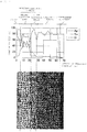
- FIG. 4 is a diagram showing a correspondence relationship between a graph of concentration distribution of elements and the mapping diagram of the elements in the stretchable mounting board of Example 1.
- FIG. 5 is a diagram focusing on tin in the mapping diagram in FIG. 4 .
- FIG. 6 is a diagram focusing on bismuth in the mapping diagram in FIG. 4 .
- the "concentration” (unit: %) indicated by a vertical axis of the graphs in FIGS. 4 , 5 , and 6 is standardized with a maximum concentration of each element being 100%.
- the stretchable mounting board of Example 1 As shown in the mapping diagram in FIG. 4 , in the stretchable mounting board of Example 1, a boundary between the stretchable wiring and the mounting electrode section was identified, and it was also confirmed that the mounting electrode section was a two-layer structure having the first electrode layer and the second electrode layer.
- mapping diagram A state where tin in the solder diffused in the second electrode layer and the first electrode layer sequentially was confirmed from the mapping diagram (focusing on tin) in FIG. 5 . Further, a state where the bismuth in the solder diffused in the second electrode layer, but not easily diffused in the first electrode layer was confirmed from the mapping diagram in FIG. 6 (focusing on bismuth). In the mapping diagram (focusing on bismuth) in FIG. 6 , it is difficult to confirm a presence or absence of bismuth in the first electrode layer, but a presence of bismuth in the first electrode layer was confirmed as can be seen from the graph in FIG. 6 . It was also confirmed that a bismuth eutectic size in the first electrode layer was smaller than a bismuth eutectic size in the second electrode layer.
- a resistance of the stretchable wiring of the stretchable mounting boards of Example 1 and Comparative Example 1 was measured while changing an expansion ratio. For the measurement, a plurality of the stretchable mounting boards of Example 1 and a plurality of the stretchable mounting boards of Comparative Example 1 were used.
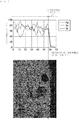
- FIG. 7 is a graph showing a relationship between the expansion ratio and the resistance of stretchable wiring of the stretchable mounting boards of Example 1 and Comparative Example 1.
- an increase in the resistance of the stretchable wiring due to the expansion of the stretchable mounting board was suppressed in the stretchable mounting board of Example 1 more than in the stretchable mounting board of Comparative Example 1.
- the resistance of the stretchable wiring starts to rise sharply, which is considered to indicate that the stretchable wiring starts to be disconnected.
- a disconnection of the stretchable wiring during the expansion of the stretchable mounting board was suppressed in the stretchable mounting board of Example 1 more than in the stretchable mounting board of Comparative Example 1.
- the stretchable mounting board of Example 1 could expand to about 40%, whereas the stretchable mounting board of Comparative Example 1 could expand up to only about 20%.
- the stretchable wiring and the solder reacted with each other to generate a brittle metal compound including bismuth.
- a cross section of the stretchable mounting board of Comparative Example 2 was exposed by polishing, and then mapping of each element was performed using the scanning electron microscope-energy dispersive X-ray spectroscopy (SEM-EDS). Subsequently, a concentration distribution of each element was obtained by cross-section profiling in a thickness direction with respect to the obtained mapping diagram of each element.
- SEM-EDS scanning electron microscope-energy dispersive X-ray spectroscopy
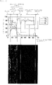
- FIG. 8 is a diagram showing a correspondence relationship between a graph of concentration distribution of elements and the mapping diagram of the elements in the stretchable mounting board of Comparative Example 2.
- FIG. 9 is a diagram focusing on tin in the mapping diagram in FIG. 8 .
- FIG. 10 is a diagram focusing on bismuth in the mapping diagram in FIG. 8 .
- the "concentration” (unit: %) indicated by a vertical axis of the graphs in FIGS. 8 , 9 , and 10 is standardized with a maximum concentration of each element being 100%.
- “A distance in the thickness direction” (unit: ⁇ m) indicated by a horizontal axis of the graphs in FIGS.
- mapping diagram focusing on tin
- FIG. 10 It was confirmed from the mapping diagram (focusing on bismuth) in FIG. 9 that tin in the solder diffused in the mounting electrode section and the stretchable wiring. Further, a state in which bismuth in the solder diffused in the mounting electrode section and the stretchable wiring was confirmed from the mapping diagram (focusing on bismuth) in FIG. 10 .
- a resistance of the stretchable wiring of the stretchable mounting boards of Comparative Example 2 was measured while changing an expansion ratio. For the measurement, a plurality of the stretchable mounting boards of Comparative Example 2 was used.
- FIG. 11 is a graph showing a relationship between the expansion ratio and the resistance of the stretchable wiring in the stretchable mounting board of Comparative Example 2. Comparing FIGS. 7 and 11 , a disconnection of the stretchable wiring when the stretchable mounting board expanded and contracted was not suppressed in the stretchable mounting board of Comparative Example 2 more than in the stretchable mounting board of Example 1. More specifically, as a range of the expansion ratio in which the stretchable wiring is not considered to be disconnected, the stretchable mounting board of Example 1 could expand to about 40%, whereas the stretchable mounting board of Comparative Example 2 could expand up to only about 15%.
Landscapes
- Engineering & Computer Science (AREA)
- Microelectronics & Electronic Packaging (AREA)
- Life Sciences & Earth Sciences (AREA)
- Manufacturing & Machinery (AREA)
- Health & Medical Sciences (AREA)
- Medical Informatics (AREA)
- Surgery (AREA)
- Pathology (AREA)
- Biomedical Technology (AREA)
- Heart & Thoracic Surgery (AREA)
- Physics & Mathematics (AREA)
- Molecular Biology (AREA)
- Biophysics (AREA)
- Animal Behavior & Ethology (AREA)
- General Health & Medical Sciences (AREA)
- Public Health (AREA)
- Veterinary Medicine (AREA)
- Electric Connection Of Electric Components To Printed Circuits (AREA)
- Parts Printed On Printed Circuit Boards (AREA)
- Measurement And Recording Of Electrical Phenomena And Electrical Characteristics Of The Living Body (AREA)
- Structure Of Printed Boards (AREA)
Abstract
Description
- The present invention relates to a stretchable mounting board.
- In recent years, a wiring board has been used to manage a state and the like of a living body (for example, a human body) by acquiring and analyzing biological information.
- An electronic component may be mounted on such a wiring board. For example,
Patent Document 1 discloses a mounting board in which an electronic component is mounted on an insulating substrate with solder and a conductor interposed therebetween. - Patent Document 1: International Publication No.
2009/081929 - A mounting board in which an electronic component is mounted on a wiring board is required to have stretchability capable of following a movement of a living body when attached to the living body. As a constituent material of wiring of the mounting board having such stretchability, for example, a mixture of conductive particles and a resin is used. When the electronic component is connected to such wiring with solder interposed therebetween, the wiring and the solder may react with each other to generate a brittle metal compound. Therefore, when the mounting board expands or contracts, the wiring is likely to be disconnected with a region where the brittle metal compound is generated as a starting point.
-
Patent Document 1 does not disclose that the mounting board has stretchability. Further, a second conductor that is in contact with the solder is configured by a member including copper. Wettability of the solder with respect to the second conductor is insufficient, and thus an electrical and mechanical connection between the solder and the second conductor is insufficient. - The present invention has been made to solve the above problems. An object of the present invention is to provide a stretchable mounting board that can suppress a disconnection of stretchable wiring during expansion and contraction when an electronic component is connected to the stretchable wiring with solder interposed therebetween, while ensuring an electrical and mechanical connection.
- A stretchable mounting board of the present invention includes a stretchable substrate, a stretchable wiring disposed on one main surface of the stretchable substrate, a mounting electrode section connected to the stretchable wiring and including bismuth and tin, solder connected to the mounting electrode section and including bismuth and tin, and an electronic component connected to the mounting electrode section with the solder interposed therebetween, in which the mounting electrode section has a first electrode layer on a side of the stretchable wiring and a second electrode layer on a side of the solder, and a concentration of bismuth in the first electrode layer is lower than a concentration of bismuth in the second electrode layer and is constant along a thickness direction.
- Provided in the present invention is a stretchable mounting board which can suppress a disconnection of stretchable wiring during expansion and contraction when an electronic component is connected to the stretchable wiring with solder interposed therebetween, while ensuring an electrical and mechanical connection.
-
-
FIG. 1 is a schematic sectional view showing one example of a stretchable mounting board of the present invention. -
FIG. 2 is a schematic sectional view showing another example of the stretchable mounting board of the present invention. -
FIG. 3 is a schematic sectional view showing still another example of the stretchable mounting board of the present invention. -
FIG. 4 is a diagram showing a correspondence relationship between a graph of concentration distribution of elements and a mapping diagram of the elements in the stretchable mounting board of Example 1. -
FIG. 5 is a diagram focusing on tin in the mapping diagram inFIG. 4 . -
FIG. 6 is a diagram focusing on bismuth in the mapping diagram inFIG. 4 . -
FIG. 7 is a graph showing a relationship between an expansion ratio and a resistance of stretchable wiring of the stretchable mounting boards of Example 1 and Comparative Example 1. -
FIG. 8 is a diagram showing a correspondence relationship between a graph of concentration distribution of elements and a mapping diagram of the elements in a stretchable mounting board of Comparative Example 2. -
FIG. 9 is a diagram focusing on tin in the mapping diagram inFIG. 8 . -
FIG. 10 is a diagram focusing on bismuth in the mapping diagram inFIG. 8 . -
FIG. 11 is a graph showing a relationship between an expansion ratio and a resistance of the stretchable wiring in a stretchable mounting board of Comparative Example 2. - A stretchable mounting board of the present invention will be described below. The present invention is not limited to the following configurations, and may be modified as appropriate without departing from the gist of the present invention. Further, a combination of a plurality of individual preferable configurations described below is also the present invention.
- In the present specification, a "thickness" means a length in a direction perpendicular to a surface of the stretchable substrate in a sectional view. Further, the "thickness" is indicated as in a state where the stretchable mounting board is not stretched unless otherwise specified.
-
FIG. 1 is a schematic sectional view showing one example of a stretchable mounting board of the present invention. As shown inFIG. 1 , thestretchable mounting board 1 has astretchable substrate 10,stretchable wiring 20, amounting electrode section 30,solder 40, and anelectronic component 50. - The
stretchable substrate 10 preferably includes at least one resin selected from the group consisting of a silicone resin, an acrylic resin, an olefin resin, and a urethane resin. Examples of the urethane resins include thermoplastic polyurethane. - When the
stretchable mounting board 1 is attached to a living body, a thickness of thestretchable substrate 10 is preferably 100 µm or less, and more preferably 50 µm or less, so as not to inhibit expansion and contraction of a surface of the living body. Further, the thickness of thestretchable substrate 10 is preferably 10 µm or more. - The
stretchable wiring 20 is disposed on one main surface of thestretchable substrate 10. - Examples of constituent materials of the
stretchable wiring 20 include a mixture of conductive particles and a resin. Above all, thestretchable wiring 20 preferably includes silver as conductive particles and a resin. - In addition to silver, examples of the conductive particles include copper and nickel. An average particle diameter of the conductive particles is preferably 0.01 µm or more and 10 µm or less. A shape of the conductive particles is preferably spherical.
- The resin preferably includes at least one resin (elastomer resin) selected from the group consisting of an epoxy resin, a urethane resin, an acrylic resin, and a silicone resin.
- A thickness of the
stretchable wiring 20 is preferably 100 µm or less, and more preferably 50 µm or less. Further, the thickness of thestretchable wiring 20 is preferably 1 µm or more. - The
mounting electrode section 30 is connected to thestretchable wiring 20. More specifically, themounting electrode section 30 is in contact with a side of thestretchable wiring 20 opposite to thestretchable substrate 10. - The
mounting electrode section 30 includes silver, bismuth, tin, and a resin. Themounting electrode section 30 may include another metal such as copper, aluminum, or nickel in addition to silver, bismuth, and tin. Themounting electrode section 30 may include a metal such as copper, aluminum, or nickel instead of silver. For example, themounting electrode section 30 may include copper, bismuth, tin, or a resin. As the resin included in the mountingelectrode section 30, a resin (elastomer resin) such as an epoxy resin, a urethane resin, an acrylic resin, a silicone resin, a polyester resin, or the like can be used. - The mounting
electrode section 30 has afirst electrode layer 31 on a side of thestretchable wiring 20 and asecond electrode layer 32 on a side of thesolder 40. - A concentration of the bismuth in the
first electrode layer 31 is lower than a concentration of the bismuth in thesecond electrode layer 32, and is constant along a thickness direction. It can be said that in the mountingelectrode section 30, bismuth is densely distributed in thesecond electrode layer 32, but is not densely distributed in thefirst electrode layer 31 as a whole. - In the
stretchable mounting board 1, although thesolder 40 includes bismuth, thesecond electrode layer 32 in which bismuth is densely distributed is disposed on the side of thesolder 40 in the mountingelectrode section 30 as will be described later. Thus, wettability of thesolder 40 with respect to thesecond electrode layer 32 is good, and an electrical and mechanical connection between thesecond electrode layer 32 and thesolder 40 is secured. - Here, in a conventional stretchable mounting board that does not have the mounting
electrode section 30, when thestretchable wiring 20 includes a mixture of conductive particles and a resin, thestretchable wiring 20 reacts with thesolder 40 to generate a brittle metal compound which will be a starting point of disconnection of thestretchable wiring 20 during expansion and contraction. As will be described later, thesolder 40 includes bismuth, and this brittle metal compound includes bismuth diffused from thesolder 40. - On the other hand, in the
stretchable mounting board 1, thefirst electrode layer 31 in which bismuth is not densely distributed in the mountingelectrode section 30 is disposed on the side of thestretchable wiring 20. Thus, a brittle metal compound as in the conventional stretchable mounting board is not generated, and a disconnection of thestretchable wiring 20 is suppressed when thestretchable mounting board 1 expands and contracts. - The concentration of bismuth in the
first electrode layer 31 and thesecond electrode layer 32 is determined from a concentration distribution obtained by cross-section profiling in the thickness direction with respect to the mapping diagram of each element by a scanning electron microscope-energy dispersive X-ray spectroscopy (SEM-EDS). "The concentration is constant along a thickness direction" described herein means that a rate of change of the concentration is within ± 5% over a range of 5 µm or more along the thickness direction. - A bismuth eutectic size in the
second electrode layer 32 is preferably larger than a bismuth eutectic size in thefirst electrode layer 31. In this case, it can be said that the concentration of bismuth in thefirst electrode layer 31 is considerably lower than the concentration of bismuth in thesecond electrode layer 32. Thus, the electrical and mechanical connection between thesecond electrode layer 32 and thesolder 40 is sufficiently ensured. Further, an action of thefirst electrode layer 31 sufficiently suppresses a disconnection of thestretchable wiring 20 when thestretchable mounting board 1 expands and contracts. - The bismuth eutectic size in the
second electrode layer 32 is preferably 1 µm or more. - The bismuth eutectic size in the
first electrode layer 31 and the bismuth eutectic size in thesecond electrode layer 32 are determined as follows. First, the cross-sections of thefirst electrode layer 31 and thesecond electrode layer 32 of thestretchable mounting board 1 are exposed by polishing. Then, bismuth-rich eutectic parts in the electrode layers are binarized using image analysis software, and then an area is determined, and an equivalent circle diameter is calculated. This circle equivalent diameter is determined as a particle diameter of the bismuth eutectic part. As the image analysis software, "Photoshop" manufactured by Adobe Systems Incorporated is used. Then, distribution of the particle diameter is calculated, and a particle diameter at a frequency of 50% is determined as an average particle diameter. The average particle diameter thus obtained in each electrode layer is determined as the bismuth eutectic size. - A concentration of the tin in the
first electrode layer 31 is preferably lower than the concentration of the tin in thesecond electrode layer 32. - A thickness of the
first electrode layer 31 is preferably 5 µm or more, and more preferably 10 µm or more. In this case, thesecond electrode layer 32 in which the bismuth is densely distributed and thestretchable wiring 20 are sufficiently apart from each other, and therefore a disconnection of thestretchable wiring 20 is sufficiently suppressed when thestretchable mounting board 1 expands and contracts. The thickness of thefirst electrode layer 31 of 5 µm or more suggests that thefirst electrode layer 31 has been formed by a screen printing method, an inkjet method, a dispenser method, or the like. The thickness of thefirst electrode layer 31 is preferably 40 µm or less, and more preferably 30 µm or less. - A thickness of the
second electrode layer 32 is preferably 5 µm or more. In this case, an electrical and mechanical connection between thesecond electrode layer 32 and thesolder 40 is sufficiently ensured. The thickness of thesecond electrode layer 32 of 5 µm or more suggests that thesecond electrode layer 32 has been formed by the screen printing method, the inkjet method, the dispenser method, or the like. The thickness of thesecond electrode layer 32 is preferably 20 µm or less, and more preferably 10 µm or less. - The thickness of the
first electrode layer 31 and the thickness of thesecond electrode layer 32 may be the same or different. -
FIG. 2 is a schematic sectional view showing another example of the stretchable mounting board of the present invention. As in a stretchable mountingboard 2 shown inFIG. 2 , the length of thefirst electrode layer 31 may be larger than a length of thesecond electrode layer 32 in a direction parallel to the surface of thestretchable substrate 10. In this case, thesecond electrode layer 32 in which the bismuth is densely distributed and thestretchable wiring 20 are sufficiently apart from each other with thefirst electrode layer 31 interposed therebetween. A disconnection of thestretchable wiring 20 is therefore sufficiently suppressed when thestretchable mounting board 2 expands and contracts. -
FIG. 3 is a schematic sectional view showing still another example of the stretchable mounting board of the present invention. As in a stretchable mountingboard 3 shown inFIG. 3 , the length of the mountingelectrode section 30 may be larger than a length of a part of thesolder 40 that is connected to the mountingelectrode section 30 in the direction parallel to the surface of thestretchable substrate 10. In this case, it is possible to prevent thestretchable wiring 20 and thesolder 40 from reacting with each other to generate a brittle metal compound which will be a starting point of a disconnection of thestretchable wiring 20 during expansion and contraction. - The
solder 40 is connected to the mountingelectrode section 30. More specifically, thesolder 40 is in contact with a side of the mounting electrode section 30 (second electrode layer 32) opposite to thestretchable wiring 20. - The
solder 40 includes bismuth and tin and is also referred to as a so-called low temperature solder. Thus, when thesolder 40 is used, soldering can be performed without damaging theelectronic component 50, thestretchable substrate 10 including a resin, and thestretchable wiring 20. - The
electronic component 50 is connected to the mountingelectrode section 30 with thesolder 40 interposed therebetween. - Examples of the
electronic component 50 include an amplifier (operation amplifier, transistor, and the like), a diode, an integrated circuit (IC), a capacitor, a resistor, and an inductor. - The
stretchable mounting board 1 may have an electrode connected to thestretchable wiring 20 at a position different from the mountingelectrode section 30. Thestretchable mounting board 1 can be used as a sensor by being attached to a living body with an electrode interposed therebetween. - The electrode is preferably a gel electrode. Interposing the gel electrode allows the
stretchable mounting board 1 to be attached to the living body. The gel electrode is configured by a conductive gel material including, for example, water, alcohol, a moisturizer, and an electrolyte. Examples of such gel material include hydrogel. - The
stretchable mounting board 1 is manufactured as follows, for example. - A conductive paste for stretchable wiring (for example, a conductive paste including a mixture of silver and a resin) is printed on the one main surface of the
stretchable substrate 10 by using the screen printing method or the like. Then, thestretchable wiring 20 is formed by thermosetting the conductive paste for stretchable wiring so as to obtain a predetermined resistance value. - A conductive paste for the first electrode layer (for example, a conductive paste including a mixture of silver and a resin) is printed on the side of the
stretchable wiring 20 opposite to thestretchable substrate 10 by using the screen printing method or the like. A solvent concentration of the conductive paste for the first electrode layer is, for example, 6% by weight or less. Then, thefirst electrode layer 31 is formed by thermosetting the conductive paste for the first electrode layer. - Next, a conductive paste for the second electrode layer (for example, a conductive paste including a mixture of silver and a resin) having a solvent concentration higher than the solvent concentration of the conductive paste for the first electrode layer is printed on a side of the
first electrode layer 31 opposite to thestretchable wiring 20 by using the screen printing method or the like. The solvent concentration of the conductive paste for the second electrode layer is, for example, 10% by weight or more. Then, thesecond electrode layer 32 is formed by thermosetting the conductive paste for the second electrode layer. - Examples of the solvent in the conductive paste for the first electrode layer and the conductive paste for the second electrode layer include terpineol.
- The mounting
electrode section 30 configured by thefirst electrode layer 31 and thesecond electrode layer 32 is formed as described above. Thefirst electrode layer 31 has a denser structure than thesecond electrode layer 32 due to a difference in the solvent concentration of the used conductive paste. - The
solder 40 is printed on the side of the mounting electrode section 30 (second electrode layer 32) opposite to thestretchable wiring 20 by using a metal mask or the like. Subsequently, theelectronic component 50 is mounted on thesolder 40, and then is heated in a reflow furnace. As described above, theelectronic component 50 is connected to the mountingelectrode section 30 with thesolder 40 interposed therebetween. - By being heated in the reflow furnace, the bismuth and tin in the
solder 40 diffuse (permeate) in thesecond electrode layer 32 of the mountingelectrode section 30. This is related to the fact that thesecond electrode layer 32 does not have a dense structure. Therefore, the wettability of thesolder 40 with respect to thesecond electrode layer 32 becomes good, and the electrical and mechanical connection between thesecond electrode layer 32 and thesolder 40 is secured. - On the other hand, of the bismuth and tin diffused in the
second electrode layer 32, tin having a high diffusion rate diffuses to some extent in thefirst electrode layer 31, but bismuth having a slow diffusion rate does not easily diffuse in thefirst electrode layer 31. The reason for the bismuth not to easily diffuse in thefirst electrode layer 31 has something to do with thefirst electrode layer 31 having a dense structure. - In the conventional stretchable mounting board that does not have the mounting
electrode section 30, when thestretchable wiring 20 includes a mixture of conductive particles and a resin, heat treatment in a reflow furnace during mounting of theelectronic component 50 causes a reaction between thestretchable wiring 20 and thesolder 40 to generate a brittle metal compound which will be a starting point of a disconnection of thestretchable wiring 20 during expansion and contraction. This brittle metal compound includes bismuth diffused from thesolder 40. - On the other hand, in the
stretchable mounting board 1, thefirst electrode layer 31 suppresses the diffusion of bismuth from thesolder 40 to thestretchable wiring 20. Thus, a conventional brittle metal compound is not generated, and a disconnection of thestretchable wiring 20 is suppressed when thestretchable mounting board 1 expands and contracts. - Hereinafter, examples more specifically disclosing the stretchable mounting board of the present invention will be described. Note that the present invention is not limited to only these examples.
- A stretchable mounting board of Example 1 was manufactured as follows.
- A conductive paste for stretchable wiring including a mixture of silver and a urethane resin was printed on one main surface of a stretchable substrate including thermoplastic polyurethane by a screen printing method. After that, a stretchable wiring was formed by thermosetting the printed conductive paste.
- A conductive paste for a first electrode layer including a mixture of silver and a polyester resin and having a solvent concentration of 6% by weight was printed on a side of the stretchable wiring opposite to the stretchable substrate by using the screen printing method. Terpineol was used as a solvent in the conductive paste for the first electrode layer. Then, the first electrode layer was formed by thermosetting the conductive paste for the first electrode layer.
- Next, a conductive paste for a second electrode layer including a mixture of silver and a polyester resin and having a solvent concentration of 10% by weight was printed on a side of the stretchable wiring opposite to the first electrode layer by using the screen printing method. Terpineol was used as the solvent in the conductive paste for the second electrode layer. Then, the second electrode layer was formed by thermosetting the conductive paste for the second electrode layer.
- As described above, a mounting electrode section configured by the first electrode layer and the second electrode layer was formed.
- Solder including bismuth and tin was printed on a side of the mounting electrode section (second electrode layer) opposite to the stretchable wiring by using a metal mask. Subsequently, an electronic component was mounted on the solder, and then was heated in a reflow furnace. As described above, the electronic component was connected to the mounting electrode section with the solder interposed therebetween.
- As described above, the stretchable mounting board of Example 1 was completed.
- A stretchable mounting board of Comparative Example 1 was manufactured in a similar manner to the stretchable mounting board of Example 1 except that the mounting electrode section was not formed.
- A stretchable mounting board of Comparative Example 2 was manufactured in a similar manner to the stretchable mounting board of Example 1 except that the solvent concentration in the conductive paste for the first electrode layer was 10% by weight. That is, in the stretchable mounting board of Comparative Example 2, the mounting electrode section had a one-layer structure instead of a two-layer structure.
- A cross section of the stretchable mounting board of Example 1 was exposed by polishing, and then mapping of each element was performed using a scanning electron microscope-energy dispersive X-ray spectroscopy (SEM-EDS). Subsequently, a concentration distribution of each element was obtained by cross-section profiling in a thickness direction with respect to the obtained mapping diagram of each element.
-
FIG. 4 is a diagram showing a correspondence relationship between a graph of concentration distribution of elements and the mapping diagram of the elements in the stretchable mounting board of Example 1.FIG. 5 is a diagram focusing on tin in the mapping diagram inFIG. 4 .FIG. 6 is a diagram focusing on bismuth in the mapping diagram inFIG. 4 . The "concentration" (unit: %) indicated by a vertical axis of the graphs inFIGS. 4 ,5 , and6 is standardized with a maximum concentration of each element being 100%. "A distance in the thickness direction" (unit: µm) indicated by a horizontal axis of the graphs inFIGS. 4 ,5 , and6 is a thickness direction from a vicinity of an interface between the solder and the mounting electrode section toward the stretchable substrate. Note that, in the graphs inFIGS. 4 ,5 , and6 , the concentration distribution of silver (Ag), tin (Sn), and bismuth (Bi) is shown as a representative among the elements configuring the stretchable mounting board of Example 1. - As shown in the mapping diagram in
FIG. 4 , in the stretchable mounting board of Example 1, a boundary between the stretchable wiring and the mounting electrode section was identified, and it was also confirmed that the mounting electrode section was a two-layer structure having the first electrode layer and the second electrode layer. - As shown in the graph in
FIG. 4 , bismuth and tin in the solder diffused in the second electrode layer in the stretchable mounting board of Example 1. It was therefore observed that wettability of the solder with respect to the second electrode layer became good, and an electrical and mechanical connection between the second electrode layer and the solder was secured. On the other hand, although diffusion of tin was observed from the second electrode layer to the first electrode layer, diffusion of bismuth was suppressed. As a result, the concentration of the bismuth in the first electrode layer was lower than the concentration of the bismuth in the second electrode layer, and was constant along the thickness direction. Further, diffusion of both tin and bismuth from the first electrode layer to the stretchable wiring was suppressed. - A state where tin in the solder diffused in the second electrode layer and the first electrode layer sequentially was confirmed from the mapping diagram (focusing on tin) in
FIG. 5 . Further, a state where the bismuth in the solder diffused in the second electrode layer, but not easily diffused in the first electrode layer was confirmed from the mapping diagram inFIG. 6 (focusing on bismuth). In the mapping diagram (focusing on bismuth) inFIG. 6 , it is difficult to confirm a presence or absence of bismuth in the first electrode layer, but a presence of bismuth in the first electrode layer was confirmed as can be seen from the graph inFIG. 6 . It was also confirmed that a bismuth eutectic size in the first electrode layer was smaller than a bismuth eutectic size in the second electrode layer. - A resistance of the stretchable wiring of the stretchable mounting boards of Example 1 and Comparative Example 1 was measured while changing an expansion ratio. For the measurement, a plurality of the stretchable mounting boards of Example 1 and a plurality of the stretchable mounting boards of Comparative Example 1 were used.
-
FIG. 7 is a graph showing a relationship between the expansion ratio and the resistance of stretchable wiring of the stretchable mounting boards of Example 1 and Comparative Example 1. As shown inFIG. 7 , an increase in the resistance of the stretchable wiring due to the expansion of the stretchable mounting board was suppressed in the stretchable mounting board of Example 1 more than in the stretchable mounting board of Comparative Example 1. Further, the resistance of the stretchable wiring starts to rise sharply, which is considered to indicate that the stretchable wiring starts to be disconnected. However, a disconnection of the stretchable wiring during the expansion of the stretchable mounting board was suppressed in the stretchable mounting board of Example 1 more than in the stretchable mounting board of Comparative Example 1. More specifically, as a range of the expansion ratio in which the stretchable wiring is not considered to be disconnected, the stretchable mounting board of Example 1 could expand to about 40%, whereas the stretchable mounting board of Comparative Example 1 could expand up to only about 20%. As a result of actual observation, in the stretchable mounting board of Comparative Example 1, the stretchable wiring and the solder reacted with each other to generate a brittle metal compound including bismuth. - A cross section of the stretchable mounting board of Comparative Example 2 was exposed by polishing, and then mapping of each element was performed using the scanning electron microscope-energy dispersive X-ray spectroscopy (SEM-EDS). Subsequently, a concentration distribution of each element was obtained by cross-section profiling in a thickness direction with respect to the obtained mapping diagram of each element.
-
FIG. 8 is a diagram showing a correspondence relationship between a graph of concentration distribution of elements and the mapping diagram of the elements in the stretchable mounting board of Comparative Example 2.FIG. 9 is a diagram focusing on tin in the mapping diagram inFIG. 8 .FIG. 10 is a diagram focusing on bismuth in the mapping diagram inFIG. 8 . The "concentration" (unit: %) indicated by a vertical axis of the graphs inFIGS. 8 ,9 , and10 is standardized with a maximum concentration of each element being 100%. "A distance in the thickness direction" (unit: µm) indicated by a horizontal axis of the graphs inFIGS. 8 ,9 , and10 is a thickness direction from a vicinity of an interface between the solder and the mounting electrode section toward the stretchable substrate. Note that, in the graphs inFIGS. 8 ,9 , and10 , the concentration distribution of silver (Ag), tin (Sn), and bismuth (Bi) is shown as a representative among the elements configuring the stretchable mounting board of Comparative Example 2. - As shown in the mapping diagram in
FIG. 8 , in the stretchable mounting board of Comparative Example 2, a boundary between the stretchable substrate and the stretchable wiring was determined, but a boundary between the stretchable wiring and the mounting electrode section was not determined. - As shown in the graph in
FIG. 8 , in the stretchable mounting board of Comparative Example 2, bismuth and tin in the solder diffused through the mounting electrode section into the stretchable wiring. That is, in the stretchable mounting board of Comparative Example 2, the diffusion of tin and bismuth could not be controlled by the mounting electrode section. - It was confirmed from the mapping diagram (focusing on tin) in
FIG. 9 that tin in the solder diffused in the mounting electrode section and the stretchable wiring. Further, a state in which bismuth in the solder diffused in the mounting electrode section and the stretchable wiring was confirmed from the mapping diagram (focusing on bismuth) inFIG. 10 . - A resistance of the stretchable wiring of the stretchable mounting boards of Comparative Example 2 was measured while changing an expansion ratio. For the measurement, a plurality of the stretchable mounting boards of Comparative Example 2 was used.
-
FIG. 11 is a graph showing a relationship between the expansion ratio and the resistance of the stretchable wiring in the stretchable mounting board of Comparative Example 2. ComparingFIGS. 7 and11 , a disconnection of the stretchable wiring when the stretchable mounting board expanded and contracted was not suppressed in the stretchable mounting board of Comparative Example 2 more than in the stretchable mounting board of Example 1. More specifically, as a range of the expansion ratio in which the stretchable wiring is not considered to be disconnected, the stretchable mounting board of Example 1 could expand to about 40%, whereas the stretchable mounting board of Comparative Example 2 could expand up to only about 15%. -
- 1,2,3:
- Stretchable mounting board
- 10:
- Stretchable substrate
- 20:
- Stretchable wiring
- 30:
- Mounting electrode section
- 31:
- First electrode layer
- 32:
- Second electrode layer
- 40:
- Solder
- 50:
- Electronic component
Claims (8)
- A stretchable mounting board comprising:a stretchable substrate;a stretchable wiring disposed on one main surface of the stretchable substrate;a mounting electrode section connected to the stretchable wiring and including bismuth and tin;solder connected to the mounting electrode section and including bismuth and tin; andan electronic component connected to the mounting electrode section with the solder interposed between the electronic component and the mounting electrode,
whereinthe mounting electrode section has a first electrode layer on a side of the stretchable wiring and a second electrode layer on a side of the solder, anda concentration of bismuth in the first electrode layer is lower than a concentration of bismuth in the second electrode layer and is constant along a thickness direction. - The stretchable mounting board according to claim 1, wherein a bismuth eutectic size in the second electrode layer is larger than a bismuth eutectic size in the first electrode layer.
- The stretchable mounting board according to claim 2, wherein the bismuth eutectic size in the second electrode layer is 1 µm or more.
- The stretchable mounting board according to any one of claims 1 to 3, wherein the first electrode layer has a thickness of 5 µm or more.
- The stretchable mounting board according to any one of claims 1 to 4, wherein the second electrode layer has a thickness of 5 µm or more.
- The stretchable mounting board according to any one of claims 1 to 5, wherein the stretchable wiring includes silver and a resin.
- The stretchable mounting board according to claim 6, wherein the resin includes at least one resin selected from the group consisting of an epoxy resin, a urethane resin, an acrylic resin, and a silicone resin.
- The stretchable mounting board according to any one of claims 1 to 7, wherein the stretchable substrate includes at least one resin selected from the group consisting of a silicone resin, an acrylic resin, an olefin resin, and a urethane resin.
Applications Claiming Priority (2)
| Application Number | Priority Date | Filing Date | Title |
|---|---|---|---|
| JP2019067973 | 2019-03-29 | ||
| PCT/JP2020/010718 WO2020203135A1 (en) | 2019-03-29 | 2020-03-12 | Stretchable mounting substrate |
Publications (2)
| Publication Number | Publication Date |
|---|---|
| EP3785620A1 true EP3785620A1 (en) | 2021-03-03 |
| EP3785620A4 EP3785620A4 (en) | 2022-03-23 |
Family
ID=72668715
Family Applications (1)
| Application Number | Title | Priority Date | Filing Date |
|---|---|---|---|
| EP20782678.5A Pending EP3785620A4 (en) | 2019-03-29 | 2020-03-12 | STRETCHABLE MOUNTING SUBSTRATE |
Country Status (5)
| Country | Link |
|---|---|
| US (2) | US11212915B2 (en) |
| EP (1) | EP3785620A4 (en) |
| JP (1) | JP6962478B2 (en) |
| CN (1) | CN112384141B (en) |
| WO (1) | WO2020203135A1 (en) |
Families Citing this family (3)
| Publication number | Priority date | Publication date | Assignee | Title |
|---|---|---|---|---|
| WO2020203135A1 (en) * | 2019-03-29 | 2020-10-08 | 株式会社村田製作所 | Stretchable mounting substrate |
| CN114846911B (en) | 2020-09-29 | 2025-06-03 | 株式会社村田制作所 | Stretchable mounting substrate and method for manufacturing stretchable mounting substrate |
| EP4412403A4 (en) * | 2021-12-08 | 2025-10-01 | Murata Manufacturing Co | EXPANDABLE DEVICE |
Family Cites Families (18)
| Publication number | Priority date | Publication date | Assignee | Title |
|---|---|---|---|---|
| US3039760A (en) | 1960-08-30 | 1962-06-19 | Gen Motors Corp | Shock absorber and air spring unit assembly |
| JPH09260822A (en) * | 1996-03-18 | 1997-10-03 | Teikoku Tsushin Kogyo Co Ltd | Electronic component connection fixing structure by soldering to the board |
| JP2001184949A (en) * | 1999-12-24 | 2001-07-06 | Asahi Kasei Corp | Anisotropic conductive material |
| JP3779864B2 (en) * | 2000-07-19 | 2006-05-31 | 古河電気工業株式会社 | Electronic component lead wire, method for manufacturing the same, and electronic component using the lead wire |
| KR100705637B1 (en) * | 2002-07-03 | 2007-04-10 | 미츠이 긴조쿠 고교 가부시키가이샤 | Flexible wiring base material and its manufacturing method |
| TWI243462B (en) * | 2004-05-14 | 2005-11-11 | Advanced Semiconductor Eng | Semiconductor package including passive component |
| JP2007300038A (en) * | 2006-05-08 | 2007-11-15 | Matsushita Electric Ind Co Ltd | Electronic component mounting body and manufacturing method thereof |
| JP5220766B2 (en) | 2007-12-26 | 2013-06-26 | 株式会社フジクラ | Mounting board |
| JP6182877B2 (en) * | 2013-01-28 | 2017-08-23 | 富士通株式会社 | Solder paste, conductive adhesive, manufacturing method thereof, and manufacturing method of semiconductor device |
| JP6187226B2 (en) * | 2013-12-16 | 2017-08-30 | 富士通株式会社 | Manufacturing method of electronic device |
| JP6287310B2 (en) * | 2014-02-18 | 2018-03-07 | 富士通株式会社 | Electronic component, method for manufacturing electronic component, and method for manufacturing electronic device |
| CN107205677B (en) * | 2015-01-14 | 2020-12-25 | 东洋纺株式会社 | Stretchable electrode sheet and contact surface for measuring biological information |
| JP6518451B2 (en) * | 2015-02-02 | 2019-05-22 | 株式会社フジクラ | Elastic circuit board |
| JP6574576B2 (en) * | 2015-02-02 | 2019-09-11 | 株式会社フジクラ | Elastic wiring board |
| JP6439472B2 (en) * | 2015-02-06 | 2018-12-19 | 富士通株式会社 | Electronic device and method of manufacturing electronic device |
| JP2018014381A (en) * | 2016-07-20 | 2018-01-25 | 富士通株式会社 | Substrate and electronic equipment |
| JP6967726B2 (en) * | 2018-01-31 | 2021-11-17 | パナソニックIpマネジメント株式会社 | Solder paste and mounting structure |
| WO2020203135A1 (en) * | 2019-03-29 | 2020-10-08 | 株式会社村田製作所 | Stretchable mounting substrate |
-
2020
- 2020-03-12 WO PCT/JP2020/010718 patent/WO2020203135A1/en not_active Ceased
- 2020-03-12 JP JP2020542036A patent/JP6962478B2/en active Active
- 2020-03-12 CN CN202080003919.XA patent/CN112384141B/en active Active
- 2020-03-12 EP EP20782678.5A patent/EP3785620A4/en active Pending
- 2020-10-14 US US17/070,499 patent/US11212915B2/en active Active
-
2021
- 2021-11-16 US US17/527,412 patent/US11653445B2/en active Active
Also Published As
| Publication number | Publication date |
|---|---|
| EP3785620A4 (en) | 2022-03-23 |
| US20210045236A1 (en) | 2021-02-11 |
| US11212915B2 (en) | 2021-12-28 |
| CN112384141A (en) | 2021-02-19 |
| JPWO2020203135A1 (en) | 2021-04-30 |
| CN112384141B (en) | 2024-08-16 |
| US20220078904A1 (en) | 2022-03-10 |
| WO2020203135A1 (en) | 2020-10-08 |
| JP6962478B2 (en) | 2021-11-05 |
| US11653445B2 (en) | 2023-05-16 |
Similar Documents
| Publication | Publication Date | Title |
|---|---|---|
| US11653445B2 (en) | Stretchable mounting board | |
| DE102015102866B4 (en) | Ceramic component, component arrangement and method for producing a ceramic component | |
| DE19930308B4 (en) | Multichip module with silicon carrier substrate | |
| US6816385B1 (en) | Compliant laminate connector | |
| DE102011056515B4 (en) | Electrical component and method for producing an electrical component | |
| EP2234466B1 (en) | Mounting board and method of producing the same | |
| US8466374B2 (en) | Base for circuit board, circuit board, and method of fabricating thereof | |
| DE102007031966A1 (en) | Structure of an image sensor module and manufacturing method for a wafer level package | |
| US20090085216A1 (en) | Semiconductor device | |
| US9686860B2 (en) | Printed circuit board and method of fabricating the same | |
| US10186479B2 (en) | Semiconductor device, package, and vehicle | |
| DE102014111533A1 (en) | chip system | |
| JP2003273280A (en) | Chip package and manufacturing method thereof | |
| EP2130222B1 (en) | A carrier for bonding a semiconductor chip onto and a method of contacting a semiconductor chip to a carrier | |
| DE102011017543B4 (en) | Electronic device and wiring board | |
| DE102008022733B4 (en) | Functional unit and method for its production | |
| DE102014101408A1 (en) | Chip arrangement and method for producing a chip arrangement | |
| US6946733B2 (en) | Ball grid array package having testing capability after mounting | |
| DE10059808A1 (en) | Method of connecting an integrated circuit and a flexible circuit | |
| JP7008529B2 (en) | Lead wires for inspection equipment, lead wire mounting parts, and inspection jigs | |
| US12035464B2 (en) | Stretchable mounting board and method for manufacturing stretchable mounting board | |
| DE102004058413B4 (en) | Method for producing a chip-size packing structure | |
| JP4563751B2 (en) | Manufacturing method of probe needle | |
| DE112016004714T5 (en) | Surface configurations for connection pads in microelectronic structures | |
| EP2778119B1 (en) | Sensor and method for the production of a flexible soldered joint between a sensor and a printed circuit board |
Legal Events
| Date | Code | Title | Description |
|---|---|---|---|
| STAA | Information on the status of an ep patent application or granted ep patent |
Free format text: STATUS: THE INTERNATIONAL PUBLICATION HAS BEEN MADE |
|
| PUAI | Public reference made under article 153(3) epc to a published international application that has entered the european phase |
Free format text: ORIGINAL CODE: 0009012 |
|
| STAA | Information on the status of an ep patent application or granted ep patent |
Free format text: STATUS: REQUEST FOR EXAMINATION WAS MADE |
|
| 17P | Request for examination filed |
Effective date: 20201127 |
|
| AK | Designated contracting states |
Kind code of ref document: A1 Designated state(s): AL AT BE BG CH CY CZ DE DK EE ES FI FR GB GR HR HU IE IS IT LI LT LU LV MC MK MT NL NO PL PT RO RS SE SI SK SM TR |
|
| AX | Request for extension of the european patent |
Extension state: BA ME |
|
| REG | Reference to a national code |
Ref country code: DE Ref legal event code: R079 Free format text: PREVIOUS MAIN CLASS: A61B0005040800 Ipc: H05K0003340000 |
|
| A4 | Supplementary search report drawn up and despatched |
Effective date: 20220217 |
|
| RIC1 | Information provided on ipc code assigned before grant |
Ipc: H05K 1/02 20060101ALI20220211BHEP Ipc: H05K 3/24 20060101ALI20220211BHEP Ipc: H05K 1/18 20060101ALI20220211BHEP Ipc: H05K 1/09 20060101ALI20220211BHEP Ipc: A61B 5/263 20210101ALI20220211BHEP Ipc: A61B 5/25 20210101ALI20220211BHEP Ipc: H05K 3/34 20060101AFI20220211BHEP |
|
| DAV | Request for validation of the european patent (deleted) | ||
| DAX | Request for extension of the european patent (deleted) | ||
| STAA | Information on the status of an ep patent application or granted ep patent |
Free format text: STATUS: EXAMINATION IS IN PROGRESS |
|
| 17Q | First examination report despatched |
Effective date: 20250220 |