EP3783801A1 - Conversion circuit - Google Patents
Conversion circuit Download PDFInfo
- Publication number
- EP3783801A1 EP3783801A1 EP19217388.8A EP19217388A EP3783801A1 EP 3783801 A1 EP3783801 A1 EP 3783801A1 EP 19217388 A EP19217388 A EP 19217388A EP 3783801 A1 EP3783801 A1 EP 3783801A1
- Authority
- EP
- European Patent Office
- Prior art keywords
- terminal
- circuit
- voltage
- main device
- electrically connected
- Prior art date
- Legal status (The legal status is an assumption and is not a legal conclusion. Google has not performed a legal analysis and makes no representation as to the accuracy of the status listed.)
- Withdrawn
Links
- 238000006243 chemical reaction Methods 0.000 title claims abstract description 33
- 238000010586 diagram Methods 0.000 description 15
- 239000004065 semiconductor Substances 0.000 description 7
- 230000010354 integration Effects 0.000 description 5
- 230000002159 abnormal effect Effects 0.000 description 4
- 239000003990 capacitor Substances 0.000 description 4
- 239000000758 substrate Substances 0.000 description 4
- JMASRVWKEDWRBT-UHFFFAOYSA-N Gallium nitride Chemical compound [Ga]#N JMASRVWKEDWRBT-UHFFFAOYSA-N 0.000 description 2
- 102100029469 WD repeat and HMG-box DNA-binding protein 1 Human genes 0.000 description 2
- 101710097421 WD repeat and HMG-box DNA-binding protein 1 Proteins 0.000 description 2
- 230000003247 decreasing effect Effects 0.000 description 2
- 230000005669 field effect Effects 0.000 description 2
- HBMJWWWQQXIZIP-UHFFFAOYSA-N silicon carbide Chemical compound [Si+]#[C-] HBMJWWWQQXIZIP-UHFFFAOYSA-N 0.000 description 2
- 229910002601 GaN Inorganic materials 0.000 description 1
- 238000000034 method Methods 0.000 description 1
- 239000013641 positive control Substances 0.000 description 1
- 238000005215 recombination Methods 0.000 description 1
- 230000006798 recombination Effects 0.000 description 1
- 229910010271 silicon carbide Inorganic materials 0.000 description 1
Images




Classifications
-
- H—ELECTRICITY
- H03—ELECTRONIC CIRCUITRY
- H03K—PULSE TECHNIQUE
- H03K17/00—Electronic switching or gating, i.e. not by contact-making and –breaking
- H03K17/08—Modifications for protecting switching circuit against overcurrent or overvoltage
- H03K17/082—Modifications for protecting switching circuit against overcurrent or overvoltage by feedback from the output to the control circuit
- H03K17/0822—Modifications for protecting switching circuit against overcurrent or overvoltage by feedback from the output to the control circuit in field-effect transistor switches
-
- H—ELECTRICITY
- H02—GENERATION; CONVERSION OR DISTRIBUTION OF ELECTRIC POWER
- H02M—APPARATUS FOR CONVERSION BETWEEN AC AND AC, BETWEEN AC AND DC, OR BETWEEN DC AND DC, AND FOR USE WITH MAINS OR SIMILAR POWER SUPPLY SYSTEMS; CONVERSION OF DC OR AC INPUT POWER INTO SURGE OUTPUT POWER; CONTROL OR REGULATION THEREOF
- H02M7/00—Conversion of AC power input into DC power output; Conversion of DC power input into AC power output
- H02M7/02—Conversion of AC power input into DC power output without possibility of reversal
- H02M7/04—Conversion of AC power input into DC power output without possibility of reversal by static converters
- H02M7/12—Conversion of AC power input into DC power output without possibility of reversal by static converters using discharge tubes with control electrode or semiconductor devices with control electrode
- H02M7/21—Conversion of AC power input into DC power output without possibility of reversal by static converters using discharge tubes with control electrode or semiconductor devices with control electrode using devices of a triode or transistor type requiring continuous application of a control signal
- H02M7/217—Conversion of AC power input into DC power output without possibility of reversal by static converters using discharge tubes with control electrode or semiconductor devices with control electrode using devices of a triode or transistor type requiring continuous application of a control signal using semiconductor devices only
-
- H—ELECTRICITY
- H02—GENERATION; CONVERSION OR DISTRIBUTION OF ELECTRIC POWER
- H02M—APPARATUS FOR CONVERSION BETWEEN AC AND AC, BETWEEN AC AND DC, OR BETWEEN DC AND DC, AND FOR USE WITH MAINS OR SIMILAR POWER SUPPLY SYSTEMS; CONVERSION OF DC OR AC INPUT POWER INTO SURGE OUTPUT POWER; CONTROL OR REGULATION THEREOF
- H02M3/00—Conversion of DC power input into DC power output
- H02M3/02—Conversion of DC power input into DC power output without intermediate conversion into AC
- H02M3/04—Conversion of DC power input into DC power output without intermediate conversion into AC by static converters
- H02M3/10—Conversion of DC power input into DC power output without intermediate conversion into AC by static converters using discharge tubes with control electrode or semiconductor devices with control electrode
- H02M3/145—Conversion of DC power input into DC power output without intermediate conversion into AC by static converters using discharge tubes with control electrode or semiconductor devices with control electrode using devices of a triode or transistor type requiring continuous application of a control signal
- H02M3/155—Conversion of DC power input into DC power output without intermediate conversion into AC by static converters using discharge tubes with control electrode or semiconductor devices with control electrode using devices of a triode or transistor type requiring continuous application of a control signal using semiconductor devices only
- H02M3/156—Conversion of DC power input into DC power output without intermediate conversion into AC by static converters using discharge tubes with control electrode or semiconductor devices with control electrode using devices of a triode or transistor type requiring continuous application of a control signal using semiconductor devices only with automatic control of output voltage or current, e.g. switching regulators
- H02M3/158—Conversion of DC power input into DC power output without intermediate conversion into AC by static converters using discharge tubes with control electrode or semiconductor devices with control electrode using devices of a triode or transistor type requiring continuous application of a control signal using semiconductor devices only with automatic control of output voltage or current, e.g. switching regulators including plural semiconductor devices as final control devices for a single load
-
- H—ELECTRICITY
- H02—GENERATION; CONVERSION OR DISTRIBUTION OF ELECTRIC POWER
- H02M—APPARATUS FOR CONVERSION BETWEEN AC AND AC, BETWEEN AC AND DC, OR BETWEEN DC AND DC, AND FOR USE WITH MAINS OR SIMILAR POWER SUPPLY SYSTEMS; CONVERSION OF DC OR AC INPUT POWER INTO SURGE OUTPUT POWER; CONTROL OR REGULATION THEREOF
- H02M1/00—Details of apparatus for conversion
- H02M1/08—Circuits specially adapted for the generation of control voltages for semiconductor devices incorporated in static converters
-
- H—ELECTRICITY
- H02—GENERATION; CONVERSION OR DISTRIBUTION OF ELECTRIC POWER
- H02M—APPARATUS FOR CONVERSION BETWEEN AC AND AC, BETWEEN AC AND DC, OR BETWEEN DC AND DC, AND FOR USE WITH MAINS OR SIMILAR POWER SUPPLY SYSTEMS; CONVERSION OF DC OR AC INPUT POWER INTO SURGE OUTPUT POWER; CONTROL OR REGULATION THEREOF
- H02M1/00—Details of apparatus for conversion
- H02M1/36—Means for starting or stopping converters
-
- H—ELECTRICITY
- H03—ELECTRONIC CIRCUITRY
- H03K—PULSE TECHNIQUE
- H03K17/00—Electronic switching or gating, i.e. not by contact-making and –breaking
- H03K17/08—Modifications for protecting switching circuit against overcurrent or overvoltage
- H03K17/082—Modifications for protecting switching circuit against overcurrent or overvoltage by feedback from the output to the control circuit
- H03K17/0828—Modifications for protecting switching circuit against overcurrent or overvoltage by feedback from the output to the control circuit in composite switches
-
- H—ELECTRICITY
- H03—ELECTRONIC CIRCUITRY
- H03K—PULSE TECHNIQUE
- H03K17/00—Electronic switching or gating, i.e. not by contact-making and –breaking
- H03K17/51—Electronic switching or gating, i.e. not by contact-making and –breaking characterised by the components used
- H03K17/74—Electronic switching or gating, i.e. not by contact-making and –breaking characterised by the components used by the use, as active elements, of diodes
-
- H—ELECTRICITY
- H02—GENERATION; CONVERSION OR DISTRIBUTION OF ELECTRIC POWER
- H02M—APPARATUS FOR CONVERSION BETWEEN AC AND AC, BETWEEN AC AND DC, OR BETWEEN DC AND DC, AND FOR USE WITH MAINS OR SIMILAR POWER SUPPLY SYSTEMS; CONVERSION OF DC OR AC INPUT POWER INTO SURGE OUTPUT POWER; CONTROL OR REGULATION THEREOF
- H02M1/00—Details of apparatus for conversion
- H02M1/0003—Details of control, feedback or regulation circuits
- H02M1/0009—Devices or circuits for detecting current in a converter
-
- H—ELECTRICITY
- H02—GENERATION; CONVERSION OR DISTRIBUTION OF ELECTRIC POWER
- H02M—APPARATUS FOR CONVERSION BETWEEN AC AND AC, BETWEEN AC AND DC, OR BETWEEN DC AND DC, AND FOR USE WITH MAINS OR SIMILAR POWER SUPPLY SYSTEMS; CONVERSION OF DC OR AC INPUT POWER INTO SURGE OUTPUT POWER; CONTROL OR REGULATION THEREOF
- H02M1/00—Details of apparatus for conversion
- H02M1/32—Means for protecting converters other than automatic disconnection
-
- H—ELECTRICITY
- H03—ELECTRONIC CIRCUITRY
- H03K—PULSE TECHNIQUE
- H03K2217/00—Indexing scheme related to electronic switching or gating, i.e. not by contact-making or -breaking covered by H03K17/00
- H03K2217/0054—Gating switches, e.g. pass gates
Definitions
- the present disclosure relates to a power supply device, and in particular, to a conversion circuit in the power supply device.
- the supplying voltage is designed in response to the rated voltage of the semiconductor device to be driven. Therefore, one or more additional voltage regulators are required to regulate the system supplying power to meet the voltage requirement of the conversion circuit and the semiconductor device.
- the conversion circuit includes a main device, a voltage control circuit and a trigger circuit.
- the main device includes a control terminal.
- the voltage control circuit includes an output terminal and a control terminal.
- the output terminal of the voltage control circuit is electrically connected to the control terminal of the main device.
- the voltage control circuit is configured to output a driving signal having a first voltage level to the main device.
- the trigger circuit comprises an output terminal and a sense terminal.
- the output terminal of the trigger circuit is electrically connected to the control terminal of the voltage control circuit.
- the sense terminal of the trigger circuit is electrically connected to the control terminal of the main device.
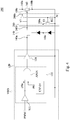
- Fig. 1 is a diagram illustrating a conversion circuit 100 according to some embodiments of the present disclosure. As shown in Fig. 1 , the conversion circuit 100 includes a voltage control circuit 140, a main device 160 and a trigger circuit 180.
- the main device 160 includes a first terminal 160a, a second terminal 160b and a control terminal 160c.
- the second terminal 160b is electrically connected to a reference terminal Nr.
- the control terminal 160c is configured to receive a driving signal S1, so that the main device 160 is driven in response to a first voltage level of the driving signal S1.
- the main device 160 operates in a first state (e.g., a normal working state) and is configured to perform power switching.
- the main device 160 may be the power switching element applied in various switching power supply devices, such as a buck converter, a boost converter, a buck-boost converter or any other devices having power switches.
- the main device 160 may include a Gallium Nitride (GaN) switching device, a MOSFET switching device, an Insulated Gate Bipolar Transistor (IGBT) switching device, a bipolar junction transistor (BJT) switching device, a Silicon Carbide (SiC) switching device, a relay switching device, or any combination thereof.
- GaN Gallium Nitride
- MOSFET MOSFET
- IGBT Insulated Gate Bipolar Transistor
- BJT bipolar junction transistor
- SiC Silicon Carbide
- the voltage control circuit 140 is electrically connected to the main device 160 so as to provide the driving signal S1 to the main device 160.
- the voltage control circuit 140 includes an input terminal 140a, an output terminal 140b and a control terminal 140c.
- the output terminal 140b is electrically connected to the control terminal 160c of the main device160.
- the voltage control circuit 140 is configured to receive an original signal, and output a driving signal S1 to the main device 160 according to the original signal S0.
- the conversion circuit 100 further includes a driving signal generator 120 to generate the original signal S0.
- the driving signal generator 120 is electrically connected to the input terminal 140a of the voltage control circuit 140.
- the driving signal generator 120 includes a logic circuit 122 and a driver buffer 124, and is configured to receive an input voltage VDD from a voltage source and generate the original signal S0. Details will be explained in the following paragraphs.
- the trigger circuit 180 is configured to modify the voltage level at the control terminal 140c, so that the voltage level of the driving signal S1 (i.e., the voltage level of the control terminal 160c) is changed accordingly. For example, the voltage level of the driving signal S1 is temporarily decreased from the first voltage level to the second voltage level.
- the trigger circuit 180 is electrically connected between the control terminal 160c and the control terminal140c.
- the trigger circuit 180 includes an output terminal 180a and a sense terminal 180b.
- the output terminal 180a of the trigger circuit 180 is electrically connected to the control terminal 140c of the voltage control circuit 140, and the sense terminal 180b of the trigger circuit 180 is electrically connected to the control terminal 160c of the main device 160.
- the trigger circuit 180 when the main device 160 is configured to perform power switching according to the driving signal S1 is having the first voltage level, the trigger circuit 180 is configured to turn on in response to a voltage level of the control terminal 160c, to modify a voltage level at the control terminal 140c, so that the voltage control circuit 140 is configured to output the driving signal S1 having a second voltage level.
- the second voltage level is less than the first voltage level.
- the trigger circuit 180 may turn on in response to the voltage level of the control terminal 160c so as to pull low the voltage level at the control terminal 140c.
- the voltage control circuit 140 may decrease the voltage level of the driving signal S1 (e.g., from first voltage level to the second voltage level). Therefore, the main device 160 may perform power switching in a second state, and be protected from damage due to abnormal states (e.g., the abnormal large voltage or the large current).
- the trigger circuit 180 causes the voltage level of the driving signal S1 to have a "two-stage" change.
- the main device 160 is prevented from being damaged by abnormal states such as gate voltage spike without affecting the driving speed of the main device160.
- the trigger circuit 180 includes a first capacitance C1, a first switching unit T1 and a first resistance R1.
- the first capacitance C1 is electrically connected to the control terminal 160c of the main device 160.
- the first switching unit T1 is electrically between the control terminal 140c of the voltage control circuit 140 and a reference terminal Nr (e.g. ground), and a control terminal of the first switching unit T1 is electrically connected to the first capacitance C1.
- Fig. 2 is a waveform diagram of the voltage level change at the control terminal 160c.
- the horizontal axis represents the voltage value between the first resistor R1 and the first capacitor, and the vertical axis represents the voltage value of control terminal 160c.
- the capacitor C1 After a second charging period P2, the capacitor C1 is fully charged, the first switching unit T1 is turned off. At this time, the control terminal 140c returns to a predetermined level, and the voltage level of the driving signal S1 outputted by the voltage control circuit 140 may be controlled into the first voltage level V1.
- the problem that the main device 160 is damaged due to the voltage spike of the driving signal S1 can be avoided when the voltage control circuit 140 is beginning to output the signal S1 having the first voltage level V1.
- the length of time of the first charging period P1 and the second charging period P2 depends on the first capacitance R1 and the first resistance C1.
- the driving signal S1 is generated by the voltage control circuit 140 in response to the voltage level at the control terminal 140c of the voltage control circuit 140.
- the voltage control circuit 140 can use a variety of circuit structures.
- the voltage control circuit 140 includes a voltage control switch 141.
- the a voltage control switch 141 includes a drain terminal, a source terminal and a gate terminal.
- the drain terminal is coupled to the input terminal 140a of the voltage control circuit 140.
- the source terminal is coupled to the output terminal 140b of the voltage control circuit 140.
- the gate terminal is coupled to the control terminal 140c of the voltage control circuit 140.
- the voltage control circuit 140 is normally-on in response to a zero gate-source voltage at the control terminal 140c.
- the voltage control switch 141 may include a depletion type metal-oxide-semiconductor field-effect transistor (MOSFET) switching device to achieve the normally-on operation in response to the zero gate-source voltage at the reference terminal, but the present disclosure is not limited thereto.
- the voltage control switch 141 may include other suitable semiconductor devices having similar channel current to gate voltage characteristics to achieve the voltage control switch 141.
- the voltage control switch 141 may include a depletion type MOSFET switching device, an enhancement type MOSFET switching device, or any combination thereof.
- the voltage control circuit 140 further includes a clamping circuit 142.
- a first terminal 142a of the clamping circuit 142 is electrically connected to the gate terminal of the voltage control switch 140.
- a second terminal 142c of the clamping circuit 142 is electrically connected to a reference terminal Nr.
- a voltage across the first terminal 142a and the second terminal 142b of the clamping circuit 142 is clamped to a predetermined level.
- the clamping circuit 142 comprises at least two Zener diodes Da, Db connected in series.
- the control terminal 140c is between two Zener diodes Da, Db.
- the threshold voltage of the voltage control circuit 140 is negative, and the voltage control circuit 140 is configured to be off on the condition that the gate-source voltage is smaller than the negative threshold voltage Vth.
- the threshold voltage is the threshold voltage of the MOSFET switching device.
- the threshold voltage of the normally-on device is between -0,1 volts and -20 volts.
- the voltage level of the driving signal S1 will be clamped by the voltage control circuit 140 in response to the threshold voltage of the voltage control circuit 140 on the condition that the voltage level of the original signal S0 is higher than a specific value.
- the voltage level of the original signal S0 is higher than the voltage level of the driving signal S1 since the voltage level of the driving signal S1 is clamped by the voltage control circuit 140.
- Fig. 3A and Fig. 3B are diagrams illustrating the voltage control circuit according to some other embodiments of the present disclosure.
- like elements in Fig. 1 are designated with the same reference numbers for ease of understanding.
- the specific operations of similar elements, which are already discussed in detail in the above paragraphs, are omitted herein for the sake of brevity, unless there is a need to introduce the co-operation relationship with the elements shown in Fig. 3A and Fig. 3B .
- the voltage control circuit 240 includes a clamping circuit.
- the clamping circuit includes multiple clamping unit D1, D2 connected in series, and the trigger circuit 180 is electrically connected to the control terminal 240c (i.e., a node between two of the clamping unit D1, D2).
- the clamping unit D1, D2 can be implemented by diodes or Zener diodes.
- the clamping circuit may be realized by multiple MOSFETs electrically coupled to each other. The gate terminal of one of the MOSFETs is electrically coupled to the source terminal or the drain terminal of another one of the MOSFETs.
- the number of the diode units or the MOSFETs may be adjusted according to actual needs and thus the present disclosure is not limited to examples shown in Fig. 3A .
- the original signal S0 is clamped by the clamping circuit of the voltage control circuit 240, and forms the driving signal S1.
- the trigger circuit 180 When the trigger circuit 180 is turned on, the control terminal 160c conducts to the reference terminal Nr, so the voltage level of the driving signal S1 will change accordingly.
- the voltage control circuit 340 includes a buffer 341 and a regulator circuit 342.
- the buffer 341 is electrically connected to the control terminal 160c.
- the regulator circuit 342 is electrically connected to the buffer 341.
- a control terminal of the regulator circuit 342 as the control terminal 340c of the voltage control circuit 340, and is electrically connected to the trigger circuit 180.
- the regulator circuit 342 is output a control voltage Sc to a positive control terminal of the buffer 341 to control the voltage level of the driving signal S1 outputted by the buffer 341.
- the trigger circuit 180 is turned on, the control terminal of the regulator circuit 342 conducts to the reference Nr, so the voltage level of the control terminal of the regulator circuit 342 is decreased.
- the voltage level of the control voltage Sc is modified in response to a voltage level of the control terminal of the regulator circuit 342. Since the person in the art can understand the operation of the regulator circuit 342, it is not explained here.
- the driving signal generator 120 includes a logic circuit 122 and a driver buffer 124, and is configured to receive an input voltage VDD from a voltage source and generate an original signal S0. Specifically, the input voltage VDD is provided to the logic circuit 122 and the driver buffer 124 to supply the required power. In some embodiments, the logic circuit 122 is configured to generate the original signal S0 according to a pulse-width modulation (PWM) signal PWM.
- PWM pulse-width modulation
- the logic circuit 122 may include a Schmitt trigger ST1, an Under-Voltage Lockout (UVLO) circuit UVLO1, and an AND gate AND1.
- the Schmitt trigger is ST1 configured to receive the pulse-width modulation (PWM) signal PWM, and output a signal DSx, in which the value of the signal DSx retains the value until the pulse-width modulation signal PWM at the input terminal changes sufficiently to trigger a change.
- PWM pulse-width modulation
- the Under-Voltage Lockout (UVLO) circuit UVLO1 is configured to monitor the input voltage VDD and provide a protection signal PS1 on the condition that under voltage occurs.
- the AND gate AND1 is coupled to the Schmitt trigger ST1, and the Under-Voltage Lockout (UVLO) circuit UVLO1 at the input side, and perform an AND operation correspondingly to output the original signal S0 in response to the received signals.
- the original signal S0 is transmitted to the driver buffer 124 coupled to the logic circuit 122, and the driver buffer 124 is configured to output the original signal S0 via an output terminal.
- the structure of the driving signal generator 120 is not limited to this.
- Fig. 4 is a diagram illustrating a conversion circuit 100 according to some embodiments of the present disclosure. With respect to the embodiments of Fig. 4 , like elements in Fig. 1 are designated with the same reference numbers for ease of understanding. The specific operations of similar elements, which are already discussed in detail in above paragraphs, are omitted herein for the sake of brevity, unless there is a need to introduce the co-operation relationship with the elements shown in Fig. 4 .
- the conversion circuit 100 includes the driving signal generator 120, the main device 160, the voltage control circuit 140 and a trigger circuit 280.
- the trigger circuit 280 is electrically connected between the first terminal 160a of the main device 160 and the control terminal 140c of the voltage control circuit 140.
- the trigger circuit 280 includes an output terminal 280a and a sense terminal 280b.
- the output terminal 280a of the trigger circuit 280 is electrically connected to the control terminal 140c of the voltage control circuit 140
- the sense terminal 280b of the trigger circuit 180 is electrically connected to the first terminal 160a of the main device 160.
- the voltage control circuit 140 is configured to output the driving signal S1 having a first voltage level to the main device160.
- the main device is configured to perform power switching according to the first voltage level of the driving signal S1.
- the trigger circuit 280 is configured to turn on in response to the operation voltage level of the first terminal 160a, to modify a voltage level at the control terminal 140c so that the voltage control circuit 140 is configured to output the driving signal S1 having a second voltage level, the second voltage level is less than the first voltage level.
- the trigger circuit 280 may turn on in response to the voltage level of the first terminal 160a so as to pull low the voltage level at the control terminal 140c.
- the voltage control circuit 140 may decrease the voltage level of the driving signal S1 (e.g., from first voltage level to the second voltage level). Therefore, the main device 160 may perform power switching in a second state, and be protected from damage due to the gate voltage spike or the abnormal large current.
- the trigger circuit 280 causes the voltage level of the driving signal S1 to have a "two-stage" change. That is, the voltage level of the driving signal S1 maintains to the second voltage level until the first terminal 160a return to the predetermined voltage level and the trigger circuit 280 is turned off accordingly.
- the trigger circuit 280 includes a second switching unit T2, a third switching unit T3, and a second resistance R2.
- the second switching unit T2 is electrically connected between the first terminal 160a and the reference terminal Nr.
- a control terminal of the second switching unit T2 is electrically connected to the output terminal 140b.
- the third switching unit T3 is electrically connected between the control terminal of the voltage control circuit 140c and the reference terminal Nr.
- a control terminal of the third switching unit T3 is electrically connected to the second switching unit T2.
- the second switching unit T2 is further electrically connected to the reference terminal Nr through the second resistance R2.
- the control terminal of the third switching unit T3 is further electrically connected to the reference terminal Nr through the second resistance R2.
- the main device 160 and the second switching unit T2 may turn on and turn off synchronously.
- the third switching unit T3 may turn on to decrease the voltage level of the control terminal 140c of the voltage control circuit 140. Then, the voltage level of the driving signal S1 may be modified to the second voltage level, and the main device 160 is protected from damage due to the large current.
- the trigger circuit 380 includes an output terminal 380a and a sense terminal 380b.
- the output terminal 380a of the trigger circuit 380 is electrically connected to the control terminal 240c of the voltage control circuit 240, and the sense terminal 380b of the trigger circuit 380 is electrically connected to the first terminal 160a of the main device 160.
- the trigger circuit 380 includes a rectifier T4.
- the rectifier T4 is electrically connected between the first terminal 160a of the main device 160 and the control terminal 240c of the voltage control circuit 240.
- the rectifier T4 is configured to turn on.
- the rectifier T4 may turn on to modify (e.g., decrease) the voltage level of the control terminal 240c.
- the rectifier T4 may be a diode, a rectifying element or a single throw switch, but not limited to this.
- the trigger circuit 380 can be applied to the mentioned voltage control circuit 340.
- the trigger circuit 280, 380 can be applied to the voltage control circuit 140, the voltage control circuit 240 or the voltage control circuit 340.
- the voltage control circuit 140 shown in Fig. 4 (or the voltage control circuit 240, 340 as shown in Fig. 5A - B ) is merely one example of various embodiments of the present disclosure and not meant to limit the circuit structure of the voltage control circuit.
- the voltage control circuit in the conversion circuit can be implemented by the other circuit structure, such as the voltage control circuit 140, 240, 340 shown in Fig. 4 - Fig. 5B .
- Fig. 6A-Fig. 6B are diagrams illustrating integration of the voltage control circuit 140, the main device 160 and the trigger circuit 180 according to some embodiments of the present disclosure.
- the normally-on voltage control switch 141, the main device 160 and the trigger circuit 180 are integrated or packaged together with System on Chip (SoC) on a substrate 610a to form a chip 600a.
- SoC System on Chip
- the normally-on voltage control switch 141, the main device 160 and the trigger circuit 180 are integrated or packaged together with System in Package (SiP) on a substrate 610b to form a package 600b.
- SiP dies may be stacked vertically or tiled horizontally and internally connected by wires that are bonded to the package.
- the voltage control circuit 140, the main device 160 and the trigger circuit 180 may be integrated or packaged together with System in Package, System on Chip, three-dimensional integrated circuit (3D IC), etc.
- Fig. 7A and Fig. 7B are diagrams illustrating integration of the driving signal generator 120 and the voltage control circuit 140 according to some embodiments of the present disclosure.
- the logic circuit 122, the driver buffer 124, and the voltage control circuit 140 are integrated or packaged together with System on Chip (SoC) on a substrate 710a to form a chip 700a.
- SoC System on Chip
- the logic circuit 122, the driver buffer 124, and the voltage control circuit 140 are integrated or packaged together with System in Package (SiP) on a substrate 710b to form a package 700b.
- SiP System in Package
- the driving signal generator 120 and the voltage control circuit 140 may be integrated or packaged together with System in Package, System on Chip, 3D IC, etc.
- the driving signal generator 120, the voltage control circuit 140, the main device 160 and the trigger circuit 180 may also be integrated or packaged together with System in Package, System on Chip, 3D IC, etc, and further explanation is omitted herein for the sake of brevity.
- the elements in the above embodiments may be implemented by various digital or analog circuits, and may also be implemented by different integrated circuit chips. Each element may also be integrated in a single chip.
- the circuits may be realized by a microcontroller unit (MCU), or by be realized in various ways such as by a digital signal processor (DSP), a field-programmable gate array (FPGA), etc.
- the switches and transistors may be realized by proper devices.
- the switches may be implemented by power semiconductor devices including but not limited to Insulated Gate Bipolar Transistors (IGBTs), bipolar junction transistors (BJTs), SiC metal-oxide-semiconductor field-effect transistors (MOSFET), or mechanical switches, such as various types of relays.
- IGBTs Insulated Gate Bipolar Transistors
- BJTs bipolar junction transistors
- MOSFET SiC metal-oxide-semiconductor field-effect transistors
- mechanical switches such as various types of relays.
- the normally-on switching devices may be GaN transistors or semiconductors devices with similar I-V characteristics.
- Transformer, diodes, resistors, capacitor units and/or inductors units may be realized by suitable electronic elements. The above list is merely exemplary and is not meant to be limitations of the present disclosure.
Landscapes
- Engineering & Computer Science (AREA)
- Power Engineering (AREA)
- Power Conversion In General (AREA)
Abstract
Description
- The present disclosure relates to a power supply device, and in particular, to a conversion circuit in the power supply device.
- For existing conversion circuit for the power converters, the supplying voltage is designed in response to the rated voltage of the semiconductor device to be driven. Therefore, one or more additional voltage regulators are required to regulate the system supplying power to meet the voltage requirement of the conversion circuit and the semiconductor device.
- One aspect of the present disclosure is a conversion circuit. The conversion circuit includes a main device, a voltage control circuit and a trigger circuit. The main device includes a control terminal. The voltage control circuit includes an output terminal and a control terminal. The output terminal of the voltage control circuit is electrically connected to the control terminal of the main device. The voltage control circuit is configured to output a driving signal having a first voltage level to the main device. The trigger circuit comprises an output terminal and a sense terminal. The output terminal of the trigger circuit is electrically connected to the control terminal of the voltage control circuit. The sense terminal of the trigger circuit is electrically connected to the control terminal of the main device. It is to be understood that both the foregoing general description and the following detailed description are by examples, and are intended to provide further explanation of the disclosure as claimed.
- The present disclosure can be more fully understood by reading the following detailed description of the embodiment, with reference made to the accompanying drawings as follows:
-
Fig. 1 is a schematic diagram of a conversion circuit in some embodiments of the present disclosure. -
Fig 2 is a voltage waveform diagram of the control terminal of main device in some embodiments of the present disclosure. -
Fig. 3A is a schematic diagram of a conversion circuit in some embodiments of the present disclosure. -
Fig. 3B is a schematic diagram of a conversion circuit in some embodiments of the present disclosure. -
Fig. 4 is a schematic diagram of a conversion circuit in some embodiments of the present disclosure. -
Fig. 5A is a schematic diagram of a conversion circuit in some embodiments of the present disclosure. -
Fig. 5B is a schematic diagram of a conversion circuit in some embodiments of the present disclosure. -
Fig. 6A - Fig. 6B are diagrams illustrating integration of the voltage control circuit, the main device and a trigger circuit according to some embodiments of the present disclosure. -
Fig. 7A and Fig. 7B are diagrams illustrating integration of the driving signal generator and the voltage control circuit according to some embodiments of the present disclosure. - For the embodiment below is described in detail with the accompanying drawings, embodiments are not provided to limit the scope of the present disclosure. Moreover, the operation of the described structure is not for limiting the order of implementation. Any device with equivalent functions that is produced from a structure formed by a recombination of elements is all covered by the scope of the present disclosure. Drawings are for the purpose of illustration only, and not plotted in accordance with the original size.
- It will be understood that when an element is referred to as being "connected to" or "coupled to", it can be directly connected or coupled to the other element or intervening elements may be present. In contrast, when an element to another element is referred to as being "directly connected" or "directly coupled," there are no intervening elements present. As used herein, the term "and/or" includes an associated listed items or any and all combinations of more.
- Reference is made to
Fig. 1. Fig. 1 is a diagram illustrating aconversion circuit 100 according to some embodiments of the present disclosure. As shown inFig. 1 , theconversion circuit 100 includes avoltage control circuit 140, amain device 160 and atrigger circuit 180. - In structural, the
main device 160 includes afirst terminal 160a, asecond terminal 160b and acontrol terminal 160c. Thesecond terminal 160b is electrically connected to a reference terminal Nr. Thecontrol terminal 160c is configured to receive a driving signal S1, so that themain device 160 is driven in response to a first voltage level of the driving signal S1. Themain device 160 operates in a first state (e.g., a normal working state) and is configured to perform power switching. In various embodiments of the present disclosure, themain device 160 may be the power switching element applied in various switching power supply devices, such as a buck converter, a boost converter, a buck-boost converter or any other devices having power switches. For example, themain device 160 may include a Gallium Nitride (GaN) switching device, a MOSFET switching device, an Insulated Gate Bipolar Transistor (IGBT) switching device, a bipolar junction transistor (BJT) switching device, a Silicon Carbide (SiC) switching device, a relay switching device, or any combination thereof. - The
voltage control circuit 140 is electrically connected to themain device 160 so as to provide the driving signal S1 to themain device 160. In some embodiments, thevoltage control circuit 140 includes aninput terminal 140a, anoutput terminal 140b and acontrol terminal 140c. Theoutput terminal 140b is electrically connected to thecontrol terminal 160c of the main device160. Thevoltage control circuit 140 is configured to receive an original signal, and output a driving signal S1 to themain device 160 according to the original signal S0. - In some embodiments, the
conversion circuit 100 further includes adriving signal generator 120 to generate the original signal S0. Thedriving signal generator 120 is electrically connected to theinput terminal 140a of thevoltage control circuit 140. Thedriving signal generator 120 includes alogic circuit 122 and adriver buffer 124, and is configured to receive an input voltage VDD from a voltage source and generate the original signal S0. Details will be explained in the following paragraphs. - The
trigger circuit 180 is configured to modify the voltage level at thecontrol terminal 140c, so that the voltage level of the driving signal S1 (i.e., the voltage level of thecontrol terminal 160c) is changed accordingly. For example, the voltage level of the driving signal S1 is temporarily decreased from the first voltage level to the second voltage level. - In some embodiments, the
trigger circuit 180 is electrically connected between thecontrol terminal 160c and the control terminal140c. Thetrigger circuit 180 includes anoutput terminal 180a and asense terminal 180b. Theoutput terminal 180a of thetrigger circuit 180 is electrically connected to thecontrol terminal 140c of thevoltage control circuit 140, and thesense terminal 180b of thetrigger circuit 180 is electrically connected to thecontrol terminal 160c of themain device 160. - In some embodiments, when the
main device 160 is configured to perform power switching according to the driving signal S1 is having the first voltage level, thetrigger circuit 180 is configured to turn on in response to a voltage level of thecontrol terminal 160c, to modify a voltage level at thecontrol terminal 140c, so that thevoltage control circuit 140 is configured to output the driving signal S1 having a second voltage level. The second voltage level is less than the first voltage level. - Accordingly, at the moment when the
main device 160 is turned on in response to the driving signal S1, thetrigger circuit 180 may turn on in response to the voltage level of thecontrol terminal 160c so as to pull low the voltage level at thecontrol terminal 140c. At this time, thevoltage control circuit 140 may decrease the voltage level of the driving signal S1 (e.g., from first voltage level to the second voltage level). Therefore, themain device 160 may perform power switching in a second state, and be protected from damage due to abnormal states (e.g., the abnormal large voltage or the large current). In summary, thetrigger circuit 180 causes the voltage level of the driving signal S1 to have a "two-stage" change. Thus, in the present disclosure, themain device 160 is prevented from being damaged by abnormal states such as gate voltage spike without affecting the driving speed of the main device160. - In some embodiments, the
trigger circuit 180 includes a first capacitance C1, a first switching unit T1 and a first resistance R1. The first capacitance C1 is electrically connected to thecontrol terminal 160c of themain device 160. The first switching unit T1 is electrically between thecontrol terminal 140c of thevoltage control circuit 140 and a reference terminal Nr (e.g. ground), and a control terminal of the first switching unit T1 is electrically connected to the first capacitance C1. - Referring to the
Fig. 2, Fig. 2 is a waveform diagram of the voltage level change at thecontrol terminal 160c. The horizontal axis represents the voltage value between the first resistor R1 and the first capacitor, and the vertical axis represents the voltage value ofcontrol terminal 160c. When themain device 160 is turned on in response to the first voltage level of the driving signal S1, the first capacitor begins to be charged, and the control terminal of the first switching unit T1 conducts to thecontrol terminal 160c. In a first charging period P1, when the voltage level between the first resistor R1 and the first capacitance C1 reaches to the threshold voltage of the first switching unit T1, the first switching unit T1 will be turned on according to the voltage level of thecontrol terminal 160c. At this time, since thecontrol terminal 140c is pulled low to the reference terminal Nr, the voltage level of the driving signal S1 outputted by thevoltage control circuit 140 may be controlled into the second voltage level V2. - After a second charging period P2, the capacitor C1 is fully charged, the first switching unit T1 is turned off. At this time, the
control terminal 140c returns to a predetermined level, and the voltage level of the driving signal S1 outputted by thevoltage control circuit 140 may be controlled into the first voltage level V1. Through the foregoing features, the problem that themain device 160 is damaged due to the voltage spike of the driving signal S1 can be avoided when thevoltage control circuit 140 is beginning to output the signal S1 having the first voltage level V1. The length of time of the first charging period P1 and the second charging period P2 depends on the first capacitance R1 and the first resistance C1. - The driving signal S1 is generated by the
voltage control circuit 140 in response to the voltage level at thecontrol terminal 140c of thevoltage control circuit 140. Thevoltage control circuit 140 can use a variety of circuit structures. In some embodiments, thevoltage control circuit 140 includes avoltage control switch 141. The avoltage control switch 141 includes a drain terminal, a source terminal and a gate terminal. The drain terminal is coupled to theinput terminal 140a of thevoltage control circuit 140. The source terminal is coupled to theoutput terminal 140b of thevoltage control circuit 140. The gate terminal is coupled to thecontrol terminal 140c of thevoltage control circuit 140. - The
voltage control circuit 140 is normally-on in response to a zero gate-source voltage at thecontrol terminal 140c. Thevoltage control switch 141 may include a depletion type metal-oxide-semiconductor field-effect transistor (MOSFET) switching device to achieve the normally-on operation in response to the zero gate-source voltage at the reference terminal, but the present disclosure is not limited thereto. In some other embodiments, thevoltage control switch 141 may include other suitable semiconductor devices having similar channel current to gate voltage characteristics to achieve thevoltage control switch 141. Alternatively stated, thevoltage control switch 141 may include a depletion type MOSFET switching device, an enhancement type MOSFET switching device, or any combination thereof. - In some embodiments, the
voltage control circuit 140 further includes aclamping circuit 142. A first terminal 142a of theclamping circuit 142 is electrically connected to the gate terminal of thevoltage control switch 140. A second terminal 142c of theclamping circuit 142 is electrically connected to a reference terminal Nr. A voltage across thefirst terminal 142a and the second terminal 142b of theclamping circuit 142 is clamped to a predetermined level. In some embodiments, theclamping circuit 142 comprises at least two Zener diodes Da, Db connected in series. Thecontrol terminal 140c is between two Zener diodes Da, Db. The threshold voltage of thevoltage control circuit 140 is negative, and thevoltage control circuit 140 is configured to be off on the condition that the gate-source voltage is smaller than the negative threshold voltage Vth. In some embodiments, the threshold voltage is the threshold voltage of the MOSFET switching device. For example, in some embodiments, the threshold voltage of the normally-on device is between -0,1 volts and -20 volts. - Accordingly, the voltage level of the driving signal S1 will be clamped by the
voltage control circuit 140 in response to the threshold voltage of thevoltage control circuit 140 on the condition that the voltage level of the original signal S0 is higher than a specific value. Alternatively stated, the voltage level of the original signal S0 is higher than the voltage level of the driving signal S1 since the voltage level of the driving signal S1 is clamped by thevoltage control circuit 140. - Reference is made to
Fig. 3A and Fig. 3B. Fig. 3A and Fig. 3B are diagrams illustrating the voltage control circuit according to some other embodiments of the present disclosure. With respect to the embodiments ofFig. 3A and Fig. 3B , like elements inFig. 1 are designated with the same reference numbers for ease of understanding. The specific operations of similar elements, which are already discussed in detail in the above paragraphs, are omitted herein for the sake of brevity, unless there is a need to introduce the co-operation relationship with the elements shown inFig. 3A and Fig. 3B . - In some other embodiments, referring the
Fig. 3A , thevoltage control circuit 240 includes a clamping circuit. The clamping circuit includes multiple clamping unit D1, D2 connected in series, and thetrigger circuit 180 is electrically connected to thecontrol terminal 240c (i.e., a node between two of the clamping unit D1, D2). In some alternative embodiments, the clamping unit D1, D2 can be implemented by diodes or Zener diodes. In some other embodiments, the clamping circuit may be realized by multiple MOSFETs electrically coupled to each other. The gate terminal of one of the MOSFETs is electrically coupled to the source terminal or the drain terminal of another one of the MOSFETs. The number of the diode units or the MOSFETs may be adjusted according to actual needs and thus the present disclosure is not limited to examples shown inFig. 3A . The original signal S0 is clamped by the clamping circuit of thevoltage control circuit 240, and forms the driving signal S1. When thetrigger circuit 180 is turned on, thecontrol terminal 160c conducts to the reference terminal Nr, so the voltage level of the driving signal S1 will change accordingly. - In some other embodiments, referring the
Fig. 3B , thevoltage control circuit 340 includes abuffer 341 and aregulator circuit 342. Thebuffer 341 is electrically connected to thecontrol terminal 160c. Theregulator circuit 342 is electrically connected to thebuffer 341. A control terminal of theregulator circuit 342 as thecontrol terminal 340c of thevoltage control circuit 340, and is electrically connected to thetrigger circuit 180. Theregulator circuit 342 is output a control voltage Sc to a positive control terminal of thebuffer 341 to control the voltage level of the driving signal S1 outputted by thebuffer 341. When thetrigger circuit 180 is turned on, the control terminal of theregulator circuit 342 conducts to the reference Nr, so the voltage level of the control terminal of theregulator circuit 342 is decreased. At this time, the voltage level of the control voltage Sc is modified in response to a voltage level of the control terminal of theregulator circuit 342. Since the person in the art can understand the operation of theregulator circuit 342, it is not explained here. - In addition, referring to
Fig. 1 , in some embodiments, the drivingsignal generator 120 includes alogic circuit 122 and adriver buffer 124, and is configured to receive an input voltage VDD from a voltage source and generate an original signal S0. Specifically, the input voltage VDD is provided to thelogic circuit 122 and thedriver buffer 124 to supply the required power. In some embodiments, thelogic circuit 122 is configured to generate the original signal S0 according to a pulse-width modulation (PWM) signal PWM. - For example, as shown in
Fig. 1 , thelogic circuit 122 may include a Schmitt trigger ST1, an Under-Voltage Lockout (UVLO) circuit UVLO1, and an AND gate AND1. The Schmitt trigger is ST1 configured to receive the pulse-width modulation (PWM) signal PWM, and output a signal DSx, in which the value of the signal DSx retains the value until the pulse-width modulation signal PWM at the input terminal changes sufficiently to trigger a change. - The Under-Voltage Lockout (UVLO) circuit UVLO1 is configured to monitor the input voltage VDD and provide a protection signal PS1 on the condition that under voltage occurs. The AND gate AND1 is coupled to the Schmitt trigger ST1, and the Under-Voltage Lockout (UVLO) circuit UVLO1 at the input side, and perform an AND operation correspondingly to output the original signal S0 in response to the received signals. The original signal S0 is transmitted to the
driver buffer 124 coupled to thelogic circuit 122, and thedriver buffer 124 is configured to output the original signal S0 via an output terminal. However, the structure of the drivingsignal generator 120 is not limited to this. - In the foregoing embodiment, the
trigger circuit 180 is turned on in response to a voltage level of thecontrol terminal 160c. However, in some other embodiments, thetrigger circuit 180 may turn on in response to a voltage level of other terminals of themain device 160. Reference is made toFig. 4. Fig. 4 is a diagram illustrating aconversion circuit 100 according to some embodiments of the present disclosure. With respect to the embodiments ofFig. 4 , like elements inFig. 1 are designated with the same reference numbers for ease of understanding. The specific operations of similar elements, which are already discussed in detail in above paragraphs, are omitted herein for the sake of brevity, unless there is a need to introduce the co-operation relationship with the elements shown inFig. 4 . - As shown in
Fig. 4 , in structural, theconversion circuit 100 includes the drivingsignal generator 120, themain device 160, thevoltage control circuit 140 and atrigger circuit 280. Thetrigger circuit 280 is electrically connected between the first terminal 160a of themain device 160 and thecontrol terminal 140c of thevoltage control circuit 140. In some other embodiments, thetrigger circuit 280 includes anoutput terminal 280a and asense terminal 280b. Theoutput terminal 280a of thetrigger circuit 280 is electrically connected to thecontrol terminal 140c of thevoltage control circuit 140, and thesense terminal 280b of thetrigger circuit 180 is electrically connected to the first terminal 160a of themain device 160. - When the
main device 160 operates in the first state, and thefirst terminal 160a has a predetermined voltage level, thevoltage control circuit 140 is configured to output the driving signal S1 having a first voltage level to the main device160. The main device is configured to perform power switching according to the first voltage level of the driving signal S1. On the other hand, when the first terminal 160a of themain device 160 has an operation voltage level different from the predetermined voltage level, for example, the operation voltage level is much larger than the predetermined voltage level, or a large current through themain device 160, at this time, thetrigger circuit 280 is configured to turn on in response to the operation voltage level of thefirst terminal 160a, to modify a voltage level at thecontrol terminal 140c so that thevoltage control circuit 140 is configured to output the driving signal S1 having a second voltage level, the second voltage level is less than the first voltage level. - Accordingly, in the situation that the
main device 160 operates in the first state and performs power switching, if there is a large current, which exceeding a preset range, through themain device 160, thetrigger circuit 280 may turn on in response to the voltage level of thefirst terminal 160a so as to pull low the voltage level at thecontrol terminal 140c. At this time, thevoltage control circuit 140 may decrease the voltage level of the driving signal S1 (e.g., from first voltage level to the second voltage level). Therefore, themain device 160 may perform power switching in a second state, and be protected from damage due to the gate voltage spike or the abnormal large current. Same as the previous embodiment, thetrigger circuit 280 causes the voltage level of the driving signal S1 to have a "two-stage" change. That is, the voltage level of the driving signal S1 maintains to the second voltage level until thefirst terminal 160a return to the predetermined voltage level and thetrigger circuit 280 is turned off accordingly. - Referring to the
Fig. 4 , in some embodiments, thetrigger circuit 280 includes a second switching unit T2, a third switching unit T3, and a second resistance R2. The second switching unit T2 is electrically connected between thefirst terminal 160a and the reference terminal Nr. A control terminal of the second switching unit T2 is electrically connected to theoutput terminal 140b. The third switching unit T3 is electrically connected between the control terminal of thevoltage control circuit 140c and the reference terminal Nr. A control terminal of the third switching unit T3 is electrically connected to the second switching unit T2. In some embodiments, the second switching unit T2 is further electrically connected to the reference terminal Nr through the second resistance R2. The control terminal of the third switching unit T3 is further electrically connected to the reference terminal Nr through the second resistance R2. - Since the voltage across the second switching unit T2 is same as the
main device 160, themain device 160 and the second switching unit T2 may turn on and turn off synchronously. When thefirst terminal 160a has an operation voltage level different from the predetermined voltage level, the third switching unit T3 may turn on to decrease the voltage level of thecontrol terminal 140c of thevoltage control circuit 140. Then, the voltage level of the driving signal S1 may be modified to the second voltage level, and themain device 160 is protected from damage due to the large current. - With respect to the embodiments of
Fig. 5A-5B , like elements inFig. 1 are designated with the same reference numbers for ease of understanding. The specific operations of similar elements, which are already discussed in detail in above paragraphs, are omitted herein for the sake of brevity, unless there is a need to introduce the co-operation relationship with the elements shown inFig. 5A-5B . Referring toFig. 5A , in other some embodiments, thetrigger circuit 380 includes anoutput terminal 380a and asense terminal 380b. Theoutput terminal 380a of thetrigger circuit 380 is electrically connected to thecontrol terminal 240c of thevoltage control circuit 240, and thesense terminal 380b of thetrigger circuit 380 is electrically connected to the first terminal 160a of themain device 160. - The
trigger circuit 380 includes a rectifier T4. The rectifier T4 is electrically connected between the first terminal 160a of themain device 160 and thecontrol terminal 240c of thevoltage control circuit 240. When a voltage across the rectifier T4 is larger than a forward voltage, the rectifier T4 is configured to turn on. For example, in the situation that themain device 160 is inverse turned on, if the current through themain device 160 become larger so as to thefirst terminal 160a has an operation voltage level different from the predetermined voltage level, the rectifier T4 may turn on to modify (e.g., decrease) the voltage level of thecontrol terminal 240c. The rectifier T4 may be a diode, a rectifying element or a single throw switch, but not limited to this. - Referring to
Fig. 5B , thetrigger circuit 380 can be applied to the mentionedvoltage control circuit 340. Similarly, in the embodiments shown inFigures 4 ,5A, and 5B , thetrigger circuit voltage control circuit 140, thevoltage control circuit 240 or thevoltage control circuit 340. Alternatively stated, thevoltage control circuit 140 shown inFig. 4 (or thevoltage control circuit Fig. 5A - B ) is merely one example of various embodiments of the present disclosure and not meant to limit the circuit structure of the voltage control circuit. The voltage control circuit in the conversion circuit can be implemented by the other circuit structure, such as thevoltage control circuit Fig. 4 - Fig. 5B . - Reference is made to
Fig. 6A-Fig. 6B. Fig. 6A-Fig. 6B are diagrams illustrating integration of thevoltage control circuit 140, themain device 160 and thetrigger circuit 180 according to some embodiments of the present disclosure. - Corresponding to the embodiments shown in
Fig. 1 , as shown inFig. 6A , in some embodiments, the normally-onvoltage control switch 141, themain device 160 and thetrigger circuit 180 are integrated or packaged together with System on Chip (SoC) on asubstrate 610a to form achip 600a. As shown inFig. 6B , in some embodiments, the normally-onvoltage control switch 141, themain device 160 and thetrigger circuit 180 are integrated or packaged together with System in Package (SiP) on asubstrate 610b to form apackage 600b. In various embodiments, SiP dies may be stacked vertically or tiled horizontally and internally connected by wires that are bonded to the package. - In other words, in various embodiments, the
voltage control circuit 140, themain device 160 and thetrigger circuit 180 may be integrated or packaged together with System in Package, System on Chip, three-dimensional integrated circuit (3D IC), etc. - Reference is made to
Fig. 7A and Fig. 7B. Fig. 7A and Fig. 7B are diagrams illustrating integration of the drivingsignal generator 120 and thevoltage control circuit 140 according to some embodiments of the present disclosure. - Corresponding to the embodiments shown in
Fig. 1 , as shown inFig. 7A , in some embodiments, thelogic circuit 122, thedriver buffer 124, and thevoltage control circuit 140 are integrated or packaged together with System on Chip (SoC) on asubstrate 710a to form achip 700a.. As shown inFig. 7B , in some embodiments, thelogic circuit 122, thedriver buffer 124, and thevoltage control circuit 140 are integrated or packaged together with System in Package (SiP) on asubstrate 710b to form apackage 700b. - In other words, in various embodiments, similar to the integration applied to the
voltage control circuit 140 and themain device 160, in some embodiments, the drivingsignal generator 120 and thevoltage control circuit 140 may be integrated or packaged together with System in Package, System on Chip, 3D IC, etc. - In some other embodiments, the driving
signal generator 120, thevoltage control circuit 140, themain device 160 and thetrigger circuit 180 may also be integrated or packaged together with System in Package, System on Chip, 3D IC, etc, and further explanation is omitted herein for the sake of brevity. - In addition, the elements in the above embodiments may be implemented by various digital or analog circuits, and may also be implemented by different integrated circuit chips. Each element may also be integrated in a single chip. It is noted that, in an actual implementation, the circuits may be realized by a microcontroller unit (MCU), or by be realized in various ways such as by a digital signal processor (DSP), a field-programmable gate array (FPGA), etc. The switches and transistors may be realized by proper devices. For example, the switches may be implemented by power semiconductor devices including but not limited to Insulated Gate Bipolar Transistors (IGBTs), bipolar junction transistors (BJTs), SiC metal-oxide-semiconductor field-effect transistors (MOSFET), or mechanical switches, such as various types of relays. The normally-on switching devices may be GaN transistors or semiconductors devices with similar I-V characteristics. Transformer, diodes, resistors, capacitor units and/or inductors units may be realized by suitable electronic elements. The above list is merely exemplary and is not meant to be limitations of the present disclosure.
- The elements, method steps, or technical features in the foregoing embodiments may be combined with each other, and are not limited to the order of the specification description or the order of the drawings in the present disclosure.
Claims (14)
- A conversion circuit, characterized by comprising:a main device (160) comprising a control terminal (160c);characterized in that:a voltage control circuit (140,240,340) comprising an output terminal (140b,240b,340b) and a control terminal (140c,240c,340c), the output terminal of the voltage control circuit (140,240,340) electrically connected to the control terminal of the main device (160), wherein the voltage control circuit (140,240,340) is configured to output a driving signal (S1) having a first voltage level to the main device (160); anda trigger circuit (180,280,380) comprising an output terminal (180a,280a,380a) and a sense terminal (180b,280b,380b), wherein the output terminal (180a,280a,380a) of the trigger circuit (180,280,380) is electrically connected to the control terminal (140c,240c,340c) of the voltage control circuit (140,240,340), the sense terminal (180b,280b,380b) of the trigger circuit (180,280,380) is electrically connected to the main device (160).
- The conversion circuit of claim 1, wherein the sense terminal (180b,280b,380b) of the trigger circuit (180,280,380) is electrically connected to the control terminal of the main device (160), when the main device (160) is configured to perform power switching according to the driving signal, the trigger circuit (180,280,380) is configured to turn on in response to a voltage level of the control terminal (160c) of the main device (160), to modify a voltage level at the control terminal (140c,240c,340c) of the voltage control circuit (140,240,340) so that the voltage control circuit (140,240,340) is configured to output the driving signal having a second voltage level.
- The conversion circuit of any one of claim 1 and 2, wherein the trigger circuit (180,280,380) comprises:a first capacitance (C1) electrically connected to the control terminal (160c) of the main device (160); anda first switching unit (T1) electrically between the control terminal (140c,240c,340c) of the voltage control circuit (140,240,340) and a reference terminal, and a control terminal of the first switching unit (T1) electrically connected to the first capacitance (C1).
- The conversion circuit of any one of claim 1, 2 and 3, wherein the main device (160) further comprises a first terminal (160a) electrically connected to the sense terminal(280b, 380b) of the trigger circuit (280,380), when the first terminal (160a) of the main device (160) has a predetermined voltage level, the voltage control circuit (240,340) is configured to output the driving signal having the first voltage level to the main device (160), and the main device (160) is configured to perform power switching according to the first voltage level of the driving signal;
when the first terminal (160a) of the main device (160) has an operation voltage level different from the predetermined voltage level, the trigger circuit (280,380) is configured to turn on in response to the operation voltage level of the first terminal of the main device (160), to modify a voltage level at the control terminal (240c,340c) of the voltage control circuit (240,340) so that the voltage control circuit (240,340) is configured to output the driving signal having a second voltage level. - The conversion circuit of claim 4, wherein a second terminal (160b) of the main device (160) is electrically connected to a reference terminal, and the trigger circuit (280,380) comprises:a second switching unit (T2) electrically connected between the first terminal (160a) of the main device (160) and the reference terminal, and a control terminal of the second switching unit (T2) is electrically connected to the output terminal (140a) of the voltage control circuit (140); anda third switching unit (T3) electrically connected between the control terminal (140c) of the voltage control circuit (240,340) and the reference terminal, and a control terminal of the third switching unit (T3) is electrically connected to the second switching unit (T2).
- The conversion circuit of claim 4, wherein the trigger circuit (280,380) comprises:
a rectifier (T4) electrically connected between the first terminal (160a) of the main device (160) and the control terminal (240c,340c) of the voltage control switching circuit (240, 340), wherein when a voltage across the rectifier is larger than a forward voltage, the rectifier (T4) is configured to turn on. - The conversion circuit of any one of claim 1, 2, 3, 4, 5 and 6, wherein the driving signal (S1) is generated by the voltage control circuit (140,240,340) in response to the voltage level at the control terminal (140c,240c,340c) of the voltage control circuit (140,240,340).
- The conversion circuit of claim 7, wherein the voltage control circuit (140) comprises:
a voltage control switch comprising:a drain terminal coupled to an input terminal of the voltage control circuit (140);a source terminal coupled to the output terminal of the voltage control circuit (140);a gate terminal coupled to the control terminal (140c) of the voltage control circuit (140); anda clamping circuit (142), comprising:a first terminal (142a) electrically connected to the gate terminal of the voltage control switch (141); anda second terminal (142b) electrically connected to a reference terminal, wherein a voltage across the first terminal (142a) and the second terminal (142b) of the clamping circuit (142) is clamped to a predetermined level. - The conversion circuit of any one of claim 1, 2, 3, 4, 5, 6 and 7, wherein the voltage control circuit (140,240) comprises a clamping circuit.
- The conversion circuit of claim 9, wherein the clamping circuit comprises a plurality of clamping units (D1,D2) connected in series, and the trigger circuit (180, 280) is electrically connected between two of the clamping units (D1,D2).
- The conversion circuit of any one of claim 1, 2, 3, 4, 5, 6 and 7, wherein the voltage control circuit (340) comprises:a buffer (341) electrically connected to the control terminal (160c) of the main device (160); anda regulator circuit (342) electrically connected to the buffer (341), wherein a control terminal of the regulator circuit (342) is electrically connected to the trigger circuit (180).
- The conversion circuit of claim 11, wherein the regulator circuit (342) is configured to output a control voltage to the buffer (341) to control the voltage level of the driving signal, and a voltage level of the control voltage is modified in response to a voltage level of the control terminal of the regulator circuit (342).
- The conversion circuit of any one of claim 1, 2, 3, 4, 5, 6, 7, 8, 9, 10, 11 and 12, wherein the main device (160) comprises a GaN switching device, a MOSFET switching device, an IGBT switching device, a BJT switching device, a SiC switching device, a relay switching device, or any combination thereof.
- The conversion circuit of any one of claim 1, 2, 3, 4, 5, 6, 7, 8, 9, 10, 11, 12 and 13, wherein the voltage control circuit (140,240,340), the main device (160) and the trigger circuit are integrated or packaged together with system in package, system on chip, or 3D IC.
Applications Claiming Priority (1)
| Application Number | Priority Date | Filing Date | Title |
|---|---|---|---|
| US16/547,561 US10784795B1 (en) | 2019-08-21 | 2019-08-21 | Conversion circuit |
Publications (1)
| Publication Number | Publication Date |
|---|---|
| EP3783801A1 true EP3783801A1 (en) | 2021-02-24 |
Family
ID=68944563
Family Applications (1)
| Application Number | Title | Priority Date | Filing Date |
|---|---|---|---|
| EP19217388.8A Withdrawn EP3783801A1 (en) | 2019-08-21 | 2019-12-18 | Conversion circuit |
Country Status (4)
| Country | Link |
|---|---|
| US (1) | US10784795B1 (en) |
| EP (1) | EP3783801A1 (en) |
| CN (1) | CN112421955B (en) |
| TW (1) | TWI727730B (en) |
Families Citing this family (4)
| Publication number | Priority date | Publication date | Assignee | Title |
|---|---|---|---|---|
| CN112532083B (en) * | 2020-12-15 | 2021-11-23 | 南京微盟电子有限公司 | Switching power supply constant current output control system in continuous conduction mode |
| TWI771126B (en) | 2021-04-20 | 2022-07-11 | 立錡科技股份有限公司 | Spike suppression circuit, power converter, and control method thereof |
| US12537438B2 (en) * | 2022-01-21 | 2026-01-27 | Infsitronix Technology Corporation | Switch control module of switch mode power supply |
| US12456860B2 (en) * | 2023-11-30 | 2025-10-28 | Ancora Semiconductors Inc. | Clamp circuit |
Citations (6)
| Publication number | Priority date | Publication date | Assignee | Title |
|---|---|---|---|---|
| EP2009792A2 (en) * | 2007-06-27 | 2008-12-31 | Mitsubishi Electric Corporation | Gate drive apparatus |
| US20130301170A1 (en) * | 2012-05-08 | 2013-11-14 | General Electric Company | Systems, methods, and apparatus for voltage clamp circuits |
| US20130328610A1 (en) * | 2012-05-31 | 2013-12-12 | Renesas Electronics Corporation | Semiconductor device |
| US20140111253A1 (en) * | 2012-10-18 | 2014-04-24 | Denso Corporation | Driver for switching element and control system for machine using the same |
| US20140320198A1 (en) * | 2011-11-07 | 2014-10-30 | Siemens Aktiengesellschaft | Protective device for a voltage-controlled semiconductor switch |
| US20170359055A1 (en) * | 2016-06-09 | 2017-12-14 | Richtek Technology Corporation | Driving stage circuit |
Family Cites Families (9)
| Publication number | Priority date | Publication date | Assignee | Title |
|---|---|---|---|---|
| JP3635466B2 (en) * | 2002-09-30 | 2005-04-06 | 日本テキサス・インスツルメンツ株式会社 | Level shift circuit |
| TWI501692B (en) | 2011-07-05 | 2015-09-21 | Green Solution Tech Co Ltd | Led driving circuit with open-circuit protection |
| CN104782033B (en) * | 2012-11-09 | 2018-08-10 | 株式会社村田制作所 | Soft Start of Resonant Converter |
| JP2018061301A (en) * | 2016-10-03 | 2018-04-12 | 株式会社日立製作所 | Semiconductor drive device and power conversion device using the same |
| TWI627826B (en) | 2017-05-16 | 2018-06-21 | 力林科技股份有限公司 | Power conversion apparatus and synchronous rectification controller thereof |
| JP2019047621A (en) * | 2017-09-01 | 2019-03-22 | ミツミ電機株式会社 | Semiconductor device for power supply control, power supply device, and discharge method of x capacitor |
| US10734882B2 (en) * | 2018-02-09 | 2020-08-04 | Delta Electronics, Inc. | Conversion circuit |
| CN109067159B (en) * | 2018-09-14 | 2019-11-12 | 上海南芯半导体科技有限公司 | A kind of soft start controller and load switching device of load switching device |
| CN110011523B (en) * | 2019-04-28 | 2023-12-29 | 苏州蓝博控制技术有限公司 | Power driving phase inverter and low-end driving to high-end driving circuit |
-
2019
- 2019-08-21 US US16/547,561 patent/US10784795B1/en active Active
- 2019-12-18 EP EP19217388.8A patent/EP3783801A1/en not_active Withdrawn
-
2020
- 2020-04-01 CN CN202010248738.5A patent/CN112421955B/en active Active
- 2020-04-01 TW TW109111109A patent/TWI727730B/en active
Patent Citations (6)
| Publication number | Priority date | Publication date | Assignee | Title |
|---|---|---|---|---|
| EP2009792A2 (en) * | 2007-06-27 | 2008-12-31 | Mitsubishi Electric Corporation | Gate drive apparatus |
| US20140320198A1 (en) * | 2011-11-07 | 2014-10-30 | Siemens Aktiengesellschaft | Protective device for a voltage-controlled semiconductor switch |
| US20130301170A1 (en) * | 2012-05-08 | 2013-11-14 | General Electric Company | Systems, methods, and apparatus for voltage clamp circuits |
| US20130328610A1 (en) * | 2012-05-31 | 2013-12-12 | Renesas Electronics Corporation | Semiconductor device |
| US20140111253A1 (en) * | 2012-10-18 | 2014-04-24 | Denso Corporation | Driver for switching element and control system for machine using the same |
| US20170359055A1 (en) * | 2016-06-09 | 2017-12-14 | Richtek Technology Corporation | Driving stage circuit |
Also Published As
| Publication number | Publication date |
|---|---|
| US10784795B1 (en) | 2020-09-22 |
| CN112421955A (en) | 2021-02-26 |
| TWI727730B (en) | 2021-05-11 |
| TW202110062A (en) | 2021-03-01 |
| CN112421955B (en) | 2022-01-25 |
Similar Documents
| Publication | Publication Date | Title |
|---|---|---|
| US11139808B2 (en) | Semiconductor device and power conversion system | |
| US9698654B2 (en) | Soft shutdown for isolated drivers | |
| US7538587B2 (en) | Power semiconductor device | |
| US10784795B1 (en) | Conversion circuit | |
| CN110138211B (en) | Switching circuit | |
| US8264807B2 (en) | Start-up in-rush current protection circuit for DCDC converter | |
| JP4313658B2 (en) | Inverter circuit | |
| US9035687B2 (en) | Gate clamping | |
| US11606090B2 (en) | Semiconductor device | |
| US9685862B2 (en) | Semiconductor device and semiconductor module | |
| JP6988256B2 (en) | Power converter | |
| US10784770B2 (en) | Conversion circuit | |
| US11309887B2 (en) | Conversion circuit | |
| US10784768B2 (en) | Conversion circuit and conversion circuitry | |
| JP2025541358A (en) | Driver Discharge Circuit | |
| US6680630B1 (en) | Driver circuit for power device | |
| EP3683941A2 (en) | Conversion circuit | |
| EP3675338A2 (en) | Conversion circuit and conversion circuitry | |
| JP7738771B2 (en) | Semiconductor device and protection system | |
| US12413224B2 (en) | Avalanche protection circuit | |
| EP4716044A1 (en) | Protection circuit | |
| US12614972B2 (en) | System for controlling an inductor freewheeling voltage | |
| GB2233171A (en) | A.C. to D.C. converter | |
| JP2026035950A (en) | Power Conversion Device |
Legal Events
| Date | Code | Title | Description |
|---|---|---|---|
| PUAI | Public reference made under article 153(3) epc to a published international application that has entered the european phase |
Free format text: ORIGINAL CODE: 0009012 |
|
| STAA | Information on the status of an ep patent application or granted ep patent |
Free format text: STATUS: THE APPLICATION HAS BEEN PUBLISHED |
|
| AK | Designated contracting states |
Kind code of ref document: A1 Designated state(s): AL AT BE BG CH CY CZ DE DK EE ES FI FR GB GR HR HU IE IS IT LI LT LU LV MC MK MT NL NO PL PT RO RS SE SI SK SM TR |
|
| AX | Request for extension of the european patent |
Extension state: BA ME |
|
| STAA | Information on the status of an ep patent application or granted ep patent |
Free format text: STATUS: REQUEST FOR EXAMINATION WAS MADE |
|
| 17P | Request for examination filed |
Effective date: 20210803 |
|
| RBV | Designated contracting states (corrected) |
Designated state(s): AL AT BE BG CH CY CZ DE DK EE ES FI FR GB GR HR HU IE IS IT LI LT LU LV MC MK MT NL NO PL PT RO RS SE SI SK SM TR |
|
| RAP1 | Party data changed (applicant data changed or rights of an application transferred) |
Owner name: ANCORA SEMICONDUCTORS INC. |
|
| STAA | Information on the status of an ep patent application or granted ep patent |
Free format text: STATUS: THE APPLICATION IS DEEMED TO BE WITHDRAWN |
|
| 18D | Application deemed to be withdrawn |
Effective date: 20240702 |