EP3782273B1 - Methods and systems for controlling current source rectifiers - Google Patents
Methods and systems for controlling current source rectifiers Download PDFInfo
- Publication number
- EP3782273B1 EP3782273B1 EP19718681.0A EP19718681A EP3782273B1 EP 3782273 B1 EP3782273 B1 EP 3782273B1 EP 19718681 A EP19718681 A EP 19718681A EP 3782273 B1 EP3782273 B1 EP 3782273B1
- Authority
- EP
- European Patent Office
- Prior art keywords
- switches
- accordance
- current source
- switching
- switching sequence
- Prior art date
- Legal status (The legal status is an assumption and is not a legal conclusion. Google has not performed a legal analysis and makes no representation as to the accuracy of the status listed.)
- Active
Links
Images


Classifications
-
- H—ELECTRICITY
- H02—GENERATION; CONVERSION OR DISTRIBUTION OF ELECTRIC POWER
- H02M—APPARATUS FOR CONVERSION BETWEEN AC AND AC, BETWEEN AC AND DC, OR BETWEEN DC AND DC, AND FOR USE WITH MAINS OR SIMILAR POWER SUPPLY SYSTEMS; CONVERSION OF DC OR AC INPUT POWER INTO SURGE OUTPUT POWER; CONTROL OR REGULATION THEREOF
- H02M1/00—Details of apparatus for conversion
- H02M1/42—Circuits or arrangements for compensating for or adjusting power factor in converters or inverters
- H02M1/4208—Arrangements for improving power factor of AC input
- H02M1/4216—Arrangements for improving power factor of AC input operating from a three-phase input voltage
-
- H—ELECTRICITY
- H02—GENERATION; CONVERSION OR DISTRIBUTION OF ELECTRIC POWER
- H02M—APPARATUS FOR CONVERSION BETWEEN AC AND AC, BETWEEN AC AND DC, OR BETWEEN DC AND DC, AND FOR USE WITH MAINS OR SIMILAR POWER SUPPLY SYSTEMS; CONVERSION OF DC OR AC INPUT POWER INTO SURGE OUTPUT POWER; CONTROL OR REGULATION THEREOF
- H02M1/00—Details of apparatus for conversion
- H02M1/12—Arrangements for reducing harmonics from AC input or output
- H02M1/126—Arrangements for reducing harmonics from AC input or output using passive filters
-
- H—ELECTRICITY
- H02—GENERATION; CONVERSION OR DISTRIBUTION OF ELECTRIC POWER
- H02M—APPARATUS FOR CONVERSION BETWEEN AC AND AC, BETWEEN AC AND DC, OR BETWEEN DC AND DC, AND FOR USE WITH MAINS OR SIMILAR POWER SUPPLY SYSTEMS; CONVERSION OF DC OR AC INPUT POWER INTO SURGE OUTPUT POWER; CONTROL OR REGULATION THEREOF
- H02M7/00—Conversion of AC power input into DC power output; Conversion of DC power input into AC power output
- H02M7/02—Conversion of AC power input into DC power output without possibility of reversal
- H02M7/04—Conversion of AC power input into DC power output without possibility of reversal by static converters
- H02M7/12—Conversion of AC power input into DC power output without possibility of reversal by static converters using discharge tubes with control electrode or semiconductor devices with control electrode
- H02M7/21—Conversion of AC power input into DC power output without possibility of reversal by static converters using discharge tubes with control electrode or semiconductor devices with control electrode using devices of a triode or transistor type requiring continuous application of a control signal
- H02M7/217—Conversion of AC power input into DC power output without possibility of reversal by static converters using discharge tubes with control electrode or semiconductor devices with control electrode using devices of a triode or transistor type requiring continuous application of a control signal using semiconductor devices only
- H02M7/219—Conversion of AC power input into DC power output without possibility of reversal by static converters using discharge tubes with control electrode or semiconductor devices with control electrode using devices of a triode or transistor type requiring continuous application of a control signal using semiconductor devices only in a bridge configuration
-
- H—ELECTRICITY
- H02—GENERATION; CONVERSION OR DISTRIBUTION OF ELECTRIC POWER
- H02J—CIRCUIT ARRANGEMENTS OR SYSTEMS FOR SUPPLYING OR DISTRIBUTING ELECTRIC POWER; SYSTEMS FOR STORING ELECTRIC ENERGY
- H02J9/00—Circuit arrangements for emergency or stand-by power supply, e.g. for emergency lighting
- H02J9/04—Circuit arrangements for emergency or stand-by power supply, e.g. for emergency lighting in which the distribution system is disconnected from the normal source and connected to a standby source
- H02J9/06—Circuit arrangements for emergency or stand-by power supply, e.g. for emergency lighting in which the distribution system is disconnected from the normal source and connected to a standby source with automatic change-over, e.g. UPS systems
- H02J9/061—Circuit arrangements for emergency or stand-by power supply, e.g. for emergency lighting in which the distribution system is disconnected from the normal source and connected to a standby source with automatic change-over, e.g. UPS systems for DC powered loads
-
- Y—GENERAL TAGGING OF NEW TECHNOLOGICAL DEVELOPMENTS; GENERAL TAGGING OF CROSS-SECTIONAL TECHNOLOGIES SPANNING OVER SEVERAL SECTIONS OF THE IPC; TECHNICAL SUBJECTS COVERED BY FORMER USPC CROSS-REFERENCE ART COLLECTIONS [XRACs] AND DIGESTS
- Y02—TECHNOLOGIES OR APPLICATIONS FOR MITIGATION OR ADAPTATION AGAINST CLIMATE CHANGE
- Y02B—CLIMATE CHANGE MITIGATION TECHNOLOGIES RELATED TO BUILDINGS, e.g. HOUSING, HOUSE APPLIANCES OR RELATED END-USER APPLICATIONS
- Y02B70/00—Technologies for an efficient end-user side electric power management and consumption
- Y02B70/10—Technologies improving the efficiency by using switched-mode power supplies [SMPS], i.e. efficient power electronics conversion e.g. power factor correction or reduction of losses in power supplies or efficient standby modes
Definitions
- the field of the invention relates generally to current source rectifiers (CSRs), and more particularly, to methods and control systems for controlling active rectifiers in CSR systems.
- CSRs current source rectifiers
- CSRs are commonly used in a variety of applications, such as in uninterruptible power supplies (UPSs), telecommunication and data centers, electric motors, etc., because of their ability to operate the CSR at unity power factor with sinusoidal AC currents.
- UPSs uninterruptible power supplies
- efficiency is a fundamental criterion that is considered during selection of a CSR system. Therefore, reduction of losses is an important factor for successful market adoption of current source conversion technology.
- US 2015/0124505 discloses a three-phase current source rectifier (CSR) with three AC inputs.
- the CSR includes a controller, a free-wheeling diode with a cathode connected to a positive line and an anode connected to a negative line, three pairs of switches connected in parallel between the positive line and the negative line, and six pairs of diodes, each pair of the diodes being connected in series.
- Each two pairs of the diodes may be connected in parallel with each other and in series with a respective pair of switches.
- Each AC input may be connected to between each of two pairs of the diodes.
- a current source rectifier (CSR) system for a power source including three phase lines
- the (CSR) system comprising: a rectifier operable to receive an alternating-current (AC) input voltage and provide a direct-current (DC) output voltage, the rectifier comprising: a first phase leg comprising first and second series-coupled switches coupled between a positive line and a negative line, wherein first and second diodes correspond with the first and second switches, and wherein a first node coupled to a first phase line of the three phase lines is directly connected between the first switch and a cathode end of the second diode; a second phase leg comprising third and fourth series-coupled switches coupled between the positive line and the negative line, wherein third and fourth diodes correspond with the third and fourth switches, and wherein a second node coupled to a second phase line of the three phase lines is directly connected between the third switch and a cathode end of the fourth diode; and a third phase leg
- FIG. 1 is a circuit diagram of an exemplary three-phase current source rectifier (CSR) 100. As shown in FIG. 1 , CSR 100 is a buck-type pulse-width-modulated (PWM) rectifier.
- PWM pulse-width-modulated
- CSR 100 is coupled to a power source 102 that generates three alternating current (AC) input voltages v a , v b , and v c relative to a ground connection g.
- AC input voltages v a , v b , and v c are provided to CSR 100 via three phase lines A, B, C, respectively.
- power source 102 is a three-phase AC voltage source such as a grid or utility.
- power source 102 may provide single-phase or multi-phase power to CSR 100.
- CSR 100 includes an input filter 104 coupled to power source 102.
- Input filter 104 includes an input filtering inductor 106 L i coupled on each phase line A, B, C and an input filter capacitor 108 C i coupled between respective phase lines A, B, C and a mid-point node N i .
- Input filter 104 is configured to prevent injection of high frequency switching harmonics by CSR 100.
- CSR 100 includes a rectifier 110 coupled to an output side of input filter 104.
- Rectifier 110 is operable to receive an alternating current (AC) input voltage and generate a direct current (DC) output voltage.
- Rectifier 110 is an active switching-type CSR and includes six switches 112 (T1, T2, T3, T4, T5, T6) and six diodes 114 (D1, D2, D3, D4, D5, D6) series-coupled with switches 112 T1 - T6, respectively, between a positive line 116 and a negative line 118.
- Switches T1, T4 and diodes D1, D4 form a first phase leg of rectifier 110, which is coupled to phase line A for receiving input voltage v a .
- Switches T3, T6 and diodes D3, D6 form a second phase leg of rectifier 110, which is coupled to phase line B for receiving input voltage v b .
- Switches T5, T2 and diodes D5, D2 form a third phase leg of rectifier 110, which is coupled to phase line C for receiving input voltage v c .
- each switch of switches 112 T1 - T6 is coupled to an associated phase line of the three phase lines A, B, C.
- switches 112 T1 - T6 TO are silicon insulated-gate bipolar transistors (IGBTs).
- switches 112 T1 - T6 may include bipolar junction transistors (BJTs), metal-oxide-semiconductor field effect transistors (MOSFETs), junction field effect transistors (JFETs), Gate turn-off (GTO) thyristors, integrated gate-commutated thyristors (IGCTs) or the like.
- BJTs bipolar junction transistors
- MOSFETs metal-oxide-semiconductor field effect transistors
- JFETs junction field effect transistors
- GTO Gate turn-off thyristors
- IGCTs integrated gate-commutated thyristors
- a DC link 120 is defined on positive line 116 and negative line 118 between an output of rectifier 110 and a load 122, which may be an inverter.
- DC link 120 includes a freewheeling diode D f 124, a filter inductor L DC 126, and a DC link capacitor C DC 128.
- Freewheeling diode D f 124 includes a cathode coupled to positive line 116 and an anode coupled to negative line 118, and allows current to flow only from negative line 118 to positive line 116 through freewheeling diode D f 124.
- the presence of freewheeling diode D f 124 is optional, but when present, it operable to reduce conduction losses when regenerative capability is not necessary.
- DC link capacitor C DC 128 is also coupled to positive line 116 and negative line 118, and is configured to filter or smooth the pulsed DC voltage output by rectifier 110.
- Filter inductor L DC 126 is coupled to both positive line 116 and negative line 118 between freewheeling diode D f 124 and DC link capacitor C DC 128. The filtered DC voltage is then provided to load 122.
- a controller 130 is communicatively coupled to each of switches 112 T1 - T6 and is operable to control operation of switches 112 T1 - T6 in accordance with switching sequences based on whether measured input voltages on at least two phase lines of the three phase lines A, B, C are inside or outside of a predetermined voltage range.
- the first switching sequence is a high-efficiency switching sequence configured to improve efficiency of CSR system 100 when the measured input voltages are outside the predetermined voltage range
- the second switching sequence is a high-quality switching sequence configured to reduce current distortion caused when the measured input voltages are within the predetermined voltage range.
- controller 130 includes one or more processors and associated memory as well as I/O circuits including driver circuitry for generating switching control signals 132 S1 - S6 to selectively actuate switches T1 - T6, respectively.
- Controller 130 may be implemented as any suitable hardware, processor-executed software, processor-executed firmware, programmable logic, or combinations thereof, operative as any suitable controller or regulator by which rectifier 110 is controlled according to one or more desired switching sequences.
- controller 130 provides switching control signals 132 S1 - S6 for causing rectifier 110 to convert AC electrical input power to provide a regulated DC current I DC to DC link 120.
- controller 130 may employ one or more feedback signals or values 134, such as phase voltages v a , v b , and v c measured by at least one sensor 136 coupled across input filter capacitors 108 C i and/or the DC link current I DC and/or DC link voltage.
- DC-link voltage sensing is typically required for regulation, as it is the controlled output of the converter.
- the DC link current I DC may be used for current-limiting operations (e.g. battery recharge) and protection schemes (e.g. converter shutdown under load side fault). Further, in some embodiments, the DC link current I DC may be used as a feed-forward term in the converter control. Controller 130 may also implement other control functions such as power factor correction.
- FIG. 2 is a space vector diagram 200 for controlling CSR 100 (shown in FIG. 1 ).
- Space vector modulation is a common strategy for driving CSRs.
- space vector diagram 200 is provided in a Stationary Reference Frame (SRF) and includes six phase sectors. In each phase sector, a modulation vector is synthesized by combining two adjacent vectors and a zero vector (also referred to as a freewheeling vector).
- switches 112 T1 - T6 may conduct: one on the upper half of rectifier 110 and the other on the lower half of rectifier 110.
- one switch 112 e.g., T1
- the two opposite switches 112 e.g., T6 and T2
- the applied switching sequence affects the performance of CSR 100. It should be noted that while this description focuses solely on switches 112 T1, T6, and T2 (associated with vectors [12] and [61] in FIG. 2 ), a substantially similar analysis and procedure may be applicable to any and all other switch combinations, and their description will not be repeated herein.
- Switching losses within CSR 100 may be minimized by selecting an appropriate switching sequence.
- minimal switching loss strategies may exhibit undesirable side effects such as degradation of the input performance (mainly in terms of current distortion).
- FIG. 3 illustrates a high-quality switching sequence 300 for controlling CSR 100 (shown in FIG. 1 ).
- Switching sequence 300 includes the voltage imposed by the rectifier bridge onto the DC-link (either line-line voltage 302 u AC measured between capacitors C i on phase lines A, C, or line-line voltage 304 u BC measured across capacitors C i on phase lines B, C, depending on switch state), switching state signals 306, 308, 310 for each of switches 112 TR1, TR6, TR2, respectively, and input currents 312, 314, 316 i A , i B , i C ,
- controller 130 to apply the high-quality switching sequence 300, controller 130 generates symmetric switching pulses for the two commutated switches 112 T2 and T6 including a freewheeling state 318 following each of the symmetric switching pulses. Free-wheeling states 318 occur where both switches 112 T2 and T6 are OFF. That is, a freewheeling vector is interposed between the vectors for the active switches 112 T6, T2. Each leg is locked for 60° of the phase cycle time, and so each switch 112 T1 - T6 is on for 60° of the time. In the illustrated embodiment, switch 112 TI is locked ON, while the other two switches 112 T2 and T6 are switched and commutated.
- controller 130 decouples the two commutated switches 112 T2 and T6 during the freewheeling state 318 to improve a quality of the input power. Decoupling the two commutated switches 112 T2 and T6 during the freewheeling state 318 reduces current distortion near intersections of two phases of the input voltage. Further, interposing freewheeling sections 318 between pulses enables complete control of the sine wave that is going to be synthesized. This is referred to as a "high-quality" switching sequence because effectively the two switches 112 T2 and T6 are operating independently of one other. However, the "high-quality" switching sequence strategy is sub-optimal in terms of efficiency (particularly, in terms of switching losses) because each time a switch 112 is turned ON, freewheeling diode D f 124 turns ON, introducing switching losses.
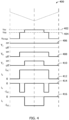
- FIG. 4 illustrates a high-efficiency switching sequence 400 for controlling CSR 100 (shown in FIG. 1 ).
- switching sequence 400 includes the voltage imposed by the rectifier bridge on to the DC-link (either line-line voltage 402 u AC measured between capacitors C i on phase lines A, C, or line-line voltage 404 u BC measured across capacitors C i on phase lines B, C, depending on switch state), switching state signals 406, 408, 410 for each of switches 112 T1, T6, T2, respectively, and input currents 412, 414, 416 i A , i B , i C .
- controller 130 is configured to lock one switch 112 from one of the first, second, and third phase legs A, B, C in an ON position, and commutate one switch 112 from each of the two remaining phase legs.
- switch 112 T1 is locked ON, while the other two switches 112 T2 and T6 are switched and commutated.
- controller 130 At least partially superimposes input voltages generated by the two commutated switches (i.e., switches 112 T2 and T6) as opposed to decoupling them. Controller 130 then determines which of the two commutated switches 112 T2 and T6 has a lower line-line voltage based on the measured input voltages, and performs all switching actions during the high-efficiency switching sequence based on the determined lower line-line voltage to facilitate operating CSR system 100 at a higher efficiency.
- the two commutated switches i.e., switches 112 T2 and T6
- controller 130 evaluates input capacitor voltage across capacitors C 12 , C 23 , C 31 . For the two active switches 112 T6 and T2, controller 130 determines the one with the highest line-to-line voltage and the one with the lowest line-to-line voltage.
- the high-efficiency modulation scheme improves efficiency by ensuring that all switching actions are performed with the minimal switched line-to-line voltage, while exposing freewheeling diode D f 124 to a single reverse-recovery event. Because switches 112 will be exposed to the lowest possible voltage, losses from freewheeling diode D f 124 are reduced and switching losses on the active switches are reduced.
- high-efficiency switching sequence 400 suffers from power quality degradation at the sliding intersection of the input filter capacitor voltages. Due to switching ripple on input filter capacitors 108 C i the voltages across capacitors C i intersect multiple times over a switching cycle, causing associated distortion on the input current.
- FIG. 5 illustrates an adaptive switching sequence 500 for use in controlling CSR 100 (shown in FIG. 1 ).
- CSR 100 is initially driven using high-efficiency switching sequence 400 (shown in FIG. 4 ).
- the line-line capacitor voltages across input capacitors C i are monitored by controller 130 (shown in FIG. 1 ). More specifically, controller 130 receives the measured input voltages from at least one sensor 136 coupled to the three phase lines A, B, C. Controller 130 determines whether the measured input voltages fall within a predetermined voltage range and selects which of the high-efficiency and high-quality switching sequences to apply to switches 112 T1 - T6 based on the determination.
- controller 130 When the voltages of the two active legs T6 and T2 approach an intersection point 502 (signaled by the line-line voltages approaching zero), controller 130 changes the switching sequence being applied from high-efficiency switching sequence 400 to high-quality switching sequence 300 (shown in FIG. 3 ).
- a predetermined voltage range 504 is defined in a memory of controller 130 using hysteresis. Predetermined voltage range 504 ensures correct selection of a switching sequence irrespective of ripple on capacitor voltage and/or line voltage distortion. After crossing intersection point 502 and exceeding predetermined voltage range 504, controller 130 changes the applied switching sequence back to high-efficiency switching sequence 400.
- high-quality switching sequence 300 is used when the line-line voltages are within the predetermined voltage range 504 range surrounding intersection point 502 to mitigate and/or reduce the current distortion.
- high-efficiency switching sequence 400 is applied to achieve the highestefficiency operation of CSR 100.
- FIG. 6 illustrates an adaptive switching sequence 600 for use in controlling CSR 100 (shown in FIG. 1 ).
- CSR 100 is initially driven using high-efficiency switching sequence 400 (shown in FIG. 4 ).
- the line-line capacitor voltages across input capacitors C i are monitored by controller 130 (shown in FIG. 1 ).
- controller 130 determines which switching sequence to apply, a predetermined voltage range 602 is defined in a memory of controller 130 using hysteresis. Controller 130 determines whether the measured input voltages fall within predetermined voltage range and selects which of the switching sequences to apply to switches 112 based on the outcome of the determination.
- Predetermined voltage range 602 ensures correct selection of a switching sequence irrespective of ripple on capacitor voltage and/or line voltage distortion.
- controller 130 determines which sector of a plurality of predefined sectors (shown in FIG. 2 ) the measured input voltages fall within. The determined sector indicates which of switches 112 are commutated during switching sequences 300, 400.
- controller 130 changes the switching sequence being applied from high-efficiency switching sequence 400 to an alternative high-quality switching sequence 606.
- alternative high-quality switching sequence 606 includes switching state signals 608, 610, 612 for each of switches 112 T1, T6, T2, respectively. Substantially, the pulse signals 610, 612 on active legs T6, T2 are not overlapping, in order to avoid the issues related to the voltage sliding intersection.
- Switching ripple on the capacitor voltage or distortion on the line voltage causes multiple consecutive sub-phase-sector changes to occur in the SVM analysis.
- Alternative high-quality switching sequence 606 mitigates the losses present near intersection point 604 by applying the non-overlapping pulse signals 610, 612 while the sub-phase-sector is locked.
- controller 130 After crossing intersection point 604 and exceeding predetermined voltage range 602, controller 130 changes the applied switching sequence back to high-efficiency switching sequence 400.
- CSR 100 may be used as a front-end rectifier in double conversion AC UPS applications. In another embodiment, CSR 100 may be used as a rectifying stage of DC UPS.
Landscapes
- Engineering & Computer Science (AREA)
- Power Engineering (AREA)
- Rectifiers (AREA)
Description
- The field of the invention relates generally to current source rectifiers (CSRs), and more particularly, to methods and control systems for controlling active rectifiers in CSR systems.
- CSRs are commonly used in a variety of applications, such as in uninterruptible power supplies (UPSs), telecommunication and data centers, electric motors, etc., because of their ability to operate the CSR at unity power factor with sinusoidal AC currents. At the same time, efficiency is a fundamental criterion that is considered during selection of a CSR system. Therefore, reduction of losses is an important factor for successful market adoption of current source conversion technology.
- There are two desirable, but competing, parameters associated with CSRs: high efficiency and low current distortion. Reducing switching losses by using some known modulation sequences introduces undesirable side effects in terms of input current distortion. Other known solutions, for example, increasing input filter capacitance or increasing the switching frequency, are not of practical use and may compromise cost/footprint or performance.
-
US 2015/0124505 (D1 ) discloses a three-phase current source rectifier (CSR) with three AC inputs. The CSR includes a controller, a free-wheeling diode with a cathode connected to a positive line and an anode connected to a negative line, three pairs of switches connected in parallel between the positive line and the negative line, and six pairs of diodes, each pair of the diodes being connected in series. Each two pairs of the diodes may be connected in parallel with each other and in series with a respective pair of switches. Each AC input may be connected to between each of two pairs of the diodes. - According to a first aspect of the invention, there is provided: a current source rectifier (CSR) system for a power source including three phase lines, the (CSR) system comprising: a rectifier operable to receive an alternating-current (AC) input voltage and provide a direct-current (DC) output voltage, the rectifier comprising: a first phase leg comprising first and second series-coupled switches coupled between a positive line and a negative line, wherein first and second diodes correspond with the first and second switches, and wherein a first node coupled to a first phase line of the three phase lines is directly connected between the first switch and a cathode end of the second diode; a second phase leg comprising third and fourth series-coupled switches coupled between the positive line and the negative line, wherein third and fourth diodes correspond with the third and fourth switches, and wherein a second node coupled to a second phase line of the three phase lines is directly connected between the third switch and a cathode end of the fourth diode; and a third phase leg comprising fifth and sixth series-coupled switches coupled between the positive line and the negative line, wherein fifth and sixth diodes correspond with the fifth and sixth switches, and wherein a third node coupled to a third phase line of the three phase lines is directly connected between the fifth switch and a cathode end of the sixth diode; and a controller communicatively coupled to the rectifier and operable to: define a predetermined voltage range in a memory of the controller by hysteresis; control operation of the switches in accordance with a first switching sequence when measured input voltages on at least two phase lines of the three phase lines are outside of the predetermined voltage range; and control operation of the switches in accordance with a second switching sequence when the measured input voltages on the at least two phase lines are within the predetermined voltage range.
-
-
FIG. 1 is a circuit diagram of an exemplary three-phase current source rectifier (CSR). -
FIG. 2 is a space vector diagram for controlling the CSR shown inFIG. 1 . -
FIG. 3 illustrates a high-quality switching sequence for controlling the CSR shown inFIG. 1 . -
FIG. 4 illustrates a high-efficiency switching sequence for controlling the CSR shown inFIG. 1 . -
FIG. 5 illustrates an adaptive switching sequence for use in controlling the CSR shown inFIG. 1 . -
FIG. 6 illustrates an alternative adaptive switching sequence for use in controlling the CSR shown inFIG. 1 . -
FIG. 1 is a circuit diagram of an exemplary three-phase current source rectifier (CSR) 100. As shown inFIG. 1 ,CSR 100 is a buck-type pulse-width-modulated (PWM) rectifier. -
CSR 100 is coupled to apower source 102 that generates three alternating current (AC) input voltages va, vb, and vc relative to a ground connection g. AC input voltages va, vb, and vc are provided toCSR 100 via three phase lines A, B, C, respectively. In the exemplary embodiment,power source 102 is a three-phase AC voltage source such as a grid or utility. However, in alternative embodiments,power source 102 may provide single-phase or multi-phase power toCSR 100. - CSR 100 includes an
input filter 104 coupled topower source 102.Input filter 104 includes an input filtering inductor 106 Li coupled on each phase line A, B, C and an input filter capacitor 108 Ci coupled between respective phase lines A, B, C and a mid-point node Ni. Input filter 104 is configured to prevent injection of high frequency switching harmonics byCSR 100. - In the exemplary embodiment, CSR 100 includes a
rectifier 110 coupled to an output side ofinput filter 104.Rectifier 110 is operable to receive an alternating current (AC) input voltage and generate a direct current (DC) output voltage.Rectifier 110 is an active switching-type CSR and includes six switches 112 (T1, T2, T3, T4, T5, T6) and six diodes 114 (D1, D2, D3, D4, D5, D6) series-coupled withswitches 112 T1 - T6, respectively, between apositive line 116 and anegative line 118. Switches T1, T4 and diodes D1, D4 form a first phase leg ofrectifier 110, which is coupled to phase line A for receiving input voltage va. Switches T3, T6 and diodes D3, D6 form a second phase leg ofrectifier 110, which is coupled to phase line B for receiving input voltage vb. Switches T5, T2 and diodes D5, D2 form a third phase leg ofrectifier 110, which is coupled to phase line C for receiving input voltage vc. Accordingly, each switch ofswitches 112 T1 - T6 is coupled to an associated phase line of the three phase lines A, B, C. In the exemplary embodiment,switches 112 T1 - T6 TO are silicon insulated-gate bipolar transistors (IGBTs). Alternatively,switches 112 T1 - T6 may include bipolar junction transistors (BJTs), metal-oxide-semiconductor field effect transistors (MOSFETs), junction field effect transistors (JFETs), Gate turn-off (GTO) thyristors, integrated gate-commutated thyristors (IGCTs) or the like. - A
DC link 120 is defined onpositive line 116 andnegative line 118 between an output ofrectifier 110 and aload 122, which may be an inverter. In the exemplary embodiment,DC link 120 includes afreewheeling diode D f 124, afilter inductor L DC 126, and a DClink capacitor C DC 128.Freewheeling diode D f 124 includes a cathode coupled topositive line 116 and an anode coupled tonegative line 118, and allows current to flow only fromnegative line 118 topositive line 116 throughfreewheeling diode D f 124. The presence offreewheeling diode D f 124 is optional, but when present, it operable to reduce conduction losses when regenerative capability is not necessary. - DC
link capacitor C DC 128 is also coupled topositive line 116 andnegative line 118, and is configured to filter or smooth the pulsed DC voltage output byrectifier 110.Filter inductor L DC 126 is coupled to bothpositive line 116 andnegative line 118 betweenfreewheeling diode D f 124 and DClink capacitor C DC 128. The filtered DC voltage is then provided to load 122. - A
controller 130 is communicatively coupled to each ofswitches 112 T1 - T6 and is operable to control operation ofswitches 112 T1 - T6 in accordance with switching sequences based on whether measured input voltages on at least two phase lines of the three phase lines A, B, C are inside or outside of a predetermined voltage range. In the exemplary embodiment, the first switching sequence is a high-efficiency switching sequence configured to improve efficiency ofCSR system 100 when the measured input voltages are outside the predetermined voltage range, and the second switching sequence is a high-quality switching sequence configured to reduce current distortion caused when the measured input voltages are within the predetermined voltage range. - In the exemplary embodiment,
controller 130 includes one or more processors and associated memory as well as I/O circuits including driver circuitry for generatingswitching control signals 132 S1 - S6 to selectively actuate switches T1 - T6, respectively.Controller 130 may be implemented as any suitable hardware, processor-executed software, processor-executed firmware, programmable logic, or combinations thereof, operative as any suitable controller or regulator by whichrectifier 110 is controlled according to one or more desired switching sequences. - During operation,
controller 130 providesswitching control signals 132 S1 - S6 for causingrectifier 110 to convert AC electrical input power to provide a regulated DC current IDC toDC link 120. In determining a switching sequence to apply,controller 130 may employ one or more feedback signals orvalues 134, such as phase voltages va, vb, and vc measured by at least onesensor 136 coupled across input filter capacitors 108 Ci and/or the DC link current IDC and/or DC link voltage. DC-link voltage sensing is typically required for regulation, as it is the controlled output of the converter. Additionally, the DC link current IDC may be used for current-limiting operations (e.g. battery recharge) and protection schemes (e.g. converter shutdown under load side fault). Further, in some embodiments, the DC link current IDC may be used as a feed-forward term in the converter control.Controller 130 may also implement other control functions such as power factor correction. -
FIG. 2 is a space vector diagram 200 for controlling CSR 100 (shown inFIG. 1 ). Space vector modulation (SVM) is a common strategy for driving CSRs. In the exemplary embodiment, space vector diagram 200 is provided in a Stationary Reference Frame (SRF) and includes six phase sectors. In each phase sector, a modulation vector is synthesized by combining two adjacent vectors and a zero vector (also referred to as a freewheeling vector). - At any given time, only two
switches 112 T1 - T6 may conduct: one on the upper half ofrectifier 110 and the other on the lower half ofrectifier 110. Detailed analysis shows that when synthesizing a current vector in a given phase sector, one switch 112 (e.g., T1) remains ON, while the two opposite switches 112 (e.g., T6 and T2) on the other two legs are commutated. The applied switching sequence affects the performance ofCSR 100. It should be noted that while this description focuses solely onswitches 112 T1, T6, and T2 (associated with vectors [12] and [61] inFIG. 2 ), a substantially similar analysis and procedure may be applicable to any and all other switch combinations, and their description will not be repeated herein. - Switching losses within
CSR 100 may be minimized by selecting an appropriate switching sequence. However, minimal switching loss strategies may exhibit undesirable side effects such as degradation of the input performance (mainly in terms of current distortion). -
FIG. 3 illustrates a high-quality switching sequence 300 for controlling CSR 100 (shown inFIG. 1 ).Switching sequence 300 includes the voltage imposed by the rectifier bridge onto the DC-link (either line-line voltage 302 u AC measured between capacitors Ci on phase lines A, C, or line-line voltage 304 u BC measured across capacitors Ci on phase lines B, C, depending on switch state), switchingstate signals switches 112 TR1, TR6, TR2, respectively, andinput currents - In the exemplary embodiment, to apply the high-
quality switching sequence 300,controller 130 generates symmetric switching pulses for the two commutatedswitches 112 T2 and T6 including afreewheeling state 318 following each of the symmetric switching pulses. Free-wheelingstates 318 occur where bothswitches 112 T2 and T6 are OFF. That is, a freewheeling vector is interposed between the vectors for theactive switches 112 T6, T2. Each leg is locked for 60° of the phase cycle time, and so eachswitch 112 T1 - T6 is on for 60° of the time. In the illustrated embodiment, switch 112 TI is locked ON, while the other twoswitches 112 T2 and T6 are switched and commutated. Additionally,controller 130 decouples the two commutatedswitches 112 T2 and T6 during thefreewheeling state 318 to improve a quality of the input power. Decoupling the two commutatedswitches 112 T2 and T6 during thefreewheeling state 318 reduces current distortion near intersections of two phases of the input voltage. Further, interposingfreewheeling sections 318 between pulses enables complete control of the sine wave that is going to be synthesized. This is referred to as a "high-quality" switching sequence because effectively the twoswitches 112 T2 and T6 are operating independently of one other. However, the "high-quality" switching sequence strategy is sub-optimal in terms of efficiency (particularly, in terms of switching losses) because each time aswitch 112 is turned ON, freewheelingdiode D f 124 turns ON, introducing switching losses. -
FIG. 4 illustrates a high-efficiency switching sequence 400 for controlling CSR 100 (shown inFIG. 1 ). Similarly to switchingsequence 300, switchingsequence 400 includes the voltage imposed by the rectifier bridge on to the DC-link (either line-line voltage 402 u AC measured between capacitors Ci on phase lines A, C, or line-line voltage 404 u BC measured across capacitors Ci on phase lines B, C, depending on switch state), switching state signals 406, 408, 410 for each ofswitches 112 T1, T6, T2, respectively, andinput currents - In the exemplary embodiment,
controller 130 is configured to lock oneswitch 112 from one of the first, second, and third phase legs A, B, C in an ON position, and commutate oneswitch 112 from each of the two remaining phase legs. For example, in one embodiment, switch 112 T1 is locked ON, while the other twoswitches 112 T2 and T6 are switched and commutated. - To apply the high-efficiency switching sequence,
controller 130 at least partially superimposes input voltages generated by the two commutated switches (i.e., switches 112 T2 and T6) as opposed to decoupling them.Controller 130 then determines which of the two commutatedswitches 112 T2 and T6 has a lower line-line voltage based on the measured input voltages, and performs all switching actions during the high-efficiency switching sequence based on the determined lower line-line voltage to facilitateoperating CSR system 100 at a higher efficiency. - To apply high-
efficiency switching sequence 400,controller 130 evaluates input capacitor voltage across capacitors C12, C23, C31. For the twoactive switches 112 T6 and T2,controller 130 determines the one with the highest line-to-line voltage and the one with the lowest line-to-line voltage. - The high-efficiency modulation scheme improves efficiency by ensuring that all switching actions are performed with the minimal switched line-to-line voltage, while exposing
freewheeling diode D f 124 to a single reverse-recovery event. Becauseswitches 112 will be exposed to the lowest possible voltage, losses from freewheelingdiode D f 124 are reduced and switching losses on the active switches are reduced. - However, high-
efficiency switching sequence 400 suffers from power quality degradation at the sliding intersection of the input filter capacitor voltages. Due to switching ripple on input filter capacitors 108 Ci the voltages across capacitors Ci intersect multiple times over a switching cycle, causing associated distortion on the input current. -
FIG. 5 illustrates anadaptive switching sequence 500 for use in controlling CSR 100 (shown inFIG. 1 ).CSR 100 is initially driven using high-efficiency switching sequence 400 (shown inFIG. 4 ). The line-line capacitor voltages across input capacitors Ci are monitored by controller 130 (shown inFIG. 1 ). More specifically,controller 130 receives the measured input voltages from at least onesensor 136 coupled to the three phase lines A, B,C. Controller 130 determines whether the measured input voltages fall within a predetermined voltage range and selects which of the high-efficiency and high-quality switching sequences to apply toswitches 112 T1 - T6 based on the determination. - When the voltages of the two active legs T6 and T2 approach an intersection point 502 (signaled by the line-line voltages approaching zero),
controller 130 changes the switching sequence being applied from high-efficiency switching sequence 400 to high-quality switching sequence 300 (shown inFIG. 3 ). To enablecontroller 130 to determine when to change the switching sequence, apredetermined voltage range 504 is defined in a memory ofcontroller 130 using hysteresis.Predetermined voltage range 504 ensures correct selection of a switching sequence irrespective of ripple on capacitor voltage and/or line voltage distortion. After crossingintersection point 502 and exceedingpredetermined voltage range 504,controller 130 changes the applied switching sequence back to high-efficiency switching sequence 400. - Because current distortion is only significantly introduced near intersection points of input voltages va, vb, and vc, high-
quality switching sequence 300 is used when the line-line voltages are within thepredetermined voltage range 504 range surroundingintersection point 502 to mitigate and/or reduce the current distortion. When the line-line voltages are not within thepredetermined voltage range 504, high-efficiency switching sequence 400 is applied to achieve the highestefficiency operation ofCSR 100. By using a combination of high-efficiency and high-quality switching sequences adaptive switching sequence 500 facilitates capitalizing on the efficiency benefits from reduced switching losses while mitigating side effects, thereby preserving (or even improving) the high power-factor/low-distortion input characteristics ofCSR 100. -
FIG. 6 illustrates anadaptive switching sequence 600 for use in controlling CSR 100 (shown inFIG. 1 ).CSR 100 is initially driven using high-efficiency switching sequence 400 (shown inFIG. 4 ). The line-line capacitor voltages across input capacitors Ci are monitored by controller 130 (shown inFIG. 1 ). To enablecontroller 130 to determine which switching sequence to apply, apredetermined voltage range 602 is defined in a memory ofcontroller 130 using hysteresis.Controller 130 determines whether the measured input voltages fall within predetermined voltage range and selects which of the switching sequences to apply toswitches 112 based on the outcome of the determination.Predetermined voltage range 602 ensures correct selection of a switching sequence irrespective of ripple on capacitor voltage and/or line voltage distortion. Additionally,controller 130 determines which sector of a plurality of predefined sectors (shown inFIG. 2 ) the measured input voltages fall within. The determined sector indicates which ofswitches 112 are commutated during switchingsequences - When the voltages of the two active legs T6 and T2 approach an intersection point 604 (signaled by the line-line voltages approaching zero),
controller 130 changes the switching sequence being applied from high-efficiency switching sequence 400 to an alternative high-quality switching sequence 606. - In the exemplary embodiment, alternative high-
quality switching sequence 606 includes switching state signals 608, 610, 612 for each ofswitches 112 T1, T6, T2, respectively. Substantially, the pulse signals 610, 612 on active legs T6, T2 are not overlapping, in order to avoid the issues related to the voltage sliding intersection. - Switching ripple on the capacitor voltage or distortion on the line voltage causes multiple consecutive sub-phase-sector changes to occur in the SVM analysis. Alternative high-
quality switching sequence 606 mitigates the losses present nearintersection point 604 by applying the non-overlapping pulse signals 610, 612 while the sub-phase-sector is locked. - After crossing
intersection point 604 and exceedingpredetermined voltage range 602,controller 130 changes the applied switching sequence back to high-efficiency switching sequence 400. - In one embodiment,
CSR 100 may be used as a front-end rectifier in double conversion AC UPS applications. In another embodiment,CSR 100 may be used as a rectifying stage of DC UPS. - Additionally, alternative topologies performing as a current source at the input (e.g. matrix converters) may also benefit (to some extent) from the disclosed invention.
Claims (15)
- A current source rectifier, CSR, system (100) for a power source including three phase lines (A, B, C), the CSR system comprising:a rectifier (110) operable to receive an alternating-current, AC, input voltage and provide a direct-current, DC, output voltage, the rectifier comprising:a first phase leg comprising first and second series-coupled switches coupled between a positive line (116) and a negative line (118), wherein first and second diodes correspond with the first and second switches, and wherein a first node coupled to a first phase line of the three phase lines is directly connected between the first switch and a cathode end of the second diode;a second phase leg comprising third and fourth series-coupled switches coupled between the positive line and the negative line, wherein third and fourth diodes correspond with the third and fourth switches, and wherein a second node coupled to a second phase line of the three phase lines is directly connected between the third switch and a cathode end of the fourth diode; anda third phase leg comprising fifth and sixth series-coupled switches coupled between the positive line and the negative line, wherein fifth and sixth diodes correspond with the fifth and sixth switches, and wherein a third node coupled to a third phase line of the three phase lines is directly connected between the fifth switch and a cathode end of the sixth diode; anda controller (130) communicatively coupled to the rectifier and operable to:define a predetermined voltage range in a memory of the controller by hysteresis;control operation of the switches in accordance with a first switching sequence (400) when measured input voltages on at least two phase lines of the three phase lines are outside of the predetermined voltage range; andcontrol operation of the switches in accordance with a second switching sequence (300) when the measured input voltages on the at least two phase lines are within the predetermined voltage range.
- The current source rectifier system in accordance with Claim 1, wherein the first switching sequence is a switching sequence configured to improve efficiency of the current source rectifier system when the measured input voltages are outside the predetermined voltage range (504, 602).
- The current source rectifier system in accordance with Claim 1 or Claim 2, wherein the second switching sequence is a switching sequence configured to reduce current distortion caused when the measured input voltages are within the predetermined voltage range.
- The current source rectifier system in accordance with any preceding Claim, wherein the controller is further configured to:receive the measured input voltages from at least one sensor coupled to the three phase lines;determine whether the measured input voltages fall within the predetermined voltage range; andselect which of the first and second switching sequences to apply to the switches based on the determination.
- The current source rectifier system in accordance with any preceding Claim, wherein the measured input voltages are associated with a sector of a plurality of predefined sectors in a space vector diagram, and wherein the controller is further configured to:determine which sector the measured input voltages fall within; anddetermine which switches to commutate based on the determined sector.
- The current source rectifier system in accordance with any preceding Claim, wherein to control operation of the switches in accordance with the first and second switching sequences, the controller is further configured to generate and transmit control signals (132) to selectively turn each respective switch ON and OFF.
- The current source rectifier system in accordance with Claim 6, wherein to generate the control signals, the controller is configured to use space vector modulation.
- The current source rectifier system in accordance with any preceding claim, wherein, the controller is configured to:lock one switch from one of the first, second, and third phase legs in an ON position for the duration of the switching sequence used to control operation of the switches; andcommutate one switch from each of the two remaining phase legs.
- The current source rectifier system in accordance with Claim 8, wherein to apply the first switching sequence, the controller is configured to:at least partially superimpose input voltages resulting from the operation of the the two commutated switches; determine which of the two commutated switches has a lower line-line voltage based on the measured input voltages; andperform all switching actions during the first switching sequence based on the determined lower line-line voltage to facilitate operating the current source rectifier system at a higher efficiency.
- The current source rectifier system in accordance with Claim 8 or Claim 9, wherein to apply the second switching sequence, the controller is configured to:generate symmetric switching pulses for the two commutated switches including a freewheeling state (318) following each of the symmetric switching pulses; anddecouple the two commutated switches during the freewheeling state to improve a quality of the input power.
- The current source rectifier system in accordance with Claim 10, wherein decoupling the two commutated switches during the freewheeling state reduces current distortion near intersections of two phases of the input voltage.
- The current source rectifier system in accordance with any preceding Claim, wherein the controller is configured to:control operation of the switches in accordance with the first switching sequence to improve efficiency of the current source rectifier system by reducing switching losses; andcontrol operation of the switches in accordance with the second switching sequence as the measured input voltages converge towards an intersection point to reduce current distortion and improve quality of the power signals.
- The current source rectifier system in accordance with any preceding Claim, wherein the controller is further configured to select the second switching sequence from among a plurality of switching sequences configured to reduce current distortion when the measured input voltages on the at least two phase lines are within the predetermined voltage range.
- The current source rectifier system in accordance with any preceding Claim, wherein the controller is further configured to operate the plurality of switches in accordance with an adaptive switching sequence comprising the first and second switching sequences.
- The current source rectifier system in accordance with claim 14, wherein the adaptive switching sequence operates to apply the first and second switching sequences to facilitate efficiency benefits of reduced switching losses from the first switching sequence while from the second switching sequence maintaining high power-factor and low-distortion input characteristics of the CSR system.
Applications Claiming Priority (2)
| Application Number | Priority Date | Filing Date | Title |
|---|---|---|---|
| US15/955,077 US10574136B2 (en) | 2018-04-17 | 2018-04-17 | Methods and systems for controlling current source rectifiers |
| PCT/EP2019/059924 WO2019201993A1 (en) | 2018-04-17 | 2019-04-17 | Methods and systems for controlling current source rectifiers |
Publications (2)
| Publication Number | Publication Date |
|---|---|
| EP3782273A1 EP3782273A1 (en) | 2021-02-24 |
| EP3782273B1 true EP3782273B1 (en) | 2025-01-15 |
Family
ID=66240136
Family Applications (1)
| Application Number | Title | Priority Date | Filing Date |
|---|---|---|---|
| EP19718681.0A Active EP3782273B1 (en) | 2018-04-17 | 2019-04-17 | Methods and systems for controlling current source rectifiers |
Country Status (3)
| Country | Link |
|---|---|
| US (2) | US10574136B2 (en) |
| EP (1) | EP3782273B1 (en) |
| WO (1) | WO2019201993A1 (en) |
Families Citing this family (9)
| Publication number | Priority date | Publication date | Assignee | Title |
|---|---|---|---|---|
| US10574136B2 (en) | 2018-04-17 | 2020-02-25 | Abb Schweiz Ag | Methods and systems for controlling current source rectifiers |
| EP3726719A1 (en) * | 2019-04-15 | 2020-10-21 | Infineon Technologies Austria AG | Power converter and power conversion method |
| JP7377745B2 (en) * | 2020-03-05 | 2023-11-10 | 株式会社日立製作所 | power converter |
| KR102815721B1 (en) * | 2020-04-29 | 2025-06-02 | 삼성전자주식회사 | Power supply system including thyristor and method for a controlling the power supply system |
| CN111674275A (en) | 2020-06-18 | 2020-09-18 | 薛洛良 | DC charging system for electric vehicle using transformer output voltage of 1250 volts |
| US12255550B2 (en) * | 2021-03-12 | 2025-03-18 | Wisconsin Alumni Research Foundation | Current source inverter using bidirectional switches with bidirectional power flow capability |
| CN114244159B (en) * | 2021-12-21 | 2025-11-07 | 薛洛良 | Energy-saving control method of CSR high-frequency PWM rectification circuit |
| CN114583988A (en) * | 2022-03-09 | 2022-06-03 | 薛洛良 | Parallel method of output-to-ground balance of CSR high-frequency PWM rectifier circuit |
| CN116505785B (en) * | 2023-06-21 | 2023-09-05 | 合肥工业大学 | Current-type PWM rectifier and control strategy thereof |
Citations (1)
| Publication number | Priority date | Publication date | Assignee | Title |
|---|---|---|---|---|
| US20140268934A1 (en) * | 2013-03-12 | 2014-09-18 | University Of Tennessee Research Foundation | Three-phase buck rectifier for power supplies |
Family Cites Families (16)
| Publication number | Priority date | Publication date | Assignee | Title |
|---|---|---|---|---|
| US5345375A (en) * | 1991-12-16 | 1994-09-06 | Regents Of The University Of Minnesota | System and method for reducing harmonic currents by current injection |
| US7768805B2 (en) * | 2007-03-09 | 2010-08-03 | General Electric Company | Clean input UPS with fast rectifier control and improved battery life |
| US8223511B2 (en) | 2010-06-07 | 2012-07-17 | Rockwell Automation Technologies, Inc. | Common mode voltage reduction apparatus and method for current source converter based drive |
| JP5459304B2 (en) | 2011-02-28 | 2014-04-02 | 株式会社安川電機 | Current source power converter |
| US8513904B2 (en) * | 2011-11-17 | 2013-08-20 | Micrel, Inc. | Step-down hysteretic current LED driver implementing frequency regulation |
| JP5549697B2 (en) | 2012-03-02 | 2014-07-16 | 株式会社安川電機 | Current source power converter |
| US9240732B2 (en) * | 2012-05-22 | 2016-01-19 | Drs Power & Control Technologies, Inc. | Harmonic regulator for current source rectification and inversion |
| US8873261B1 (en) | 2013-05-09 | 2014-10-28 | Drs Power & Control Technologies, Inc. | Current source rectifier modulation in discontinuous modes of operation |
| US9774246B2 (en) | 2013-10-11 | 2017-09-26 | University Of Tennessee Research Foundation | Three-phase current source rectifier for power supplies |
| US20150171663A1 (en) | 2013-12-18 | 2015-06-18 | Eaton Corporation | Uninterruptible power systems using current source rectifiers and methods of operating the same |
| WO2016024223A1 (en) * | 2014-08-13 | 2016-02-18 | Inesc Porto- Instituto De Engenharia De Sistemas E Computadores Do Porto | Ac/dc converter with three to single phase matrix converter, full-bridge ac/dc converter and hf transformer |
| US10103643B2 (en) | 2014-10-28 | 2018-10-16 | Murata Manufacturing Co., Ltd. | Space vector modulation for matrix converter and current source converter |
| US10027112B2 (en) * | 2015-06-24 | 2018-07-17 | Eaton Intelligent Power Limited | High voltage power supplies using serially coupled current source rectifiers and methods of operating the same |
| WO2017049250A1 (en) * | 2015-09-18 | 2017-03-23 | Murata Manufacturing Co., Ltd. | Pwm scheme based on space vector modulation for three-phase rectifier converters |
| US10574136B2 (en) | 2018-04-17 | 2020-02-25 | Abb Schweiz Ag | Methods and systems for controlling current source rectifiers |
| CN110120752B (en) * | 2018-02-05 | 2021-04-27 | 台达电子企业管理(上海)有限公司 | Power converter and control method thereof |
-
2018
- 2018-04-17 US US15/955,077 patent/US10574136B2/en active Active
-
2019
- 2019-04-17 WO PCT/EP2019/059924 patent/WO2019201993A1/en not_active Ceased
- 2019-04-17 EP EP19718681.0A patent/EP3782273B1/en active Active
-
2020
- 2020-02-25 US US16/800,279 patent/US11205952B2/en active Active
Patent Citations (1)
| Publication number | Priority date | Publication date | Assignee | Title |
|---|---|---|---|---|
| US20140268934A1 (en) * | 2013-03-12 | 2014-09-18 | University Of Tennessee Research Foundation | Three-phase buck rectifier for power supplies |
Also Published As
| Publication number | Publication date |
|---|---|
| US20200195130A1 (en) | 2020-06-18 |
| WO2019201993A1 (en) | 2019-10-24 |
| US20190319546A1 (en) | 2019-10-17 |
| WO2019201993A9 (en) | 2019-12-12 |
| US10574136B2 (en) | 2020-02-25 |
| US11205952B2 (en) | 2021-12-21 |
| EP3782273A1 (en) | 2021-02-24 |
Similar Documents
| Publication | Publication Date | Title |
|---|---|---|
| EP3782273B1 (en) | Methods and systems for controlling current source rectifiers | |
| EP3657661B1 (en) | Conversion circuit, control method, and power supply device | |
| US9325252B2 (en) | Multilevel converter systems and sinusoidal pulse width modulation methods | |
| KR101366393B1 (en) | 3-stage pulse width modulation inverter with discharge network | |
| US7881081B1 (en) | Systems and methods for reducing AC drive common-mode currents | |
| US10218285B2 (en) | Medium voltage hybrid multilevel converter and method for controlling a medium voltage hybrid multilevel converter | |
| EP2477304A1 (en) | Method and apparatus for generating a charging circuit | |
| Edpuganti et al. | Optimal low switching frequency pulsewidth modulation of nine-level cascade inverter | |
| JPH04197097A (en) | High capacity speed varying system for ac motor | |
| EP3151412B1 (en) | Power conversion device and three-phase ac power supply device | |
| Bak et al. | Reducing switching losses in indirect matrix converter drives: discontinuous PWM method | |
| Teixeira et al. | Topologically reduced multilevel converters using complementary unidirectional phase-legs | |
| EP3665766A1 (en) | Control of delta-connected converter | |
| US20240333124A1 (en) | Balancer Circuit for Series Connection of Two DC-Link Capacitors, Method for Controlling the Balancer Circuit and Converter Arrangement | |
| JP2009095159A (en) | Power converter | |
| US20200328693A1 (en) | Converter circuit, power conversion system, and motor drive apparatus | |
| US20240178739A1 (en) | Control apparatus for an arcp inverter | |
| KR20140119164A (en) | Elective control of an alternating current motor or direct current motor | |
| KR101520899B1 (en) | Three-phase pwm converter system reducing resonance effect | |
| Somani et al. | Circulating currents in open-end winding PWM ac drives | |
| EP4344036A1 (en) | Active filter pre-charging for a converter with active filter cells | |
| Vafakhah et al. | Space-vector PWM for inverters with split-wound coupled inductors | |
| Zhang et al. | Current source converter with switched-inductor DC link circuit for reduced converter losses | |
| CN118631029B (en) | Multi-phase full-bridge drive system and method for driving a motor | |
| Park et al. | A Z-source sparse matrix converter under a voltage sag condition |
Legal Events
| Date | Code | Title | Description |
|---|---|---|---|
| STAA | Information on the status of an ep patent application or granted ep patent |
Free format text: STATUS: UNKNOWN |
|
| STAA | Information on the status of an ep patent application or granted ep patent |
Free format text: STATUS: THE INTERNATIONAL PUBLICATION HAS BEEN MADE |
|
| PUAI | Public reference made under article 153(3) epc to a published international application that has entered the european phase |
Free format text: ORIGINAL CODE: 0009012 |
|
| STAA | Information on the status of an ep patent application or granted ep patent |
Free format text: STATUS: REQUEST FOR EXAMINATION WAS MADE |
|
| 17P | Request for examination filed |
Effective date: 20200914 |
|
| AK | Designated contracting states |
Kind code of ref document: A1 Designated state(s): AL AT BE BG CH CY CZ DE DK EE ES FI FR GB GR HR HU IE IS IT LI LT LU LV MC MK MT NL NO PL PT RO RS SE SI SK SM TR |
|
| AX | Request for extension of the european patent |
Extension state: BA ME |
|
| RAP3 | Party data changed (applicant data changed or rights of an application transferred) |
Owner name: ABB SCHWEIZ AG |
|
| DAV | Request for validation of the european patent (deleted) | ||
| DAX | Request for extension of the european patent (deleted) | ||
| GRAP | Despatch of communication of intention to grant a patent |
Free format text: ORIGINAL CODE: EPIDOSNIGR1 |
|
| STAA | Information on the status of an ep patent application or granted ep patent |
Free format text: STATUS: GRANT OF PATENT IS INTENDED |
|
| INTG | Intention to grant announced |
Effective date: 20240808 |
|
| GRAS | Grant fee paid |
Free format text: ORIGINAL CODE: EPIDOSNIGR3 |
|
| GRAA | (expected) grant |
Free format text: ORIGINAL CODE: 0009210 |
|
| STAA | Information on the status of an ep patent application or granted ep patent |
Free format text: STATUS: THE PATENT HAS BEEN GRANTED |
|
| AK | Designated contracting states |
Kind code of ref document: B1 Designated state(s): AL AT BE BG CH CY CZ DE DK EE ES FI FR GB GR HR HU IE IS IT LI LT LU LV MC MK MT NL NO PL PT RO RS SE SI SK SM TR |
|
| REG | Reference to a national code |
Ref country code: CH Ref legal event code: EP Ref country code: GB Ref legal event code: FG4D |
|
| REG | Reference to a national code |
Ref country code: DE Ref legal event code: R096 Ref document number: 602019064846 Country of ref document: DE |
|
| REG | Reference to a national code |
Ref country code: IE Ref legal event code: FG4D |
|
| REG | Reference to a national code |
Ref country code: NL Ref legal event code: MP Effective date: 20250115 |
|
| PG25 | Lapsed in a contracting state [announced via postgrant information from national office to epo] |
Ref country code: NL Free format text: LAPSE BECAUSE OF FAILURE TO SUBMIT A TRANSLATION OF THE DESCRIPTION OR TO PAY THE FEE WITHIN THE PRESCRIBED TIME-LIMIT Effective date: 20250115 |
|
| PG25 | Lapsed in a contracting state [announced via postgrant information from national office to epo] |
Ref country code: RS Free format text: LAPSE BECAUSE OF FAILURE TO SUBMIT A TRANSLATION OF THE DESCRIPTION OR TO PAY THE FEE WITHIN THE PRESCRIBED TIME-LIMIT Effective date: 20250415 |
|
| PG25 | Lapsed in a contracting state [announced via postgrant information from national office to epo] |
Ref country code: FI Free format text: LAPSE BECAUSE OF FAILURE TO SUBMIT A TRANSLATION OF THE DESCRIPTION OR TO PAY THE FEE WITHIN THE PRESCRIBED TIME-LIMIT Effective date: 20250115 |
|
| PG25 | Lapsed in a contracting state [announced via postgrant information from national office to epo] |
Ref country code: PL Free format text: LAPSE BECAUSE OF FAILURE TO SUBMIT A TRANSLATION OF THE DESCRIPTION OR TO PAY THE FEE WITHIN THE PRESCRIBED TIME-LIMIT Effective date: 20250115 |
|
| PGFP | Annual fee paid to national office [announced via postgrant information from national office to epo] |
Ref country code: DE Payment date: 20250422 Year of fee payment: 7 |
|
| PG25 | Lapsed in a contracting state [announced via postgrant information from national office to epo] |
Ref country code: ES Free format text: LAPSE BECAUSE OF FAILURE TO SUBMIT A TRANSLATION OF THE DESCRIPTION OR TO PAY THE FEE WITHIN THE PRESCRIBED TIME-LIMIT Effective date: 20250115 |
|
| REG | Reference to a national code |
Ref country code: LT Ref legal event code: MG9D |
|
| PG25 | Lapsed in a contracting state [announced via postgrant information from national office to epo] |
Ref country code: IS Free format text: LAPSE BECAUSE OF FAILURE TO SUBMIT A TRANSLATION OF THE DESCRIPTION OR TO PAY THE FEE WITHIN THE PRESCRIBED TIME-LIMIT Effective date: 20250515 Ref country code: NO Free format text: LAPSE BECAUSE OF FAILURE TO SUBMIT A TRANSLATION OF THE DESCRIPTION OR TO PAY THE FEE WITHIN THE PRESCRIBED TIME-LIMIT Effective date: 20250415 |
|
| PGFP | Annual fee paid to national office [announced via postgrant information from national office to epo] |
Ref country code: IT Payment date: 20250429 Year of fee payment: 7 |
|
| REG | Reference to a national code |
Ref country code: AT Ref legal event code: MK05 Ref document number: 1760479 Country of ref document: AT Kind code of ref document: T Effective date: 20250115 |
|
| PG25 | Lapsed in a contracting state [announced via postgrant information from national office to epo] |
Ref country code: HR Free format text: LAPSE BECAUSE OF FAILURE TO SUBMIT A TRANSLATION OF THE DESCRIPTION OR TO PAY THE FEE WITHIN THE PRESCRIBED TIME-LIMIT Effective date: 20250115 |
|
| PG25 | Lapsed in a contracting state [announced via postgrant information from national office to epo] |
Ref country code: LV Free format text: LAPSE BECAUSE OF FAILURE TO SUBMIT A TRANSLATION OF THE DESCRIPTION OR TO PAY THE FEE WITHIN THE PRESCRIBED TIME-LIMIT Effective date: 20250115 Ref country code: PT Free format text: LAPSE BECAUSE OF FAILURE TO SUBMIT A TRANSLATION OF THE DESCRIPTION OR TO PAY THE FEE WITHIN THE PRESCRIBED TIME-LIMIT Effective date: 20250515 |
|
| PGFP | Annual fee paid to national office [announced via postgrant information from national office to epo] |
Ref country code: FR Payment date: 20250425 Year of fee payment: 7 |
|
| PG25 | Lapsed in a contracting state [announced via postgrant information from national office to epo] |
Ref country code: BG Free format text: LAPSE BECAUSE OF FAILURE TO SUBMIT A TRANSLATION OF THE DESCRIPTION OR TO PAY THE FEE WITHIN THE PRESCRIBED TIME-LIMIT Effective date: 20250115 Ref country code: GR Free format text: LAPSE BECAUSE OF FAILURE TO SUBMIT A TRANSLATION OF THE DESCRIPTION OR TO PAY THE FEE WITHIN THE PRESCRIBED TIME-LIMIT Effective date: 20250416 |
|
| PG25 | Lapsed in a contracting state [announced via postgrant information from national office to epo] |
Ref country code: AT Free format text: LAPSE BECAUSE OF FAILURE TO SUBMIT A TRANSLATION OF THE DESCRIPTION OR TO PAY THE FEE WITHIN THE PRESCRIBED TIME-LIMIT Effective date: 20250115 |
|
| PG25 | Lapsed in a contracting state [announced via postgrant information from national office to epo] |
Ref country code: SE Free format text: LAPSE BECAUSE OF FAILURE TO SUBMIT A TRANSLATION OF THE DESCRIPTION OR TO PAY THE FEE WITHIN THE PRESCRIBED TIME-LIMIT Effective date: 20250115 |
|
| PG25 | Lapsed in a contracting state [announced via postgrant information from national office to epo] |
Ref country code: SM Free format text: LAPSE BECAUSE OF FAILURE TO SUBMIT A TRANSLATION OF THE DESCRIPTION OR TO PAY THE FEE WITHIN THE PRESCRIBED TIME-LIMIT Effective date: 20250115 |
|
| PG25 | Lapsed in a contracting state [announced via postgrant information from national office to epo] |
Ref country code: DK Free format text: LAPSE BECAUSE OF FAILURE TO SUBMIT A TRANSLATION OF THE DESCRIPTION OR TO PAY THE FEE WITHIN THE PRESCRIBED TIME-LIMIT Effective date: 20250115 |
|
| REG | Reference to a national code |
Ref country code: DE Ref legal event code: R097 Ref document number: 602019064846 Country of ref document: DE |
|
| PG25 | Lapsed in a contracting state [announced via postgrant information from national office to epo] |
Ref country code: EE Free format text: LAPSE BECAUSE OF FAILURE TO SUBMIT A TRANSLATION OF THE DESCRIPTION OR TO PAY THE FEE WITHIN THE PRESCRIBED TIME-LIMIT Effective date: 20250115 Ref country code: CZ Free format text: LAPSE BECAUSE OF FAILURE TO SUBMIT A TRANSLATION OF THE DESCRIPTION OR TO PAY THE FEE WITHIN THE PRESCRIBED TIME-LIMIT Effective date: 20250115 |
|
| PG25 | Lapsed in a contracting state [announced via postgrant information from national office to epo] |
Ref country code: RO Free format text: LAPSE BECAUSE OF FAILURE TO SUBMIT A TRANSLATION OF THE DESCRIPTION OR TO PAY THE FEE WITHIN THE PRESCRIBED TIME-LIMIT Effective date: 20250115 |
|
| PG25 | Lapsed in a contracting state [announced via postgrant information from national office to epo] |
Ref country code: SK Free format text: LAPSE BECAUSE OF FAILURE TO SUBMIT A TRANSLATION OF THE DESCRIPTION OR TO PAY THE FEE WITHIN THE PRESCRIBED TIME-LIMIT Effective date: 20250115 |
|
| PLBE | No opposition filed within time limit |
Free format text: ORIGINAL CODE: 0009261 |
|
| STAA | Information on the status of an ep patent application or granted ep patent |
Free format text: STATUS: NO OPPOSITION FILED WITHIN TIME LIMIT |
|
| REG | Reference to a national code |
Ref country code: CH Ref legal event code: H13 Free format text: ST27 STATUS EVENT CODE: U-0-0-H10-H13 (AS PROVIDED BY THE NATIONAL OFFICE) Effective date: 20251125 |
|
| REG | Reference to a national code |
Ref country code: CH Ref legal event code: L10 Free format text: ST27 STATUS EVENT CODE: U-0-0-L10-L00 (AS PROVIDED BY THE NATIONAL OFFICE) Effective date: 20251126 |
|
| PG25 | Lapsed in a contracting state [announced via postgrant information from national office to epo] |
Ref country code: LU Free format text: LAPSE BECAUSE OF NON-PAYMENT OF DUE FEES Effective date: 20250417 |
|
| PG25 | Lapsed in a contracting state [announced via postgrant information from national office to epo] |
Ref country code: MC Free format text: LAPSE BECAUSE OF FAILURE TO SUBMIT A TRANSLATION OF THE DESCRIPTION OR TO PAY THE FEE WITHIN THE PRESCRIBED TIME-LIMIT Effective date: 20250115 |
|
| 26N | No opposition filed |
Effective date: 20251016 |
|
| GBPC | Gb: european patent ceased through non-payment of renewal fee |
Effective date: 20250417 |
|
| REG | Reference to a national code |
Ref country code: BE Ref legal event code: MM Effective date: 20250430 |
|
| PG25 | Lapsed in a contracting state [announced via postgrant information from national office to epo] |
Ref country code: GB Free format text: LAPSE BECAUSE OF NON-PAYMENT OF DUE FEES Effective date: 20250417 |
|
| PG25 | Lapsed in a contracting state [announced via postgrant information from national office to epo] |
Ref country code: BE Free format text: LAPSE BECAUSE OF NON-PAYMENT OF DUE FEES Effective date: 20250430 |
|
| PG25 | Lapsed in a contracting state [announced via postgrant information from national office to epo] |
Ref country code: CH Free format text: LAPSE BECAUSE OF NON-PAYMENT OF DUE FEES Effective date: 20250430 |