EP3780908A1 - Dielectric heating device and dielectric heating electrode - Google Patents
Dielectric heating device and dielectric heating electrode Download PDFInfo
- Publication number
- EP3780908A1 EP3780908A1 EP18919096.0A EP18919096A EP3780908A1 EP 3780908 A1 EP3780908 A1 EP 3780908A1 EP 18919096 A EP18919096 A EP 18919096A EP 3780908 A1 EP3780908 A1 EP 3780908A1
- Authority
- EP
- European Patent Office
- Prior art keywords
- electrode
- electrodes
- dielectric heating
- heating device
- signal source
- Prior art date
- Legal status (The legal status is an assumption and is not a legal conclusion. Google has not performed a legal analysis and makes no representation as to the accuracy of the status listed.)
- Granted
Links
Images




Classifications
-
- H—ELECTRICITY
- H05—ELECTRIC TECHNIQUES NOT OTHERWISE PROVIDED FOR
- H05B—ELECTRIC HEATING; ELECTRIC LIGHT SOURCES NOT OTHERWISE PROVIDED FOR; CIRCUIT ARRANGEMENTS FOR ELECTRIC LIGHT SOURCES, IN GENERAL
- H05B6/00—Heating by electric, magnetic or electromagnetic fields
- H05B6/46—Dielectric heating
- H05B6/62—Apparatus for specific applications
-
- H—ELECTRICITY
- H05—ELECTRIC TECHNIQUES NOT OTHERWISE PROVIDED FOR
- H05B—ELECTRIC HEATING; ELECTRIC LIGHT SOURCES NOT OTHERWISE PROVIDED FOR; CIRCUIT ARRANGEMENTS FOR ELECTRIC LIGHT SOURCES, IN GENERAL
- H05B6/00—Heating by electric, magnetic or electromagnetic fields
- H05B6/46—Dielectric heating
- H05B6/54—Electrodes
-
- H—ELECTRICITY
- H05—ELECTRIC TECHNIQUES NOT OTHERWISE PROVIDED FOR
- H05B—ELECTRIC HEATING; ELECTRIC LIGHT SOURCES NOT OTHERWISE PROVIDED FOR; CIRCUIT ARRANGEMENTS FOR ELECTRIC LIGHT SOURCES, IN GENERAL
- H05B6/00—Heating by electric, magnetic or electromagnetic fields
- H05B6/46—Dielectric heating
- H05B6/48—Circuits
Definitions
- the present invention relates to a dielectric heating device for sandwiching a heating target between electrodes to heat that target, and dielectric heating electrodes therefor.
- a dielectric heating device such a method is employed in which, using two or more electrodes, a heating target is sandwiched therebetween and then, using a signal source, a voltage is applied across the electrodes, thereby heating the heating target.
- a high-frequency dielectric heating device which is a device for placing a heating target between opposite electrodes, thereby heating the target, and as for at least one of the electrodes, includes a deformable electrode that has a heat-insulative member and an electrically-conductive film formed on the external surface of the heat-insulative member and that may abut on the heating target.
- the high-frequency dielectric heating device can heat the heating target uniformly and in a short time, and suppress local temperature elevation inside and on the surface of the heating target.
- Patent Literature 1 Japanese Patent Application Laid-open No. 2011-61753
- This invention has been made to solve the problems as described above, and an object thereof is, in a small-size dielectric heating device, to suppress reduction of the heating efficiency for the heating target and to prevent components of the dielectric heating device from reaching a high-temperature state.
- a dielectric heating device comprises: two or more electrodes; a grounded surface connected to one of the electrodes; a signal source that is connected to one of the electrodes other than the electrode connected to the grounded surface, to output a high-frequency signal; a first element that is interposed serially between the signal source and the electrode connected to the signal source, to cause the high-frequency signal outputted from the signal source to pass through the first element, by using electric coupling or magnetic coupling between two terminals in the first element, the two terminals being not connected to each other by metal; and a second element that is interposed serially between the grounded surface and the electrode connected to the grounded surface, to output, by using electric coupling between two terminals in the second element, the high-frequency signal outputted from the signal source, to the grounded surface.
- the invention in a small-size dielectric heating device, it is possible to restrain heat from transferring from the heating object through the electrode or the like to the component circuit and the grounded surface, thereby suppressing reduction of the heating efficiency. Further, since heat is restrained from transferring to the component circuit and the grounded surface, it is possible to prevent the component circuit and the signal source from reaching a high-temperature state.
- Fig.1 is a configuration diagram of a dielectric heating device 100 of the invention according to Embodiment 1.
- the dielectric heating device 100 is provided as an unbalanced circuit which includes dielectric heating electrodes 1, a signal source 2 and a grounded surface 3 that are each connected by means of unbalanced lines.
- the dielectric heating electrodes 1 include electrodes 10 and high-frequency passing heat-insulation elements 11 that cause only a high-frequency signal to pass therethrough and that inhibit heat transfer therethrough.
- the high-frequency passing heat-insulation elements 11 each have two terminals of a terminal i and a terminal ii.
- the terminal i and the terminal ii have no metallically-continuous structure, and thus have a structure in which a conductor of the terminal i and a conductor of the terminal ii are not in contact with each other.
- the terminal i and the terminal ii has a heat-insulation member having a high thermal resistance between the metals of the terminals, so that heat transfer therebetween is suppressed.
- the terminal i and the terminal ii cause only a high-frequency signal to pass therebetween.
- the two terminals are not metallically continuous and thus have a feature of not allowing a direct-current component to pass therebetween, and specific exemplary devices include a capacitor, a transformer, and a coupler.
- the coupling degree of electric coupling between the terminal i and the terminal ii is sufficiently high, so that the signal inputted through the terminal i is fully outputted from the terminal ii without being attenuated, and the signal inputted through the terminal ii also is fully outputted from the terminal i without being attenuated. It is further assumed that the thermal resistance between the terminal i and the terminal ii is very high, so that heat entering through the terminal i does not transfer to the terminal ii and heat entering through the terminal ii does not transfer to the terminal i.
- the dielectric heating device 100 is a small-size device
- a metal whose area is the largest in the dielectric heating device 100 and is sufficiently larger than areas of the electrodes 10a, 10b is assumed to be the grounded surface 3. Accordingly, the heat capacity of the grounded surface 3 is assumed to be large, as a relative value in comparison to the heat capacities of the electrodes 10a, 10b and a heating target X.
- the dielectric heating device 100 is small in size as a whole, the absolute value of the heat capacity of the grounded surface 3 is assumed to be small.
- the grounded surface 3 may be set appropriately.
- the dielectric heating device 100 shown in Fig.1 includes two dielectric heating electrodes 1a, 1b, the signal source 2 and the grounded surface 3. With respect to the dielectric heating electrode 1a, the electrode 10a and the terminal i of the high-frequency passing heat-insulation element (first element) 11a are connected to each other by means of metal wiring, and one side of the signal source 2 and the terminal ii of the high-frequency passing heat-insulation element 11a are connected to each other by means of metal wiring.
- the electrode 10b and the terminal i of the high-frequency passing heat-insulation element (second element) 11b are connected to each other by means of metal wiring, and the terminal ii of the high-frequency passing heat-insulation element 11b is connected to the grounded surface 3 by means of metal wiring.
- the other side of the signal source 2 is connected to the grounded surface 3.
- a high-frequency signal is outputted from the signal source 2.
- the outputted high-frequency signal is inputted to the terminal ii of the high-frequency passing heat-insulation element 11a.
- the high-frequency passing heat-insulation element 11a outputs, from the terminal i, the high-frequency signal inputted through the terminal ii, without attenuating that signal.
- the high-frequency signal outputted from the terminal i is sent to the electrode 10a.
- the high-frequency passing heat-insulation element 11b outputs, from the terminal ii, the high-frequency signal inputted through the terminal i by way of the electrode 10a and the electrode 10b.
- the voltage applied by the electrode 10a heats the heating target X, so that the temperature of the heating target X under heating is elevated.
- heat generated in the heating target X transfers to the electrodes 10a, 10b, so that the electrodes 10a, 10b are heated.
- Heat in each of the electrodes 10a, 10b passes through the corresponding metal wiring, thereby heating the terminal i of a corresponding one of the high-frequency passing heat-insulation elements 11a, 11b.
- the terminal i and the terminal ii are mutually coupled only electrically, and thus heat transfer between the terminal i and the terminal ii is suppressed, so that the heat does not transfer to the terminal ii-side. Accordingly, at the time the electrodes 10a, 10b and the high-frequency passing heat-insulation elements 11a, 11b are heated to reach the same temperature as that of the heating target X, heat transfer from the heating target X does not occur. This makes it possible for the dielectric heating device 100 to efficiently heat the heating target X.
- the grounded surface 3 is a metal whose area is the largest in the heating target X and the dielectric heating device 100, and thus the heat capacity of the grounded surface 3 is larger than the heat capacity of the heating target X, so that the heating efficiency is degraded because of heat transfer, namely, because heat in the heating target X transfers through the electrode 10a or the electrode 10b to the grounded surface 3.
- the grounded surface 3 is the largest metal in the dielectric heating device 100, the heat capacity, as the absolute value, of the grounded surface is not large.
- the temperature of the grounded surface 3 itself will also be elevated because of the heat transfer.
- the temperature of the dielectric heating device 100 as a whole is elevated, so that the lifetime of the dielectric heating device 100 is deteriorated.
- the high-frequency passing heat-insulation element 11a that causes only the high-frequency signal to pass therethrough and that inhibits heat transfer therethrough, is disposed serially to the electrode 10a and the signal source 2; and the high-frequency passing heat-insulation element 11b is disposed serially to the electrode 10b and the grounded surface 3. This makes it possible to suppress heat transfer to both the signal source 2 and the grounded surface 3 without interrupting transmission of the high-frequency wave, thereby being able to enhance the heating efficiency of the dielectric heating device for the heating target X.
- the high-frequency passing heat-insulation element 11a suppresses direct heat transfer to the signal source 2 through the electrode 10a, thereby preventing temperature elevation of the signal source 2 and preventing heat transfer to the grounded surface 3 through the signal source 2.
- the high-frequency passing heat-insulation element 11b suppresses heat transfer to the grounded surface 3 through the electrode 10b, thereby preventing heat transfer to the grounded surface 3. Accordingly, the operation temperature of the signal source 2 as a component circuit can be kept low and thus, the deterioration due to high temperature is suppressed, so that it is possible to prolong the lifetime of the dielectric heating device 100.
- a case where two dielectric heating electrodes 1a, 1b are provided is shown as an example; however, the number of the dielectric heating electrodes to be arranged may be set appropriately as long as the number is two or more.
- Fig.2 and Fig.3 are diagrams each showing another configuration example of a dielectric heating device of the invention according to Embodiment 1.
- the high-frequency passing heat-insulation elements 11a, 11b in a dielectric heating device 100A shown in Fig.2 each have a structure in which, between two metals, a dielectric material having a high thermal resistance and a high dielectric constant, thereby improving the heat-insulation capability and strengthening the coupling between the terminal i and the terminal ii, so that the high-frequency pass-attenuation characteristic is improved.
- the high-frequency passing heat-insulation element 11a shown in Fig.2 includes a capacitor or coupler configured with an element electrode 30a, an element electrode 30b and a dielectric material 32a.
- the high-frequency passing heat-insulation element 11b includes a capacitor or coupler configured with an element electrode 31a, an element electrode 31b and a dielectric material 32b.
- the terminal i and a corresponding one of the element electrodes 30a, 31b are connected together, and the terminal ii and a corresponding one of the element electrodes 31a, 30b are connected together.
- the dielectric material 32a is sandwiched between the element electrodes 30a, 31a
- the dielectric material 32b is sandwiched between the element electrodes 30b, 31b.
- the high-frequency passing heat-insulation elements 11a, 11b in a dielectric heating device 100B shown in Fig.3 represent a case where an element electrode 30a, an element electrode 30b, and element electrodes 31a, 31b are formed into comb-shaped electrode structures each having multiple projecting portions.
- the comb-shaped electrode structures are configured in such a manner that the projecting portions of the element electrode 30a and the projecting portions of the element electrode 31a are placed so that they are engaged alternately, and the projecting portions of the element electrode 30b and the projecting portions of the element electrode 31b are placed so that they are engaged alternately.
- the high-frequency passing heat-insulation elements 11a, 11b are provided with the comb-shaped electrode structures shown in Fig.3 , it is possible to increase the electrode areas. Accordingly, electric or magnetic coupling between the element electrode 30a and the element electrodes 31a and between the element electrode 30b and the element electrode 31b is enhanced, so that it is possible to obtain small-size high-frequency passing heat-insulation elements 11.
- Fig.2 and Fig.3 configurations of the high-frequency passing heat-insulation elements 11a, 11b each including two element electrodes 31a, 31b are shown; however, the number of these electrodes may be set appropriately as long as the number is two or more.
- Embodiment 1 it is configured to include: two or more electrodes 10a, 10b; the grounded surface 3 connected to any one electrode 10b of the electrodes; the signal source 2 that is connected to the electrode 10a other than the electrode connected to the grounded surface 3, and that outputs a high-frequency signal; the high-frequency passing heat-insulation element 11a that is interposed serially between the signal source 2 and the electrode 10a connected to the signal source 2, and that causes the high-frequency signal outputted from the signal source 2 to pass through the element 11a, by using electric coupling or magnetic coupling between two terminals in the element 11a, the terminals being not connected to each other by metal; and the high-frequency passing heat-insulation element 11b that is interposed serially between the grounded surface 3 and the electrode 2 connected to the grounded surface 3, and that, by using electric coupling between two terminals i, ii in the element 11b, outputs the high-frequency signal outputted from the signal source 2, to the grounded surface 3.
- Fig.4 is a configuration diagram of a dielectric heating device 100C of the invention according to Embodiment 2.
- the dielectric heating device 100C of Embodiment 2 corresponds to the dielectric heating device 100 described in Embodiment 1 when the signal source 2 is configured with a battery 20, a signal generator 21 and an amplifier 22.
- the battery 20 has a plus terminal and a minus terminal and outputs a constant voltage across the plus terminal and the minus terminal. Because of being configured with the battery 20, the dielectric heating device 100C is downsized and thus is portable.
- the signal generator 21 generates a high-frequency signal.
- the amplifier 22 amplifies the high-frequency signal generated by the signal generator 21 up to the desired power.
- the signal source 2 and the amplifier 22 are each connected by means of unbalanced lines, and the amplifier 22 is assumed to be an unbalanced circuit capable of outputting high power.
- Fig.5 is a diagram showing another configuration diagram of a dielectric heating device according to Embodiment 1.
- a dielectric heating device 100D shown in Fig.5 represents a case where, in the dielectric heating device 100C of the invention according to Embodiment 2 shown in Fig.4 , the signal source 2 is configured with a battery 20, a signal generator 21 and an amplifier 22.
- the signal source 2 may be configured with a battery 20, a signal generator 21 and an amplifier 22.
- the dielectric heating device 100C it is possible to downsize the dielectric heating device 100C up to a portable size.
- the grounded surface 3 is the largest metal in the dielectric heating device 100, the heat capacity, as the absolute value, of the grounded surface is not large.
- the temperature of the grounded surface 3 itself will also be elevated because of the heat transfer.
- the temperature of the dielectric heating device 100 as a whole is elevated, so that a possibility arises that the lifetime of the battery 20 is deteriorated or the battery 20 is deformed.
- the embodiment it is possible to suppress heat transfer from the heating target X to the battery 20 through the electrode 10a and the plus terminal or minus terminal connected to the amplifier 22 or the signal source 2; or heat transfer from the target X to the battery 20 through the electrode 10b and the grounded surface 3. This restrains the operation temperature of the battery 20 from being elevated, and thus deterioration of the battery 20 due to high temperature is suppressed, so that it is possible to prolong the lifetime of the battery 20.
- the signal generator 21 for generating a high-frequency signal on the basis of the voltage outputted by the battery 20, and the amplifier 22 for amplifying the high-frequency signal generated by the signal generator 21, it is possible to restrain heat from transferring to the component circuit, that is, the battery, the signal generator and the amplifier. Accordingly, the operation temperatures of the battery, the signal generator and the amplifier can be kept low and thus, it is possible to prevent the battery, the signal generator and the amplifier from being deteriorated in performance due to high temperature or to prevent the component circuit and the battery from being deformed, thereby achieving prolongation of the lifetimes.
- Fig.6 is a configuration diagram of a dielectric heating device 100D of the invention according to Embodiment 3.
- the dielectric heating device 100D of Embodiment 3 has a structure in which the high-frequency passing heat-insulation element 11a and the high-frequency passing heat-insulation element 11b also served as electrodes for heating the heating target X.
- An electrode 10a and an electrode 10b are electrodes for heating the heating target X.
- Each of the electrode 10a and the electrode 10b is configured to also serve, partly or wholly, as an electrode for a corresponding one of a high-frequency passing heat-insulation element 11c and a high-frequency passing heat-insulation element 11d.
- Fig.6 shows a case where each of the electrode 10a and the electrode 10b also serves partly as the electrode for the corresponding one of the high-frequency passing heat-insulation element 11a and the high-frequency passing heat-insulation element 11b.
- the dielectric material 32a (its surface where the element electrode 30a shown in Fig.2 is to be formed) is made contact with a part of the electrode 10a, so that the element electrode 30a is configured to serve also as the electrode 10a. Further, on an opposite surface of the dielectric material 32a to the surface subjected to contact, the element electrode 31a is provided, thereby forming the high-frequency passing heat-insulation element 11c.
- the dielectric material 32b (its surface where the element electrode 31b shown in Fig.2 is to be formed) is made contact with a part of the electrode 10b, so that the element electrode 31b is configured to serve also as the electrode 10b. Further, on an opposite surface of the dielectric material 32b to the surface subjected to contact, the element electrode 30b is provided, thereby forming the high-frequency passing heat-insulation element 11d.
- the element electrode 31a is connected to the signal source 2 by means of wiring.
- the element electrode 30b is connected to the grounded surface 3 by means of wiring.
- the wiring between the high-frequency passing heat-insulation element 11c and the electrode 10a and the wiring between the high-frequency passing heat-insulation element 11d and the electrode 10b are no longer required, so that the areas of metal surfaces in contact with the heating target X are reduced. Accordingly, it is possible to suppress heat transfer 5 from the metal surfaces to a surrounding environment 4.
- the surrounding environment 4 means, for example, a surrounding structural object and atmosphere.
- the heat transfer 5 is indicated in Fig.6 by an arrow extending from the electrode 10a to the surrounding environment 4 and by an arrow extending from the electrode 10b to the surrounding environment 4.
- each of the electrode 10a and the electrode 10b may be configured to also serve, partly or wholly, as an electrode for a corresponding one of the high-frequency passing heat-insulation element 11a and the high-frequency passing heat-insulation element 11a.
- the high-frequency passing heat-insulation element 11c includes two or more element electrodes and at least one of the element electrodes serves also as the electrode 10a; and the second element includes two or more element electrodes and at least one of the element electrodes serves also as the electrode 10b.
- Fig.7 is a configuration diagram of a dielectric heating device 100F according to Embodiment 4.
- the dielectric heating device 100F of Embodiment 4 corresponds to the dielectric heating device 100E described in Embodiment 3 when the signal source 2 is configured with a battery 20, a signal generator 21 and an amplifier 22.
- each of the electrode 10a and the electrode 10b is configured to also serve, partly or wholly, as the electrode for a corresponding one of the high-frequency passing heat-insulation element 11a and the high-frequency passing heat-insulation element 11a, and further the signal source 2 is configured with a battery 20, a signal generator 21 and an amplifier 22.
- the wiring between the high-frequency passing heat-insulation element 11c and the electrode 10a and the wiring between the high-frequency passing heat-insulation element 11d and the electrode 10b are no longer required, so that the areas of metal surfaces in contact with the heating target X are reduced. Accordingly, it is possible to suppress heat transfer 5 from the metal surfaces to the surrounding environment 4.
- the dielectric heating device 100F it is possible to downsize the dielectric heating device 100F. Further, it is possible to suppress heat transfer from the heating target X to the battery 20, thereby restraining the operation temperature of the battery 20 from being elevated to suppress deterioration of the battery 20 due to high temperature, so that it is possible to prolong the lifetime of the battery 20.
- the signal generator 21 for generating a high-frequency signal on the basis of the voltage outputted by the battery 20, and the amplifier 22 for amplifying the high-frequency signal generated by the signal generator 21, it is possible to restrain heat from transferring to the component circuit, that is, the battery, the signal generator and the amplifier. Accordingly, the operation temperatures of the battery, the signal generator and the amplifier can be kept low and thus, it is possible to restrain the battery, the signal generator and the amplifier from being deteriorated due to high temperature, thereby achieving prolongation of the lifetimes.
- the high-frequency passing heat-insulation element 11c includes two or more element electrodes and at least one of the element electrodes serves also as the electrode 10a on one side; and the second element is configured with two or more element electrodes and at least one of the element electrodes serves also as the electrode 10b on another side.
- the dielectric heating devices 100, 100A, 100B, 100C, 100D, 100E and 100F of the invention according to foregoing Embodiment 1 to Embodiment 4, are each configurable even when the number of the dielectric heating electrodes is three or more.
- Fig.8 and Fig.9 are each another configuration diagram of the dielectric heating device of the invention according to any one of Embodiment 1 to Embodiment 4.
- a dielectric heating device 100G obtained by adding a dielectric heating electrode 1c to the dielectric heating device 100 of the invention according to Embodiment 1 shown in Fig.1 is shown as an example.
- a dielectric heating device 100H obtained by adding dielectric heating electrodes 1c and 1d to the dielectric heating device 100 of the invention according to Embodiment 1 shown in Fig.1 is shown as an example.
- the dielectric heating device according to the invention is used in a portable small-size heating device.
- 1, 1a, 1b dielectric heating electrode
- 2 signal source
- 3 grounded surface
- 4 surrounding environment
- 10, 10a, 10b: electrode, 11, 11a, 11b, 11c, 11d high-frequency passing heat-insulation element
- 32a, 32b dielectric material, 100, 100A, 100B, 100C, 100D, 100E, 100F, 100G, 100H: dielectric heating device.
Landscapes
- Physics & Mathematics (AREA)
- Electromagnetism (AREA)
- Constitution Of High-Frequency Heating (AREA)
- Control Of High-Frequency Heating Circuits (AREA)
Abstract
Description
- The present invention relates to a dielectric heating device for sandwiching a heating target between electrodes to heat that target, and dielectric heating electrodes therefor.
- In a dielectric heating device, such a method is employed in which, using two or more electrodes, a heating target is sandwiched therebetween and then, using a signal source, a voltage is applied across the electrodes, thereby heating the heating target.
- For example, in
Patent Literature 1, a high-frequency dielectric heating device is described which is a device for placing a heating target between opposite electrodes, thereby heating the target, and as for at least one of the electrodes, includes a deformable electrode that has a heat-insulative member and an electrically-conductive film formed on the external surface of the heat-insulative member and that may abut on the heating target. The high-frequency dielectric heating device can heat the heating target uniformly and in a short time, and suppress local temperature elevation inside and on the surface of the heating target. - Patent Literature 1: Japanese Patent Application Laid-open No.
2011-61753 - Recently, devices are becoming widespread that heat heating targets to generate aerosols, for example, aerosols of aroma chemicals, e-cigarettes, and heated-cigarettes. Since the heating targets for the devices are small, the devices are also small in size and are each configured with use of a battery. Accordingly, a problem arises that heating efficiency is reduced due to heat transfer from the heating target through the electrodes and the wiring to a circuit that generates a voltage and to the grounded surface, the heat transfer being conventionally non-problematic in cases where the heating target is large.
- With respect also to the foregoing high-frequency dielectric heating device described in
Patent Literature 1, when the heating target is small, problems arise that heating efficiency is reduced as described above and that component circuit and battery of the device reach a high-temperature state. - This invention has been made to solve the problems as described above, and an object thereof is, in a small-size dielectric heating device, to suppress reduction of the heating efficiency for the heating target and to prevent components of the dielectric heating device from reaching a high-temperature state.
- A dielectric heating device according to the invention comprises: two or more electrodes; a grounded surface connected to one of the electrodes; a signal source that is connected to one of the electrodes other than the electrode connected to the grounded surface, to output a high-frequency signal; a first element that is interposed serially between the signal source and the electrode connected to the signal source, to cause the high-frequency signal outputted from the signal source to pass through the first element, by using electric coupling or magnetic coupling between two terminals in the first element, the two terminals being not connected to each other by metal; and a second element that is interposed serially between the grounded surface and the electrode connected to the grounded surface, to output, by using electric coupling between two terminals in the second element, the high-frequency signal outputted from the signal source, to the grounded surface.
- According to the invention, in a small-size dielectric heating device, it is possible to restrain heat from transferring from the heating object through the electrode or the like to the component circuit and the grounded surface, thereby suppressing reduction of the heating efficiency. Further, since heat is restrained from transferring to the component circuit and the grounded surface, it is possible to prevent the component circuit and the signal source from reaching a high-temperature state.
-
-
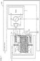
Fig.1 is a configuration diagram of a dielectric heating device of the invention according toEmbodiment 1. -
Fig.2 is a diagram showing another configuration diagram of a dielectric heating device of the invention according toEmbodiment 1. -
Fig.3 is a diagram showing another configuration diagram of a dielectric heating device of the invention according toEmbodiment 1. -
Fig.4 is a configuration diagram of a dielectric heating device of the invention according toEmbodiment 2. -
Fig.5 is a diagram showing another configuration diagram of a dielectric heating device of the invention according toEmbodiment 2. -
Fig.6 is a configuration diagram of a dielectric heating device of the invention according toEmbodiment 3. -
Fig.7 is a configuration diagram of a dielectric heating device of the invention according toEmbodiment 4. -
Fig.8 is another configuration diagram of a dielectric heating device of the invention according to each ofEmbodiment 1 toEmbodiment 4. -
Fig.9 is another configuration diagram of a dielectric heating device of the invention according to each ofEmbodiment 1 toEmbodiment 4. - Hereinafter, for illustrating the invention in more detail, embodiments for carrying out the invention will be described with reference to the accompanying drawings.
-
Fig.1 is a configuration diagram of adielectric heating device 100 of the invention according toEmbodiment 1. - The
dielectric heating device 100 is provided as an unbalanced circuit which includesdielectric heating electrodes 1, asignal source 2 and agrounded surface 3 that are each connected by means of unbalanced lines. - The
dielectric heating electrodes 1 includeelectrodes 10 and high-frequency passing heat-insulation elements 11 that cause only a high-frequency signal to pass therethrough and that inhibit heat transfer therethrough. Here, the high-frequency passing heat-insulation elements 11 each have two terminals of a terminal i and a terminal ii. The terminal i and the terminal ii have no metallically-continuous structure, and thus have a structure in which a conductor of the terminal i and a conductor of the terminal ii are not in contact with each other. Further, the terminal i and the terminal ii has a heat-insulation member having a high thermal resistance between the metals of the terminals, so that heat transfer therebetween is suppressed. On the other hand, using electric coupling between the metals, the terminal i and the terminal ii cause only a high-frequency signal to pass therebetween. Note that the two terminals are not metallically continuous and thus have a feature of not allowing a direct-current component to pass therebetween, and specific exemplary devices include a capacitor, a transformer, and a coupler. - Here, for simplification's sake, it is assumed that the coupling degree of electric coupling between the terminal i and the terminal ii is sufficiently high, so that the signal inputted through the terminal i is fully outputted from the terminal ii without being attenuated, and the signal inputted through the terminal ii also is fully outputted from the terminal i without being attenuated. It is further assumed that the thermal resistance between the terminal i and the terminal ii is very high, so that heat entering through the terminal i does not transfer to the terminal ii and heat entering through the terminal ii does not transfer to the terminal i.
- Furthermore, in the description of this embodiment, on the assumption that the
dielectric heating device 100 is a small-size device, a metal whose area is the largest in thedielectric heating device 100 and is sufficiently larger than areas of theelectrodes grounded surface 3. Accordingly, the heat capacity of thegrounded surface 3 is assumed to be large, as a relative value in comparison to the heat capacities of theelectrodes dielectric heating device 100 is small in size as a whole, the absolute value of the heat capacity of thegrounded surface 3 is assumed to be small. Thegrounded surface 3 may be set appropriately. - With reference to
Fig.1 , description will be made about a specific configuration example of thedielectric heating device 100. - The
dielectric heating device 100 shown inFig.1 includes twodielectric heating electrodes 1a, 1b, thesignal source 2 and thegrounded surface 3. With respect to the dielectric heating electrode 1a, theelectrode 10a and the terminal i of the high-frequency passing heat-insulation element (first element) 11a are connected to each other by means of metal wiring, and one side of thesignal source 2 and the terminal ii of the high-frequency passing heat-insulation element 11a are connected to each other by means of metal wiring. With respect to thedielectric heating electrode 1b, theelectrode 10b and the terminal i of the high-frequency passing heat-insulation element (second element) 11b are connected to each other by means of metal wiring, and the terminal ii of the high-frequency passing heat-insulation element 11b is connected to thegrounded surface 3 by means of metal wiring. The other side of thesignal source 2 is connected to thegrounded surface 3. - When the
signal source 2 is turned ON, a high-frequency signal is outputted from thesignal source 2. The outputted high-frequency signal is inputted to the terminal ii of the high-frequency passing heat-insulation element 11a. The high-frequency passing heat-insulation element 11a outputs, from the terminal i, the high-frequency signal inputted through the terminal ii, without attenuating that signal. The high-frequency signal outputted from the terminal i is sent to theelectrode 10a. The high-frequency passing heat-insulation element 11b outputs, from the terminal ii, the high-frequency signal inputted through the terminal i by way of theelectrode 10a and theelectrode 10b. - On the other hand, the voltage applied by the
electrode 10a heats the heating target X, so that the temperature of the heating target X under heating is elevated. When the temperature of the heating target X is elevated, heat generated in the heating target X transfers to theelectrodes electrodes electrodes insulation elements insulation element electrodes insulation elements dielectric heating device 100 to efficiently heat the heating target X. - Assuming that the high-frequency passing heat-
insulation element 11a is not provided in thedielectric heating device 100, heat having transferred from the heating target X to theelectrode 10a transfers through thesignal source 2 to thegrounded surface 3. Likewise, assuming that the high-frequency passing heat-insulation element 11b is not provided, heat having transferred from the heating target X to theelectrode 10b transfers to thegrounded surface 3, directly. Thegrounded surface 3 is a metal whose area is the largest in the heating target X and thedielectric heating device 100, and thus the heat capacity of thegrounded surface 3 is larger than the heat capacity of the heating target X, so that the heating efficiency is degraded because of heat transfer, namely, because heat in the heating target X transfers through theelectrode 10a or theelectrode 10b to thegrounded surface 3. In particular, the smaller the sizes of theelectrodes dielectric heating device 100. Further, although the groundedsurface 3 is the largest metal in thedielectric heating device 100, the heat capacity, as the absolute value, of the grounded surface is not large. Thus, in the case where the temperature of the heating target X reaches a high temperature of 100°C or more, the temperature of the groundedsurface 3 itself will also be elevated because of the heat transfer. When heat in the groundedsurface 3 transfers to thesignal source 2, the temperature of thedielectric heating device 100 as a whole is elevated, so that the lifetime of thedielectric heating device 100 is deteriorated. - In contrast, in the
dielectric heating device 100 according toEmbodiment 1, the high-frequency passing heat-insulation element 11a that causes only the high-frequency signal to pass therethrough and that inhibits heat transfer therethrough, is disposed serially to theelectrode 10a and thesignal source 2; and the high-frequency passing heat-insulation element 11b is disposed serially to theelectrode 10b and the groundedsurface 3. This makes it possible to suppress heat transfer to both thesignal source 2 and the groundedsurface 3 without interrupting transmission of the high-frequency wave, thereby being able to enhance the heating efficiency of the dielectric heating device for the heating target X. In particular, the high-frequency passing heat-insulation element 11a suppresses direct heat transfer to thesignal source 2 through theelectrode 10a, thereby preventing temperature elevation of thesignal source 2 and preventing heat transfer to the groundedsurface 3 through thesignal source 2. Further, the high-frequency passing heat-insulation element 11b suppresses heat transfer to the groundedsurface 3 through theelectrode 10b, thereby preventing heat transfer to the groundedsurface 3. Accordingly, the operation temperature of thesignal source 2 as a component circuit can be kept low and thus, the deterioration due to high temperature is suppressed, so that it is possible to prolong the lifetime of thedielectric heating device 100. - It is noted that, in
Fig.1 , a case where twodielectric heating electrodes 1a, 1b are provided is shown as an example; however, the number of the dielectric heating electrodes to be arranged may be set appropriately as long as the number is two or more. - In addition, with reference to
Fig.2 andFig.3 , description will be made about other configuration examples of thedielectric heating device 100. -
Fig.2 andFig.3 are diagrams each showing another configuration example of a dielectric heating device of the invention according toEmbodiment 1. - The high-frequency passing heat-
insulation elements dielectric heating device 100A shown inFig.2 each have a structure in which, between two metals, a dielectric material having a high thermal resistance and a high dielectric constant, thereby improving the heat-insulation capability and strengthening the coupling between the terminal i and the terminal ii, so that the high-frequency pass-attenuation characteristic is improved. - The high-frequency passing heat-
insulation element 11a shown inFig.2 includes a capacitor or coupler configured with anelement electrode 30a, anelement electrode 30b and adielectric material 32a. The high-frequency passing heat-insulation element 11b includes a capacitor or coupler configured with anelement electrode 31a, anelement electrode 31b and adielectric material 32b. In each of the high-frequency passing heat-insulation elements element electrodes element electrodes dielectric material 32a is sandwiched between theelement electrodes dielectric material 32b is sandwiched between theelement electrodes - The high-frequency passing heat-
insulation elements dielectric heating device 100B shown inFig.3 represent a case where anelement electrode 30a, anelement electrode 30b, andelement electrodes element electrode 30a and the projecting portions of theelement electrode 31a are placed so that they are engaged alternately, and the projecting portions of theelement electrode 30b and the projecting portions of theelement electrode 31b are placed so that they are engaged alternately. Since the high-frequency passing heat-insulation elements Fig.3 , it is possible to increase the electrode areas. Accordingly, electric or magnetic coupling between theelement electrode 30a and theelement electrodes 31a and between theelement electrode 30b and theelement electrode 31b is enhanced, so that it is possible to obtain small-size high-frequency passing heat-insulation elements 11. - In
Fig.2 andFig.3 , configurations of the high-frequency passing heat-insulation elements element electrodes - As described above, according to
Embodiment 1, it is configured to include: two ormore electrodes surface 3 connected to any oneelectrode 10b of the electrodes; thesignal source 2 that is connected to theelectrode 10a other than the electrode connected to the groundedsurface 3, and that outputs a high-frequency signal; the high-frequency passing heat-insulation element 11a that is interposed serially between thesignal source 2 and theelectrode 10a connected to thesignal source 2, and that causes the high-frequency signal outputted from thesignal source 2 to pass through theelement 11a, by using electric coupling or magnetic coupling between two terminals in theelement 11a, the terminals being not connected to each other by metal; and the high-frequency passing heat-insulation element 11b that is interposed serially between the groundedsurface 3 and theelectrode 2 connected to the groundedsurface 3, and that, by using electric coupling between two terminals i, ii in theelement 11b, outputs the high-frequency signal outputted from thesignal source 2, to the groundedsurface 3. Thus, it is possible to restrain heat from transferring from the heating object through the electrodes or the like to the component circuit and the grounded surface, thereby suppressing reduction of the heating efficiency. Further, since heat is restrained from transferring to the component circuit and the grounded surface, it is possible to prevent the component circuit and the signal source from reaching a high-temperature state, thereby suppressing deterioration of the component circuit and the signal source due to high temperature, so that prolongation of the lifetime is achieved. -
Fig.4 is a configuration diagram of adielectric heating device 100C of the invention according toEmbodiment 2. - The
dielectric heating device 100C ofEmbodiment 2 corresponds to thedielectric heating device 100 described inEmbodiment 1 when thesignal source 2 is configured with abattery 20, asignal generator 21 and anamplifier 22. - Note that, in the following, with respect to the parts same as or equivalent to the configuration elements of the
dielectric heating device 100 of the invention according toEmbodiment 1, the same reference numerals as the reference numerals used inEmbodiment 1 are given thereto, and description thereof will be omitted or simplified. - The
battery 20 has a plus terminal and a minus terminal and outputs a constant voltage across the plus terminal and the minus terminal. Because of being configured with thebattery 20, thedielectric heating device 100C is downsized and thus is portable. Thesignal generator 21 generates a high-frequency signal. Theamplifier 22 amplifies the high-frequency signal generated by thesignal generator 21 up to the desired power. Thesignal source 2 and theamplifier 22 are each connected by means of unbalanced lines, and theamplifier 22 is assumed to be an unbalanced circuit capable of outputting high power. - With respect to the
signal generator 21 and theamplifier 22, their respective plus terminals are connected to the plus terminal of thebattery 20 and their respective minus terminals are connected to the minus terminal of thebattery 20 and to the groundedsurface 3. The output of theamplifier 22 is connected to the terminal ii of the high-frequency passing heat-insulation element 11a. -
Fig.5 is a diagram showing another configuration diagram of a dielectric heating device according toEmbodiment 1. - A
dielectric heating device 100D shown inFig.5 represents a case where, in thedielectric heating device 100C of the invention according toEmbodiment 2 shown inFig.4 , thesignal source 2 is configured with abattery 20, asignal generator 21 and anamplifier 22. - Further, though not illustrated, in the
dielectric heating device 100B of the invention according toEmbodiment 1 shown inFig.3 , thesignal source 2 may be configured with abattery 20, asignal generator 21 and anamplifier 22. - According to the configurations shown in
Fig.4 andFig.5 , it is possible to downsize thedielectric heating device 100C up to a portable size. Further, as has been described inEmbodiment 1, although the groundedsurface 3 is the largest metal in thedielectric heating device 100, the heat capacity, as the absolute value, of the grounded surface is not large. Thus, in the case where the temperature of the heating target X reaches a high temperature of 100°C or more, the temperature of the groundedsurface 3 itself will also be elevated because of the heat transfer. When heat in the groundedsurface 3 transfers to thesignal source 2, the temperature of thedielectric heating device 100 as a whole is elevated, so that a possibility arises that the lifetime of thebattery 20 is deteriorated or thebattery 20 is deformed. According to the embodiment, it is possible to suppress heat transfer from the heating target X to thebattery 20 through theelectrode 10a and the plus terminal or minus terminal connected to theamplifier 22 or thesignal source 2; or heat transfer from the target X to thebattery 20 through theelectrode 10b and the groundedsurface 3. This restrains the operation temperature of thebattery 20 from being elevated, and thus deterioration of thebattery 20 due to high temperature is suppressed, so that it is possible to prolong the lifetime of thebattery 20. - As described above, according to
Embodiment 2, in the case where thesignal source 2 is configured with thebattery 20 for outputting a constant voltage, thesignal generator 21 for generating a high-frequency signal on the basis of the voltage outputted by thebattery 20, and theamplifier 22 for amplifying the high-frequency signal generated by thesignal generator 21, it is possible to restrain heat from transferring to the component circuit, that is, the battery, the signal generator and the amplifier. Accordingly, the operation temperatures of the battery, the signal generator and the amplifier can be kept low and thus, it is possible to prevent the battery, the signal generator and the amplifier from being deteriorated in performance due to high temperature or to prevent the component circuit and the battery from being deformed, thereby achieving prolongation of the lifetimes. -
Fig.6 is a configuration diagram of adielectric heating device 100D of the invention according toEmbodiment 3. - The
dielectric heating device 100D ofEmbodiment 3 has a structure in which the high-frequency passing heat-insulation element 11a and the high-frequency passing heat-insulation element 11b also served as electrodes for heating the heating target X. - Note that, in the following, with respect to the parts same as or equivalent to the configuration elements of the
dielectric heating device 100A of the invention according toEmbodiment 1, the same reference numerals as the reference numerals used inEmbodiment 1 are given thereto, and description thereof will be omitted or simplified. - An
electrode 10a and anelectrode 10b are electrodes for heating the heating target X. Each of theelectrode 10a and theelectrode 10b is configured to also serve, partly or wholly, as an electrode for a corresponding one of a high-frequency passing heat-insulation element 11c and a high-frequency passing heat-insulation element 11d.Fig.6 shows a case where each of theelectrode 10a and theelectrode 10b also serves partly as the electrode for the corresponding one of the high-frequency passing heat-insulation element 11a and the high-frequency passing heat-insulation element 11b. - In
Fig.6 , thedielectric material 32a (its surface where theelement electrode 30a shown inFig.2 is to be formed) is made contact with a part of theelectrode 10a, so that theelement electrode 30a is configured to serve also as theelectrode 10a. Further, on an opposite surface of thedielectric material 32a to the surface subjected to contact, theelement electrode 31a is provided, thereby forming the high-frequency passing heat-insulation element 11c. - Likewise, the
dielectric material 32b (its surface where theelement electrode 31b shown inFig.2 is to be formed) is made contact with a part of theelectrode 10b, so that theelement electrode 31b is configured to serve also as theelectrode 10b. Further, on an opposite surface of thedielectric material 32b to the surface subjected to contact, theelement electrode 30b is provided, thereby forming the high-frequency passing heat-insulation element 11d. - The
element electrode 31a is connected to thesignal source 2 by means of wiring. Theelement electrode 30b is connected to the groundedsurface 3 by means of wiring. - According to the configuration shown in
Fig.6 , the wiring between the high-frequency passing heat-insulation element 11c and theelectrode 10a and the wiring between the high-frequency passing heat-insulation element 11d and theelectrode 10b are no longer required, so that the areas of metal surfaces in contact with the heating target X are reduced. Accordingly, it is possible to suppressheat transfer 5 from the metal surfaces to a surroundingenvironment 4. The surroundingenvironment 4 means, for example, a surrounding structural object and atmosphere. Theheat transfer 5 is indicated inFig.6 by an arrow extending from theelectrode 10a to the surroundingenvironment 4 and by an arrow extending from theelectrode 10b to the surroundingenvironment 4. - Though not illustrated, in the
dielectric heating device 100B of the invention according toEmbodiment 1 shown inFig.3 , each of theelectrode 10a and theelectrode 10b may be configured to also serve, partly or wholly, as an electrode for a corresponding one of the high-frequency passing heat-insulation element 11a and the high-frequency passing heat-insulation element 11a. - As described above, according to
Embodiment 3, the high-frequency passing heat-insulation element 11c includes two or more element electrodes and at least one of the element electrodes serves also as theelectrode 10a; and the second element includes two or more element electrodes and at least one of the element electrodes serves also as theelectrode 10b. Thus, it is possible to eliminate the wiring between the high-frequency passing heat-insulation element 11c and theelectrode 10a and the wiring between the high-frequency passing heat-insulation element 11d and theelectrode 10b, thereby reducing narrowly the areas of the metals in contact with the heating target. Further, it is possible to reduce heat transferring from the metal surfaces to the surrounding environment, thereby achieving downsizing of the dielectric heating device. -
Fig.7 is a configuration diagram of adielectric heating device 100F according toEmbodiment 4. - The
dielectric heating device 100F ofEmbodiment 4 corresponds to thedielectric heating device 100E described inEmbodiment 3 when thesignal source 2 is configured with abattery 20, asignal generator 21 and anamplifier 22. - Note that, in the following, with respect to the parts same as or equivalent to the configuration elements of the
dielectric heating device 100C of the invention according toEmbodiment 2, the same reference numerals as the reference numerals used inEmbodiment 2 are given thereto, and description thereof will be omitted or simplified. Likewise, with respect to the parts same as or equivalent to the configuration elements of thedielectric heating device 100D of the invention according toEmbodiment 3, the same reference numerals as the reference numerals used inEmbodiment 3 are given thereto, and description thereof will be omitted or simplified. - Though not illustrated, in the
dielectric heating device 100B of the invention according toEmbodiment 1 shown inFig.3 , it is allowed that each of theelectrode 10a and theelectrode 10b is configured to also serve, partly or wholly, as the electrode for a corresponding one of the high-frequency passing heat-insulation element 11a and the high-frequency passing heat-insulation element 11a, and further thesignal source 2 is configured with abattery 20, asignal generator 21 and anamplifier 22. - According to the configuration shown in
Fig.7 , the wiring between the high-frequency passing heat-insulation element 11c and theelectrode 10a and the wiring between the high-frequency passing heat-insulation element 11d and theelectrode 10b are no longer required, so that the areas of metal surfaces in contact with the heating target X are reduced. Accordingly, it is possible to suppressheat transfer 5 from the metal surfaces to the surroundingenvironment 4. - Further, according to the configuration shown in
Fig.7 , it is possible to downsize thedielectric heating device 100F. Further, it is possible to suppress heat transfer from the heating target X to thebattery 20, thereby restraining the operation temperature of thebattery 20 from being elevated to suppress deterioration of thebattery 20 due to high temperature, so that it is possible to prolong the lifetime of thebattery 20. - As described above, according to
Embodiment 4, in the case where thesignal source 2 is configured with thebattery 20 for outputting a constant voltage, thesignal generator 21 for generating a high-frequency signal on the basis of the voltage outputted by thebattery 20, and theamplifier 22 for amplifying the high-frequency signal generated by thesignal generator 21, it is possible to restrain heat from transferring to the component circuit, that is, the battery, the signal generator and the amplifier. Accordingly, the operation temperatures of the battery, the signal generator and the amplifier can be kept low and thus, it is possible to restrain the battery, the signal generator and the amplifier from being deteriorated due to high temperature, thereby achieving prolongation of the lifetimes. - Further, according to
Embodiment 4, the high-frequency passing heat-insulation element 11c includes two or more element electrodes and at least one of the element electrodes serves also as theelectrode 10a on one side; and the second element is configured with two or more element electrodes and at least one of the element electrodes serves also as theelectrode 10b on another side. Thus, it is possible to eliminate the wiring between the high-frequency passing heat-insulation element 11c and theelectrode 10a and the wiring between the high-frequency passing heat-insulation element 11d and theelectrode 10b, thereby reducing narrowly the areas of the metals in contact with the heating target. Further, it is possible to reduce heat transferring from the metal surfaces to the surrounding environment, thereby achieving downsizing of the dielectric heating device. - The
dielectric heating devices Embodiment 1 toEmbodiment 4, are each configurable even when the number of the dielectric heating electrodes is three or more.
Fig.8 andFig.9 are each another configuration diagram of the dielectric heating device of the invention according to any one ofEmbodiment 1 toEmbodiment 4. - In
Fig.8 , adielectric heating device 100G obtained by adding adielectric heating electrode 1c to thedielectric heating device 100 of the invention according toEmbodiment 1 shown inFig.1 , is shown as an example. - In
Fig.9 , adielectric heating device 100H obtained by addingdielectric heating electrodes dielectric heating device 100 of the invention according toEmbodiment 1 shown inFig.1 , is shown as an example. - Other than the above, unlimited combination of the embodiments, modification of any configuration element in the embodiments and omission of any configuration element in the embodiments may be made in the present invention, without departing from the scope of the invention.
- It is particularly preferable that the dielectric heating device according to the invention is used in a portable small-size heating device.
- 1, 1a, 1b: dielectric heating electrode, 2: signal source, 3: grounded surface, 4: surrounding environment, 5: heat transfer, 10, 10a, 10b: electrode, 11, 11a, 11b, 11c, 11d: high-frequency passing heat-insulation element, 30a, 30b, 31a, 31b: element electrode, 20: battery, 21: signal generator, 22: amplifier, 32a, 32b: dielectric material, 100, 100A, 100B, 100C, 100D, 100E, 100F, 100G, 100H: dielectric heating device.
Claims (4)
- A dielectric heating device, comprising:two or more electrodes;a grounded surface connected to one of the electrodes;a signal source that is connected to one of the electrodes other than the electrode connected to the grounded surface, to output a high-frequency signal;a first element that is interposed serially between the signal source and the electrode connected to the signal source, to cause the high-frequency signal outputted from the signal source to pass through the first element, by using electric coupling or magnetic coupling between two terminals in the first element, the two terminals being not connected to each other by metal; anda second element that is interposed serially between the grounded surface and the electrode connected to the grounded surface, to output, by using electric coupling between two terminals in the second element, the high-frequency signal outputted from the signal source, to the grounded surface.
- The dielectric heating device according to claim 1, wherein the first element includes two or more element electrodes that are not connected to each other by metal in the first element, and at least one of the element electrodes serves also as the electrode connected to the signal source; and
wherein the second element includes two or more element electrodes, and at least one of the element electrodes serves also as the electrode connected to the grounded surface. - The dielectric heating device according to claim 1 or claim 2, wherein the signal source includes:a battery to output a constant voltage;a signal generator to generate the high-frequency signal on a basis of the voltage outputted by the battery; andan amplifier to amplify the high-frequency signal generated by the signal generator.
- Dielectric heating electrodes comprising:two or more electrodes;a first element that is interposed serially between a signal source to output a high-frequency signal and one of the electrodes connected to the signal source, to cause the high-frequency signal outputted from the signal source to pass through the first element, by using electric coupling or magnetic coupling between two terminals in the first element, the two terminals being not connected to each other by metal; anda second element that is interposed serially between a grounded surface and one of the electrodes connected to the grounded surface, to output, by using electric coupling between two terminals in the second element, the high-frequency signal outputted from the signal source, to the grounded surface.
Applications Claiming Priority (1)
| Application Number | Priority Date | Filing Date | Title |
|---|---|---|---|
| PCT/JP2018/018756 WO2019220534A1 (en) | 2018-05-15 | 2018-05-15 | Dielectric heating device and dielectric heating electrode |
Publications (3)
| Publication Number | Publication Date |
|---|---|
| EP3780908A1 true EP3780908A1 (en) | 2021-02-17 |
| EP3780908A4 EP3780908A4 (en) | 2021-04-21 |
| EP3780908B1 EP3780908B1 (en) | 2022-06-08 |
Family
ID=65270590
Family Applications (1)
| Application Number | Title | Priority Date | Filing Date |
|---|---|---|---|
| EP18919096.0A Active EP3780908B1 (en) | 2018-05-15 | 2018-05-15 | Dielectric heating device and dielectric heating electrode |
Country Status (5)
| Country | Link |
|---|---|
| US (1) | US11297695B2 (en) |
| EP (1) | EP3780908B1 (en) |
| JP (1) | JP6463570B1 (en) |
| CN (1) | CN112106442B (en) |
| WO (1) | WO2019220534A1 (en) |
Families Citing this family (9)
| Publication number | Priority date | Publication date | Assignee | Title |
|---|---|---|---|---|
| US12057561B1 (en) | 2019-07-12 | 2024-08-06 | Ampcera Inc. | Systems and methods for induction heating of electrolytes |
| US12272809B1 (en) | 2019-11-16 | 2025-04-08 | Ampcera Inc. | Battery cell, battery module, battery pack, electric vehicle, and method of heating |
| DE102020115923B4 (en) * | 2019-12-23 | 2022-10-13 | crop.zone GmbH | Device for applying contact resistance-reducing media and applying electricity to plants |
| US11936028B1 (en) | 2020-07-13 | 2024-03-19 | Ampcera Inc. | Systems and methods for heating electrochemical systems |
| CN116783994A (en) * | 2021-02-18 | 2023-09-19 | 松下知识产权经营株式会社 | High frequency heating device |
| WO2022224393A1 (en) * | 2021-04-22 | 2022-10-27 | 三菱電機株式会社 | Dielectric heating electrode and dielectric heating device |
| CN113712265B (en) * | 2021-10-08 | 2024-08-13 | 海南摩尔兄弟科技有限公司 | Aerosol product, electronic atomizer and atomizing system |
| TWI872501B (en) * | 2023-03-30 | 2025-02-11 | 明遠精密科技股份有限公司 | Composite-type rapid annealing device and method |
| SE547471C2 (en) * | 2024-07-12 | 2025-09-30 | RadAnt BioPhysics AB | A device for heating a sample |
Family Cites Families (21)
| Publication number | Priority date | Publication date | Assignee | Title |
|---|---|---|---|---|
| US2436732A (en) * | 1944-05-12 | 1948-02-24 | Carborundum Co | High-frequency electric field heating |
| US2521797A (en) * | 1945-08-02 | 1950-09-12 | Rca Corp | Electronic heating method and apparatus |
| US2508382A (en) * | 1946-10-10 | 1950-05-23 | Armstrong Cork Co | Method and apparatus for dielectric heating |
| US2727212A (en) * | 1950-10-27 | 1955-12-13 | Westinghouse Electric Corp | Constant load voltage circuit |
| BE510618A (en) * | 1951-04-14 | |||
| GB794443A (en) * | 1955-08-02 | 1958-05-07 | Radio Heaters Ltd | Improvements in or relating to high frequency heating equipment |
| US3518396A (en) * | 1968-05-27 | 1970-06-30 | Chemetron Corp | Dielectric heating apparatus |
| US5641423A (en) * | 1995-03-23 | 1997-06-24 | Stericycle, Inc. | Radio frequency heating apparatus for rendering medical materials |
| US6657173B2 (en) * | 1998-04-21 | 2003-12-02 | State Board Of Higher Education On Behalf Of Oregon State University | Variable frequency automated capacitive radio frequency (RF) dielectric heating system |
| US7883609B2 (en) * | 1998-06-15 | 2011-02-08 | The Trustees Of Dartmouth College | Ice modification removal and prevention |
| US6169278B1 (en) * | 1999-03-19 | 2001-01-02 | Rockwell Collins, Inc. | Dielectric heating using spread-spectrum energy |
| US6417499B2 (en) * | 2000-07-06 | 2002-07-09 | Heatwave Drying Systems Ltd. | Dielectric heating using inductive coupling |
| JP2002246164A (en) * | 2001-02-21 | 2002-08-30 | Matsushita Electric Ind Co Ltd | High frequency thawing equipment |
| WO2002090081A1 (en) | 2001-05-09 | 2002-11-14 | Nissei Kabushiki Kaisha | Method of manufacturing hot formed object, and device and method for continuous high-frequency heating. |
| JP2002334775A (en) * | 2001-05-09 | 2002-11-22 | Nissei Co Ltd | Continuous high frequency heating device and continuous high frequency heating method |
| JP2004349116A (en) * | 2003-05-22 | 2004-12-09 | Mitsubishi Electric Corp | Dielectric heating device |
| US7091460B2 (en) * | 2004-03-15 | 2006-08-15 | Dwight Eric Kinzer | In situ processing of hydrocarbon-bearing formations with variable frequency automated capacitive radio frequency dielectric heating |
| JP2011061753A (en) | 2009-10-08 | 2011-03-24 | Mitsubishi Electric Corp | Digital broadcast receiving apparatus |
| JP5768972B2 (en) | 2011-09-30 | 2015-08-26 | 東洋製罐株式会社 | High frequency dielectric heating device |
| GB2512819B (en) * | 2013-03-18 | 2021-07-14 | Wayv Tech Limited | Microwave heating apparatus |
| EP3322258A4 (en) * | 2015-07-03 | 2019-03-27 | Toyo Seikan Group Holdings, Ltd. | HIGH FREQUENCY DIELECTRIC HEATING DEVICE |
-
2018
- 2018-05-15 JP JP2018553251A patent/JP6463570B1/en active Active
- 2018-05-15 CN CN201880093312.8A patent/CN112106442B/en active Active
- 2018-05-15 EP EP18919096.0A patent/EP3780908B1/en active Active
- 2018-05-15 WO PCT/JP2018/018756 patent/WO2019220534A1/en not_active Ceased
-
2020
- 2020-09-30 US US17/038,510 patent/US11297695B2/en active Active
Also Published As
| Publication number | Publication date |
|---|---|
| JP6463570B1 (en) | 2019-02-06 |
| EP3780908B1 (en) | 2022-06-08 |
| CN112106442B (en) | 2022-08-19 |
| CN112106442A (en) | 2020-12-18 |
| WO2019220534A1 (en) | 2019-11-21 |
| US11297695B2 (en) | 2022-04-05 |
| EP3780908A4 (en) | 2021-04-21 |
| US20210014942A1 (en) | 2021-01-14 |
| JPWO2019220534A1 (en) | 2020-05-28 |
Similar Documents
| Publication | Publication Date | Title |
|---|---|---|
| US11297695B2 (en) | Dielectric heating device and dielectric heating electrodes | |
| JP7146983B2 (en) | Solid-state microwave oscillators and power amplifiers | |
| US8193857B1 (en) | Wideband doherty amplifier circuit | |
| Hooda et al. | A Generalized Measure of ‘Useful R-norm Information | |
| Sánchez-Pérez et al. | Design and large-signal characterization of high-power varactor-based impedance tuners | |
| Chandravanshi et al. | Design of efficient rectifier using IDC and harmonic rejection filter in GSM/CDMA band for RF energy harvesting | |
| CN104242840A (en) | Amplification apparatus | |
| CN104081662B (en) | Method and device for protecting a high-frequency power amplifier against a termination fault | |
| JPWO2021205801A5 (en) | ||
| Kilic et al. | Highly efficient dual‐band GaN power amplifier utilising pin diode‐based tunable harmonic load matching | |
| CN108092677B (en) | Transmitting assembly | |
| Suzuki et al. | Multiplex transmission system for gate drive signals of inverter circuit using surface acoustic wave filters | |
| US9461353B2 (en) | Power combiner and power divider | |
| Tanaka et al. | A 2‐GHz GaN HEMT Power Amplifier Harmonically Tuned Using a Compact One‐Port CRLH Transmission Line | |
| Noh et al. | Ku‐band GaN HPA MMIC with high‐power and high‐PAE performances | |
| Nakade et al. | Development of 150W S-band GaN solid state power amplifier for satellite use | |
| Van Heijningen et al. | L-band AlGaN/GaN power amplifier with protection against load mismatch | |
| JP2022527392A (en) | Trapezoidal power barrier between dangerous and normal locations | |
| Kubo et al. | Design of surface acoustic wave filters for the multiplex transmission system of multilevel inverter circuits | |
| Giofre et al. | A high-power solid state amplifier for Galileo satellite system exploiting European GaN technology | |
| Kumar et al. | High performance S-band GaN T/R module using hybrid microwave integrated circuit | |
| Kido et al. | 100W C-band GaN solid state power amplifier with 50% PAE for satellite use | |
| JP2018133698A (en) | Power amplifier | |
| Hirano et al. | 70W C-band GaN solid state power amplifier for satellite use | |
| Giofré et al. | A GaN high power and efficient amplifier for L-Band Galileo system |
Legal Events
| Date | Code | Title | Description |
|---|---|---|---|
| STAA | Information on the status of an ep patent application or granted ep patent |
Free format text: STATUS: THE INTERNATIONAL PUBLICATION HAS BEEN MADE |
|
| PUAI | Public reference made under article 153(3) epc to a published international application that has entered the european phase |
Free format text: ORIGINAL CODE: 0009012 |
|
| STAA | Information on the status of an ep patent application or granted ep patent |
Free format text: STATUS: REQUEST FOR EXAMINATION WAS MADE |
|
| 17P | Request for examination filed |
Effective date: 20201102 |
|
| AK | Designated contracting states |
Kind code of ref document: A1 Designated state(s): AL AT BE BG CH CY CZ DE DK EE ES FI FR GB GR HR HU IE IS IT LI LT LU LV MC MK MT NL NO PL PT RO RS SE SI SK SM TR |
|
| AX | Request for extension of the european patent |
Extension state: BA ME |
|
| REG | Reference to a national code |
Ref country code: DE Ref legal event code: R079 Ref document number: 602018036653 Country of ref document: DE Free format text: PREVIOUS MAIN CLASS: H05B0006480000 Ipc: H05B0006620000 |
|
| A4 | Supplementary search report drawn up and despatched |
Effective date: 20210319 |
|
| RIC1 | Information provided on ipc code assigned before grant |
Ipc: H05B 6/62 20060101AFI20210315BHEP |
|
| DAV | Request for validation of the european patent (deleted) | ||
| DAX | Request for extension of the european patent (deleted) | ||
| STAA | Information on the status of an ep patent application or granted ep patent |
Free format text: STATUS: EXAMINATION IS IN PROGRESS |
|
| 17Q | First examination report despatched |
Effective date: 20210915 |
|
| GRAP | Despatch of communication of intention to grant a patent |
Free format text: ORIGINAL CODE: EPIDOSNIGR1 |
|
| STAA | Information on the status of an ep patent application or granted ep patent |
Free format text: STATUS: GRANT OF PATENT IS INTENDED |
|
| INTG | Intention to grant announced |
Effective date: 20220208 |
|
| GRAS | Grant fee paid |
Free format text: ORIGINAL CODE: EPIDOSNIGR3 |
|
| GRAA | (expected) grant |
Free format text: ORIGINAL CODE: 0009210 |
|
| STAA | Information on the status of an ep patent application or granted ep patent |
Free format text: STATUS: THE PATENT HAS BEEN GRANTED |
|
| AK | Designated contracting states |
Kind code of ref document: B1 Designated state(s): AL AT BE BG CH CY CZ DE DK EE ES FI FR GB GR HR HU IE IS IT LI LT LU LV MC MK MT NL NO PL PT RO RS SE SI SK SM TR |
|
| REG | Reference to a national code |
Ref country code: AT Ref legal event code: REF Ref document number: 1497798 Country of ref document: AT Kind code of ref document: T Effective date: 20220615 Ref country code: CH Ref legal event code: EP |
|
| REG | Reference to a national code |
Ref country code: DE Ref legal event code: R096 Ref document number: 602018036653 Country of ref document: DE |
|
| REG | Reference to a national code |
Ref country code: IE Ref legal event code: FG4D |
|
| REG | Reference to a national code |
Ref country code: LT Ref legal event code: MG9D |
|
| REG | Reference to a national code |
Ref country code: NL Ref legal event code: MP Effective date: 20220608 |
|
| PG25 | Lapsed in a contracting state [announced via postgrant information from national office to epo] |
Ref country code: SE Free format text: LAPSE BECAUSE OF FAILURE TO SUBMIT A TRANSLATION OF THE DESCRIPTION OR TO PAY THE FEE WITHIN THE PRESCRIBED TIME-LIMIT Effective date: 20220608 Ref country code: NO Free format text: LAPSE BECAUSE OF FAILURE TO SUBMIT A TRANSLATION OF THE DESCRIPTION OR TO PAY THE FEE WITHIN THE PRESCRIBED TIME-LIMIT Effective date: 20220908 Ref country code: LT Free format text: LAPSE BECAUSE OF FAILURE TO SUBMIT A TRANSLATION OF THE DESCRIPTION OR TO PAY THE FEE WITHIN THE PRESCRIBED TIME-LIMIT Effective date: 20220608 Ref country code: HR Free format text: LAPSE BECAUSE OF FAILURE TO SUBMIT A TRANSLATION OF THE DESCRIPTION OR TO PAY THE FEE WITHIN THE PRESCRIBED TIME-LIMIT Effective date: 20220608 Ref country code: GR Free format text: LAPSE BECAUSE OF FAILURE TO SUBMIT A TRANSLATION OF THE DESCRIPTION OR TO PAY THE FEE WITHIN THE PRESCRIBED TIME-LIMIT Effective date: 20220909 Ref country code: FI Free format text: LAPSE BECAUSE OF FAILURE TO SUBMIT A TRANSLATION OF THE DESCRIPTION OR TO PAY THE FEE WITHIN THE PRESCRIBED TIME-LIMIT Effective date: 20220608 Ref country code: BG Free format text: LAPSE BECAUSE OF FAILURE TO SUBMIT A TRANSLATION OF THE DESCRIPTION OR TO PAY THE FEE WITHIN THE PRESCRIBED TIME-LIMIT Effective date: 20220908 |
|
| REG | Reference to a national code |
Ref country code: AT Ref legal event code: MK05 Ref document number: 1497798 Country of ref document: AT Kind code of ref document: T Effective date: 20220608 |
|
| PG25 | Lapsed in a contracting state [announced via postgrant information from national office to epo] |
Ref country code: RS Free format text: LAPSE BECAUSE OF FAILURE TO SUBMIT A TRANSLATION OF THE DESCRIPTION OR TO PAY THE FEE WITHIN THE PRESCRIBED TIME-LIMIT Effective date: 20220608 Ref country code: LV Free format text: LAPSE BECAUSE OF FAILURE TO SUBMIT A TRANSLATION OF THE DESCRIPTION OR TO PAY THE FEE WITHIN THE PRESCRIBED TIME-LIMIT Effective date: 20220608 |
|
| PG25 | Lapsed in a contracting state [announced via postgrant information from national office to epo] |
Ref country code: NL Free format text: LAPSE BECAUSE OF FAILURE TO SUBMIT A TRANSLATION OF THE DESCRIPTION OR TO PAY THE FEE WITHIN THE PRESCRIBED TIME-LIMIT Effective date: 20220608 |
|
| PG25 | Lapsed in a contracting state [announced via postgrant information from national office to epo] |
Ref country code: SM Free format text: LAPSE BECAUSE OF FAILURE TO SUBMIT A TRANSLATION OF THE DESCRIPTION OR TO PAY THE FEE WITHIN THE PRESCRIBED TIME-LIMIT Effective date: 20220608 Ref country code: SK Free format text: LAPSE BECAUSE OF FAILURE TO SUBMIT A TRANSLATION OF THE DESCRIPTION OR TO PAY THE FEE WITHIN THE PRESCRIBED TIME-LIMIT Effective date: 20220608 Ref country code: RO Free format text: LAPSE BECAUSE OF FAILURE TO SUBMIT A TRANSLATION OF THE DESCRIPTION OR TO PAY THE FEE WITHIN THE PRESCRIBED TIME-LIMIT Effective date: 20220608 Ref country code: PT Free format text: LAPSE BECAUSE OF FAILURE TO SUBMIT A TRANSLATION OF THE DESCRIPTION OR TO PAY THE FEE WITHIN THE PRESCRIBED TIME-LIMIT Effective date: 20221010 Ref country code: ES Free format text: LAPSE BECAUSE OF FAILURE TO SUBMIT A TRANSLATION OF THE DESCRIPTION OR TO PAY THE FEE WITHIN THE PRESCRIBED TIME-LIMIT Effective date: 20220608 Ref country code: EE Free format text: LAPSE BECAUSE OF FAILURE TO SUBMIT A TRANSLATION OF THE DESCRIPTION OR TO PAY THE FEE WITHIN THE PRESCRIBED TIME-LIMIT Effective date: 20220608 Ref country code: CZ Free format text: LAPSE BECAUSE OF FAILURE TO SUBMIT A TRANSLATION OF THE DESCRIPTION OR TO PAY THE FEE WITHIN THE PRESCRIBED TIME-LIMIT Effective date: 20220608 Ref country code: AT Free format text: LAPSE BECAUSE OF FAILURE TO SUBMIT A TRANSLATION OF THE DESCRIPTION OR TO PAY THE FEE WITHIN THE PRESCRIBED TIME-LIMIT Effective date: 20220608 |
|
| PG25 | Lapsed in a contracting state [announced via postgrant information from national office to epo] |
Ref country code: PL Free format text: LAPSE BECAUSE OF FAILURE TO SUBMIT A TRANSLATION OF THE DESCRIPTION OR TO PAY THE FEE WITHIN THE PRESCRIBED TIME-LIMIT Effective date: 20220608 Ref country code: IS Free format text: LAPSE BECAUSE OF FAILURE TO SUBMIT A TRANSLATION OF THE DESCRIPTION OR TO PAY THE FEE WITHIN THE PRESCRIBED TIME-LIMIT Effective date: 20221008 |
|
| REG | Reference to a national code |
Ref country code: DE Ref legal event code: R097 Ref document number: 602018036653 Country of ref document: DE |
|
| PG25 | Lapsed in a contracting state [announced via postgrant information from national office to epo] |
Ref country code: AL Free format text: LAPSE BECAUSE OF FAILURE TO SUBMIT A TRANSLATION OF THE DESCRIPTION OR TO PAY THE FEE WITHIN THE PRESCRIBED TIME-LIMIT Effective date: 20220608 |
|
| PLBE | No opposition filed within time limit |
Free format text: ORIGINAL CODE: 0009261 |
|
| STAA | Information on the status of an ep patent application or granted ep patent |
Free format text: STATUS: NO OPPOSITION FILED WITHIN TIME LIMIT |
|
| PG25 | Lapsed in a contracting state [announced via postgrant information from national office to epo] |
Ref country code: DK Free format text: LAPSE BECAUSE OF FAILURE TO SUBMIT A TRANSLATION OF THE DESCRIPTION OR TO PAY THE FEE WITHIN THE PRESCRIBED TIME-LIMIT Effective date: 20220608 |
|
| 26N | No opposition filed |
Effective date: 20230310 |
|
| PG25 | Lapsed in a contracting state [announced via postgrant information from national office to epo] |
Ref country code: SI Free format text: LAPSE BECAUSE OF FAILURE TO SUBMIT A TRANSLATION OF THE DESCRIPTION OR TO PAY THE FEE WITHIN THE PRESCRIBED TIME-LIMIT Effective date: 20220608 |
|
| REG | Reference to a national code |
Ref country code: DE Ref legal event code: R119 Ref document number: 602018036653 Country of ref document: DE |
|
| PG25 | Lapsed in a contracting state [announced via postgrant information from national office to epo] |
Ref country code: MC Free format text: LAPSE BECAUSE OF FAILURE TO SUBMIT A TRANSLATION OF THE DESCRIPTION OR TO PAY THE FEE WITHIN THE PRESCRIBED TIME-LIMIT Effective date: 20220608 |
|
| REG | Reference to a national code |
Ref country code: BE Ref legal event code: MM Effective date: 20230531 |
|
| PG25 | Lapsed in a contracting state [announced via postgrant information from national office to epo] |
Ref country code: MC Free format text: LAPSE BECAUSE OF FAILURE TO SUBMIT A TRANSLATION OF THE DESCRIPTION OR TO PAY THE FEE WITHIN THE PRESCRIBED TIME-LIMIT Effective date: 20220608 Ref country code: LU Free format text: LAPSE BECAUSE OF NON-PAYMENT OF DUE FEES Effective date: 20230515 Ref country code: IT Free format text: LAPSE BECAUSE OF FAILURE TO SUBMIT A TRANSLATION OF THE DESCRIPTION OR TO PAY THE FEE WITHIN THE PRESCRIBED TIME-LIMIT Effective date: 20220608 |
|
| REG | Reference to a national code |
Ref country code: IE Ref legal event code: MM4A |
|
| PG25 | Lapsed in a contracting state [announced via postgrant information from national office to epo] |
Ref country code: IE Free format text: LAPSE BECAUSE OF NON-PAYMENT OF DUE FEES Effective date: 20230515 |
|
| PG25 | Lapsed in a contracting state [announced via postgrant information from national office to epo] |
Ref country code: IE Free format text: LAPSE BECAUSE OF NON-PAYMENT OF DUE FEES Effective date: 20230515 Ref country code: DE Free format text: LAPSE BECAUSE OF NON-PAYMENT OF DUE FEES Effective date: 20231201 |
|
| PG25 | Lapsed in a contracting state [announced via postgrant information from national office to epo] |
Ref country code: FR Free format text: LAPSE BECAUSE OF NON-PAYMENT OF DUE FEES Effective date: 20230531 Ref country code: BE Free format text: LAPSE BECAUSE OF NON-PAYMENT OF DUE FEES Effective date: 20230531 |
|
| REG | Reference to a national code |
Ref country code: GB Ref legal event code: 746 Effective date: 20240531 |
|
| PG25 | Lapsed in a contracting state [announced via postgrant information from national office to epo] |
Ref country code: BG Free format text: LAPSE BECAUSE OF FAILURE TO SUBMIT A TRANSLATION OF THE DESCRIPTION OR TO PAY THE FEE WITHIN THE PRESCRIBED TIME-LIMIT Effective date: 20220608 |
|
| PG25 | Lapsed in a contracting state [announced via postgrant information from national office to epo] |
Ref country code: BG Free format text: LAPSE BECAUSE OF FAILURE TO SUBMIT A TRANSLATION OF THE DESCRIPTION OR TO PAY THE FEE WITHIN THE PRESCRIBED TIME-LIMIT Effective date: 20220608 |
|
| PGFP | Annual fee paid to national office [announced via postgrant information from national office to epo] |
Ref country code: GB Payment date: 20250327 Year of fee payment: 8 |
|
| PGFP | Annual fee paid to national office [announced via postgrant information from national office to epo] |
Ref country code: CH Payment date: 20250601 Year of fee payment: 8 |
|
| PG25 | Lapsed in a contracting state [announced via postgrant information from national office to epo] |
Ref country code: CY Free format text: LAPSE BECAUSE OF FAILURE TO SUBMIT A TRANSLATION OF THE DESCRIPTION OR TO PAY THE FEE WITHIN THE PRESCRIBED TIME-LIMIT; INVALID AB INITIO Effective date: 20180515 |
|
| PG25 | Lapsed in a contracting state [announced via postgrant information from national office to epo] |
Ref country code: HU Free format text: LAPSE BECAUSE OF FAILURE TO SUBMIT A TRANSLATION OF THE DESCRIPTION OR TO PAY THE FEE WITHIN THE PRESCRIBED TIME-LIMIT; INVALID AB INITIO Effective date: 20180515 |
|
| PG25 | Lapsed in a contracting state [announced via postgrant information from national office to epo] |
Ref country code: TR Free format text: LAPSE BECAUSE OF FAILURE TO SUBMIT A TRANSLATION OF THE DESCRIPTION OR TO PAY THE FEE WITHIN THE PRESCRIBED TIME-LIMIT Effective date: 20220608 |