EP3780774A1 - Method and device for determining power control offset for pucch - Google Patents
Method and device for determining power control offset for pucch Download PDFInfo
- Publication number
- EP3780774A1 EP3780774A1 EP18912041.3A EP18912041A EP3780774A1 EP 3780774 A1 EP3780774 A1 EP 3780774A1 EP 18912041 A EP18912041 A EP 18912041A EP 3780774 A1 EP3780774 A1 EP 3780774A1
- Authority
- EP
- European Patent Office
- Prior art keywords
- pucch
- uci
- determining
- format
- symb
- Prior art date
- Legal status (The legal status is an assumption and is not a legal conclusion. Google has not performed a legal analysis and makes no representation as to the accuracy of the status listed.)
- Granted
Links
Images

Classifications
-
- H—ELECTRICITY
- H04—ELECTRIC COMMUNICATION TECHNIQUE
- H04W—WIRELESS COMMUNICATION NETWORKS
- H04W52/00—Power management, e.g. Transmission Power Control [TPC] or power classes
- H04W52/04—Transmission power control [TPC]
- H04W52/30—Transmission power control [TPC] using constraints in the total amount of available transmission power
- H04W52/36—Transmission power control [TPC] using constraints in the total amount of available transmission power with a discrete range or set of values, e.g. step size, ramping or offsets
- H04W52/362—Aspects of the step size
-
- H—ELECTRICITY
- H04—ELECTRIC COMMUNICATION TECHNIQUE
- H04W—WIRELESS COMMUNICATION NETWORKS
- H04W52/00—Power management, e.g. Transmission Power Control [TPC] or power classes
- H04W52/04—Transmission power control [TPC]
- H04W52/06—TPC algorithms
-
- H—ELECTRICITY
- H04—ELECTRIC COMMUNICATION TECHNIQUE
- H04L—TRANSMISSION OF DIGITAL INFORMATION, e.g. TELEGRAPHIC COMMUNICATION
- H04L5/00—Arrangements affording multiple use of the transmission path
- H04L5/02—Channels characterised by the type of signal
- H04L5/06—Channels characterised by the type of signal the signals being represented by different frequencies
- H04L5/10—Channels characterised by the type of signal the signals being represented by different frequencies with dynamo-electric generation of carriers; with mechanical filters or demodulators
-
- H—ELECTRICITY
- H04—ELECTRIC COMMUNICATION TECHNIQUE
- H04W—WIRELESS COMMUNICATION NETWORKS
- H04W52/00—Power management, e.g. Transmission Power Control [TPC] or power classes
- H04W52/04—Transmission power control [TPC]
- H04W52/06—TPC algorithms
- H04W52/14—Separate analysis of uplink or downlink
- H04W52/146—Uplink power control
-
- H—ELECTRICITY
- H04—ELECTRIC COMMUNICATION TECHNIQUE
- H04W—WIRELESS COMMUNICATION NETWORKS
- H04W52/00—Power management, e.g. Transmission Power Control [TPC] or power classes
- H04W52/04—Transmission power control [TPC]
- H04W52/18—TPC being performed according to specific parameters
-
- H—ELECTRICITY
- H04—ELECTRIC COMMUNICATION TECHNIQUE
- H04W—WIRELESS COMMUNICATION NETWORKS
- H04W52/00—Power management, e.g. Transmission Power Control [TPC] or power classes
- H04W52/04—Transmission power control [TPC]
- H04W52/30—Transmission power control [TPC] using constraints in the total amount of available transmission power
- H04W52/32—TPC of broadcast or control channels
- H04W52/325—Power control of control or pilot channels
-
- H—ELECTRICITY
- H04—ELECTRIC COMMUNICATION TECHNIQUE
- H04W—WIRELESS COMMUNICATION NETWORKS
- H04W52/00—Power management, e.g. Transmission Power Control [TPC] or power classes
- H04W52/04—Transmission power control [TPC]
- H04W52/30—Transmission power control [TPC] using constraints in the total amount of available transmission power
- H04W52/36—Transmission power control [TPC] using constraints in the total amount of available transmission power with a discrete range or set of values, e.g. step size, ramping or offsets
-
- H—ELECTRICITY
- H04—ELECTRIC COMMUNICATION TECHNIQUE
- H04W—WIRELESS COMMUNICATION NETWORKS
- H04W72/00—Local resource management
- H04W72/20—Control channels or signalling for resource management
- H04W72/21—Control channels or signalling for resource management in the uplink direction of a wireless link, i.e. towards the network
-
- H—ELECTRICITY
- H04—ELECTRIC COMMUNICATION TECHNIQUE
- H04B—TRANSMISSION
- H04B1/00—Details of transmission systems, not covered by a single one of groups H04B3/00 - H04B13/00; Details of transmission systems not characterised by the medium used for transmission
- H04B1/69—Spread spectrum techniques
- H04B1/713—Spread spectrum techniques using frequency hopping
-
- H—ELECTRICITY
- H04—ELECTRIC COMMUNICATION TECHNIQUE
- H04L—TRANSMISSION OF DIGITAL INFORMATION, e.g. TELEGRAPHIC COMMUNICATION
- H04L5/00—Arrangements affording multiple use of the transmission path
- H04L5/003—Arrangements for allocating sub-channels of the transmission path
- H04L5/0048—Allocation of pilot signals, i.e. of signals known to the receiver
- H04L5/0051—Allocation of pilot signals, i.e. of signals known to the receiver of dedicated pilots, i.e. pilots destined for a single user or terminal
-
- H—ELECTRICITY
- H04—ELECTRIC COMMUNICATION TECHNIQUE
- H04L—TRANSMISSION OF DIGITAL INFORMATION, e.g. TELEGRAPHIC COMMUNICATION
- H04L5/00—Arrangements affording multiple use of the transmission path
- H04L5/003—Arrangements for allocating sub-channels of the transmission path
- H04L5/0053—Allocation of signalling, i.e. of overhead other than pilot signals
-
- H—ELECTRICITY
- H04—ELECTRIC COMMUNICATION TECHNIQUE
- H04L—TRANSMISSION OF DIGITAL INFORMATION, e.g. TELEGRAPHIC COMMUNICATION
- H04L5/00—Arrangements affording multiple use of the transmission path
- H04L5/0091—Signalling for the administration of the divided path, e.g. signalling of configuration information
Definitions
- the present application relates to the field of communication technologies, and particularly to a method and device for determining a Physical Uplink Control Channel (PUCCH) power control offset.
- PUCCH Physical Uplink Control Channel
- 5G NR 5 Generation New RAT
- P PUCCH , c i min P CMAX , c i , P 0 _ PUCCH , c b + PL c k + ⁇ F _ PUCCH , c F + ⁇ PUCCH _ TF , c i + g c i l dBm
- the PUCCH uses a new Polar coding scheme, of which the performance is improved significantly compared to the Tail Biting CC (TBCC) coding scheme of the Long Term Evolution (LTE) system.
- TBCC Tail Biting CC
- LTE Long Term Evolution
- the Polar coding scheme requires the less power, thereby reducing the power consumption of the terminal.
- the NR supports new PUCCH formats, such as PUCCH format 0, PUCCH format 1, PUCCH format 2, PUCCH format 3, and PUCCH format 4.
- the existing method for determining the power control offset ⁇ PUCCH_TF,c (i) for the PUCCH cannot adapt to the new power control method and coding scheme adopted in the NR.
- Embodiments of the present application provide a method and device for determining a PUCCH power control offset, so as to provide a new solution for determining the PUCCH power control offset, to solve the technical problem that the existing method for determining the PUCCH power control offset cannot adapt to the new wireless communication system.
- a method for determining a PUCCH power control offset including:
- the determining the quantity N RE of REs bearing the UCI in the PUCCH includes:
- g(O UCI / N RE ) is a linear fitting function with Ouci and N RE being variables.
- g(O UCI / N RE ) is a*(O UCI /N RE ) + b, wherein a and b are tuning coefficients, 1.5 ⁇ a ⁇ 2.5, and -1 ⁇ b ⁇ 1.
- a terminal which includes:
- the processor determines the quantity N RE of REs bearing the UCI in the PUCCH by:
- g(O UCI / N RE ) is a linear fitting function with Ouci and N RE being variables.
- g(O UCI / N RE ) is a*(O UCI /N RE ) + b, wherein a and b are tuning coefficients, 1.5 ⁇ a ⁇ 2.5, and -1 ⁇ b ⁇ 1.
- a terminal which includes:
- the first determining module is configured to:
- g(O UCI / N RE ) is a linear fitting function with Ouci and N RE being variables.
- g(O UCI / N RE ) is a*(O UCI /N RE ) + b, wherein a and b are tuning coefficients, 1.5 ⁇ a ⁇ 2.5, and -1 ⁇ b ⁇ 1.
- a and b include a plurality of preset values respectively, and the second determining module is configured to: determine values of a and b corresponding to a PUCCH format used for transmitting the first UCI, the Ouci of the first UCI, and a frequency hopping situation.
- a computer readable storage medium is provided.
- the computer readable storage medium stores computer instructions, which cause a computer device to perform the method as described in the first aspect when running on the computer device.
- g(O UCI / N RE ) is a function with Ouci and N RE being variables.
- the base station adjusts the power of the user terminal by way of open-loop and closed-loop power control, and the base station feeds back the power control information to the UE according to the UE uplink measurement result and adjusts the uplink transmit power obtained by the UE through the open-loop power control, and thus can control the transmit power of the UE more accurately.
- the LTE uses ⁇ TF,c (i) as a parameter in the calculation of the Physical Uplink Shared Channel (PUSCH) power
- BPRE O CQI / N RE
- O CQI is the bit length of the Cyclic Redundancy Checksum (CRC)contained in the Channel Quality Indicator (CQI)/Pre-coding Matrix Indicator (PMI)
- the PUCCH formats used in the LTE are different from the PUCCH formats in the NR.
- the NR supports 5 new PUCCH formats: the PUCCH format 0 is a short PUCCH format of 2 bits or less; the PUCCH format 1 is a long PUCCH format of 2 bits or less; the PUCCH format 2 is a short PUCCH format of 2 bits or more; the PUCCH format 3 is a short PUCCH format of 2 bits or more and does not support multi-user multiplexing; and the PUCCH format 4 is a short PUCCH format of 2 bits or more and supports multi-user multiplexing.
- the TBCC coding is used in the LTE, and the coding combination scheme of CA-Polar and PC CA-Polar is used in the NR.
- the performance of the NR scheme is much better than that of the LTE. Since the PUCCH formats, bit range, coding scheme, etc. used in the NR are all different, the reuse of ⁇ PUCCH_TF,c (i) in the LTE may reduce the transmission performance of the PUCCH in the NR.
- the offset used in the power control calculation performed for the NR PUCCH format 2/3/4 also needs to be different from that of LTE, to adapt to the new power control method and coding scheme in the NR.
- the idea of the embodiments of the present application is to consider the calculation method of Signal to Noise Ratio (SNR) in the information theory.
- SNR Signal to Noise Ratio
- the embodiment of the present application provides a method for determining a PUCCH power control offset, where the method can be applied to a terminal, e.g., a mobile phone, a tablet computer, a personal computer, a notebook computer, a wearable electronic device, and other devices with communication functions.
- a terminal e.g., a mobile phone, a tablet computer, a personal computer, a notebook computer, a wearable electronic device, and other devices with communication functions.
- Step 101 determining a quantity Ouci of bits of the first UCI required to be transmitted on a PUCCH, and determine a quantity N RE of REs bearing the first UCI in the PUCCH.
- Ouci may mean the number of bits of the CRC contained in the UCI.
- the formula of calculating ⁇ PUCCH_TF,c (i) in some embodiments of the present application may be set to be used only in the case of Ouci > 17 bits.
- the quantity N RE of REs bearing the first UCI in the PUCCH is determined in different ways.
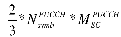
- N symb PUCCH is a quantity of PUCCH symbols occupied by the UCI defined in the PUCCH format 4
- N DMRS ⁇ symb PUCCH is a quantity of PUCCH symbols occupied by a DMRS defined in the PUCCH format 4
- M SC PUCCH is the PUCCH bandwidth occupied by the UCI defined in the PUCCH format 4.
- ⁇ PUCCH_TF,c (i) is calculated by using different parameters for the PUCCH format 2 and PUCCH format 3/4.
- g(O UCI / N RE ) in the formula ⁇ PUCCH_TF,c ( i ) 10 log 10 (2 g ( O UCI / N RE ) -1) is a linear fitting function with O UCI and N RE being variables.
- a and b are tuning coefficients which are preset values, where the value range of a may be [1.5, 2.5], and the value range of b may be [-1, 1], that is, 1.5 ⁇ a ⁇ 2.5, -1 ⁇ b ⁇ 1.
- the PUCCH format the UCI length range and whether to use the frequency hopping may affect the transmission performance, the SNRs that meet the Block Error Rate (BLER) requirement are different.
- BLER Block Error Rate
- different values of a and b may be used for different situations to reflect the impact of performance changes on the power control offset more accurately.
- PUCCH format PUCCH format
- UCI length range i.e., frequency modulation situation
- 8 cases may be obtained, and the corresponding values of a and b may be preset for any one of these 8 cases.
- Table 1 PUCCH format 2 3/4 Ouci 18 ⁇ O UCI ⁇ 25 O UCI >25 18 ⁇ O UCI ⁇ 25 O UCI > 25 whether to use frequency hopping Yes No Yes No Yes No Value of a a1 a2 a3 a4 a5 a6 a7 a8 Value of b b1 b2 b3 b4 b5 b6 b7 b8 wherein 8 preset values a1-a8 may include the same value, and of course, these 8 preset values may also be all different while the value ranges of these 8 preset values are all in [1.5, 2.5]; and 8 preset values b1-b8 may include the same value, and of course, these 8 preset values may also be all different while the value ranges of these 8 preset values are all in [-1, 1].
- the correspondence among the PUCCH format, the UCI length range, the frequency hopping situation and the values of a and b may be preset.
- ⁇ PUCCH_TF,c (i) used for transmitting the first UCI is calculated, there is only a need to determine the values of a and b corresponding to the PUCCH format, Ouci of the first UCI and the frequency hopping situation required to be used for transmitting the first UCI from a plurality of preset values included respectively in a and b according to the preset correspondence.
- an embodiment of the present application provides a terminal, which includes at least a memory and a processor, and is, for example, the terminal shown in Fig. 2 .
- the terminal shown in Fig. 2 includes a memory 201, a processor 202 and a transceiver 203, wherein the memory 201 and the transceiver 203 may be connected to the processor 202 through a bus interface, or may be connected to the processor 202 through special connection lines; and the transceiver 203 may be configured to receive the information sent by devices such as base stations, for example, receive the high-level signaling.
- the memory 201 may be configured to store instructions
- the processor 202 determines the quantity N RE of REs bearing the UCI in the PUCCH by:
- g(O UCI / N RE ) is a linear fitting function with Ouci and N RE being variables.
- g(O UCI / N RE ) is specifically a*(O UCI /N RE ) + b, wherein a and b are tuning coefficients, 1.5 ⁇ a ⁇ 2.5, and -1 ⁇ b ⁇ 1.
- an embodiment of the present application provides a terminal, which includes a first determining module and a second determining module.
- the first determining module and the second determining module may be an integral whole, or independent modules that can exchange the data with each other; and the first determining module and the second determining module may also be divided into a plurality of sub-modules, where each sub-module is used to implement specific functions of the first determining module or the second determining module.
- the first determining module is configured to determine a quantity Ouci of bits of the first UCI required to be transmitted on a PUCCH, and determine a quantity N RE of REs bearing the first UCI in the PUCCH;
- the first determining module is configured to:
- g(O UCI / N RE ) is a linear fitting function with Ouci and N RE being variables.
- g(O UCI / N RE ) is specifically a*(O UCI /N RE ) + b, wherein a and b are tuning coefficients, 1.5 ⁇ a ⁇ 2.5, and -1 ⁇ b ⁇ 1.
- a and b include a plurality of preset values respectively, and the second determining module is configured to: determine values of a and b corresponding to the PUCCH format used for transmitting the first UCI, the Ouci of the first UCI, and the frequency hopping situation.
- an embodiment of the present application provides a computer readable storage medium storing the computer instructions, which cause a computer device to perform the method as described in the first embodiment when running on the computer device.
- the computer readable storage medium includes: Universal Serial Bus (USB) flash drive, mobile hard disk, Read-Only Memory (ROM), Random Access Memory (RAM), magnetic disk or compact disc or various storage media that can store the program codes.
- USB Universal Serial Bus
- ROM Read-Only Memory
- RAM Random Access Memory
- N RE different methods for determining N RE are used for the PUCCH format 2 and PUCCH format 3/4, which can be more targeted and determine N RE more accurately, and thus obtain the more accurate PUCCH power control offset based on the determined N RE .
- the device embodiments described above are merely illustrative, wherein the units/modules described as separate components may or may not be physically separated, and the components displayed as units/modules may or may not be physical units/modules, that is, may be located in one place or may be distributed onto multiple network units/modules. Some or all of the modules may be selected according to the actual needs to achieve the objects of the solutions of the embodiments. Those ordinary skilled in the art can understand and implement without creative labor.
- the embodiments may be implemented by means of software plus the required general-purpose hardware platform, or of course, may be implemented by means of hardware. Based on such understanding, the above technical solution in itself or the part which contributes to the prior art can be embodied in the form of software product.
- the computer software product can be stored in the computer readable storage medium such as ROM/RAM, disk, compact disc or the like, and include a number of instructions used to enable a computer equipment (which can be personal computer, server, network equipment or the like) to perform the methods described in various embodiments or some parts of the embodiments.
Landscapes
- Engineering & Computer Science (AREA)
- Signal Processing (AREA)
- Computer Networks & Wireless Communication (AREA)
- Mobile Radio Communication Systems (AREA)
Abstract
Description
- The present application claims the priority from Chinese Patent Application No.
201810296910.7 - The present application relates to the field of communication technologies, and particularly to a method and device for determining a Physical Uplink Control Channel (PUCCH) power control offset.
- With the development and change of the mobile communication service demand, the International Telecommunication Union (ITU), the 3rd Generation Partnership Project (3GPP) and other organizations all begin to research a new wireless communication system, e.g., 5 Generation New RAT (5G NR).
- In the discussion process of the NR, it is assumed that the power control is performed on the PUCCH in the slot i on the carrier c by the following formula (1):

- wherein P0_PUCCH,c(b) is the PUCCH target power configured by the high layer on the carrier c and is obtained by the cell-specific part in combination with the User Equipment (UE)-specific part;
- PLc(k) is the path loss compensation parameter, and k is the sequence number of the pilot resource used in the path loss measurement configured by the Radio Resource Control (RRC);
- ΔF_PUCCH,c (F) is the power offset values of different PUCCH formats configured by the high layer, and F is the index of a PUCCH formant;
- gc(i,l) is the close-loop power adjustment parameter;
- ΔPUCCH_TF,c(i) is an offset for reflecting the system coding performance.
- In the 5G network construction, the PUCCH uses a new Polar coding scheme, of which the performance is improved significantly compared to the Tail Biting CC (TBCC) coding scheme of the Long Term Evolution (LTE) system. In the same scenario, if the same transmission performance is to be achieved, the Polar coding scheme requires the less power, thereby reducing the power consumption of the terminal. Moreover, compared to the LTE, the NR supports new PUCCH formats, such as
PUCCH format 0,PUCCH format 1,PUCCH format 2,PUCCH format 3, andPUCCH format 4. - Since the PUCCH format, bit range, coding scheme, etc. used in the NR are different from those in the existing wireless communication system, the existing method for determining the power control offset ΔPUCCH_TF,c(i) for the PUCCH cannot adapt to the new power control method and coding scheme adopted in the NR.
- Embodiments of the present application provide a method and device for determining a PUCCH power control offset, so as to provide a new solution for determining the PUCCH power control offset, to solve the technical problem that the existing method for determining the PUCCH power control offset cannot adapt to the new wireless communication system.
- In a first aspect, a method for determining a PUCCH power control offset is provided, including:
- determining a quantity Ouci of bits of first Uplink Control Information (UCI) required to be transmitted on a PUCCH, and determining a quantity NRE of Resource Elements (REs) bearing the first UCI in the PUCCH; and
- determining the offset ΔPUCCH_TF,c(i) for PUCCH power control calculation according to a formula ΔPUCCH_TF,c (i) = 10log10(2 g(OUCI /NRE )-1), wherein g(OUCI /NRE) is a function with Ouci and NRE being variables.
- In a possible implementation, the determining the quantity NRE of REs bearing the UCI in the PUCCH, includes:
- determining NRE as

PUCCH format 2 is used to transmit the first UCI, wherein
PUCCH format 2, and
PUCCH format 2;
and/or, - determining NRE as

PUCCH format 3/4 is used to transmit the first UCI, wherein
PUCCH format 3/4,
PUCCH format 3/4, and
format 3/4. - In a possible implementation, g(OUCI /NRE) is a linear fitting function with Ouci and NRE being variables.
- In a possible implementation, g(OUCI /NRE) is a*(OUCI/NRE) + b, wherein a and b are tuning coefficients, 1.5≤a≤2.5, and -1≤b≤1.
- In a possible implementation, a and b include a plurality of preset values respectively, and the determining the offset ΔPUCCH_TF,c(i) for PUCCH power control calculation according to the formula ΔPUCCH_TF,c (i) = 10log10 (2 g(OUCI /NRE ) -1), includes:
determining values of a and b corresponding to a PUCCH format used for transmitting the first UCI, the Ouci of the first UCI, and a frequency hopping situation. - In a second aspect, a terminal is provided, which includes:
- a memory configured to store instructions;
- a processor configured to read the instructions in the memory to:
determine a quantity Ouci of bits of first UCI required to be transmitted on a PUCCH, and determine a quantity NRE of REs bearing the first UCI in the PUCCH; and determine an offset ΔPUCCH_TF,c(i) for PUCCH power control calculation according to a formula ΔPUCCH_TF,c (i) = 10 log10 (2 g(OUCI /NRE) -1), wherein g(OUCI /NRE) is a function with Ouci and NRE being variables. - In a possible implementation, the processor determines the quantity NRE of REs bearing the UCI in the PUCCH by:
- determining NRE as

PUCCH format 2 is used to transmit the first UCI, wherein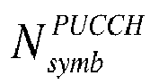
PUCCH format 2, and
PUCCH format 2;
and/or, - determining NRE as

PUCCH format 3/4 is used to transmit the first UCI, wherein
PUCCH format 3/4,
PUCCH format 3/4, and
format 3/4. - In a possible implementation, g(OUCI /NRE) is a linear fitting function with Ouci and NRE being variables.
- In a possible implementation, g(OUCI /NRE) is a*(OUCI/NRE) + b, wherein a and b are tuning coefficients, 1.5≤a≤2.5, and -1≤b≤1.
- In a possible implementation, a and b include a plurality of preset values respectively, and the processor determines the offset ΔPUCCH_TF,c(i) for PUCCH power control caulculation according to the formula ΔPUCCH_TF,c (i) = 10log10 (2 g(OUCI /NRE ) -1) by:
determining values of a and b corresponding to a PUCCH format used for transmitting the first UCI, the Ouci of the first UCI, and a frequency hopping situation. - In a third aspect, a terminal is provided, which includes:
- a first determining module configured to determine a quantity Ouci of bits of first UCI required to be transmitted on a PUCCH, and determine a quantity NRE of REs bearing the first UCI in the PUCCH;
- a second determining module configured to determine an offset ΔPUCCH_TF,c(i) for PUCCH power control calculation according to a formula ΔPUCCH_TF,c (i) = 10log10 (2 g(OUCI /NRE ) -1), wherein g(OUCI /NRE) is a function with Ouci and NRE being variables.
- In a possible implementation, the first determining module is configured to:
- determine NRE as

PUCCH format 2 is used to transmit the first UCI, wherein
PUCCH format 2, and
PUCCH format 2;
and/or, - determine NRE as

PUCCH format 3/4 is used to transmit the first UCI, wherein
PUCCH format 3/4,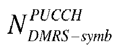
PUCCH format 3/4, and
format 3/4. - In a possible implementation, g(OUCI /NRE) is a linear fitting function with Ouci and NRE being variables.
- In a possible implementation, g(OUCI /NRE) is a*(OUCI/NRE) + b, wherein a and b are tuning coefficients, 1.5≤a≤2.5, and -1≤b≤1.
- In a possible implementation, a and b include a plurality of preset values respectively, and the second determining module is configured to:
determine values of a and b corresponding to a PUCCH format used for transmitting the first UCI, the Ouci of the first UCI, and a frequency hopping situation. - In a fourth aspect, a computer readable storage medium is provided.
- The computer readable storage medium stores computer instructions, which cause a computer device to perform the method as described in the first aspect when running on the computer device.
- In the embodiments of the present application, for determining the PUCCH power control offset, the quantity Ouci of bits of the first UCI required to be transmitted on the PUCCH is determined, and the quantity NRE of REs bearing the first UCI in the PUCCH is determined; and the offset ΔPUCCH_TF,c(i) for PUCCH power control calculation is determined according to the formula ΔPUCCH_TF,c (i) = 10log10(2 g(OUCI /NRE )-1) , wherein g(OUCI /NRE) is a function with Ouci and NRE being variables. Based on this solution, a new way to determine the PUCCH power control offset is provided. The test result shows that this solution can obtain the more accurate PUCCH power control offset, ensuring the transmission performance of the PUCCH channel in the new wireless communication system.
- In order to illustrate the embodiments of the present application or the technical solutions in the prior art more clearly, the accompanying figures which need to be used in describing the embodiments or the prior art will be introduced below briefly. Obviously the accompanying figures described below are some embodiments of the present application, and other accompanying figures can also be obtained by those ordinary skilled in the art according to the provided accompanying figures without creative labor.
-
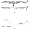
Fig. 1 is a schematic flowchart of a method for determining a PUCCH power control offset according to an embodiment of the present application; -
Fig. 2 is a schematic diagram of a terminal according to an embodiment of the present application; -
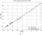
Fig. 3 is schematic diagram of a function g(OUCI /NRE) according to an embodiment of the present application; -
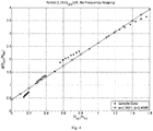
Fig. 4 is schematic diagram of a function g(OUCI /NRE) according to an embodiment of the present application; -
Fig. 5 is schematic diagram of a function g(OUCI /NRE) according to an embodiment of the present application. - In order to make the purposes, technical solutions and advantages of the embodiments of the present application clearer, the technical solutions in the embodiments of the present application will be described clearly and completely below in combination with the accompanying drawings in the embodiments of the present application. Obviously the described embodiments are a part of the embodiments of the present application but not all the embodiments. Based upon the embodiments of the present application, all of other embodiments obtained by those ordinary skilled in the art without creative work pertain to the protection scope of the present application.
- Furthermore, the term "and/or" herein is simply an association relationship describing the associated objects, indicating that there may be three relationships, for example, A and/or B may represent three conditions of: only A, both A and B, and only B. Furthermore, the character "/" herein generally indicates the "or" relationship of the front and back associated objects without special illustration. Furthermore, it should be understood that the word such as "first" or "second" in the description of the embodiments of the present application is only for purpose of distinguishing the description, and cannot be construed to indicate or imply the relative importance and cannot be construed to indicate or imply the order either.
- Firstly, the application scenarios and related knowledge of the embodiments of the present application will be introduced.
- In the LTE wireless communication system, the base station adjusts the power of the user terminal by way of open-loop and closed-loop power control, and the base station feeds back the power control information to the UE according to the UE uplink measurement result and adjusts the uplink transmit power obtained by the UE through the open-loop power control, and thus can control the transmit power of the UE more accurately.
- The LTE uses ΔTF,c(i) as a parameter in the calculation of the Physical Uplink Shared Channel (PUSCH) power, ΔTF,c(i) represents the offset related to the transmission format, and the calculation formula thereof is


- There is no definite solution for the definition of ΔPUHCC_TF,c(i) in the NR.
- Specifically, the PUCCH formats used in the LTE are different from the PUCCH formats in the NR. The NR supports 5 new PUCCH formats: the
PUCCH format 0 is a short PUCCH format of 2 bits or less; thePUCCH format 1 is a long PUCCH format of 2 bits or less; thePUCCH format 2 is a short PUCCH format of 2 bits or more; thePUCCH format 3 is a short PUCCH format of 2 bits or more and does not support multi-user multiplexing; and thePUCCH format 4 is a short PUCCH format of 2 bits or more and supports multi-user multiplexing. The TBCC coding is used in the LTE, and the coding combination scheme of CA-Polar and PC CA-Polar is used in the NR. In terms of performance, the performance of the NR scheme is much better than that of the LTE. Since the PUCCH formats, bit range, coding scheme, etc. used in the NR are all different, the reuse of ΔPUCCH_TF,c(i) in the LTE may reduce the transmission performance of the PUCCH in the NR. The offset used in the power control calculation performed for theNR PUCCH format 2/3/4 also needs to be different from that of LTE, to adapt to the new power control method and coding scheme in the NR. - The idea of the embodiments of the present application is to consider the calculation method of Signal to Noise Ratio (SNR) in the information theory. For the
PUCCH format 2 andPUCCH format 3/4 in the NR, by taking Ouci and NRE as the parameters, the corresponding formula form of ΔPUCCH_TF,c(i) and the value range applicable to the 5G Polar coding scheme are given. - The embodiment of the present application provides a method for determining a PUCCH power control offset, where the method can be applied to a terminal, e.g., a mobile phone, a tablet computer, a personal computer, a notebook computer, a wearable electronic device, and other devices with communication functions.
- Referring to
Fig. 1 , the process of the method for determining the PUCCH power control offset in the embodiment of the present application is described as follows. - Step 101: determining a quantity Ouci of bits of the first UCI required to be transmitted on a PUCCH, and determine a quantity NRE of REs bearing the first UCI in the PUCCH.
- Step 102: determining an offset ΔPUCCH_TF,c(i) for the PUCCH power control calculation according to a formula Δ PUCCH_TF,c (i) = 10log10(2 g(OUCI /NRE )-1), wherein g(OUCI /NRE) is a function with Ouci and NRE being variables.
- Here, Ouci may mean the number of bits of the CRC contained in the UCI.
- In a possible embodiment, the formula of calculating ΔPUCCH_TF,c(i) in some embodiments of the present application may be set to be used only in the case of Ouci > 17 bits.
- In an embodiment of the present application, for different PUCCH formats, the quantity NRE of REs bearing the first UCI in the PUCCH is determined in different ways.
- (1) For the
PUCCH format 2,
Here,
PUCCH format 2, and
PUCCH format 2. - (2) For the
PUCCH format 3,
Here,
PUCCH format 3,
PUCCH format 3, and
PUCCH format 3. - (3) For the
PUCCH format 4,
- Here,

PUCCH format 4,
PUCCH format 4, and
PUCCH format 4. - In other words, the way to determine NRE when using the
PUCCH format 2 to transmit the UCI is different from the way to determine NRE when using thePUCCH format 3/4 to transmit the UCI. That is, ΔPUCCH_TF,c(i) is calculated by using different parameters for thePUCCH format 2 andPUCCH format 3/4. - In a possible embodiment, g(OUCI /NRE) in the formula ΔPUCCH_TF,c (i) = 10 log10(2 g(OUCI /NRE ) -1) is a linear fitting function with OUCI and NRE being variables.
- For example, a possible expression of the linear fitting function g(O UCI/ NRE) is: a*(OUCI/NRE) + b, that is, g(OUCI /NRE) =a*(OUCI/NRE) + b in this case.
- Here, a and b are tuning coefficients which are preset values, where the value range of a may be [1.5, 2.5], and the value range of b may be [-1, 1], that is, 1.5≤a≤2.5, -1≤b≤1.
- Since the PUCCH format, the UCI length range and whether to use the frequency hopping may affect the transmission performance, the SNRs that meet the Block Error Rate (BLER) requirement are different. Thus, in the embodiments of the present application, different values of a and b may be used for different situations to reflect the impact of performance changes on the power control offset more accurately.
- According to the combinations of three conditions: PUCCH format, UCI length range and whether to use the frequency hopping (i.e., frequency modulation situation), 8 cases may be obtained, and the corresponding values of a and b may be preset for any one of these 8 cases. A possible correspondence is shown in Table 1:
Table 1 PUCCH format 2 3/4 Ouci 18≤OUCI≤25 OUCI>25 18≤OUCI≤25 OUCI> 25 whether to use frequency hopping Yes No Yes No Yes No Yes No Value of a a1 a2 a3 a4 a5 a6 a7 a8 Value of b b1 b2 b3 b4 b5 b6 b7 b8 - That is to say, in some embodiments of the present application, the correspondence among the PUCCH format, the UCI length range, the frequency hopping situation and the values of a and b may be preset. When ΔPUCCH_TF,c(i) used for transmitting the first UCI is calculated, there is only a need to determine the values of a and b corresponding to the PUCCH format, Ouci of the first UCI and the frequency hopping situation required to be used for transmitting the first UCI from a plurality of preset values included respectively in a and b according to the preset correspondence.
- In a possible embodiment, the formula ΔPUCCH_TF,c (i) = 10log10 (2 g( OUCI / NRE ) -1) and the preset values of a and b in the formula may be determined through simulation tests.
- For ease of understanding, the method for determining the PUCCH power control offset will be illustrated below by way of examples.
- Assuming a = 2.2902 and b = 0.1479 are set for
PUCCH format 2, 18 ≤ OUCI ≤ 25, and using frequency hopping, that is, a1 = 2.2902 and b1 = 0.1479 in Table 1 are set, then:
When the UE obtains Ouci = 18 and calculates NRE = 16 by using the parameters set by the upper layer, ΔPUCCH_TF,c(i) = 7.4887 may be calculated according to the formula ΔPUCCH_TF,c (i) = 10log10 (2 g(O UCI/ NRE ) -1) , that is, the power control offset suitable for the Polar code is obtained. - Refer to
Fig. 3 , it can be seen that the values of the function g(O UCI/ NRE) corresponding to different OUCI/NRE under such parameters are all relatively close to the set sample data. - Assuming a = 2.1871 and b = 0.4385 are set for
PUCCH format 2, 18 ≤ OUCI ≤ 25, and no frequency hopping, that is, a2 = 2.1871 and b2 = 0.4385 in Table 1 are set, then:
When the UE obtains Ouci = 20 and calculates NRE = 16 by using the parameters set by the upper layer, ΔPUCCH_TF,c(i) = 9.1727 may be calculated according to the formula Δ PUCCHTF,c (i) = 10log10 (2 g(O UCI/ NRE ) -1), that is, the power control offset suitable for the Polar code is obtained. - Refer to
Fig. 4 , it can be seen that the values of the function g(O UCI/ NRE) corresponding to different OUCI/NRE under such parameters are all relatively close to the set sample data. - Assuming a = 1.8746 and b = 0.5063 are set for
PUCCH format 3, Ouci ≥ 26 (i.e., OUCI > 25), and using frequency hopping, that is, a7 = 1.8746 and b7 = 0.5063 in Table 1 are set, then:
When the UE obtains Ouci = 32 and calculates NRE = 24 by using the parameters set by the upper layer, ΔPUCCH_TF,c(i) = 8.4791 may be calculated according to the formula ΔPUCCH_TF,c (i) = 10log10 (2 g(OUCI/ NRE ) -1), that is, the power control offset suitable for the Polar code is obtained. - Refer to
Fig. 5 , it can be seen that the values of the function g(O UCI/ NRE) corresponding to different OUCI/NRE under such parameters are all relatively close to the set sample data. - Based on the same inventive concept, an embodiment of the present application provides a terminal, which includes at least a memory and a processor, and is, for example, the terminal shown in
Fig. 2 . The terminal shown inFig. 2 includes amemory 201, aprocessor 202 and atransceiver 203, wherein thememory 201 and thetransceiver 203 may be connected to theprocessor 202 through a bus interface, or may be connected to theprocessor 202 through special connection lines; and thetransceiver 203 may be configured to receive the information sent by devices such as base stations, for example, receive the high-level signaling. - Here, the
memory 201 may be configured to store instructions, and theprocessor 202 may be configured to read the instructions in thememory 201 and perform the process of:
determining a quantity Ouci of bits of the first UCI required to be transmitted on a PUCCH, and determining a quantity NRE of REs bearing the first UCI in the PUCCH; and determining an offset ΔPUCCH_TF,c(i) for PUCCH power control calculation according to a formula ΔPUCCH_TF,c (i) = 10log10 (2 g(OUCI/ NRE) -1), wherein g(OUCI /NRE) is a function with Ouci and NRE being variables. - In a possible embodiment, the
processor 202 determines the quantity NRE of REs bearing the UCI in the PUCCH by: - determining NRE as

PUCCH format 2 is used to transmit the first UCI, wherein
PUCCH format 2, and
PUCCH format 2;
and/or, - determining NRE as

PUCCH format 3/4 is used to transmit the first UCI, wherein
PUCCH format 3/4,
PUCCH format 3/4, and
PUCCH format 3/4. - In a possible embodiment, g(OUCI /NRE) is a linear fitting function with Ouci and NRE being variables.
- In a possible embodiment, g(OUCI /NRE) is specifically a*(OUCI/NRE) + b, wherein a and b are tuning coefficients, 1.5≤a≤2.5, and -1≤b≤1.
- In a possible embodiment, a and b include a plurality of preset values respectively, and the
processor 202 determines the offset ΔPUCCH_TF,c(i) for the PUCCH power control calculation according to the formula ΔPUCCH_TF,c (i) = 10log10 (2 g( OUCI / NRE ) -1) by:
determining values of a and b corresponding to the PUCCH format used for transmitting the first UCI, the Ouci of the first UCI, and the frequency hopping situation. - Based on the same inventive concept, an embodiment of the present application provides a terminal, which includes a first determining module and a second determining module. In a specific implementation process, the first determining module and the second determining module may be an integral whole, or independent modules that can exchange the data with each other; and the first determining module and the second determining module may also be divided into a plurality of sub-modules, where each sub-module is used to implement specific functions of the first determining module or the second determining module.
- The first determining module is configured to determine a quantity Ouci of bits of the first UCI required to be transmitted on a PUCCH, and determine a quantity NRE of REs bearing the first UCI in the PUCCH;
- The second determining module is configured to determine an offset ΔPUCCH_TF,c(i) for PUCCH power control calculation according to a formula ΔPUCCH_TF,c (i) = 10 log10 (2 g( OUCI/ NRE ) -1), wherein g(OUCI /NRE) is a function with OUCI and NRE being variables.
- In a possible implementation, the first determining module is configured to:
- determine NRE as
PUCCH format 2 is used to transmit the first UCI, wherein
PUCCH format 2, and
PUCCH format 2;
and/or, - determine NRE as

PUCCH format 3/4 is used to transmit the first UCI, wherein
PUCCH format 3/4,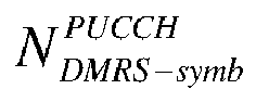
PUCCH format 3/4, and
PUCCH format 3/4. - In a possible implementation, g(OUCI /NRE) is a linear fitting function with Ouci and NRE being variables.
- In a possible implementation, g(OUCI /NRE) is specifically a*(OUCI/NRE) + b, wherein a and b are tuning coefficients, 1.5≤a≤2.5, and -1≤b≤1.
- In a possible implementation, a and b include a plurality of preset values respectively, and the second determining module is configured to:
determine values of a and b corresponding to the PUCCH format used for transmitting the first UCI, the Ouci of the first UCI, and the frequency hopping situation. - Based on the same inventive concept, an embodiment of the present application provides a computer readable storage medium storing the computer instructions, which cause a computer device to perform the method as described in the first embodiment when running on the computer device.
- In a specific implementation process, the computer readable storage medium includes: Universal Serial Bus (USB) flash drive, mobile hard disk, Read-Only Memory (ROM), Random Access Memory (RAM), magnetic disk or compact disc or various storage media that can store the program codes.
- One or more of the above-mentioned technical solutions have at least the following beneficial effects.
- In the embodiments of the present application, for calculating the PUCCH power control offset, the number Ouci of bits of the first UCI required to be transmitted on the PUCCH is determined, and the number NRE of REs bearing the first UCI in the PUCCH is determined; and the offset ΔPUCCH_TF,c(i) for the PUCCH power control calculation is determined according to the formula ΔPUCCH_TF,c (i) = 10log10 (2 g(OUCI /NRE ) -1), wherein g(OUCI /NRE) is a function with Ouci and NRE being variables. Based on this solution, a new way to determine the PUCCH power control offset is provided. The test result shows that this solution can obtain the more accurate PUCCH power control offset, ensuring the transmission performance of the PUCCH channel in the new wireless communication system.
- Further, different methods for determining NRE are used for the
PUCCH format 2 andPUCCH format 3/4, which can be more targeted and determine NRE more accurately, and thus obtain the more accurate PUCCH power control offset based on the determined NRE. - The device embodiments described above are merely illustrative, wherein the units/modules described as separate components may or may not be physically separated, and the components displayed as units/modules may or may not be physical units/modules, that is, may be located in one place or may be distributed onto multiple network units/modules. Some or all of the modules may be selected according to the actual needs to achieve the objects of the solutions of the embodiments. Those ordinary skilled in the art can understand and implement without creative labor.
- Through the above description of the embodiments, it is clear for those skilled in the art that the embodiments may be implemented by means of software plus the required general-purpose hardware platform, or of course, may be implemented by means of hardware. Based on such understanding, the above technical solution in itself or the part which contributes to the prior art can be embodied in the form of software product. The computer software product can be stored in the computer readable storage medium such as ROM/RAM, disk, compact disc or the like, and include a number of instructions used to enable a computer equipment (which can be personal computer, server, network equipment or the like) to perform the methods described in various embodiments or some parts of the embodiments.
- Finally, it should be noted that the above embodiments are only used to illustrate but not limit the technical solutions of the present application; although the present application has been illustrated in details by reference to the above embodiments, it should be understood by those ordinary skilled in the art that they can still modify the technical solutions recorded in all the above embodiments or equivalently replace some technical features therein; and these modifications and replacements do not make the essence of the corresponding technical solutions depart from the spirit and scope of the technical solutions of all the embodiments of the present application.
Claims (12)
- A method for determining a Physical Uplink Control Channel, PUCCH, power control offset, comprising:determining a quantity Ouci of bits of first Uplink Control Information, UCI, required to be transmitted on a PUCCH, and determining a quantity NRE of Resource Elements, REs, bearing the first UCI in the PUCCH; anddetermining the offset ΔPUCCH_TF,c(i) for PUCCH power control calculation according to a formula ΔPUCCH_TF,c (i) = 10log10 (2 g(O
UCI /NRE ) -1), wherein g(OUCI /NRE) is a function with Ouci and NRE being variables. - The method of claim 1, wherein the determining the quantity NRE of REs bearing the UCI in the PUCCH, comprises:determining NRE as


and/or,determining NRE as


- The method of claim 1 or 2, wherein g(OUCI /NRE) is a linear fitting function with Ouci and NRE being variables.
- The method of claim 3, wherein g(OUCI /NRE) is a*(OUCI/NRE) + b, wherein a and b are tuning coefficients, 1.5≤a≤2.5, and -1≤b≤1.
- The method of claim 4, wherein a and b comprise a plurality of preset values respectively, and the determining the offset ΔPUCCH_TF,c(i) for PUCCH power control calculation according to the formula ΔPUCCH_TF,c (i) = 10log10 (2 g(OUCI /NRE ) -1), comprises:
determining values of a and b corresponding to a PUCCH format used for transmitting the first UCI, the OUCI of the first UCI, and a frequency hopping situation. - A terminal, comprising:a memory configured to store instructions;a processor configured to read the instructions in the memory to:
determine a quantity Ouci of bits of first Uplink Control Information, UCI, required to be transmitted on a PUCCH, and determine a quantity NRE of Resource Elements, REs, bearing the first UCI in the PUCCH; and determine an offset ΔPUCH_TF,c(i) for PUCCH power control calculation according to a formula ΔPUCCH_TF,c (i) = 10log10(2 g(OUCI /N RE ) -1) , wherein g(OUCI /NRE) is a function with Ouci and NRE being variables. - The terminal of claim 6, wherein the processor determines the quantity NRE of REs bearing the UCI in the PUCCH by:determining NRE as


and/or,determining NRE as


- The terminal of claim 6 or 7, wherein g(OUCI /NRE) is a linear fitting function with Ouci and NRE being variables.
- The terminal of claim 8, wherein g(OUCI /NRE) is a*(OUCI/NRE) + b, wherein a and b are tuning coefficients, 1.5≤a≤2.5, and -1≤b≤1.
- The terminal of claim 9, wherein a and b comprise a plurality of preset values respectively, and the processor determines the offset ΔPUCCH_TF,c(i) for PUCCH power control calculation according to the formula ΔPUCCH_TF,c (i) = 10log10 (2 g(OUCI /N RE ) -1) by:
determining values of a and b corresponding to a PUCCH format used for transmitting the first UCI, the Ouci of the first UCI, and a frequency hopping situation. - A terminal, comprising:a first determining module configured to determine a quantity Ouci of bits of first Uplink Control Information, UCI, required to be transmitted on a PUCCH, and determine a quantity NRE of Resource Elements, REs, bearing the first UCI in the PUCCH;a second determining module configured to determine an offset ΔPUCCH_TF,c(i) for PUCCH power control calculation according to a formula ΔPUCCH_TF,c (i)=10log10(2 g(OUCI /N RE )-1), wherein g(OUCI /NRE) is a function with Ouci and NRE being variables.
- A computer readable storage medium storing computer instructions, wherein the computer instructions running on a computer device cause the computer device to perform the method of any one of claims 1-5.
Priority Applications (1)
| Application Number | Priority Date | Filing Date | Title |
|---|---|---|---|
| EP22213771.3A EP4178276A1 (en) | 2018-03-30 | 2018-12-05 | Determining power control offset for pucch |
Applications Claiming Priority (2)
| Application Number | Priority Date | Filing Date | Title |
|---|---|---|---|
| CN201810296910.7A CN110324887B (en) | 2018-03-30 | 2018-03-30 | Method and device for determining PUCCH power control offset |
| PCT/CN2018/119419 WO2019184431A1 (en) | 2018-03-30 | 2018-12-05 | Method and device for determining power control offset for pucch |
Related Child Applications (2)
| Application Number | Title | Priority Date | Filing Date |
|---|---|---|---|
| EP22213771.3A Division-Into EP4178276A1 (en) | 2018-03-30 | 2018-12-05 | Determining power control offset for pucch |
| EP22213771.3A Division EP4178276A1 (en) | 2018-03-30 | 2018-12-05 | Determining power control offset for pucch |
Publications (3)
| Publication Number | Publication Date |
|---|---|
| EP3780774A1 true EP3780774A1 (en) | 2021-02-17 |
| EP3780774A4 EP3780774A4 (en) | 2021-05-26 |
| EP3780774B1 EP3780774B1 (en) | 2023-02-15 |
Family
ID=68060913
Family Applications (2)
| Application Number | Title | Priority Date | Filing Date |
|---|---|---|---|
| EP22213771.3A Pending EP4178276A1 (en) | 2018-03-30 | 2018-12-05 | Determining power control offset for pucch |
| EP18912041.3A Active EP3780774B1 (en) | 2018-03-30 | 2018-12-05 | Method and device for determining power control offset for pucch |
Family Applications Before (1)
| Application Number | Title | Priority Date | Filing Date |
|---|---|---|---|
| EP22213771.3A Pending EP4178276A1 (en) | 2018-03-30 | 2018-12-05 | Determining power control offset for pucch |
Country Status (5)
| Country | Link |
|---|---|
| US (2) | US11540226B2 (en) |
| EP (2) | EP4178276A1 (en) |
| KR (1) | KR102358163B1 (en) |
| CN (1) | CN110324887B (en) |
| WO (1) | WO2019184431A1 (en) |
Family Cites Families (7)
| Publication number | Priority date | Publication date | Assignee | Title |
|---|---|---|---|---|
| CN101466138B (en) * | 2008-12-31 | 2011-04-06 | 华为技术有限公司 | Method, device and system for configuring power |
| CN102348269B (en) * | 2011-09-27 | 2015-01-28 | 电信科学技术研究院 | Method and device of uplink power control |
| US9876623B2 (en) * | 2014-12-22 | 2018-01-23 | Samsung Electronics Co., Ltd. | Transmission of uplink control information in carrier aggregation with a large number of cells |
| US9985742B2 (en) * | 2015-04-06 | 2018-05-29 | Samsung Electronics Co., Ltd. | Transmission power control for an uplink control channel |
| CN106257856B (en) * | 2015-06-19 | 2021-02-02 | 北京三星通信技术研究有限公司 | Method for transmitting uplink control information |
| CN107888267B (en) * | 2016-09-30 | 2023-11-10 | 华为技术有限公司 | Uplink power control method and device |
| CN109104761B (en) * | 2017-06-21 | 2020-08-18 | 维沃移动通信有限公司 | Information configuration method, power adjustment method, base station and mobile terminal |
-
2018
- 2018-03-30 CN CN201810296910.7A patent/CN110324887B/en active Active
- 2018-12-05 US US16/977,086 patent/US11540226B2/en active Active
- 2018-12-05 KR KR1020207030962A patent/KR102358163B1/en active Active
- 2018-12-05 EP EP22213771.3A patent/EP4178276A1/en active Pending
- 2018-12-05 EP EP18912041.3A patent/EP3780774B1/en active Active
- 2018-12-05 WO PCT/CN2018/119419 patent/WO2019184431A1/en not_active Ceased
-
2022
- 2022-11-24 US US17/993,974 patent/US12022403B2/en active Active
Also Published As
| Publication number | Publication date |
|---|---|
| KR20200135868A (en) | 2020-12-03 |
| KR102358163B1 (en) | 2022-02-08 |
| EP3780774B1 (en) | 2023-02-15 |
| US20230104435A1 (en) | 2023-04-06 |
| US12022403B2 (en) | 2024-06-25 |
| EP3780774A4 (en) | 2021-05-26 |
| US11540226B2 (en) | 2022-12-27 |
| CN110324887B (en) | 2021-07-23 |
| US20210007056A1 (en) | 2021-01-07 |
| EP4178276A1 (en) | 2023-05-10 |
| CN110324887A (en) | 2019-10-11 |
| WO2019184431A1 (en) | 2019-10-03 |
Similar Documents
| Publication | Publication Date | Title |
|---|---|---|
| US11470558B2 (en) | Uplink power control method, user equipment and base station | |
| US11330530B2 (en) | Power control method and terminal device | |
| EP4418762A2 (en) | Uplink power control method, terminal device, and network device | |
| EP3860019A1 (en) | Method for determining occupation time of channel state information (csi) processing unit, and terminal device | |
| CN110167126B (en) | Control method and device for PUCCH power during multi-beam transmission | |
| EP3852288A1 (en) | Power indication method and device | |
| US10602455B2 (en) | Power control method and apparatus for uplink control channel | |
| CN104619000B (en) | uplink power control method, system and related equipment | |
| EP2375827B9 (en) | A physical uplink shared channel transmission power control method and system | |
| EP3515130A1 (en) | Uplink power control method and apparatus | |
| EP3700279A1 (en) | Channel state information report transmission method and communication device | |
| CN109842929B (en) | Method and device for acquiring power control offset | |
| EP3531753A1 (en) | Uplink power control method and communication apparatus | |
| US11855726B2 (en) | Method and apparatus for determining transmit power | |
| US20230104435A1 (en) | Method and device for determining power control offset for pucch | |
| WO2022205093A1 (en) | Methods, apparatuses, and computer readable media for reporting and managing coverage enhancement level | |
| US20200374805A1 (en) | Uplink power control method and mobile terminal | |
| EP4578125B1 (en) | Handling of cqi reports in the presence of prb blocking | |
| EP4598199A1 (en) | Information determination method, apparatus, terminal and network device | |
| WO2024235554A1 (en) | Enhanced channel state information derivation | |
| EP3013106A1 (en) | Control information transmission method, user equipment and base station | |
| HK1158433B (en) | A physical uplink shared channel transmission power control method and system | |
| WO2015023297A1 (en) | Method and apparatus for mitigating relative-phase discontinuity |
Legal Events
| Date | Code | Title | Description |
|---|---|---|---|
| STAA | Information on the status of an ep patent application or granted ep patent |
Free format text: STATUS: THE INTERNATIONAL PUBLICATION HAS BEEN MADE |
|
| PUAI | Public reference made under article 153(3) epc to a published international application that has entered the european phase |
Free format text: ORIGINAL CODE: 0009012 |
|
| STAA | Information on the status of an ep patent application or granted ep patent |
Free format text: STATUS: REQUEST FOR EXAMINATION WAS MADE |
|
| 17P | Request for examination filed |
Effective date: 20200916 |
|
| AK | Designated contracting states |
Kind code of ref document: A1 Designated state(s): AL AT BE BG CH CY CZ DE DK EE ES FI FR GB GR HR HU IE IS IT LI LT LU LV MC MK MT NL NO PL PT RO RS SE SI SK SM TR |
|
| AX | Request for extension of the european patent |
Extension state: BA ME |
|
| A4 | Supplementary search report drawn up and despatched |
Effective date: 20210429 |
|
| RIC1 | Information provided on ipc code assigned before grant |
Ipc: H04W 52/14 20090101AFI20210422BHEP Ipc: H04W 52/36 20090101ALI20210422BHEP Ipc: H04W 52/32 20090101ALI20210422BHEP Ipc: H04L 5/00 20060101ALN20210422BHEP |
|
| DAV | Request for validation of the european patent (deleted) | ||
| DAX | Request for extension of the european patent (deleted) | ||
| RAP1 | Party data changed (applicant data changed or rights of an application transferred) |
Owner name: DATANG MOBILE COMMUNICATIONS EQUIPMENT CO., LTD. |
|
| STAA | Information on the status of an ep patent application or granted ep patent |
Free format text: STATUS: EXAMINATION IS IN PROGRESS |
|
| 17Q | First examination report despatched |
Effective date: 20220208 |
|
| GRAP | Despatch of communication of intention to grant a patent |
Free format text: ORIGINAL CODE: EPIDOSNIGR1 |
|
| STAA | Information on the status of an ep patent application or granted ep patent |
Free format text: STATUS: GRANT OF PATENT IS INTENDED |
|
| RIC1 | Information provided on ipc code assigned before grant |
Ipc: H04B 1/713 20110101ALN20220801BHEP Ipc: H04L 5/00 20060101ALN20220801BHEP Ipc: H04W 52/36 20090101ALI20220801BHEP Ipc: H04W 52/32 20090101ALI20220801BHEP Ipc: H04W 52/14 20090101AFI20220801BHEP |
|
| INTG | Intention to grant announced |
Effective date: 20220902 |
|
| GRAS | Grant fee paid |
Free format text: ORIGINAL CODE: EPIDOSNIGR3 |
|
| GRAA | (expected) grant |
Free format text: ORIGINAL CODE: 0009210 |
|
| STAA | Information on the status of an ep patent application or granted ep patent |
Free format text: STATUS: THE PATENT HAS BEEN GRANTED |
|
| AK | Designated contracting states |
Kind code of ref document: B1 Designated state(s): AL AT BE BG CH CY CZ DE DK EE ES FI FR GB GR HR HU IE IS IT LI LT LU LV MC MK MT NL NO PL PT RO RS SE SI SK SM TR |
|
| REG | Reference to a national code |
Ref country code: CH Ref legal event code: EP Ref country code: GB Ref legal event code: FG4D |
|
| REG | Reference to a national code |
Ref country code: DE Ref legal event code: R096 Ref document number: 602018046289 Country of ref document: DE |
|
| REG | Reference to a national code |
Ref country code: AT Ref legal event code: REF Ref document number: 1548907 Country of ref document: AT Kind code of ref document: T Effective date: 20230315 Ref country code: IE Ref legal event code: FG4D |
|
| REG | Reference to a national code |
Ref country code: LT Ref legal event code: MG9D |
|
| P01 | Opt-out of the competence of the unified patent court (upc) registered |
Effective date: 20230512 |
|
| REG | Reference to a national code |
Ref country code: NL Ref legal event code: MP Effective date: 20230215 |
|
| REG | Reference to a national code |
Ref country code: AT Ref legal event code: MK05 Ref document number: 1548907 Country of ref document: AT Kind code of ref document: T Effective date: 20230215 |
|
| PG25 | Lapsed in a contracting state [announced via postgrant information from national office to epo] |
Ref country code: RS Free format text: LAPSE BECAUSE OF FAILURE TO SUBMIT A TRANSLATION OF THE DESCRIPTION OR TO PAY THE FEE WITHIN THE PRESCRIBED TIME-LIMIT Effective date: 20230215 Ref country code: PT Free format text: LAPSE BECAUSE OF FAILURE TO SUBMIT A TRANSLATION OF THE DESCRIPTION OR TO PAY THE FEE WITHIN THE PRESCRIBED TIME-LIMIT Effective date: 20230615 Ref country code: NO Free format text: LAPSE BECAUSE OF FAILURE TO SUBMIT A TRANSLATION OF THE DESCRIPTION OR TO PAY THE FEE WITHIN THE PRESCRIBED TIME-LIMIT Effective date: 20230515 Ref country code: NL Free format text: LAPSE BECAUSE OF FAILURE TO SUBMIT A TRANSLATION OF THE DESCRIPTION OR TO PAY THE FEE WITHIN THE PRESCRIBED TIME-LIMIT Effective date: 20230215 Ref country code: LV Free format text: LAPSE BECAUSE OF FAILURE TO SUBMIT A TRANSLATION OF THE DESCRIPTION OR TO PAY THE FEE WITHIN THE PRESCRIBED TIME-LIMIT Effective date: 20230215 Ref country code: LT Free format text: LAPSE BECAUSE OF FAILURE TO SUBMIT A TRANSLATION OF THE DESCRIPTION OR TO PAY THE FEE WITHIN THE PRESCRIBED TIME-LIMIT Effective date: 20230215 Ref country code: HR Free format text: LAPSE BECAUSE OF FAILURE TO SUBMIT A TRANSLATION OF THE DESCRIPTION OR TO PAY THE FEE WITHIN THE PRESCRIBED TIME-LIMIT Effective date: 20230215 Ref country code: ES Free format text: LAPSE BECAUSE OF FAILURE TO SUBMIT A TRANSLATION OF THE DESCRIPTION OR TO PAY THE FEE WITHIN THE PRESCRIBED TIME-LIMIT Effective date: 20230215 Ref country code: AT Free format text: LAPSE BECAUSE OF FAILURE TO SUBMIT A TRANSLATION OF THE DESCRIPTION OR TO PAY THE FEE WITHIN THE PRESCRIBED TIME-LIMIT Effective date: 20230215 |
|
| PG25 | Lapsed in a contracting state [announced via postgrant information from national office to epo] |
Ref country code: SE Free format text: LAPSE BECAUSE OF FAILURE TO SUBMIT A TRANSLATION OF THE DESCRIPTION OR TO PAY THE FEE WITHIN THE PRESCRIBED TIME-LIMIT Effective date: 20230215 Ref country code: PL Free format text: LAPSE BECAUSE OF FAILURE TO SUBMIT A TRANSLATION OF THE DESCRIPTION OR TO PAY THE FEE WITHIN THE PRESCRIBED TIME-LIMIT Effective date: 20230215 Ref country code: IS Free format text: LAPSE BECAUSE OF FAILURE TO SUBMIT A TRANSLATION OF THE DESCRIPTION OR TO PAY THE FEE WITHIN THE PRESCRIBED TIME-LIMIT Effective date: 20230615 Ref country code: GR Free format text: LAPSE BECAUSE OF FAILURE TO SUBMIT A TRANSLATION OF THE DESCRIPTION OR TO PAY THE FEE WITHIN THE PRESCRIBED TIME-LIMIT Effective date: 20230516 Ref country code: FI Free format text: LAPSE BECAUSE OF FAILURE TO SUBMIT A TRANSLATION OF THE DESCRIPTION OR TO PAY THE FEE WITHIN THE PRESCRIBED TIME-LIMIT Effective date: 20230215 |
|
| PG25 | Lapsed in a contracting state [announced via postgrant information from national office to epo] |
Ref country code: SM Free format text: LAPSE BECAUSE OF FAILURE TO SUBMIT A TRANSLATION OF THE DESCRIPTION OR TO PAY THE FEE WITHIN THE PRESCRIBED TIME-LIMIT Effective date: 20230215 Ref country code: RO Free format text: LAPSE BECAUSE OF FAILURE TO SUBMIT A TRANSLATION OF THE DESCRIPTION OR TO PAY THE FEE WITHIN THE PRESCRIBED TIME-LIMIT Effective date: 20230215 Ref country code: DK Free format text: LAPSE BECAUSE OF FAILURE TO SUBMIT A TRANSLATION OF THE DESCRIPTION OR TO PAY THE FEE WITHIN THE PRESCRIBED TIME-LIMIT Effective date: 20230215 Ref country code: CZ Free format text: LAPSE BECAUSE OF FAILURE TO SUBMIT A TRANSLATION OF THE DESCRIPTION OR TO PAY THE FEE WITHIN THE PRESCRIBED TIME-LIMIT Effective date: 20230215 |
|
| REG | Reference to a national code |
Ref country code: DE Ref legal event code: R097 Ref document number: 602018046289 Country of ref document: DE |
|
| PG25 | Lapsed in a contracting state [announced via postgrant information from national office to epo] |
Ref country code: SK Free format text: LAPSE BECAUSE OF FAILURE TO SUBMIT A TRANSLATION OF THE DESCRIPTION OR TO PAY THE FEE WITHIN THE PRESCRIBED TIME-LIMIT Effective date: 20230215 |
|
| PLBE | No opposition filed within time limit |
Free format text: ORIGINAL CODE: 0009261 |
|
| STAA | Information on the status of an ep patent application or granted ep patent |
Free format text: STATUS: NO OPPOSITION FILED WITHIN TIME LIMIT |
|
| 26N | No opposition filed |
Effective date: 20231116 |
|
| PG25 | Lapsed in a contracting state [announced via postgrant information from national office to epo] |
Ref country code: SI Free format text: LAPSE BECAUSE OF FAILURE TO SUBMIT A TRANSLATION OF THE DESCRIPTION OR TO PAY THE FEE WITHIN THE PRESCRIBED TIME-LIMIT Effective date: 20230215 |
|
| PG25 | Lapsed in a contracting state [announced via postgrant information from national office to epo] |
Ref country code: IT Free format text: LAPSE BECAUSE OF FAILURE TO SUBMIT A TRANSLATION OF THE DESCRIPTION OR TO PAY THE FEE WITHIN THE PRESCRIBED TIME-LIMIT Effective date: 20230215 |
|
| REG | Reference to a national code |
Ref country code: CH Ref legal event code: PL |
|
| PG25 | Lapsed in a contracting state [announced via postgrant information from national office to epo] |
Ref country code: LU Free format text: LAPSE BECAUSE OF NON-PAYMENT OF DUE FEES Effective date: 20231205 |
|
| PG25 | Lapsed in a contracting state [announced via postgrant information from national office to epo] |
Ref country code: MC Free format text: LAPSE BECAUSE OF FAILURE TO SUBMIT A TRANSLATION OF THE DESCRIPTION OR TO PAY THE FEE WITHIN THE PRESCRIBED TIME-LIMIT Effective date: 20230215 |
|
| REG | Reference to a national code |
Ref country code: BE Ref legal event code: MM Effective date: 20231231 |
|
| PG25 | Lapsed in a contracting state [announced via postgrant information from national office to epo] |
Ref country code: MC Free format text: LAPSE BECAUSE OF FAILURE TO SUBMIT A TRANSLATION OF THE DESCRIPTION OR TO PAY THE FEE WITHIN THE PRESCRIBED TIME-LIMIT Effective date: 20230215 Ref country code: LU Free format text: LAPSE BECAUSE OF NON-PAYMENT OF DUE FEES Effective date: 20231205 |
|
| REG | Reference to a national code |
Ref country code: IE Ref legal event code: MM4A |
|
| PG25 | Lapsed in a contracting state [announced via postgrant information from national office to epo] |
Ref country code: IE Free format text: LAPSE BECAUSE OF NON-PAYMENT OF DUE FEES Effective date: 20231205 |
|
| PG25 | Lapsed in a contracting state [announced via postgrant information from national office to epo] |
Ref country code: BE Free format text: LAPSE BECAUSE OF NON-PAYMENT OF DUE FEES Effective date: 20231231 |
|
| PG25 | Lapsed in a contracting state [announced via postgrant information from national office to epo] |
Ref country code: CH Free format text: LAPSE BECAUSE OF NON-PAYMENT OF DUE FEES Effective date: 20231231 |
|
| PG25 | Lapsed in a contracting state [announced via postgrant information from national office to epo] |
Ref country code: IE Free format text: LAPSE BECAUSE OF NON-PAYMENT OF DUE FEES Effective date: 20231205 Ref country code: CH Free format text: LAPSE BECAUSE OF NON-PAYMENT OF DUE FEES Effective date: 20231231 Ref country code: BE Free format text: LAPSE BECAUSE OF NON-PAYMENT OF DUE FEES Effective date: 20231231 |
|
| PG25 | Lapsed in a contracting state [announced via postgrant information from national office to epo] |
Ref country code: BG Free format text: LAPSE BECAUSE OF FAILURE TO SUBMIT A TRANSLATION OF THE DESCRIPTION OR TO PAY THE FEE WITHIN THE PRESCRIBED TIME-LIMIT Effective date: 20230215 |
|
| PG25 | Lapsed in a contracting state [announced via postgrant information from national office to epo] |
Ref country code: BG Free format text: LAPSE BECAUSE OF FAILURE TO SUBMIT A TRANSLATION OF THE DESCRIPTION OR TO PAY THE FEE WITHIN THE PRESCRIBED TIME-LIMIT Effective date: 20230215 |
|
| PG25 | Lapsed in a contracting state [announced via postgrant information from national office to epo] |
Ref country code: EE Free format text: LAPSE BECAUSE OF FAILURE TO SUBMIT A TRANSLATION OF THE DESCRIPTION OR TO PAY THE FEE WITHIN THE PRESCRIBED TIME-LIMIT Effective date: 20230215 |
|
| PG25 | Lapsed in a contracting state [announced via postgrant information from national office to epo] |
Ref country code: CY Free format text: LAPSE BECAUSE OF FAILURE TO SUBMIT A TRANSLATION OF THE DESCRIPTION OR TO PAY THE FEE WITHIN THE PRESCRIBED TIME-LIMIT; INVALID AB INITIO Effective date: 20181205 |
|
| PG25 | Lapsed in a contracting state [announced via postgrant information from national office to epo] |
Ref country code: HU Free format text: LAPSE BECAUSE OF FAILURE TO SUBMIT A TRANSLATION OF THE DESCRIPTION OR TO PAY THE FEE WITHIN THE PRESCRIBED TIME-LIMIT; INVALID AB INITIO Effective date: 20181205 |
|
| PG25 | Lapsed in a contracting state [announced via postgrant information from national office to epo] |
Ref country code: TR Free format text: LAPSE BECAUSE OF FAILURE TO SUBMIT A TRANSLATION OF THE DESCRIPTION OR TO PAY THE FEE WITHIN THE PRESCRIBED TIME-LIMIT Effective date: 20230215 |
|
| PGFP | Annual fee paid to national office [announced via postgrant information from national office to epo] |
Ref country code: DE Payment date: 20251211 Year of fee payment: 8 |
|
| PGFP | Annual fee paid to national office [announced via postgrant information from national office to epo] |
Ref country code: GB Payment date: 20251219 Year of fee payment: 8 |
|
| PGFP | Annual fee paid to national office [announced via postgrant information from national office to epo] |
Ref country code: FR Payment date: 20251229 Year of fee payment: 8 |