EP3780390A1 - Distributed amplifier - Google Patents
Distributed amplifier Download PDFInfo
- Publication number
- EP3780390A1 EP3780390A1 EP18917811.4A EP18917811A EP3780390A1 EP 3780390 A1 EP3780390 A1 EP 3780390A1 EP 18917811 A EP18917811 A EP 18917811A EP 3780390 A1 EP3780390 A1 EP 3780390A1
- Authority
- EP
- European Patent Office
- Prior art keywords
- distributed amplifier
- capacitor
- transmission line
- gate
- crlh
- Prior art date
- Legal status (The legal status is an assumption and is not a legal conclusion. Google has not performed a legal analysis and makes no representation as to the accuracy of the status listed.)
- Granted
Links
Images


Classifications
-
- H—ELECTRICITY
- H03—ELECTRONIC CIRCUITRY
- H03F—AMPLIFIERS
- H03F3/00—Amplifiers with only discharge tubes or only semiconductor devices as amplifying elements
- H03F3/60—Amplifiers in which coupling networks have distributed constants, e.g. with waveguide resonators
- H03F3/605—Distributed amplifiers
- H03F3/607—Distributed amplifiers using FET's
-
- H—ELECTRICITY
- H03—ELECTRONIC CIRCUITRY
- H03F—AMPLIFIERS
- H03F1/00—Details of amplifiers with only discharge tubes, only semiconductor devices or only unspecified devices as amplifying elements
- H03F1/08—Modifications of amplifiers to reduce detrimental influences of internal impedances of amplifying elements
- H03F1/18—Modifications of amplifiers to reduce detrimental influences of internal impedances of amplifying elements by use of distributed coupling, i.e. distributed amplifiers
-
- H—ELECTRICITY
- H03—ELECTRONIC CIRCUITRY
- H03F—AMPLIFIERS
- H03F1/00—Details of amplifiers with only discharge tubes, only semiconductor devices or only unspecified devices as amplifying elements
- H03F1/42—Modifications of amplifiers to extend the bandwidth
-
- H—ELECTRICITY
- H03—ELECTRONIC CIRCUITRY
- H03F—AMPLIFIERS
- H03F1/00—Details of amplifiers with only discharge tubes, only semiconductor devices or only unspecified devices as amplifying elements
- H03F1/56—Modifications of input or output impedances, not otherwise provided for
- H03F1/565—Modifications of input or output impedances, not otherwise provided for using inductive elements
-
- H—ELECTRICITY
- H03—ELECTRONIC CIRCUITRY
- H03F—AMPLIFIERS
- H03F3/00—Amplifiers with only discharge tubes or only semiconductor devices as amplifying elements
- H03F3/189—High-frequency amplifiers, e.g. radio frequency amplifiers
- H03F3/19—High-frequency amplifiers, e.g. radio frequency amplifiers with semiconductor devices only
- H03F3/195—High-frequency amplifiers, e.g. radio frequency amplifiers with semiconductor devices only in integrated circuits
-
- H—ELECTRICITY
- H03—ELECTRONIC CIRCUITRY
- H03F—AMPLIFIERS
- H03F2200/00—Indexing scheme relating to amplifiers
- H03F2200/225—Indexing scheme relating to amplifiers the input circuit of an amplifying stage comprising an LC-network
-
- H—ELECTRICITY
- H03—ELECTRONIC CIRCUITRY
- H03F—AMPLIFIERS
- H03F2200/00—Indexing scheme relating to amplifiers
- H03F2200/246—A series resonance being added in shunt in the input circuit, e.g. base, gate, of an amplifier stage, e.g. as a trap
-
- H—ELECTRICITY
- H03—ELECTRONIC CIRCUITRY
- H03F—AMPLIFIERS
- H03F2200/00—Indexing scheme relating to amplifiers
- H03F2200/36—Indexing scheme relating to amplifiers the amplifier comprising means for increasing the bandwidth
-
- H—ELECTRICITY
- H03—ELECTRONIC CIRCUITRY
- H03F—AMPLIFIERS
- H03F2200/00—Indexing scheme relating to amplifiers
- H03F2200/543—A transmission line being used as coupling element between two amplifying stages
-
- H—ELECTRICITY
- H03—ELECTRONIC CIRCUITRY
- H03F—AMPLIFIERS
- H03F3/00—Amplifiers with only discharge tubes or only semiconductor devices as amplifying elements
- H03F3/60—Amplifiers in which coupling networks have distributed constants, e.g. with waveguide resonators
- H03F3/605—Distributed amplifiers
Definitions
- the present invention relates to a distributed amplifier that is one of high frequency amplifiers for amplifying high frequency signals transmitted and received by, for example, a wireless communication device, a radar device, or the like.
- a high frequency amplifier for amplifying a high frequency signal is mounted on a wireless communication device, a radar device, or the like.
- a wireless communication device for example, there is one in which a source-grounded field effect transistor (FET) and a matching circuit are combined.
- FET field effect transistor
- the high frequency amplifier is required to have a high gain characteristic over a wide band.
- a general distributed amplifier includes a transistor arranged in parallel to each other and a transmission line.
- a combination of an inductance due to the transmission line disposed on the gate side of the transistor and a gate-source capacitor is regarded as a gate side pseudo transmission line.
- a combination of an inductance due to the transmission line disposed on the drain side and a drain-source capacitor of the transistor is regarded as a drain side pseudo transmission line.
- the distributed amplifier can obtain a wide band characteristic by implementing an arbitrary characteristic impedance regardless of frequency by the above-described pseudo transmission lines. Although the distributed amplifier has a wide band, when the transistor size is increased to increase the output, the upper limit frequency of the operation is limited by the cutoff frequency of the gate side pseudo transmission line due to a large gate-source capacitance.
- Non-Patent Literature 1 a technique has been used in which a capacitor is loaded in series with the gate-source capacitor and in a form of a shunt connection to the inductance (see Non-Patent Literature 1, for example).
- a shunt capacitance of the transmission line is small because the gate-source capacitor and the above-described capacitor are connected together in series, and as a result, the cutoff frequency can be increased.
- Non-Patent Literature 1 C. Campbell, "A Wideband Power Amplifier MMIC Utilizing GaN on SiC HEMT Technology," IEEE J. Solid-State Circuits, vol. 44, no. 10, pp. 2640-2647, Oct. 2009 .
- the present invention has been made to solve the problem as described above, and an object thereof is to provide a distributed amplifier capable of suppressing a decrease in gain and increasing the cutoff frequency.
- a distributed amplifier includes: a plurality of transistors connected in parallel to each other; and either or both an inductor shunt-connected to a transmission line on a control terminal side of at least one of the plurality of transistors and a capacitor connected in series to the transmission line on the control terminal side.
- the distributed amplifier of the present invention includes at least one of the inductor shunt-connected, or the capacitor connected in series, to the transmission line on the control terminal side of the transistor. As a result, it is possible to suppress the decrease in gain and increase the cutoff frequency.
- FIG. 1 is a configuration diagram illustrating an equivalent circuit of a distributed amplifier according to the present embodiment.
- the distributed amplifier illustrated in FIG. 1 includes an input terminal 1, an output terminal 2, FETs 3a to 3d, gate side transmission lines 4a to 4e, drain side transmission lines 5a to 5d, left-handed series capacitors 6a to 6d, left-handed shunt inductors 7a to 7d, DC cut capacitors 8a to 8e, and a gate side terminating resistor 9.
- the input terminal 1 is connected via the gate side transmission line 4a and the left-handed series capacitor 6a to the gate terminal of the FET 3a, and also to the left-handed shunt inductor 7a, the DC cut capacitor 8a, and the gate side transmission line 4b.
- the gate side transmission line 4a and the left-handed series capacitor 6a, and a gate-source capacitor of the FET 3a and the left-handed shunt inductor 7a form a CRLH line 10a. Similar structures form CRLH lines 10b to 10d.
- the CRLH lines 10a, 10b, 10c, and 10d are connected together in cascade, and the other end of the CRLH line 10d at the end is connected to the terminating resistor 9 and the DC cut capacitor 8e via the gate side transmission line 4e.
- the drain terminal of the FET 3a is connected to the drain terminal of the FET 3b and the drain side transmission line 5b via the drain side transmission line 5a.
- the other end of the drain side transmission line 5b is connected to the drain terminal of the FET 3c and the drain side transmission line 5c, and the other end of the drain side transmission line 5c is connected to the drain terminal of the FET 3d and the drain side transmission line 5d.
- the other end of the drain side transmission line 5d is connected to the output terminal 2.
- the source terminals of the FETs 3a to 3d are grounded to form a common terminal between the FETs 3a to 3d.
- the equivalent circuit is for a high frequency signal, and actually, gate and drain biases are supplied to the FET through gate and drain bias circuits that do not actually affect the high frequency signal.
- This configuration is implemented by using, for example, a Gallium Nitride (GaN) FET formed on a GaN Monolithic Microwave Integrated Circuit (MMIC), an inductance due to a metal wiring line, a capacitance of a Metal Insulator Metal (MIM) capacitor, and the like.
- GaN FET for example, a multi-finger transistor is used having a comb-tooth electrode structure in which drain fingers, gate fingers, and source fingers are alternately arranged.
- a high frequency signal is input from the input terminal 1 and distributed to the gate terminal of the FET 3a and the CRLH line 10b via the CRLH line 10a.
- the high frequency signal distributed to the CRLH line 10b is distributed to the gate terminal of the FET 3b and the CRLH line 10c.
- the high frequency signal distributed to the CRLH line 10c is distributed to the gate terminal of the FET 3c and the CRLH line 10d.
- the high frequency signal distributed to the CRLH line 10d is distributed to the gate terminal of the FET 3d and the terminating resistor 9.
- the high frequency signals distributed to the respective gate terminals of the FETs 3a to 3d are amplified and output to the respective drain terminals.
- the high frequency signal output from the drain terminal of the FET 3a is combined via the drain side transmission line 5a with the high frequency signal output from the drain terminal of the FET 3b.
- the combined signal from the drain terminals of the FETs 3a and 3b is combined via the drain side transmission line 5b with the high frequency signal output from the drain terminal of the FET 3c.
- This signal is further combined via the drain side transmission line 5c with the high frequency signal output from the drain terminal of the FET 3d, passes through the drain side transmission line 5d, and is output to the output terminal 2.
- FIG. 2 illustrates an equivalent circuit for RF of a unit cell of a gate side pseudo transmission line of the general distributed amplifier.
- an LC circuit including one transmission line and a gate-source capacitor of one FET is regarded as a unit cell.
- the input terminal 1 and an output terminal 11 indicate an input terminal and an output terminal of the unit cell.
- the DC cut capacitor loaded into the shunt inductor is omitted. A cutoff frequency of the unit cell of such a distributed amplifier is calculated.
- the voltage amplitude ratio is less than or equal to 1/A.
- Cr is a gate-source capacitor, and Lr is uniquely determined to set an impedance of the pseudo transmission line to a certain value such as 50 ⁇ .
- the cutoff frequency is uniquely determined.
- FIG. 3 illustrates an equivalent circuit for RF of a unit cell of a gate side pseudo transmission line of the distributed amplifier using a CRLH line in the distributed amplifier of the first embodiment.
- the DC cut capacitor loaded into the shunt inductor is omitted.
- a series inductance of the CRLH line is Lr
- a series capacitance is Cl
- a shunt inductance is Ll
- a shunt capacitance is Cr.
- the voltage amplitude ratio is less than or equal to 1/A.
- the cutoff frequency on the low frequency side can be arbitrarily determined by changing a value of ⁇ . Since an unnecessary low frequency signal that is not desired to be amplified is not passed, oscillation due to a loop via the transmission line or the bias circuit can be suppressed, so that there is also an effect that the low frequency signal can be easily stabilized.
- FIG 4 illustrates a calculation example.
- the voltage amplitude ratio is illustrated when a value of Cr and a pseudo transmission line impedance are made equal for the LC line and the CRLH line.
- a characteristic 401 illustrated by a solid line illustrates the pass amplitude of the LC line
- a characteristic 402 illustrated by a broken line illustrates the pass amplitude of the CRLH line.
- the cutoff frequency of the CRLH line is higher than that of the LC line.
- the plurality of transistors connected in parallel to each other, and at least one of the inductor shunt-connected to the transmission line on the control terminal side of at least one of the plurality of transistors or the capacitor connected in series to the transmission line on the control terminal side are provided, so that it is possible to suppress a decrease in gain and increase the cutoff frequency.
- a second embodiment is an example in which a capacitor is connected in series to a gate-source capacitor that is a capacitor between a control terminal and a common terminal of each of the FETs 3a to 3d.
- FIG. 5 illustrates an equivalent circuit of a distributed amplifier according to the second embodiment.
- Capacitors 12a to 12d are connected in series to the gate-source capacitors of the FETs 3a to 3d, respectively. That is, the capacitors 12a to 12d are shunt-connected to the gate side pseudo transmission lines of the FETs 3a to 3d. Since other configurations are similar to those of the first embodiment illustrated in FIG. 1 , corresponding portions are designated by the same reference numerals and description thereof will be omitted. Furthermore, the basic operation as the distributed amplifier is similar to that of the first embodiment.
- the CRLH lines 10a to 10d are configured by combining the CRLH structures with the capacitors 12a to 12d connected between the gate and the source, so that the cutoff frequency can be increased. Furthermore, when it is attempted to obtain the same cutoff frequency as that when a capacitor in series to the gate-source capacitor is loaded into the conventional LC line, since a capacitance value of the capacitor in series can be made larger in the configuration of the second embodiment, a divided voltage is reduced, and a decrease in gain can be suppressed.
- the pseudo transmission line is formed as the CRLH line, and then the capacitor is connected in series to the capacitor between the control terminal and the common terminal of each of the plurality of transistors, so that it is possible to suppress the decrease in gain due to voltage division and to increase the cutoff frequency more than when the pseudo transmission line is formed as the LC circuit.
- a third embodiment is an example in which an RC parallel circuit is connected in series to the gate-source capacitor of each of the FETs 3a to 3d.
- FIG. 6 illustrates an equivalent circuit of a distributed amplifier according to the third embodiment.
- Resistors 13a to 13d are connected in parallel to the capacitors 12a to 12d, respectively, and each form an RC parallel circuit.
- the configuration other than that is similar to that of the second embodiment illustrated in FIG. 5 .
- the basic operation as the distributed amplifier is similar to that of the second embodiment.
- an effect of stabilizing the low frequency signal is further obtained compared to the distributed amplifier of the second embodiment. That is, in general, FETs have lower stability factors at lower frequencies, and it is necessary to determine the specifications of the RC parallel circuits so that low frequencies can be sufficiently stabilized. For that reason, there has been a problem that the gain is reduced due to excessive stabilization at a frequency desired to be used, but the CRLH line itself has a small low frequency pass amplitude, so the need for stabilization by the RC parallel circuit is small, and there is an effect that excessive stabilization at the frequency desired to be used can be prevented when the CRLH line is used compared to when the conventional distributed amplifier using the LC line is used.
- the RC parallel circuit is connected in series to the capacitor between the control terminal and the common terminal of each of the plurality of transistors, so that stabilization of the low frequency signal can be further achieved in addition to the effects of the first embodiment.
- a fourth embodiment is an example in which the DC cut capacitors of the CRLH lines 10a to 10d are shared by the CRLH lines 10a to 10d.
- FIG. 7 illustrates an equivalent circuit of a distributed amplifier according to the fourth embodiment.
- DC cut capacitors 8f to 8h are capacitors commonly connected to the left-handed shunt inductors 7a to 7d. Since other configurations are similar to those of the first embodiment illustrated in FIG. 1 , corresponding portions are designated by the same reference numerals and description thereof will be omitted. Furthermore, the basic operation as the distributed amplifier is similar to that of the first embodiment.
- the gates of all the FETs 3a to 3d are connected together in a DC manner, so that a gate bias can be applied via each transmission line, and it is not necessary to separately provide gate bias circuits for the respective FETs 3a to 3d. Furthermore, an effect of simplifying the configuration can be obtained by DC cut sharing.
- the DC cut capacitor is connected to the shunt-connected inductor, and between the multiple inductors, connecting portions between the inductors and DC cut capacitors are connected together directly, so that in addition to the effects of the first embodiment, it is not necessary to separately provide the gate bias circuit for the FET, and the configuration can be simplified.
- a fifth embodiment is an example in which the left-handed shunt inductors 7a to 7d of the adjacent CRLH lines 10a to 10d are connected via a resistor.
- FIG. 8 illustrates an equivalent circuit of a distributed amplifier according to the fifth embodiment.
- a resistor 14a is a resistor connected between the left-handed shunt inductor 7a and the left-handed shunt inductor 7b
- a resistor 14b is a resistor connected between the left-handed shunt inductor 7b and the left-handed shunt inductor 7c
- a resistor 14c is a resistor connected between the left-handed shunt inductor 7c and the left-handed shunt inductor 7d. Since other configurations are similar to those of the first embodiment illustrated in FIG. 1 , corresponding portions are designated by the same reference numerals and description thereof will be omitted. Furthermore, the basic operation as the distributed amplifier is similar to that of the first embodiment.
- the adjacent left-handed shunt inductors 7a to 7d are connected via the resistors 14a to 14c.
- capacitance values of the DC cut capacitors 8f to 8h are set so that the DC cut capacitors 8f to 8h look like short circuits, and an effect of the resistor is made invisible.
- the DC cut capacitors 8f to 8h do not look like to be short-circuited sufficiently, and a stabilizing effect is obtained.
- the gate bias can be applied via each transmission line, so that if only one gate bias circuit is provided somewhere on the gate transmission line, there is no need to separately provide the gate bias circuits for the respective FETs 3a to 3d.
- the DC cut capacitor is connected to the shunt-connected inductor, and between the multiple inductors, connecting portions between the inductors and DC cut capacitors are connected together via the resistor, so that in addition to the effects of the first embodiment, it is not necessary to provide the gate bias circuits for the respective FETs, and the configuration can be simplified.
- a sixth embodiment is an example in which the DC cut capacitors 8a to 8e connected to the left-handed shunt inductors 7a to 7d of the CRLH lines 10a to 10d are replaced with diodes.
- FIG. 9 illustrates an equivalent circuit of a distributed amplifier according to the sixth embodiment.
- diodes 15a to 15d are diodes provided at positions of the DC cut capacitors 8a to 8e in the first embodiment illustrated in FIG. 1 . Since other configurations are similar to those of FIG. 1 , corresponding portions are designated by the same reference numerals and description thereof will be omitted.
- the basic operation as the distributed amplifier is similar to that of the first embodiment.
- a part of the drain finger of the comb-tooth electrode structure of the FET is installed without being connected to the output terminal, thereby being used as a diode.
- the diode is turned on and a current is generated, so that the FET can be protected.
- the cathode is grounded assuming GaN in which the gate bias applied to the gate is negative. The anode is grounded when the applied gate bias is positive.
- the diode for DC cut is connected to the shunt-connected inductor, so that effects can be obtained of stabilizing the low frequency signal and flattening the gain.
- the CRLH lines 10a to 10d are applied to all the gate side pseudo transmission lines, but they may be used only for some cells. Furthermore, the CRLH lines 10a to 10d are formed by using the left-handed shunt inductors 7a to 7d and the left-handed series capacitors 6a to 6d, but even when only the left-handed shunt inductors 7a to 7d or only the left-handed series capacitors 6a to 6d are used, it is possible to obtain the effect that the cutoff frequency can be increased.
- the CRLH lines 10a to 10d are applied to the gate side pseudo transmission line, but the CRLH lines 10a to 10d may be applied to the drain side pseudo transmission line or both the pseudo transmission lines. Moreover, as long as it is a distributed amplifier, a circuit change may be made such as the presence or absence of the terminating resistor.
- the number of FETs is four, but it can be arbitrarily changed.
- the GaN MMIC is taken as an example of the specific configuration of the distributed amplifier, the substrate material may be changed to GaAs or the like, or a structure using discrete components instead of the MMIC may be used.
- a bipolar transistor may be used instead of the FET.
- a uniformly distributed amplifier in which the impedances of all the pseudo transmission lines are equal is taken as an example, but the distributed amplifier may be a non-uniformly distributed amplifier that makes the impedances nonuniform for the purpose of improving the mismatch between the FET and the matching circuit.
- the distributed amplifier according to the present invention relates to the configuration in which the series-connected capacitor and the shunt inductor are used for the pseudo transmission line on the control terminal side, and is suitable for use in high frequency amplifiers for amplifying high frequency signals transmitted and received by a wireless communication device, a radar device, or the like.
Landscapes
- Engineering & Computer Science (AREA)
- Power Engineering (AREA)
- Microelectronics & Electronic Packaging (AREA)
- Microwave Amplifiers (AREA)
- Amplifiers (AREA)
Abstract
Description
- The present invention relates to a distributed amplifier that is one of high frequency amplifiers for amplifying high frequency signals transmitted and received by, for example, a wireless communication device, a radar device, or the like.
- A high frequency amplifier for amplifying a high frequency signal is mounted on a wireless communication device, a radar device, or the like. For example, there is one in which a source-grounded field effect transistor (FET) and a matching circuit are combined. The high frequency amplifier is required to have a high gain characteristic over a wide band.
- A general distributed amplifier includes a transistor arranged in parallel to each other and a transmission line. A combination of an inductance due to the transmission line disposed on the gate side of the transistor and a gate-source capacitor is regarded as a gate side pseudo transmission line. Furthermore, a combination of an inductance due to the transmission line disposed on the drain side and a drain-source capacitor of the transistor is regarded as a drain side pseudo transmission line. The distributed amplifier can obtain a wide band characteristic by implementing an arbitrary characteristic impedance regardless of frequency by the above-described pseudo transmission lines. Although the distributed amplifier has a wide band, when the transistor size is increased to increase the output, the upper limit frequency of the operation is limited by the cutoff frequency of the gate side pseudo transmission line due to a large gate-source capacitance. Thus, to increase the cutoff frequency, a technique has been used in which a capacitor is loaded in series with the gate-source capacitor and in a form of a shunt connection to the inductance (see
Non-Patent Literature 1, for example). A shunt capacitance of the transmission line is small because the gate-source capacitor and the above-described capacitor are connected together in series, and as a result, the cutoff frequency can be increased. - Non-Patent Literature 1: C. Campbell, "A Wideband Power Amplifier MMIC Utilizing GaN on SiC HEMT Technology," IEEE J. Solid-State Circuits, vol. 44, no. 10, pp. 2640-2647, Oct. 2009.
- However, in the above conventional distributed amplifier, there has been a problem that the voltage applied to the gate-source capacitor is divided by loading the capacitor in series with the gate-source capacitor, so that the gain is reduced.
- The present invention has been made to solve the problem as described above, and an object thereof is to provide a distributed amplifier capable of suppressing a decrease in gain and increasing the cutoff frequency.
- A distributed amplifier according to the present invention includes: a plurality of transistors connected in parallel to each other; and either or both an inductor shunt-connected to a transmission line on a control terminal side of at least one of the plurality of transistors and a capacitor connected in series to the transmission line on the control terminal side.
- The distributed amplifier of the present invention includes at least one of the inductor shunt-connected, or the capacitor connected in series, to the transmission line on the control terminal side of the transistor. As a result, it is possible to suppress the decrease in gain and increase the cutoff frequency.
-
-
FIG. 1 is a configuration diagram illustrating an equivalent circuit of a distributed amplifier according to a first embodiment of the present invention. -
FIG. 2 is an equivalent circuit diagram for RF of a unit cell of a gate side pseudo transmission line of a general distributed amplifier. -
FIG. 3 is an equivalent circuit diagram for RF of a unit cell of a gate side pseudo transmission line of the distributed amplifier according to the first embodiment of the present invention. -
FIG. 4 is an explanatory diagram illustrating pass characteristics of the gate side pseudo transmission line of the distributed amplifier according to the first embodiment of the present invention and a conventional distributed amplifier. -
FIG. 5 is a configuration diagram illustrating an equivalent circuit of a distributed amplifier according to a second embodiment of the present invention. -
FIG. 6 is a configuration diagram illustrating an equivalent circuit of a distributed amplifier according to a third embodiment of the present invention. -
FIG. 7 is a configuration diagram illustrating an equivalent circuit of a distributed amplifier according to a fourth embodiment of the present invention. -
FIG. 8 is a configuration diagram illustrating an equivalent circuit of a distributed amplifier according to a fifth embodiment of the present invention. -
FIG. 9 is a configuration diagram illustrating an equivalent circuit of a distributed amplifier according to a sixth embodiment of the present invention. - Hereinafter, to explain the present invention in more detail, embodiments for carrying out the present invention will be described with reference to the accompanying drawings.
-
FIG. 1 is a configuration diagram illustrating an equivalent circuit of a distributed amplifier according to the present embodiment. The distributed amplifier illustrated inFIG. 1 includes aninput terminal 1, anoutput terminal 2,FETs 3a to 3d, gateside transmission lines 4a to 4e, drainside transmission lines 5a to 5d, left-handed series capacitors 6a to 6d, left-handed shunt inductors 7a to 7d, DC cutcapacitors 8a to 8e, and a gateside terminating resistor 9. - The
input terminal 1 is connected via the gateside transmission line 4a and the left-handed series capacitor 6a to the gate terminal of theFET 3a, and also to the left-handed shunt inductor 7a, the DC cutcapacitor 8a, and the gateside transmission line 4b. The gateside transmission line 4a and the left-handed series capacitor 6a, and a gate-source capacitor of theFET 3a and the left-handed shunt inductor 7a form aCRLH line 10a. Similar structures formCRLH lines 10b to 10d. The CRLH lines 10a, 10b, 10c, and 10d are connected together in cascade, and the other end of theCRLH line 10d at the end is connected to the terminatingresistor 9 and the DC cutcapacitor 8e via the gateside transmission line 4e. The drain terminal of theFET 3a is connected to the drain terminal of theFET 3b and the drainside transmission line 5b via the drainside transmission line 5a. The other end of the drainside transmission line 5b is connected to the drain terminal of theFET 3c and the drainside transmission line 5c, and the other end of the drainside transmission line 5c is connected to the drain terminal of theFET 3d and the drainside transmission line 5d. The other end of the drainside transmission line 5d is connected to theoutput terminal 2. Furthermore, the source terminals of the FETs 3a to 3d are grounded to form a common terminal between the FETs 3a to 3d. - Note that, the equivalent circuit is for a high frequency signal, and actually, gate and drain biases are supplied to the FET through gate and drain bias circuits that do not actually affect the high frequency signal.
- This configuration is implemented by using, for example, a Gallium Nitride (GaN) FET formed on a GaN Monolithic Microwave Integrated Circuit (MMIC), an inductance due to a metal wiring line, a capacitance of a Metal Insulator Metal (MIM) capacitor, and the like. For the GaN FET, for example, a multi-finger transistor is used having a comb-tooth electrode structure in which drain fingers, gate fingers, and source fingers are alternately arranged.
- Next, the operation will be described of the distributed amplifier of the first embodiment.
- A high frequency signal is input from the
input terminal 1 and distributed to the gate terminal of theFET 3a and theCRLH line 10b via theCRLH line 10a. The high frequency signal distributed to theCRLH line 10b is distributed to the gate terminal of theFET 3b and theCRLH line 10c. The high frequency signal distributed to theCRLH line 10c is distributed to the gate terminal of theFET 3c and theCRLH line 10d. The high frequency signal distributed to theCRLH line 10d is distributed to the gate terminal of theFET 3d and the terminatingresistor 9. The high frequency signals distributed to the respective gate terminals of the FETs 3a to 3d are amplified and output to the respective drain terminals. The high frequency signal output from the drain terminal of theFET 3a is combined via the drainside transmission line 5a with the high frequency signal output from the drain terminal of theFET 3b. The combined signal from the drain terminals of theFETs side transmission line 5b with the high frequency signal output from the drain terminal of theFET 3c. This signal is further combined via the drainside transmission line 5c with the high frequency signal output from the drain terminal of theFET 3d, passes through the drainside transmission line 5d, and is output to theoutput terminal 2. - The principle of the first embodiment will be described in comparison with a general distributed amplifier.
FIG. 2 illustrates an equivalent circuit for RF of a unit cell of a gate side pseudo transmission line of the general distributed amplifier. In the gate side pseudo transmission line, an LC circuit including one transmission line and a gate-source capacitor of one FET is regarded as a unit cell. In the figure, theinput terminal 1 and anoutput terminal 11 indicate an input terminal and an output terminal of the unit cell. Furthermore, the DC cut capacitor loaded into the shunt inductor is omitted. A cutoff frequency of the unit cell of such a distributed amplifier is calculated. When a series inductance of the LC circuit is Lr and a shunt capacitance is Cr, a frequency at which a voltage amplitude ratio between input and output is 1/A is expressed as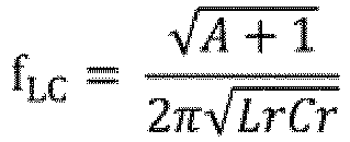
- At frequencies higher than the above cutoff frequency fLC, the voltage amplitude ratio is less than or equal to 1/A. Cr is a gate-source capacitor, and Lr is uniquely determined to set an impedance of the pseudo transmission line to a certain value such as 50 Ω. Thus, the cutoff frequency is uniquely determined.
-
FIG. 3 illustrates an equivalent circuit for RF of a unit cell of a gate side pseudo transmission line of the distributed amplifier using a CRLH line in the distributed amplifier of the first embodiment. The DC cut capacitor loaded into the shunt inductor is omitted. A series inductance of the CRLH line is Lr, a series capacitance is Cl, a shunt inductance is Ll, and a shunt capacitance is Cr. As a condition for not producing a band gap that cuts off a signal at a certain frequency on the CRLH line,
Ll = αLr
then, a cutoff frequency at which a voltage amplitude ratio between input and output of a CRLH line unit cell is 1/A is expressed as

- At frequencies lower than the above cutoff frequency fCRLH- and frequencies higher than fCRLH+, the voltage amplitude ratio is less than or equal to 1/A.
- Here,

thus, frequency bandwidths of the LC line and the CRLH line are equal. When the CRLH line is applied, the cutoff frequency is also generated on the low frequency side, but the cutoff frequency on the high frequency side can be made higher than that using the LC line. The cutoff frequency on the low frequency side can be arbitrarily determined by changing a value of α. Since an unnecessary low frequency signal that is not desired to be amplified is not passed, oscillation due to a loop via the transmission line or the bias circuit can be suppressed, so that there is also an effect that the low frequency signal can be easily stabilized. -
FIG 4 illustrates a calculation example. The voltage amplitude ratio is illustrated when a value of Cr and a pseudo transmission line impedance are made equal for the LC line and the CRLH line. In the figure, a characteristic 401 illustrated by a solid line illustrates the pass amplitude of the LC line, and a characteristic 402 illustrated by a broken line illustrates the pass amplitude of the CRLH line. As illustrated in the figure, it can be seen that the cutoff frequency of the CRLH line is higher than that of the LC line. - As described above, according to the distributed amplifier of the first embodiment, the plurality of transistors connected in parallel to each other, and at least one of the inductor shunt-connected to the transmission line on the control terminal side of at least one of the plurality of transistors or the capacitor connected in series to the transmission line on the control terminal side are provided, so that it is possible to suppress a decrease in gain and increase the cutoff frequency.
- A second embodiment is an example in which a capacitor is connected in series to a gate-source capacitor that is a capacitor between a control terminal and a common terminal of each of the FETs 3a to 3d.
-
FIG. 5 illustrates an equivalent circuit of a distributed amplifier according to the second embodiment.Capacitors 12a to 12d are connected in series to the gate-source capacitors of the FETs 3a to 3d, respectively. That is, thecapacitors 12a to 12d are shunt-connected to the gate side pseudo transmission lines of the FETs 3a to 3d. Since other configurations are similar to those of the first embodiment illustrated inFIG. 1 , corresponding portions are designated by the same reference numerals and description thereof will be omitted. Furthermore, the basic operation as the distributed amplifier is similar to that of the first embodiment. - In the distributed amplifier of the second embodiment, the CRLH lines 10a to 10d are configured by combining the CRLH structures with the
capacitors 12a to 12d connected between the gate and the source, so that the cutoff frequency can be increased. Furthermore, when it is attempted to obtain the same cutoff frequency as that when a capacitor in series to the gate-source capacitor is loaded into the conventional LC line, since a capacitance value of the capacitor in series can be made larger in the configuration of the second embodiment, a divided voltage is reduced, and a decrease in gain can be suppressed. - As described above, according to the distributed amplifier of the second embodiment, the pseudo transmission line is formed as the CRLH line, and then the capacitor is connected in series to the capacitor between the control terminal and the common terminal of each of the plurality of transistors, so that it is possible to suppress the decrease in gain due to voltage division and to increase the cutoff frequency more than when the pseudo transmission line is formed as the LC circuit.
- A third embodiment is an example in which an RC parallel circuit is connected in series to the gate-source capacitor of each of the FETs 3a to 3d.
-
FIG. 6 illustrates an equivalent circuit of a distributed amplifier according to the third embodiment.Resistors 13a to 13d are connected in parallel to thecapacitors 12a to 12d, respectively, and each form an RC parallel circuit. The configuration other than that is similar to that of the second embodiment illustrated inFIG. 5 . Furthermore, the basic operation as the distributed amplifier is similar to that of the second embodiment. - In the distributed amplifier of the third embodiment configured as described above, an effect of stabilizing the low frequency signal is further obtained compared to the distributed amplifier of the second embodiment. That is, in general, FETs have lower stability factors at lower frequencies, and it is necessary to determine the specifications of the RC parallel circuits so that low frequencies can be sufficiently stabilized. For that reason, there has been a problem that the gain is reduced due to excessive stabilization at a frequency desired to be used, but the CRLH line itself has a small low frequency pass amplitude, so the need for stabilization by the RC parallel circuit is small, and there is an effect that excessive stabilization at the frequency desired to be used can be prevented when the CRLH line is used compared to when the conventional distributed amplifier using the LC line is used.
- As described above, according to the distributed amplifier of the third embodiment, the RC parallel circuit is connected in series to the capacitor between the control terminal and the common terminal of each of the plurality of transistors, so that stabilization of the low frequency signal can be further achieved in addition to the effects of the first embodiment.
- A fourth embodiment is an example in which the DC cut capacitors of the CRLH lines 10a to 10d are shared by the CRLH lines 10a to 10d.
FIG. 7 illustrates an equivalent circuit of a distributed amplifier according to the fourth embodiment. InFIG. 7 , DC cutcapacitors 8f to 8h are capacitors commonly connected to the left-handed shunt inductors 7a to 7d. Since other configurations are similar to those of the first embodiment illustrated inFIG. 1 , corresponding portions are designated by the same reference numerals and description thereof will be omitted. Furthermore, the basic operation as the distributed amplifier is similar to that of the first embodiment. - In the distributed amplifier of the fourth embodiment configured as described above, by sharing the DC cut
capacitors 8f to 8h, the gates of all the FETs 3a to 3d are connected together in a DC manner, so that a gate bias can be applied via each transmission line, and it is not necessary to separately provide gate bias circuits for therespective FETs 3a to 3d. Furthermore, an effect of simplifying the configuration can be obtained by DC cut sharing. - As described above, according to the distributed amplifier of the fourth embodiment, the DC cut capacitor is connected to the shunt-connected inductor, and between the multiple inductors, connecting portions between the inductors and DC cut capacitors are connected together directly, so that in addition to the effects of the first embodiment, it is not necessary to separately provide the gate bias circuit for the FET, and the configuration can be simplified.
- A fifth embodiment is an example in which the left-
handed shunt inductors 7a to 7d of theadjacent CRLH lines 10a to 10d are connected via a resistor.FIG. 8 illustrates an equivalent circuit of a distributed amplifier according to the fifth embodiment. InFIG. 8 , aresistor 14a is a resistor connected between the left-handed shunt inductor 7a and the left-handed shunt inductor 7b, aresistor 14b is a resistor connected between the left-handed shunt inductor 7b and the left-handed shunt inductor 7c, and aresistor 14c is a resistor connected between the left-handed shunt inductor 7c and the left-handed shunt inductor 7d. Since other configurations are similar to those of the first embodiment illustrated inFIG. 1 , corresponding portions are designated by the same reference numerals and description thereof will be omitted. Furthermore, the basic operation as the distributed amplifier is similar to that of the first embodiment. - In the distributed amplifier of the fifth embodiment configured as described above, the adjacent left-
handed shunt inductors 7a to 7d are connected via theresistors 14a to 14c. For the frequency desired to be used, capacitance values of the DC cutcapacitors 8f to 8h are set so that the DC cutcapacitors 8f to 8h look like short circuits, and an effect of the resistor is made invisible. On the other hand, at low frequencies, the DC cutcapacitors 8f to 8h do not look like to be short-circuited sufficiently, and a stabilizing effect is obtained. Furthermore, since the gates of all the FETs 3a to 3d are connected together in a DC manner, the gate bias can be applied via each transmission line, so that if only one gate bias circuit is provided somewhere on the gate transmission line, there is no need to separately provide the gate bias circuits for therespective FETs 3a to 3d. - As described above, according to the distributed amplifier of the fifth embodiment, the DC cut capacitor is connected to the shunt-connected inductor, and between the multiple inductors, connecting portions between the inductors and DC cut capacitors are connected together via the resistor, so that in addition to the effects of the first embodiment, it is not necessary to provide the gate bias circuits for the respective FETs, and the configuration can be simplified.
- A sixth embodiment is an example in which the DC cut
capacitors 8a to 8e connected to the left-handed shunt inductors 7a to 7d of the CRLH lines 10a to 10d are replaced with diodes.FIG. 9 illustrates an equivalent circuit of a distributed amplifier according to the sixth embodiment. InFIG. 9 , diodes 15a to 15d are diodes provided at positions of the DC cutcapacitors 8a to 8e in the first embodiment illustrated inFIG. 1 . Since other configurations are similar to those ofFIG. 1 , corresponding portions are designated by the same reference numerals and description thereof will be omitted. Furthermore, the basic operation as the distributed amplifier is similar to that of the first embodiment. - In the distributed amplifier of the sixth embodiment configured as described above, a part of the drain finger of the comb-tooth electrode structure of the FET is installed without being connected to the output terminal, thereby being used as a diode. As a result, downsizing is possible even if the MIM capacitor is not used as the distributed amplifier. Furthermore, when a positive voltage due to static electricity or the like is applied to the input side, the diode is turned on and a current is generated, so that the FET can be protected. Note that, in the illustrated example, the cathode is grounded assuming GaN in which the gate bias applied to the gate is negative. The anode is grounded when the applied gate bias is positive.
- As described above, according to the distributed amplifier of the sixth embodiment, the diode for DC cut is connected to the shunt-connected inductor, so that effects can be obtained of stabilizing the low frequency signal and flattening the gain.
- Note that, in each of the above-described embodiments, the CRLH lines 10a to 10d are applied to all the gate side pseudo transmission lines, but they may be used only for some cells. Furthermore, the CRLH lines 10a to 10d are formed by using the left-
handed shunt inductors 7a to 7d and the left-handed series capacitors 6a to 6d, but even when only the left-handed shunt inductors 7a to 7d or only the left-handed series capacitors 6a to 6d are used, it is possible to obtain the effect that the cutoff frequency can be increased. - Furthermore, in each of the above-described embodiments, the CRLH lines 10a to 10d are applied to the gate side pseudo transmission line, but the CRLH lines 10a to 10d may be applied to the drain side pseudo transmission line or both the pseudo transmission lines. Moreover, as long as it is a distributed amplifier, a circuit change may be made such as the presence or absence of the terminating resistor.
- Furthermore, in each of the above-described embodiments, the number of FETs is four, but it can be arbitrarily changed. Moreover, although the GaN MMIC is taken as an example of the specific configuration of the distributed amplifier, the substrate material may be changed to GaAs or the like, or a structure using discrete components instead of the MMIC may be used. Furthermore, a bipolar transistor may be used instead of the FET.
- Furthermore, in each of the embodiments, a uniformly distributed amplifier in which the impedances of all the pseudo transmission lines are equal is taken as an example, but the distributed amplifier may be a non-uniformly distributed amplifier that makes the impedances nonuniform for the purpose of improving the mismatch between the FET and the matching circuit.
- In the invention of the present application, within the scope of the invention, free combination of the embodiments, a modification of an arbitrary component of the embodiments, or omission of an arbitrary component in the embodiments is possible.
- As described above, the distributed amplifier according to the present invention relates to the configuration in which the series-connected capacitor and the shunt inductor are used for the pseudo transmission line on the control terminal side, and is suitable for use in high frequency amplifiers for amplifying high frequency signals transmitted and received by a wireless communication device, a radar device, or the like.
-
- 1:
- input terminal,
- 2:
- output terminal,
- 3a to 3d:
- FET,
- 4a to 4e:
- gate side transmission line,
- 5a to 5d:
- drain side transmission line,
- 6a to 6d:
- left-handed series capacitor,
- 7a to 7d:
- left-handed shunt inductor,
- 8a to 8h:
- DC cut capacitor,
- 9:
- gate side terminating resistor,
- 12a to 12d:
- capacitor,
- 13a to 13d, 14a to 14c:
- resistor,
- 15a to 15d:
- diode
Claims (5)
- A distributed amplifier comprising:a plurality of transistors connected in parallel to each other; andeither or both an inductor shunt-connected to a transmission line on a control terminal side of at least one of the plurality of transistors and a capacitor connected in series to the transmission line on the control terminal side.
- The distributed amplifier according to claim 1, wherein a capacitor is connected in series to a capacitor between a control terminal and a common terminal of each of the plurality of transistors.
- The distributed amplifier according to claim 1, wherein an RC parallel circuit is connected in series to a capacitor between a control terminal and a common terminal of each of the plurality of transistors.
- The distributed amplifier according to any one of claims 1 to 3, wherein a DC cut capacitor is connected to the shunt-connected inductor, and between a plurality of inductors, connecting portions each between the inductor and the DC cut capacitor are connected together directly or via a resistor.
- The distributed amplifier according to any one of claims 1 to 3, wherein a diode for DC cut is connected to the shunt-connected inductor.
Applications Claiming Priority (1)
| Application Number | Priority Date | Filing Date | Title |
|---|---|---|---|
| PCT/JP2018/017964 WO2019215849A1 (en) | 2018-05-09 | 2018-05-09 | Distributed amplifier |
Publications (3)
| Publication Number | Publication Date |
|---|---|
| EP3780390A1 true EP3780390A1 (en) | 2021-02-17 |
| EP3780390A4 EP3780390A4 (en) | 2021-04-07 |
| EP3780390B1 EP3780390B1 (en) | 2023-04-12 |
Family
ID=68467953
Family Applications (1)
| Application Number | Title | Priority Date | Filing Date |
|---|---|---|---|
| EP18917811.4A Active EP3780390B1 (en) | 2018-05-09 | 2018-05-09 | Distributed amplifier |
Country Status (4)
| Country | Link |
|---|---|
| US (1) | US11595012B2 (en) |
| EP (1) | EP3780390B1 (en) |
| JP (1) | JP6837602B2 (en) |
| WO (1) | WO2019215849A1 (en) |
Cited By (1)
| Publication number | Priority date | Publication date | Assignee | Title |
|---|---|---|---|---|
| CN113206644A (en) * | 2021-03-24 | 2021-08-03 | 电子科技大学 | High-efficiency distributed power amplifier with reconfigurable bandwidth |
Families Citing this family (1)
| Publication number | Priority date | Publication date | Assignee | Title |
|---|---|---|---|---|
| US20240072733A1 (en) | 2020-12-17 | 2024-02-29 | Nippon Telegraph And Telephone Corporation | Distributed Amplifier |
Family Cites Families (12)
| Publication number | Priority date | Publication date | Assignee | Title |
|---|---|---|---|---|
| US3218569A (en) * | 1962-01-05 | 1965-11-16 | Trw Inc | Distributed amplifier |
| US3582804A (en) * | 1969-03-28 | 1971-06-01 | Trw Inc | Distributed amplifier damping circuits |
| FR2443765A1 (en) * | 1978-12-05 | 1980-07-04 | Thomson Csf | DISTRIBUTED AMPLIFIER FOR HYPERFREQUENCIES AND AMPLIFICATION DEVICE CONTAINING SUCH AMPLIFIER |
| US4540954A (en) * | 1982-11-24 | 1985-09-10 | Rockwell International Corporation | Singly terminated distributed amplifier |
| FR2697698A1 (en) * | 1992-11-04 | 1994-05-06 | Philips Electronique Lab | Semiconductor device comprising a broadband, high gain monolithically integrated amplifier circuit. |
| JP2005101871A (en) * | 2003-09-24 | 2005-04-14 | Sanyo Electric Co Ltd | Distributed amplifier |
| US7733185B2 (en) * | 2005-10-24 | 2010-06-08 | Nec Corporation | Distributed amplifier and integrated circuit |
| US7576627B2 (en) * | 2006-04-24 | 2009-08-18 | Bradley University | Electronically tunable active duplexer |
| US8035449B1 (en) * | 2009-01-02 | 2011-10-11 | Rf Micro Devices, Inc. | Capacitively-coupled distributed amplifier with baseband performance |
| WO2010078500A1 (en) * | 2009-01-02 | 2010-07-08 | Airware, Inc. | Holder for a nasal breathing air filtration device or dilation device |
| EP2462692A4 (en) | 2009-08-05 | 2013-05-29 | Research In Motion Ltd | Distributed amplifier for band pass radio front-end |
| JP6048496B2 (en) * | 2012-04-19 | 2016-12-21 | 日本電気株式会社 | Filter circuit, class F power amplifier, inverse class F power amplifier |
-
2018
- 2018-05-09 JP JP2020517680A patent/JP6837602B2/en active Active
- 2018-05-09 EP EP18917811.4A patent/EP3780390B1/en active Active
- 2018-05-09 WO PCT/JP2018/017964 patent/WO2019215849A1/en not_active Ceased
-
2020
- 2020-09-28 US US17/035,123 patent/US11595012B2/en active Active
Cited By (2)
| Publication number | Priority date | Publication date | Assignee | Title |
|---|---|---|---|---|
| CN113206644A (en) * | 2021-03-24 | 2021-08-03 | 电子科技大学 | High-efficiency distributed power amplifier with reconfigurable bandwidth |
| CN113206644B (en) * | 2021-03-24 | 2022-05-27 | 电子科技大学 | High-efficiency distributed power amplifier with reconfigurable bandwidth |
Also Published As
| Publication number | Publication date |
|---|---|
| US20210013854A1 (en) | 2021-01-14 |
| JP6837602B2 (en) | 2021-03-03 |
| WO2019215849A1 (en) | 2019-11-14 |
| US11595012B2 (en) | 2023-02-28 |
| EP3780390A4 (en) | 2021-04-07 |
| JPWO2019215849A1 (en) | 2020-12-10 |
| EP3780390B1 (en) | 2023-04-12 |
Similar Documents
| Publication | Publication Date | Title |
|---|---|---|
| EP3439172B1 (en) | Four-way doherty amplifier and mobile telecommunications base station | |
| US10601380B2 (en) | Band-reconfigurable and load-adaptive power amplifier | |
| TWI477066B (en) | A semiconductor device | |
| US11888448B2 (en) | Low-load-modulation broadband amplifier | |
| US8598951B1 (en) | Linear multi-mode power amplifier for dynamic supply operation | |
| US11063560B1 (en) | Mixer with series connected active devices | |
| US12456954B2 (en) | High-frequency amplifier, radio communication device, and radar device | |
| US11595012B2 (en) | Distributed amplifier | |
| JPWO2004013928A1 (en) | Transmission line and semiconductor integrated circuit device | |
| US8022776B2 (en) | Origami cascaded topology for analog and mixed-signal applications | |
| Dennler et al. | Monolithic three-stage 6–18GHz high power amplifier with distributed interstage in GaN technology | |
| KR101678132B1 (en) | Distributed power amplifier with active matching | |
| EP2309642B1 (en) | Bias circuit | |
| US7880549B1 (en) | Transistor including intrinsic harmonic trap | |
| JP2014207333A (en) | Field effect transistor and high frequency amplification circuit | |
| KR101591689B1 (en) | Semiconductor device | |
| Dennler et al. | Novel semi-reactively-matched multistage broadband power amplifier architecture for monolithic ICs in GaN technology | |
| US20080007357A1 (en) | High frequency stabilization network for microwave devices and monolithic integrated circuits | |
| JP2021090168A (en) | Power amplifier circuit | |
| US20090115548A1 (en) | Balun circuit and integrated circuit device | |
| JP2014207332A (en) | Field effect transistor and high frequency amplification circuit | |
| US20260106636A1 (en) | Radio frequency transistor amplifiers having distributed pre-distortion networks for improved linearization | |
| US20240154584A1 (en) | Rf amplifier | |
| US11601090B1 (en) | Radio frequency tripler systems and methods thereof | |
| Yamanaka et al. | S-band internally harmonic matched GaN FET with 330W output power and 62% PAE |
Legal Events
| Date | Code | Title | Description |
|---|---|---|---|
| STAA | Information on the status of an ep patent application or granted ep patent |
Free format text: STATUS: THE INTERNATIONAL PUBLICATION HAS BEEN MADE |
|
| PUAI | Public reference made under article 153(3) epc to a published international application that has entered the european phase |
Free format text: ORIGINAL CODE: 0009012 |
|
| STAA | Information on the status of an ep patent application or granted ep patent |
Free format text: STATUS: REQUEST FOR EXAMINATION WAS MADE |
|
| 17P | Request for examination filed |
Effective date: 20201030 |
|
| AK | Designated contracting states |
Kind code of ref document: A1 Designated state(s): AL AT BE BG CH CY CZ DE DK EE ES FI FR GB GR HR HU IE IS IT LI LT LU LV MC MK MT NL NO PL PT RO RS SE SI SK SM TR |
|
| AX | Request for extension of the european patent |
Extension state: BA ME |
|
| REG | Reference to a national code |
Ref country code: DE Ref legal event code: R079 Ref document number: 602018048456 Country of ref document: DE Free format text: PREVIOUS MAIN CLASS: H03F0003680000 Ipc: H03F0003600000 |
|
| A4 | Supplementary search report drawn up and despatched |
Effective date: 20210305 |
|
| RIC1 | Information provided on ipc code assigned before grant |
Ipc: H03F 3/195 20060101ALI20210301BHEP Ipc: H03F 1/56 20060101ALI20210301BHEP Ipc: H03F 3/60 20060101AFI20210301BHEP Ipc: H03F 1/18 20060101ALI20210301BHEP Ipc: H03F 1/42 20060101ALI20210301BHEP |
|
| DAV | Request for validation of the european patent (deleted) | ||
| DAX | Request for extension of the european patent (deleted) | ||
| STAA | Information on the status of an ep patent application or granted ep patent |
Free format text: STATUS: EXAMINATION IS IN PROGRESS |
|
| 17Q | First examination report despatched |
Effective date: 20211129 |
|
| GRAP | Despatch of communication of intention to grant a patent |
Free format text: ORIGINAL CODE: EPIDOSNIGR1 |
|
| STAA | Information on the status of an ep patent application or granted ep patent |
Free format text: STATUS: GRANT OF PATENT IS INTENDED |
|
| INTG | Intention to grant announced |
Effective date: 20221019 |
|
| GRAS | Grant fee paid |
Free format text: ORIGINAL CODE: EPIDOSNIGR3 |
|
| GRAA | (expected) grant |
Free format text: ORIGINAL CODE: 0009210 |
|
| STAA | Information on the status of an ep patent application or granted ep patent |
Free format text: STATUS: THE PATENT HAS BEEN GRANTED |
|
| AK | Designated contracting states |
Kind code of ref document: B1 Designated state(s): AL AT BE BG CH CY CZ DE DK EE ES FI FR GB GR HR HU IE IS IT LI LT LU LV MC MK MT NL NO PL PT RO RS SE SI SK SM TR |
|
| REG | Reference to a national code |
Ref country code: GB Ref legal event code: FG4D |
|
| REG | Reference to a national code |
Ref country code: CH Ref legal event code: EP |
|
| REG | Reference to a national code |
Ref country code: DE Ref legal event code: R096 Ref document number: 602018048456 Country of ref document: DE |
|
| REG | Reference to a national code |
Ref country code: IE Ref legal event code: FG4D |
|
| REG | Reference to a national code |
Ref country code: AT Ref legal event code: REF Ref document number: 1560349 Country of ref document: AT Kind code of ref document: T Effective date: 20230515 |
|
| REG | Reference to a national code |
Ref country code: LT Ref legal event code: MG9D |
|
| P01 | Opt-out of the competence of the unified patent court (upc) registered |
Effective date: 20230711 |
|
| REG | Reference to a national code |
Ref country code: NL Ref legal event code: MP Effective date: 20230412 |
|
| REG | Reference to a national code |
Ref country code: AT Ref legal event code: MK05 Ref document number: 1560349 Country of ref document: AT Kind code of ref document: T Effective date: 20230412 |
|
| PG25 | Lapsed in a contracting state [announced via postgrant information from national office to epo] |
Ref country code: NL Free format text: LAPSE BECAUSE OF FAILURE TO SUBMIT A TRANSLATION OF THE DESCRIPTION OR TO PAY THE FEE WITHIN THE PRESCRIBED TIME-LIMIT Effective date: 20230412 |
|
| PG25 | Lapsed in a contracting state [announced via postgrant information from national office to epo] |
Ref country code: SE Free format text: LAPSE BECAUSE OF FAILURE TO SUBMIT A TRANSLATION OF THE DESCRIPTION OR TO PAY THE FEE WITHIN THE PRESCRIBED TIME-LIMIT Effective date: 20230412 Ref country code: PT Free format text: LAPSE BECAUSE OF FAILURE TO SUBMIT A TRANSLATION OF THE DESCRIPTION OR TO PAY THE FEE WITHIN THE PRESCRIBED TIME-LIMIT Effective date: 20230814 Ref country code: NO Free format text: LAPSE BECAUSE OF FAILURE TO SUBMIT A TRANSLATION OF THE DESCRIPTION OR TO PAY THE FEE WITHIN THE PRESCRIBED TIME-LIMIT Effective date: 20230712 Ref country code: ES Free format text: LAPSE BECAUSE OF FAILURE TO SUBMIT A TRANSLATION OF THE DESCRIPTION OR TO PAY THE FEE WITHIN THE PRESCRIBED TIME-LIMIT Effective date: 20230412 Ref country code: AT Free format text: LAPSE BECAUSE OF FAILURE TO SUBMIT A TRANSLATION OF THE DESCRIPTION OR TO PAY THE FEE WITHIN THE PRESCRIBED TIME-LIMIT Effective date: 20230412 |
|
| PG25 | Lapsed in a contracting state [announced via postgrant information from national office to epo] |
Ref country code: RS Free format text: LAPSE BECAUSE OF FAILURE TO SUBMIT A TRANSLATION OF THE DESCRIPTION OR TO PAY THE FEE WITHIN THE PRESCRIBED TIME-LIMIT Effective date: 20230412 Ref country code: PL Free format text: LAPSE BECAUSE OF FAILURE TO SUBMIT A TRANSLATION OF THE DESCRIPTION OR TO PAY THE FEE WITHIN THE PRESCRIBED TIME-LIMIT Effective date: 20230412 Ref country code: LV Free format text: LAPSE BECAUSE OF FAILURE TO SUBMIT A TRANSLATION OF THE DESCRIPTION OR TO PAY THE FEE WITHIN THE PRESCRIBED TIME-LIMIT Effective date: 20230412 Ref country code: LT Free format text: LAPSE BECAUSE OF FAILURE TO SUBMIT A TRANSLATION OF THE DESCRIPTION OR TO PAY THE FEE WITHIN THE PRESCRIBED TIME-LIMIT Effective date: 20230412 Ref country code: IS Free format text: LAPSE BECAUSE OF FAILURE TO SUBMIT A TRANSLATION OF THE DESCRIPTION OR TO PAY THE FEE WITHIN THE PRESCRIBED TIME-LIMIT Effective date: 20230812 Ref country code: HR Free format text: LAPSE BECAUSE OF FAILURE TO SUBMIT A TRANSLATION OF THE DESCRIPTION OR TO PAY THE FEE WITHIN THE PRESCRIBED TIME-LIMIT Effective date: 20230412 Ref country code: GR Free format text: LAPSE BECAUSE OF FAILURE TO SUBMIT A TRANSLATION OF THE DESCRIPTION OR TO PAY THE FEE WITHIN THE PRESCRIBED TIME-LIMIT Effective date: 20230713 Ref country code: AL Free format text: LAPSE BECAUSE OF FAILURE TO SUBMIT A TRANSLATION OF THE DESCRIPTION OR TO PAY THE FEE WITHIN THE PRESCRIBED TIME-LIMIT Effective date: 20230412 |
|
| PG25 | Lapsed in a contracting state [announced via postgrant information from national office to epo] |
Ref country code: FI Free format text: LAPSE BECAUSE OF FAILURE TO SUBMIT A TRANSLATION OF THE DESCRIPTION OR TO PAY THE FEE WITHIN THE PRESCRIBED TIME-LIMIT Effective date: 20230412 |
|
| REG | Reference to a national code |
Ref country code: CH Ref legal event code: PL |
|
| REG | Reference to a national code |
Ref country code: DE Ref legal event code: R097 Ref document number: 602018048456 Country of ref document: DE |
|
| PG25 | Lapsed in a contracting state [announced via postgrant information from national office to epo] |
Ref country code: SK Free format text: LAPSE BECAUSE OF FAILURE TO SUBMIT A TRANSLATION OF THE DESCRIPTION OR TO PAY THE FEE WITHIN THE PRESCRIBED TIME-LIMIT Effective date: 20230412 |
|
| PG25 | Lapsed in a contracting state [announced via postgrant information from national office to epo] |
Ref country code: MC Free format text: LAPSE BECAUSE OF FAILURE TO SUBMIT A TRANSLATION OF THE DESCRIPTION OR TO PAY THE FEE WITHIN THE PRESCRIBED TIME-LIMIT Effective date: 20230412 |
|
| REG | Reference to a national code |
Ref country code: BE Ref legal event code: MM Effective date: 20230531 |
|
| PG25 | Lapsed in a contracting state [announced via postgrant information from national office to epo] |
Ref country code: SM Free format text: LAPSE BECAUSE OF FAILURE TO SUBMIT A TRANSLATION OF THE DESCRIPTION OR TO PAY THE FEE WITHIN THE PRESCRIBED TIME-LIMIT Effective date: 20230412 Ref country code: SK Free format text: LAPSE BECAUSE OF FAILURE TO SUBMIT A TRANSLATION OF THE DESCRIPTION OR TO PAY THE FEE WITHIN THE PRESCRIBED TIME-LIMIT Effective date: 20230412 Ref country code: RO Free format text: LAPSE BECAUSE OF FAILURE TO SUBMIT A TRANSLATION OF THE DESCRIPTION OR TO PAY THE FEE WITHIN THE PRESCRIBED TIME-LIMIT Effective date: 20230412 Ref country code: MC Free format text: LAPSE BECAUSE OF FAILURE TO SUBMIT A TRANSLATION OF THE DESCRIPTION OR TO PAY THE FEE WITHIN THE PRESCRIBED TIME-LIMIT Effective date: 20230412 Ref country code: LU Free format text: LAPSE BECAUSE OF NON-PAYMENT OF DUE FEES Effective date: 20230509 Ref country code: LI Free format text: LAPSE BECAUSE OF NON-PAYMENT OF DUE FEES Effective date: 20230531 Ref country code: EE Free format text: LAPSE BECAUSE OF FAILURE TO SUBMIT A TRANSLATION OF THE DESCRIPTION OR TO PAY THE FEE WITHIN THE PRESCRIBED TIME-LIMIT Effective date: 20230412 Ref country code: DK Free format text: LAPSE BECAUSE OF FAILURE TO SUBMIT A TRANSLATION OF THE DESCRIPTION OR TO PAY THE FEE WITHIN THE PRESCRIBED TIME-LIMIT Effective date: 20230412 Ref country code: CZ Free format text: LAPSE BECAUSE OF FAILURE TO SUBMIT A TRANSLATION OF THE DESCRIPTION OR TO PAY THE FEE WITHIN THE PRESCRIBED TIME-LIMIT Effective date: 20230412 Ref country code: CH Free format text: LAPSE BECAUSE OF NON-PAYMENT OF DUE FEES Effective date: 20230531 |
|
| PLBE | No opposition filed within time limit |
Free format text: ORIGINAL CODE: 0009261 |
|
| STAA | Information on the status of an ep patent application or granted ep patent |
Free format text: STATUS: NO OPPOSITION FILED WITHIN TIME LIMIT |
|
| REG | Reference to a national code |
Ref country code: IE Ref legal event code: MM4A |
|
| 26N | No opposition filed |
Effective date: 20240115 |
|
| PG25 | Lapsed in a contracting state [announced via postgrant information from national office to epo] |
Ref country code: IE Free format text: LAPSE BECAUSE OF NON-PAYMENT OF DUE FEES Effective date: 20230509 |
|
| PG25 | Lapsed in a contracting state [announced via postgrant information from national office to epo] |
Ref country code: IE Free format text: LAPSE BECAUSE OF NON-PAYMENT OF DUE FEES Effective date: 20230509 |
|
| PG25 | Lapsed in a contracting state [announced via postgrant information from national office to epo] |
Ref country code: SI Free format text: LAPSE BECAUSE OF FAILURE TO SUBMIT A TRANSLATION OF THE DESCRIPTION OR TO PAY THE FEE WITHIN THE PRESCRIBED TIME-LIMIT Effective date: 20230412 |
|
| PG25 | Lapsed in a contracting state [announced via postgrant information from national office to epo] |
Ref country code: SI Free format text: LAPSE BECAUSE OF FAILURE TO SUBMIT A TRANSLATION OF THE DESCRIPTION OR TO PAY THE FEE WITHIN THE PRESCRIBED TIME-LIMIT Effective date: 20230412 Ref country code: IT Free format text: LAPSE BECAUSE OF FAILURE TO SUBMIT A TRANSLATION OF THE DESCRIPTION OR TO PAY THE FEE WITHIN THE PRESCRIBED TIME-LIMIT Effective date: 20230412 Ref country code: FR Free format text: LAPSE BECAUSE OF NON-PAYMENT OF DUE FEES Effective date: 20230612 Ref country code: BE Free format text: LAPSE BECAUSE OF NON-PAYMENT OF DUE FEES Effective date: 20230531 |
|
| PG25 | Lapsed in a contracting state [announced via postgrant information from national office to epo] |
Ref country code: BG Free format text: LAPSE BECAUSE OF FAILURE TO SUBMIT A TRANSLATION OF THE DESCRIPTION OR TO PAY THE FEE WITHIN THE PRESCRIBED TIME-LIMIT Effective date: 20230412 |
|
| PG25 | Lapsed in a contracting state [announced via postgrant information from national office to epo] |
Ref country code: BG Free format text: LAPSE BECAUSE OF FAILURE TO SUBMIT A TRANSLATION OF THE DESCRIPTION OR TO PAY THE FEE WITHIN THE PRESCRIBED TIME-LIMIT Effective date: 20230412 |
|
| REG | Reference to a national code |
Ref country code: DE Ref legal event code: R084 Ref document number: 602018048456 Country of ref document: DE |
|
| PGFP | Annual fee paid to national office [announced via postgrant information from national office to epo] |
Ref country code: GB Payment date: 20250327 Year of fee payment: 8 |
|
| PGFP | Annual fee paid to national office [announced via postgrant information from national office to epo] |
Ref country code: DE Payment date: 20250402 Year of fee payment: 8 |
|
| PG25 | Lapsed in a contracting state [announced via postgrant information from national office to epo] |
Ref country code: CY Free format text: LAPSE BECAUSE OF FAILURE TO SUBMIT A TRANSLATION OF THE DESCRIPTION OR TO PAY THE FEE WITHIN THE PRESCRIBED TIME-LIMIT; INVALID AB INITIO Effective date: 20180509 |
|
| PG25 | Lapsed in a contracting state [announced via postgrant information from national office to epo] |
Ref country code: HU Free format text: LAPSE BECAUSE OF FAILURE TO SUBMIT A TRANSLATION OF THE DESCRIPTION OR TO PAY THE FEE WITHIN THE PRESCRIBED TIME-LIMIT; INVALID AB INITIO Effective date: 20180509 |
|
| REG | Reference to a national code |
Ref country code: GB Ref legal event code: 746 Effective date: 20250807 |
|
| PG25 | Lapsed in a contracting state [announced via postgrant information from national office to epo] |
Ref country code: TR Free format text: LAPSE BECAUSE OF FAILURE TO SUBMIT A TRANSLATION OF THE DESCRIPTION OR TO PAY THE FEE WITHIN THE PRESCRIBED TIME-LIMIT Effective date: 20230412 |