EP3780120A1 - Optoelectronic device and method of producing an optoelectronic device - Google Patents
Optoelectronic device and method of producing an optoelectronic device Download PDFInfo
- Publication number
- EP3780120A1 EP3780120A1 EP19191268.2A EP19191268A EP3780120A1 EP 3780120 A1 EP3780120 A1 EP 3780120A1 EP 19191268 A EP19191268 A EP 19191268A EP 3780120 A1 EP3780120 A1 EP 3780120A1
- Authority
- EP
- European Patent Office
- Prior art keywords
- dielectric layer
- optical filter
- optoelectronic device
- top surface
- contact area
- Prior art date
- Legal status (The legal status is an assumption and is not a legal conclusion. Google has not performed a legal analysis and makes no representation as to the accuracy of the status listed.)
- Granted
Links
Images


Classifications
-
- G—PHYSICS
- G02—OPTICS
- G02B—OPTICAL ELEMENTS, SYSTEMS OR APPARATUS
- G02B1/00—Optical elements characterised by the material of which they are made; Optical coatings for optical elements
- G02B1/10—Optical coatings produced by application to, or surface treatment of, optical elements
- G02B1/11—Anti-reflection coatings
- G02B1/113—Anti-reflection coatings using inorganic layer materials only
- G02B1/115—Multilayers
- G02B1/116—Multilayers including electrically conducting layers
-
- H—ELECTRICITY
- H10—SEMICONDUCTOR DEVICES; ELECTRIC SOLID-STATE DEVICES NOT OTHERWISE PROVIDED FOR
- H10F—INORGANIC SEMICONDUCTOR DEVICES SENSITIVE TO INFRARED RADIATION, LIGHT, ELECTROMAGNETIC RADIATION OF SHORTER WAVELENGTH OR CORPUSCULAR RADIATION
- H10F39/00—Integrated devices, or assemblies of multiple devices, comprising at least one element covered by group H10F30/00, e.g. radiation detectors comprising photodiode arrays
- H10F39/80—Constructional details of image sensors
- H10F39/805—Coatings
- H10F39/8053—Colour filters
-
- H—ELECTRICITY
- H10—SEMICONDUCTOR DEVICES; ELECTRIC SOLID-STATE DEVICES NOT OTHERWISE PROVIDED FOR
- H10F—INORGANIC SEMICONDUCTOR DEVICES SENSITIVE TO INFRARED RADIATION, LIGHT, ELECTROMAGNETIC RADIATION OF SHORTER WAVELENGTH OR CORPUSCULAR RADIATION
- H10F39/00—Integrated devices, or assemblies of multiple devices, comprising at least one element covered by group H10F30/00, e.g. radiation detectors comprising photodiode arrays
- H10F39/80—Constructional details of image sensors
- H10F39/805—Coatings
- H10F39/8057—Optical shielding
-
- H—ELECTRICITY
- H10—SEMICONDUCTOR DEVICES; ELECTRIC SOLID-STATE DEVICES NOT OTHERWISE PROVIDED FOR
- H10F—INORGANIC SEMICONDUCTOR DEVICES SENSITIVE TO INFRARED RADIATION, LIGHT, ELECTROMAGNETIC RADIATION OF SHORTER WAVELENGTH OR CORPUSCULAR RADIATION
- H10F39/00—Integrated devices, or assemblies of multiple devices, comprising at least one element covered by group H10F30/00, e.g. radiation detectors comprising photodiode arrays
- H10F39/80—Constructional details of image sensors
- H10F39/806—Optical elements or arrangements associated with the image sensors
-
- H—ELECTRICITY
- H10—SEMICONDUCTOR DEVICES; ELECTRIC SOLID-STATE DEVICES NOT OTHERWISE PROVIDED FOR
- H10F—INORGANIC SEMICONDUCTOR DEVICES SENSITIVE TO INFRARED RADIATION, LIGHT, ELECTROMAGNETIC RADIATION OF SHORTER WAVELENGTH OR CORPUSCULAR RADIATION
- H10F77/00—Constructional details of devices covered by this subclass
- H10F77/30—Coatings
- H10F77/306—Coatings for devices having potential barriers
- H10F77/331—Coatings for devices having potential barriers for filtering or shielding light, e.g. multicolour filters for photodetectors
- H10F77/334—Coatings for devices having potential barriers for filtering or shielding light, e.g. multicolour filters for photodetectors for shielding light, e.g. light blocking layers or cold shields for infrared detectors
-
- H—ELECTRICITY
- H10—SEMICONDUCTOR DEVICES; ELECTRIC SOLID-STATE DEVICES NOT OTHERWISE PROVIDED FOR
- H10F—INORGANIC SEMICONDUCTOR DEVICES SENSITIVE TO INFRARED RADIATION, LIGHT, ELECTROMAGNETIC RADIATION OF SHORTER WAVELENGTH OR CORPUSCULAR RADIATION
- H10F77/00—Constructional details of devices covered by this subclass
- H10F77/50—Encapsulations or containers
Definitions
- the present application relates to an optoelectronic device and a method for producing an optoelectronic device.
- Many optoelectronic devices are suitable to detect electromagnetic radiation in a certain wavelength range.
- an optical filter In order to prevent leakage of electromagnetic radiation and crosstalk between individual photosensitive structures within an optoelectronic device, frequently a certain area of the senor chip is covered by an optical filter.
- the optical filter is provided to absorb unwanted electromagnetic radiation at places, where the sensor chip is optically inactive.
- the optical filter prevents or reduces the reflectivity of the surface of the sensor chip. This is important, too, since reflected electromagnetic radiation could be scattered back and produce so-called "ghost images" on neighboured photosensitive structures. Therefore, the integration of an optical filter improves an optoelectronic device in terms of its optical properties.
- the optoelectronic device is in close proximity to other electric components.
- Electric components may produce electromagnetic fields, which possibly cause electromagnetic interference (EMI). This, in turn could cause degradation of individual devices and deterioration of the system performance.
- EMI electromagnetic interference
- each electronic device is prone to damages caused by electrostatic discharge (ESD).
- the optoelectronic device comprises a substrate, which may comprise a semiconductor material, for example silicon (Si).
- the substrate can have a main plane of extension.
- the optoelectronic device may be a complementary metal-oxide-semiconductor (CMOS) device.
- CMOS complementary metal-oxide-semiconductor
- the optoelectronic device may be arranged in a housing.
- the optoelectronic device further comprises a photosensitive structure in the substrate, which, for example, can be a photodiode or an array of photodiodes.
- the photosensitive structure can also comprise a phototransistor or an array of phototransistors or any other suitable detection element for detecting electromagnetic radiation.
- the photosensitive structure can be arranged at a main surface of the substrate.
- the photosensitive structure can be surrounded by the substrate at side surfaces of the photosensitive structure. This means, the photosensitive structure can be surrounded by the substrate in lateral directions that run parallel to the main plane of extension of the substrate. A top side of the photosensitive structure can be free of the substrate.
- the photosensitive structure can be configured to detect electromagnetic radiation entering the optoelectronic device at a top side of the optoelectronic device. Wavelengths of the electromagnetic radiation may reach from the ultraviolet (UV) to the mid-infrared (MIR) spectrum.
- UV ultraviolet
- MIR mid-infrared
- the optoelectronic device further comprises a dielectric layer on the main surface of the substrate, the dielectric layer having a top surface facing away from the substrate.
- the dielectric layer is arranged above the substrate.
- the dielectric layer can be, for example, a doped or undoped silicon-oxide (SiO2) layer.
- the dielectric layer can be formed by several deposition steps.
- the optoelectronic device further comprises at least one wiring layer arranged in the dielectric layer in places.
- the at least one wiring layer comprises a metal, for example aluminum (Al).
- the at least one wiring layer may electrically connect different functional parts in the substrate, for example the gates of transistors in an integrated circuit (IC).
- the wiring layer can also electrically contact the photosensitive structure. In a vertical direction above the photosensitive structure the wiring layer is removed, where the vertical direction extends perpendicular to the main plane of extension of the substrate. This means, in a region above the photosensitive structure the dielectric layer is free of the wiring layer. This way, electromagnetic radiation entering the optoelectronic device is not blocked by the at least one wiring layer and can reach the photosensitive structure.
- the optoelectronic device further comprises at least one contact area formed by a portion of the at least one wiring layer.
- the at least one contact area can be employed for electrically contacting the optoelectronic device.
- At a side facing away from the substrate the contact area is free of the dielectric layer.
- the contact area is an area at a surface of the wiring layer. The surface of the wiring layer can be larger than the contact area.
- the optoelectronic device further comprises an opening in the dielectric layer at the top surface, the opening extending towards the contact area.
- the opening is formed as a trench extending within the dielectric layer in the vertical direction.
- the opening can have the same extent in the lateral directions as the contact area.
- the optoelectronic device can be electrically contacted from the top surface of the dielectric layer.
- the contact area can exhibit a constant electrical potential, for example a ground potential.
- the optoelectronic device comprises an optical element arranged on the top surface of the dielectric layer above the photosensitive structure.
- the optical element is arranged above the photosensitive structure in the vertical direction.
- the optical element may be suitable to direct electromagnetic radiation of a certain wavelength or in a certain range of wavelengths towards the photosensitive structure.
- the optoelectronic device comprises an optical filter arranged on the top surface of the dielectric layer.
- the optical filter is electrically conductive and in electrical contact with the contact area. It also covers a portion of the optical element. In this way, the optical filter provides an aperture towards the photosensitive structure.
- the optical filter can show a low angular dependency for incoming electromagnetic radiation.
- the optical filter can have a reflectivity of at most 0.2 in a wavelength range of 300 nm to 1200 nm.
- the optical filter has a reflectivity of at most 0.03 in a wavelength range of 300 nm to 1200 nm.
- the optical filter absorbs unwanted electromagnetic radiation and prevents or reduces reflection on the surface of the optoelectronic device because of its optical properties. Besides, because of its electrical properties, it provides a shielding from EMI and a protection from ESD.
- the optical filter improves the optical properties of the optoelectronic device. On the one hand, this is because the optical filter prevents or reduces reflection of electromagnetic radiation on the surface of the optoelectronic device. In case of no optical filter reflected electromagnetic radiation could be reflected back in an uncontrolled way, for example by the housing of the optoelectronic device.
- the optical filter also absorbs electromagnetic radiation in places where the optoelectronic device is optically inactive. This means that the electromagnetic radiation is blocked from entering the optoelectronic device in places where no photosensitive structure lies underneath in the substrate. Therefore, electromagnetic radiation cannot enter the optoelectronic device at places, where the electromagnetic radiation would propagate and be reflected in an uncontrolled way.
- the optical filter also improves the electrical properties of the optoelectronic device. This is because the optical filter is electrically connected to a contact area, which can have a fixed electrical potential, for example a ground potential. Thus, the optoelectronic device is protected from ESD, since electrical charges can discharge and thus do not cause damage to electronic components of the device.
- the optical filter shields the optoelectronic device from electromagnetic fields and isolates it from its surrounding environment. This way, the optical filter provides protection against interfering signals, for example radio frequency (RF) signals.
- RF radio frequency
- the optical filter covers a bottom part, the sidewalls and the edges of the opening at the top surface of the dielectric layer.
- the bottom part of the opening is the part of the opening facing the contact area.
- the sidewalls of the opening extend perpendicular or transverse to the main plane of extension of the substrate.
- the edges of the opening are arranged at the top surface of the dielectric layer. The edges delimit the opening.
- the optical filter can be in direct contact with the contact area. This way, the optical filter is electrically connected to the contact area. By electrically connecting the optical filter to a fixed constant potential via the contact area, the optical filter provides ESD-protection to the optoelectronic device. It also provides EMI-shielding to the optoelectronic device.
- the optoelectronic device further comprises a spacer structure covering the bottom part, the sidewalls and the edges of the opening at the top surface of the dielectric layer.
- the spacer structure is in direct contact with the contact area and with the optical filter. This way, the spacer structure electrically connects the contact area to the optical filter.
- the optical filter can be thin in the vertical direction, since it does not have to cover the edges of the opening of the dielectric layer. Thin layers have less intrinsic stress than thick layers and can be patterned more easily. Thus, using thin layers for realizing the optical filter can be advantageous, if there are limitations regarding mechanical stress or special requirements for the patterning of the optical filter.
- the spacer structure comprises a stack of at least two electrically conductive layers.
- the spacer structure may comprise a first electrically conductive layer, a second electrically conductive layer and a third electrically conductive layer.
- the first electrically conductive layer can comprise Al.
- the second electrically conductive layer can comprise titanium (Ti).
- the third electrically conductive layer can comprise indium tin oxide (ITO).
- the spacer structure is not limited to comprise those materials and may comprise any other suitable materials.
- the advantage of a layer stack comprising Al, Ti and ITO is that Al has a good electrical conductivity and is compatible to CMOS processing.
- the Tilayer is provided as a buffer layer and to provide good adhesion of the ITO-layer.
- the ITO-layer prevents corroding of the Al-layer.
- the electrically conductive layers are arranged on top of each over.
- the second electrically conductive layer covers the first electrically conductive layer.
- the third electrically conductive layer covers the second electrically conductive layer.
- the second conductive layer can be arranged between the first conductive layer and the third conductive layer in vertical direction.
- the first conductive layer can be arranged closer to the substrate than the second and the third conductive layer.
- the optical filter comprises an electrically conductive layer.
- the electrically conductive layer may comprise, for example, Al.
- the electrically conductive layer of the optical filter is not limited to be an Al-layer and may comprise any other suitable electrically conductive material.
- the optical filter further comprises an anti-reflective coating on top of the electrically conductive layer. This means, the anti-reflective coating is arranged at the side of the electrically conductive layer that faces away from the substrate.
- the anti-reflective coating comprises, for example, a stack of alternating dielectric and metallic layers.
- the anti-reflective coating may also comprise a stack of alternating dielectric layers.
- the anti-reflective coating may also comprise a stack of alternating nitride and metallic layers. The amount as well as the thickness of the alternating layers can vary depending on the application.
- the electrically conductive layer of the optical filter is provided for the electrical conductivity of the optical filter as well as for the absorption of unwanted electromagnetic radiation.
- the anti-reflective coating of the optical filter is provided for the reduction of the reflectivity of the surface of the optoelectronic device facing the entering electromagnetic radiation.
- the anti-reflective coating shows a low angular dependency for incoming electromagnetic radiation.
- the reflectivity of the anti-reflective coating is less than 0.2 in a wavelength range of 300 nm to 1200 nm.
- the reflectivity of the anti-reflective coating can have a reflectivity of at most 0.03 in a wavelength range of 300 to 1200 nanometer.
- the optical filter comprises an electrically conductive black chromium coating.
- the black chromium coating is a layer arranged at the top side of the optoelectronic device.
- the black chromium coating comprises chromium.
- the reflectivity of the black chromium coating is typically less than 5 % in a wavelength range of 300 to 1200 nanometer.
- the electrically conductive black chromium coating is provided for the electrical conductivity of the optical filter and for the absorption of unwanted electromagnetic radiation as well as for the reduction of reflectivity of the surface of the optoelectronic device facing the entering electromagnetic radiation.
- the optical filter comprises an electrically conductive layer and a black chromium layer on top of the electrically conductive layer.
- the electrically conductive layer may comprise, for example, metallic chrome (Cr) or any other suitable material like Al, Ti or silver (Ag) .
- the electrically conductive layer is provided for the electrical conductivity of the optical filter and for the absorption of unwanted electromagnetic radiation.
- the black chromium layer is provided for further absorption of electromagnetic radiation as well as for reduction of reflectivity of the surface of the optoelectronic device facing the entering electromagnetic radiation.
- the optical filter comprises an electrically conductive organic color coating.
- the organic color coating is a layer arranged at the top side of the optoelectronic device.
- the organic color coating comprises an organic material, for example a resist.
- the reflectivity of the organic color coating is less than 0.2 in a wavelength range of 300 to 1200 nanometer.
- the reflectivity of the organic color coating can have a reflectivity of at most 0.03 in a wavelength range of 300 to 1200 nanometer.
- the electrical conductivity of the organic color coating may be realized by the addition of carbon nanotubes or carbon black or by the addition of electrically conductive polymers like PEDOT:PSS.
- the electrically conductive organic color coating is provided for the electrical conductivity of the optical filter and for the absorption of unwanted electromagnetic radiation as well as for the reduction of reflectivity of the surface of the optoelectronic device facing the entering electromagnetic radiation.
- the optical filter comprises an electrically conductive layer, for example a layer comprising Al, and an organic color coating on top of the electrically conductive layer.
- the electrically conductive layer is provided for the electrical conductivity of the optical filter and for the absorption of unwanted electromagnetic radiation.
- the organic color coating is provided for further absorption of electromagnetic radiation as well as for reduction of reflectivity of the surface of the optoelectronic device facing the entering electromagnetic radiation.
- the optoelectronic device comprises a passivation layer arranged in the dielectric layer in places.
- the passivation layer may comprise, for example, silicon-nitride (Si3N4).
- the passivation layer is arranged above the at least one wiring layer. This means, in vertical direction the wiring layer is arranged between the passivation layer and the substrate. In vertical direction above the photosensitive structure the passivation layer is removed. This means, in a region above the photosensitive structure the dielectric layer is free of the passivation layer. This way, electromagnetic radiation entering the optoelectronic device is not blocked by the passivation layer and can reach the photosensitive structure. Besides, unwanted interference of the electromagnetic radiation on the passivation layer is prevented.
- the passivation layer is also removed in the region above the contact area by forming the opening in the dielectric layer as described above.
- the optoelectronic device becomes more resistant to the environment. For example, the optoelectronic device becomes more resistant to scratches or humidity.
- the optoelectronic device comprises an IC in the substrate.
- the IC can be arranged in beside the photosensitive structure in the substrate. This means that in lateral directions, that run parallel to the main plane of extension of the substrate, the IC can be adjacent to the photosensitive structure.
- the IC also can be arranged in the vertical direction under the photosensitive structure in the substrate.
- the photosensitive structure can be controlled. Electrical signals coming from the photosensitive structure can be processed efficiently. Besides, the optoelectronic device can communicate with other electrical components via the IC.
- the optical element of the optoelectronic device is an interference filter.
- the interference filter can comprise a stack of alternating dielectric and metallic layers.
- the interference filter can be realized as, for example, a longpass filter or a bandpass filter.
- the purpose of using an interference filter is to transmit only a certain wavelength or a certain range of wavelengths to the photosensitive structure. This way, the signal-to-noise ratio of the optoelectronic device can be improved.
- the photosensitive structure is a single photodiode or an array of photodiodes.
- the array can have a rectangular shape.
- the photodiodes can be arranged at lattice points of a lattice.
- the lattice can be linear or two-dimensional.
- the photodiodes in an array can be arranged beside each other. This means that in lateral directions the photodiodes can be adjacent to each other.
- Each photodiode in an array of photodiodes can be arranged within the optoelectronic device as described above.
- the region in the dielectric layer above each photodiodes is free of a wiring layer and free of a passivation layer and there is an optical element on the top surface of the dielectric layer above each photodiode and the optical filter forms an aperture towards each photodiode.
- the optoelectronic device is incorporated in an electronic device.
- the electronic device can be, for example, a camera system.
- the camera system can be used for imaging a scene in a desired wavelength range.
- the camera system can be used for imaging in the visible light spectrum.
- the camera system can advantageously be arranged in close proximity to other electronic components, since due to the EMI-shielding properties of the optical filter the camera system is more resistant to issues relating to electromagnetic interference.
- the optoelectronic device is not limited to be incorporated in a camera system, but it can be incorporated in any electronic device such as an electromagnetic radiation sensor device.
- the method of producing an optoelectronic device comprises providing a substrate and forming a photosensitive structure in the substrate.
- the photosensitive structure being a photodiode
- the photodiode can be realized by ion-implantation.
- a dielectric layer is deposited on top of the substrate, the dielectric layer having a top surface facing away from the substrate.
- the deposition of the dielectric layer can comprise several deposition steps.
- the deposition can be realized by chemical vapor deposition (CVD), for example.
- the dielectric layer can be in direct contact with the substrate.
- At least one wiring layer is deposited and arranged in places within the dielectric layer. This means a part of the dielectric layer is deposited on the substrate, and the wiring layer is deposited on the dielectric layer. Afterwards, another deposition step for the deposition of the dielectric layer follows so that the wiring layer is arranged in places within the dielectric layer.
- the wiring layer can be deposited by a sputter process and patterned by an etching procedure.
- the wiring layer forms a contact area in places. This means, a part of the wiring layer, namely the contact area, is configured to be electrically contacted.
- the wiring layer can be removed above the photosensitive structure.
- An opening is formed at the top surface of the dielectric layer, the opening extending towards the contact area.
- the opening is formed by removing the material arranged above the contact area.
- the opening can be formed by etching.
- An optical element is deposited on the dielectric layer, the optical element being arranged in a vertical direction above the photosensitive structure.
- the optical element can be deposited, for example, by CVD, atomic layer deposition (ALD) or physical vapor deposition (PVD).
- the patterning of the optical element can be done by etching.
- optical filter is deposited.
- the optical filter can be deposited in places on the top surface of the dielectric layer and on a portion of the optical element.
- the deposition technique can include CVD, ALD, PVD, spin coating or sputter processes.
- the patterning of the optical filter can be done, for example, by etching.
- the optical filter is arranged on the top surface of the dielectric layer in places, on a portion of the optical element and in the opening of the dielectric layer, the optical filter covering a bottom part, the sidewalls and the edges of the opening at the top surface of the dielectric layer. This way, the optical filter is electrically connected to the contact area. By electrically connecting the optical filter to a fixed constant potential via the contact area, the optical filter provides ESD-protection to the optoelectronic device.
- a spacer structure is deposited into the opening of the dielectric layer and onto the contact area before the deposition of the optical filter, the spacer structure covering a bottom part, the sidewalls and the edges of the opening at the top surface of the dielectric layer.
- the spacer structure is in direct contact with the contact area.
- the deposition technique for the spacer structure depends on the materials used. It can, for example, include sputter techniques.
- the used material layers for the spacer structure can be patterned by etching.
- the optical filter is deposited after the deposition of the spacer structure. When using a spacer structure the optical filter can be thin in the vertical direction, since it does not have to cover the edges of the opening in the dielectric layer.
- the optical filter is arranged on the top surface of the dielectric layer in places, on a portion of the optical element and on a portion of the spacer structure. This way, the optical filter is electrically connected to the contact area. By electrically connecting the optical filter to a fixed constant potential via the contact area, the optical filter provides ESD-protection to the optoelectronic device.
- Figure 1a shows a cross-section of an example for an optoelectronic device using an optical filter.
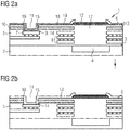
- Figure 2a shows a cross-section of an exemplary embodiment of the optoelectronic device using an optical filter in electrical contact with a contact area.
- Figure 2b shows a cross-section of another exemplary embodiment of the optoelectronic device using an optical filter in electrical contact with a contact area.
- Figure 2d shows a top-view of an embodiment of the optoelectronic device comprising an array of photosensitive structures.
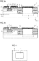
- Figure 3a shows a cross-section of an exemplary embodiment of the optoelectronic device using a spacer structure to connect the contact area to the optical filter.
- Figure 3b shows a cross-section of another exemplary embodiment of the optoelectronic device using a spacer structure to connect the contact area to the optical filter.
- Figure 4 shows a schematic diagram of an electronic device comprising the optoelectronic device.
- FIG. 1a a cross-sectional view of an example for an optoelectronic device 1, which is no embodiment, is shown.
- the feature to be highlighted here is an optical filter 13, which covers a portion of a top surface 6 of a dielectric layer 5 and a portion of an optical element 12.
- the optical filter 13 does not cover a bottom part 14, the sidewalls 15 and the edges 16 of an opening 11 at the top surface 6 of the dielectric layer 5.
- the optical filter 13 is not electrically connected to a fixed electrical potential.
- the optical filter 13 cannot provide EMI-shielding or ESD-protection.
- FIG. 1b a top-view of the example for an optoelectronic device 1 given in Figure 1a is shown.
- the optical filter 13 is spaced from the contact area 9.
- the optical filter 13 does cover the contact area 9.
- Figure 2a shows a cross-sectional view of one exemplary embodiment of the optoelectronic device 1. Elements according to Figure 2a that correspond to elements of the example according to Figure 1a are designated with the same reference numerals.
- the optoelectronic device 1 comprises a substrate 2 and a photosensitive structure 4 at a main surface 3 of the substrate 2.
- the substrate 2 can have a main plane of extension.
- the photosensitive structure 4 can comprise a photodiode, as shown schematically.
- the optoelectronic device 1 can also comprise a plurality of photosensitive structures 4, for example arranged in an array. In an array, each photosensitive structure 4 can be arranged in a similar way as shown in Figure 2a .
- the photosensitive structures 4 in an array can be arranged either next to each other in the cross-sectional plane or in a plane perpendicular to the cross-sectional plane.
- a dielectric layer 5 is arranged on top of the substrate 2 at its main surface 3.
- the dielectric layer 5 has a top surface 6 facing away from the substrate 2.
- the dielectric layer 5 at least one wiring layer 7 is arranged.
- two further wiring layers 8 are arranged in the dielectric layer 5.
- the wiring layer 7 and the further wiring layers 8 may be connected to each other.
- the wiring layer 7 and the further wiring layers 8 may also connect functional parts in the substrate 2, for example the gates of an IC.
- An IC is not shown in Figure 2a .
- a vertical direction z above the photosensitive structure 4 the wiring layers 7 and the further wiring layers 8 are removed, where the vertical direction z extends perpendicular to the main plane of extension of the substrate 2. This means, in a region above the photosensitive structure 4 the dielectric layer 5 is free of the wiring layer 7 and of the further wiring layers 8.
- At least one contact area 9 is formed by a portion of the wiring layer 7. At a side facing away from the substrate 2 the contact area 9 is free of the dielectric layer 5.
- the contact area 9 can have a fixed electrical potential, for example a ground potential.
- the fixed electrical potential can be provided by a further contact area, which is electrically connected to the contact area 9.
- a further contact area is not shown in Figure 2a .
- a passivation layer 10 is arranged in the dielectric layer 5 above the wiring layer 7 and the further wiring layers 8. This means, in vertical direction z the wiring layer 7 and the further wiring layers 8 are arranged between the passivation layer 10 and the substrate 2. A portion of the passivation layer 10 is removed above the photosensitive structure 4. This means, in a region above the photosensitive structure 4 the dielectric layer 5 is free of the passivation layer 10. The passivation layer 10 is also removed in a region above the contact area 9.
- an opening 11 is formed, penetrating the dielectric layer 5 and the passivation layer 10 and extending towards the contact area 9. This means that in a vertical direction z the region above the contact area 9 at a side facing away from the substrate 2 is free of the dielectric layer 5 and the passivation layer 10.
- the depth of the opening 11 from the top surface 6 of the dielectric layer 5 to the contact area 9 may be at least 0.3 micrometer and at most 10 micrometer. Alternatively, the depth of the opening 11 from the top surface 6 of the dielectric layer 5 to the contact area 9 may be at least 0.5 micrometer and at most 3 micrometer.
- optical element 12 is arranged on the top surface 6 of the dielectric layer 5 above the photosensitive structure 4.
- the optical element 12 comprises an interference filter 12.
- the interference filter 12 comprises a stack of alternating layers, for example a stack of alternating oxide and metallic layers.
- An optical filter 13 is arranged on the top surface 6 of the dielectric layer 5.
- the optical filter 13 covers a bottom part 14, the sidewalls 15 and the edges 16 of the opening 11 at the top surface 6 of the dielectric layer 5.
- the optical filter 13 is in direct contact with the contact area 9.
- the optical filter 13 is also in electrical contact with the contact area 9.
- the optical filter 13 also covers the top surface 6 of the dielectric layer 5 in places and a portion of the optical element 12.
- the optical filter 13 is removed on a main part of the optical element 12 above the photosensitive structure 4.
- the aperture 17 extends also in the plane perpendicular to the cross-sectional plane.
- the shape of the aperture 17 can correspond to the shape of the photosensitive structure 4 (see also Figure 2c ).
- the optical filter 13 comprises an electrically conductive layer 18 as well as an anti-reflective coating 19, a black chromium coating 19 or an organic color coating 19 on top of the electrically conductive layer 18.
- the electrically conductive layer 18 is provided for the electrical conductivity as well as for the absorption of unwanted electromagnetic radiation.
- the electrically conductive layer 18 can comprise any material that has favorable electrical, mechanical and optical properties.
- the thickness of the electrically conductive layer 18 has to be in the range that the step coverage from the top surface 6 of the dielectric layer 5 to the contact area 9 is feasible.
- the anti-reflective coating 19 or the black chromium coating 19 or the organic color coating 19 is provided for additional absorption of unwanted electromagnetic radiation and for reducing the reflectivity of the surface of the optoelectronic device 1.
- the overall thickness of the optical filter 13, which means of the electrically conductive layer 18 plus the anti-reflective coating 19 or the black chromium coating 19 or the organic color coating 19, can be at least 0.2 micrometer and at most 10 micrometer. Alternatively, the overall thickness of the optical filter can be at least 0.2 micrometer and at most 5 micrometer.
- Figure 2b shows a cross-sectional view of another exemplary embodiment of the optoelectronic device 1.
- the embodiment according to Figure 2b differs from the embodiment according to Figure 2a in the realization of the optical filter 13.
- the optical filter 13 comprises only one electrically conductive layer with suitable optical properties.
- the optical filter 13 can comprise an electrically conductive black chromium coating or an electrically conductive organic color coating.
- the thickness of the optical filter 13 has to be thick enough to cover the bottom part 14, the sidewalls 15 and the edges 16 of the opening 11 at the top surface 6 of the dielectric layer 5.
- the thickness of the optical filter is in the same range as in the embodiment of Figure 2a .
- Figure 2c shows a top-view of the embodiments according to Figures 2a and 2b .
- a portion of the wiring layer 7 forms a contact area 9 in places, where the opening 11 in the dielectric layer 5 is formed.
- the shape of the contact area 9 is rectangular in top view, but it can have any suitable shape, for example a circular or polygonal shape.
- the wiring layer 7 and the further wiring layers 8 also form an aperture 17 towards the photosensitive structure 4.
- the shape of the aperture 17 in top view corresponds to the shape of the photosensitive structure, in this case a rectangular shape.
- the shape of the photosensitive structure can have any suitable shape, for example a circular or polygonal shape.
- the size of the aperture 17 can be smaller than the size the photosensitive structure 4.
- the passivation layer 10 and the optical filter 13 electromagnetic radiation entering the optoelectronic device 1 can reach the photosensitive structure 4 without being blocked.
- the wiring layer 7 and the further wiring layer 8, which surround the photosensitive structure 4 in a vertical direction z prevent scattered electromagnetic radiation from reaching the photosensitive structure 4. This way, the arrangement of the wiring layer 7 and the further wiring 8 additionally prevents crosstalk between individual photosensitive structures 4.
- the optical filter 13 covers the contact area 9.
- the optical filter 13 is in direct contact with the contact area 9 and electrically connected to the contact area 9.
- the optoelectronic device 1 comprises an array of photosensitive structures 4.
- the array of photosensitive structures 4 comprises three photosensitive structures 4 and extends in a lateral direction y.
- the array of photosensitive structures 4 can also extend in another lateral direction x, which is perpendicular to the lateral direction y.
- the array of photosensitive structures 4 can also extend in both the lateral direction y and the other lateral direction x to form a two-dimensional array.
- the array of photosensitive structures 4 can comprise any number of photosensitive structures 4.
- Figure 3a shows a cross-sectional view of another exemplary embodiment of the optoelectronic device 1. Elements according to Figure 3a that correspond to elements of the embodiment according to Figure 2a are designated with the same reference numerals.
- the embodiment according to Figure 3a differs from the embodiment according to Figure 2a in the fact that a spacer structure 20 covers the bottom part 14, the sidewalls 15 and the edges 16 of the opening 11 at the top surface 6 of the dielectric layer 5.
- the spacer structure 20 is in direct contact with the contact area 9.
- the spacer structure 20 comprises three electrically conductive layers.
- the first electrically conductive layer 21, which is closest to the substrate 2 and in direct contact with the contact area 9, may comprise Al.
- the second conductive layer 22, which is arranged between the first electrically conductive layer 21 and the third electrically conductive layer 23, may comprise Ti.
- the third electrically conductive layer 23, which in a vertical direction z is the topmost layer, may comprise ITO.
- the overall thickness of the spacer structure 20 has to be thick enough to cover the bottom part 14, the sidewalls 15 and the edges 16 of the opening 11 at the top surface 6 of the dielectric layer 5.
- the thickness of the first electrically conductive layer 21 may be 0.3 to 10 micrometer.
- the thickness of the second electrically conductive layer 22 may be 10 nanometer to 1 micrometer.
- the thickness of the third electrically conductive layer 23 may be 10 nanometer to 1 micrometer.
- the thickness of the first electrically conductive layer 21 may be 0.5 to 1.5 micrometer.
- the thickness of the second electrically conductive layer 22 may be 20 to 200 nanometer.
- the thickness of the third electrically conductive layer 23 may be 50 to 200 nanometer.
- the optical filter 13 covers a portion of the spacer structure 20.
- the optical filter 13 is electrically connected to the contact area 9.
- the optical filter 13 comprises an electrically conductive layer 18 as well as an anti-reflective coating 19 or a black chromium coating 19 or an organic color coating 19.
- the electrical and optical properties of the material layers used for the optical filter 13 are the same as described above in the embodiment of Figure 2a .
- the overall thickness of the optical filter 13 can be reduced, since the optical filter 13 does not have to cover the bottom part 14, the sidewalls 15 and the edges 16 of the opening 11 at the top surface 6 of the dielectric layer 5.
- the overall thickness of the optical filter 13 in vertical direction z can be at least 50 nanometer and at most 2 micrometer.
- the overall thickness of the optical filter 13 in vertical direction z can be at least 150 nanometer and at most 800 nanometer.
- an IC 24 is shown within the substrate 2 of the optoelectronic device 1.
- the IC 24 is arranged at the main surface 3 of the substrate 2 in the lateral direction y beside the photosensitive structure 4.
- the IC 24 can also be arranged in the vertical direction z under the photosensitive structure 4 in the substrate 2.
- Figure 3b shows a cross-sectional view of another exemplary embodiment of the optoelectronic device 1. Elements according to Figure 3b that correspond to elements of the embodiment according to Figure 3a are designated with the same reference numerals.
- the embodiment according to Figure 3b differs from the embodiment according to Figure 3a in the realization of the optical filter 13.
- the optical filter 13 comprises only one electrically conductive layer with suitable optical properties.
- the optical filter 13 can comprise an electrically conductive black chromium coating or an electrically conductive organic color coating.
- the thickness of the optical filter 13 can be reduced compared to the embodiment of Figure 2b , since the optical filter 13 does not have to cover the bottom part 14, the sidewalls 15 and the edges 16 of the opening 11 at the top surface 6 of the dielectric layer 5.
- the thickness of the optical filter 13 can be at least 0.1 micrometer and at most 5 micrometer. Alternatively, the thickness of the optical filter 13 can be at least 0.1 micrometer and at most 0.8 micrometer, depending on the used materials.
- Figure 4 shows a schematic diagram of an electronic device 25 comprising the optoelectronic device 1.
- the electronic device 25 can be, for example, a camera system or an electromagnetic radiation sensor.
- the electronic device 25 can be employed for applications in the automotive, the industrial, the medical, the consumer market and the scientific field, for example.
Landscapes
- Physics & Mathematics (AREA)
- Chemical & Material Sciences (AREA)
- Inorganic Chemistry (AREA)
- General Physics & Mathematics (AREA)
- Optics & Photonics (AREA)
- Solid State Image Pick-Up Elements (AREA)
- Light Receiving Elements (AREA)
Abstract
Description
- The present application relates to an optoelectronic device and a method for producing an optoelectronic device.
- Many optoelectronic devices are suitable to detect electromagnetic radiation in a certain wavelength range. In order to prevent leakage of electromagnetic radiation and crosstalk between individual photosensitive structures within an optoelectronic device, frequently a certain area of the senor chip is covered by an optical filter. The optical filter is provided to absorb unwanted electromagnetic radiation at places, where the sensor chip is optically inactive. Besides, the optical filter prevents or reduces the reflectivity of the surface of the sensor chip. This is important, too, since reflected electromagnetic radiation could be scattered back and produce so-called "ghost images" on neighboured photosensitive structures. Therefore, the integration of an optical filter improves an optoelectronic device in terms of its optical properties.
- However, by integrating optoelectronic devices in electronic systems, for example in dense packed camera systems of mobile devices, the optoelectronic device is in close proximity to other electric components. Electric components may produce electromagnetic fields, which possibly cause electromagnetic interference (EMI). This, in turn could cause degradation of individual devices and deterioration of the system performance. Furthermore, each electronic device is prone to damages caused by electrostatic discharge (ESD).
- It is an objective to provide an optoelectronic device with improved optical and electrical properties. It is further an objective to provide a method of producing an optoelectronic device with improved optical and electrical properties.
- This objective is achieved with the independent claims. Further embodiments and variants derive from dependent claims. The definitions as described above also apply to the following description unless otherwise stated.
- In one embodiment the optoelectronic device comprises a substrate, which may comprise a semiconductor material, for example silicon (Si). The substrate can have a main plane of extension. The optoelectronic device may be a complementary metal-oxide-semiconductor (CMOS) device. The optoelectronic device may be arranged in a housing.
- The optoelectronic device further comprises a photosensitive structure in the substrate, which, for example, can be a photodiode or an array of photodiodes. The photosensitive structure can also comprise a phototransistor or an array of phototransistors or any other suitable detection element for detecting electromagnetic radiation. The photosensitive structure can be arranged at a main surface of the substrate. The photosensitive structure can be surrounded by the substrate at side surfaces of the photosensitive structure. This means, the photosensitive structure can be surrounded by the substrate in lateral directions that run parallel to the main plane of extension of the substrate. A top side of the photosensitive structure can be free of the substrate. The photosensitive structure can be configured to detect electromagnetic radiation entering the optoelectronic device at a top side of the optoelectronic device. Wavelengths of the electromagnetic radiation may reach from the ultraviolet (UV) to the mid-infrared (MIR) spectrum.
- The optoelectronic device further comprises a dielectric layer on the main surface of the substrate, the dielectric layer having a top surface facing away from the substrate. The dielectric layer is arranged above the substrate. The dielectric layer can be, for example, a doped or undoped silicon-oxide (SiO2) layer. The dielectric layer can be formed by several deposition steps.
- The optoelectronic device further comprises at least one wiring layer arranged in the dielectric layer in places. The at least one wiring layer comprises a metal, for example aluminum (Al). The at least one wiring layer may electrically connect different functional parts in the substrate, for example the gates of transistors in an integrated circuit (IC). The wiring layer can also electrically contact the photosensitive structure. In a vertical direction above the photosensitive structure the wiring layer is removed, where the vertical direction extends perpendicular to the main plane of extension of the substrate. This means, in a region above the photosensitive structure the dielectric layer is free of the wiring layer. This way, electromagnetic radiation entering the optoelectronic device is not blocked by the at least one wiring layer and can reach the photosensitive structure.
- The optoelectronic device further comprises at least one contact area formed by a portion of the at least one wiring layer. The at least one contact area can be employed for electrically contacting the optoelectronic device. At a side facing away from the substrate the contact area is free of the dielectric layer. The contact area is an area at a surface of the wiring layer. The surface of the wiring layer can be larger than the contact area.
- The optoelectronic device further comprises an opening in the dielectric layer at the top surface, the opening extending towards the contact area. The opening is formed as a trench extending within the dielectric layer in the vertical direction. The opening can have the same extent in the lateral directions as the contact area. Thus, the optoelectronic device can be electrically contacted from the top surface of the dielectric layer. The contact area can exhibit a constant electrical potential, for example a ground potential.
- Besides, the optoelectronic device comprises an optical element arranged on the top surface of the dielectric layer above the photosensitive structure. The optical element is arranged above the photosensitive structure in the vertical direction. The optical element may be suitable to direct electromagnetic radiation of a certain wavelength or in a certain range of wavelengths towards the photosensitive structure.
- Furthermore, the optoelectronic device comprises an optical filter arranged on the top surface of the dielectric layer. The optical filter is electrically conductive and in electrical contact with the contact area. It also covers a portion of the optical element. In this way, the optical filter provides an aperture towards the photosensitive structure. The optical filter can show a low angular dependency for incoming electromagnetic radiation. The optical filter can have a reflectivity of at most 0.2 in a wavelength range of 300 nm to 1200 nm. Preferably, the optical filter has a reflectivity of at most 0.03 in a wavelength range of 300 nm to 1200 nm. The optical filter absorbs unwanted electromagnetic radiation and prevents or reduces reflection on the surface of the optoelectronic device because of its optical properties. Besides, because of its electrical properties, it provides a shielding from EMI and a protection from ESD.
- The optical filter improves the optical properties of the optoelectronic device. On the one hand, this is because the optical filter prevents or reduces reflection of electromagnetic radiation on the surface of the optoelectronic device. In case of no optical filter reflected electromagnetic radiation could be reflected back in an uncontrolled way, for example by the housing of the optoelectronic device.
- On the other hand, the optical filter also absorbs electromagnetic radiation in places where the optoelectronic device is optically inactive. This means that the electromagnetic radiation is blocked from entering the optoelectronic device in places where no photosensitive structure lies underneath in the substrate. Therefore, electromagnetic radiation cannot enter the optoelectronic device at places, where the electromagnetic radiation would propagate and be reflected in an uncontrolled way.
- This way, leakage of electromagnetic radiation is prevented. Besides, optical crosstalk between individual photosensitive structures is prevented. This in turn improves the signal-to-noise ratio and thus the accuracy of the optoelectronic device.
- The optical filter also improves the electrical properties of the optoelectronic device. This is because the optical filter is electrically connected to a contact area, which can have a fixed electrical potential, for example a ground potential. Thus, the optoelectronic device is protected from ESD, since electrical charges can discharge and thus do not cause damage to electronic components of the device.
- Besides, because of being electrically conductive the optical filter shields the optoelectronic device from electromagnetic fields and isolates it from its surrounding environment. This way, the optical filter provides protection against interfering signals, for example radio frequency (RF) signals.
- In an embodiment the optical filter covers a bottom part, the sidewalls and the edges of the opening at the top surface of the dielectric layer. The bottom part of the opening is the part of the opening facing the contact area. The sidewalls of the opening extend perpendicular or transverse to the main plane of extension of the substrate. The edges of the opening are arranged at the top surface of the dielectric layer. The edges delimit the opening. The optical filter can be in direct contact with the contact area. This way, the optical filter is electrically connected to the contact area. By electrically connecting the optical filter to a fixed constant potential via the contact area, the optical filter provides ESD-protection to the optoelectronic device. It also provides EMI-shielding to the optoelectronic device.
- In another embodiment the optoelectronic device further comprises a spacer structure covering the bottom part, the sidewalls and the edges of the opening at the top surface of the dielectric layer. The spacer structure is in direct contact with the contact area and with the optical filter. This way, the spacer structure electrically connects the contact area to the optical filter. When using a spacer structure the optical filter can be thin in the vertical direction, since it does not have to cover the edges of the opening of the dielectric layer. Thin layers have less intrinsic stress than thick layers and can be patterned more easily. Thus, using thin layers for realizing the optical filter can be advantageous, if there are limitations regarding mechanical stress or special requirements for the patterning of the optical filter.
- In an embodiment the spacer structure comprises a stack of at least two electrically conductive layers.
For example, the spacer structure may comprise a first electrically conductive layer, a second electrically conductive layer and a third electrically conductive layer. The first electrically conductive layer can comprise Al. The second electrically conductive layer can comprise titanium (Ti). The third electrically conductive layer can comprise indium tin oxide (ITO). However, the spacer structure is not limited to comprise those materials and may comprise any other suitable materials. The advantage of a layer stack comprising Al, Ti and ITO is that Al has a good electrical conductivity and is compatible to CMOS processing. The Tilayer is provided as a buffer layer and to provide good adhesion of the ITO-layer. The ITO-layer prevents corroding of the Al-layer. The electrically conductive layers are arranged on top of each over. The second electrically conductive layer covers the first electrically conductive layer. The third electrically conductive layer covers the second electrically conductive layer. The second conductive layer can be arranged between the first conductive layer and the third conductive layer in vertical direction. The first conductive layer can be arranged closer to the substrate than the second and the third conductive layer. - In an embodiment the optical filter comprises an electrically conductive layer. The electrically conductive layer may comprise, for example, Al. However, the electrically conductive layer of the optical filter is not limited to be an Al-layer and may comprise any other suitable electrically conductive material. The optical filter further comprises an anti-reflective coating on top of the electrically conductive layer. This means, the anti-reflective coating is arranged at the side of the electrically conductive layer that faces away from the substrate. The anti-reflective coating comprises, for example, a stack of alternating dielectric and metallic layers. The anti-reflective coating may also comprise a stack of alternating dielectric layers. The anti-reflective coating may also comprise a stack of alternating nitride and metallic layers. The amount as well as the thickness of the alternating layers can vary depending on the application.
- The electrically conductive layer of the optical filter is provided for the electrical conductivity of the optical filter as well as for the absorption of unwanted electromagnetic radiation. The anti-reflective coating of the optical filter is provided for the reduction of the reflectivity of the surface of the optoelectronic device facing the entering electromagnetic radiation. The anti-reflective coating shows a low angular dependency for incoming electromagnetic radiation. For example, the reflectivity of the anti-reflective coating is less than 0.2 in a wavelength range of 300 nm to 1200 nm. Preferably, the reflectivity of the anti-reflective coating can have a reflectivity of at most 0.03 in a wavelength range of 300 to 1200 nanometer.
- In another embodiment the optical filter comprises an electrically conductive black chromium coating. The black chromium coating is a layer arranged at the top side of the optoelectronic device. The black chromium coating comprises chromium. For example, the reflectivity of the black chromium coating is typically less than 5 % in a wavelength range of 300 to 1200 nanometer.
- The electrically conductive black chromium coating is provided for the electrical conductivity of the optical filter and for the absorption of unwanted electromagnetic radiation as well as for the reduction of reflectivity of the surface of the optoelectronic device facing the entering electromagnetic radiation.
- In another embodiment the optical filter comprises an electrically conductive layer and a black chromium layer on top of the electrically conductive layer. The electrically conductive layer may comprise, for example, metallic chrome (Cr) or any other suitable material like Al, Ti or silver (Ag) .
- The electrically conductive layer is provided for the electrical conductivity of the optical filter and for the absorption of unwanted electromagnetic radiation. The black chromium layer is provided for further absorption of electromagnetic radiation as well as for reduction of reflectivity of the surface of the optoelectronic device facing the entering electromagnetic radiation.
- In another embodiment the optical filter comprises an electrically conductive organic color coating. The organic color coating is a layer arranged at the top side of the optoelectronic device. The organic color coating comprises an organic material, for example a resist. For example, the reflectivity of the organic color coating is less than 0.2 in a wavelength range of 300 to 1200 nanometer. Preferably, the reflectivity of the organic color coating can have a reflectivity of at most 0.03 in a wavelength range of 300 to 1200 nanometer. The electrical conductivity of the organic color coating may be realized by the addition of carbon nanotubes or carbon black or by the addition of electrically conductive polymers like PEDOT:PSS.
- The electrically conductive organic color coating is provided for the electrical conductivity of the optical filter and for the absorption of unwanted electromagnetic radiation as well as for the reduction of reflectivity of the surface of the optoelectronic device facing the entering electromagnetic radiation.
- In a further embodiment the optical filter comprises an electrically conductive layer, for example a layer comprising Al, and an organic color coating on top of the electrically conductive layer.
- The electrically conductive layer is provided for the electrical conductivity of the optical filter and for the absorption of unwanted electromagnetic radiation. The organic color coating is provided for further absorption of electromagnetic radiation as well as for reduction of reflectivity of the surface of the optoelectronic device facing the entering electromagnetic radiation.
- In a further embodiment the optoelectronic device comprises a passivation layer arranged in the dielectric layer in places. The passivation layer may comprise, for example, silicon-nitride (Si3N4). The passivation layer is arranged above the at least one wiring layer. This means, in vertical direction the wiring layer is arranged between the passivation layer and the substrate. In vertical direction above the photosensitive structure the passivation layer is removed. This means, in a region above the photosensitive structure the dielectric layer is free of the passivation layer. This way, electromagnetic radiation entering the optoelectronic device is not blocked by the passivation layer and can reach the photosensitive structure. Besides, unwanted interference of the electromagnetic radiation on the passivation layer is prevented. The passivation layer is also removed in the region above the contact area by forming the opening in the dielectric layer as described above.
- By using a passivation layer the optoelectronic device becomes more resistant to the environment. For example, the optoelectronic device becomes more resistant to scratches or humidity.
- In a further embodiment the optoelectronic device comprises an IC in the substrate. The IC can be arranged in beside the photosensitive structure in the substrate. This means that in lateral directions, that run parallel to the main plane of extension of the substrate, the IC can be adjacent to the photosensitive structure. The IC also can be arranged in the vertical direction under the photosensitive structure in the substrate.
- By employing an IC, the photosensitive structure can be controlled. Electrical signals coming from the photosensitive structure can be processed efficiently. Besides, the optoelectronic device can communicate with other electrical components via the IC.
- In a further embodiment the optical element of the optoelectronic device is an interference filter. The interference filter can comprise a stack of alternating dielectric and metallic layers. The interference filter can be realized as, for example, a longpass filter or a bandpass filter.
- The purpose of using an interference filter is to transmit only a certain wavelength or a certain range of wavelengths to the photosensitive structure. This way, the signal-to-noise ratio of the optoelectronic device can be improved.
- In a further embodiment the photosensitive structure is a single photodiode or an array of photodiodes. In case of an array of photodiodes, the array can have a rectangular shape. In the array, the photodiodes can be arranged at lattice points of a lattice. The lattice can be linear or two-dimensional. The photodiodes in an array can be arranged beside each other. This means that in lateral directions the photodiodes can be adjacent to each other. Each photodiode in an array of photodiodes can be arranged within the optoelectronic device as described above. This means that the region in the dielectric layer above each photodiodes is free of a wiring layer and free of a passivation layer and there is an optical element on the top surface of the dielectric layer above each photodiode and the optical filter forms an aperture towards each photodiode. By using an array of photodiodes applications like imaging are possible.
- In a further embodiment the optoelectronic device is incorporated in an electronic device. The electronic device can be, for example, a camera system. The camera system can be used for imaging a scene in a desired wavelength range. For example, the camera system can be used for imaging in the visible light spectrum. The camera system can advantageously be arranged in close proximity to other electronic components, since due to the EMI-shielding properties of the optical filter the camera system is more resistant to issues relating to electromagnetic interference. The optoelectronic device is not limited to be incorporated in a camera system, but it can be incorporated in any electronic device such as an electromagnetic radiation sensor device.
- Furthermore, a method of producing an optoelectronic device is provided. All features disclosed for the optoelectronic device are also disclosed for the method for producing the optoelectronic device and vice-versa.
- The method of producing an optoelectronic device comprises providing a substrate and forming a photosensitive structure in the substrate. In case of the photosensitive structure being a photodiode, the photodiode can be realized by ion-implantation. A dielectric layer is deposited on top of the substrate, the dielectric layer having a top surface facing away from the substrate. The deposition of the dielectric layer can comprise several deposition steps. The deposition can be realized by chemical vapor deposition (CVD), for example. The dielectric layer can be in direct contact with the substrate.
- At least one wiring layer is deposited and arranged in places within the dielectric layer. This means a part of the dielectric layer is deposited on the substrate, and the wiring layer is deposited on the dielectric layer. Afterwards, another deposition step for the deposition of the dielectric layer follows so that the wiring layer is arranged in places within the dielectric layer. The wiring layer can be deposited by a sputter process and patterned by an etching procedure.
- The wiring layer forms a contact area in places. This means, a part of the wiring layer, namely the contact area, is configured to be electrically contacted. The wiring layer can be removed above the photosensitive structure.
- An opening is formed at the top surface of the dielectric layer, the opening extending towards the contact area. The opening is formed by removing the material arranged above the contact area. The opening can be formed by etching.
- An optical element is deposited on the dielectric layer, the optical element being arranged in a vertical direction above the photosensitive structure. The optical element can be deposited, for example, by CVD, atomic layer deposition (ALD) or physical vapor deposition (PVD). The patterning of the optical element can be done by etching.
- An optical filter is deposited. The optical filter can be deposited in places on the top surface of the dielectric layer and on a portion of the optical element. Depending on the used materials for the optical filter the deposition technique can include CVD, ALD, PVD, spin coating or sputter processes. The patterning of the optical filter can be done, for example, by etching.
- In one embodiment of the method of producing an optoelectronic device the optical filter is arranged on the top surface of the dielectric layer in places, on a portion of the optical element and in the opening of the dielectric layer, the optical filter covering a bottom part, the sidewalls and the edges of the opening at the top surface of the dielectric layer. This way, the optical filter is electrically connected to the contact area. By electrically connecting the optical filter to a fixed constant potential via the contact area, the optical filter provides ESD-protection to the optoelectronic device.
- In another embodiment of the method of producing an optoelectronic device a spacer structure is deposited into the opening of the dielectric layer and onto the contact area before the deposition of the optical filter, the spacer structure covering a bottom part, the sidewalls and the edges of the opening at the top surface of the dielectric layer. The spacer structure is in direct contact with the contact area. The deposition technique for the spacer structure depends on the materials used. It can, for example, include sputter techniques. The used material layers for the spacer structure can be patterned by etching. The optical filter is deposited after the deposition of the spacer structure. When using a spacer structure the optical filter can be thin in the vertical direction, since it does not have to cover the edges of the opening in the dielectric layer.
- In another embodiment of the method of producing an optoelectronic device the optical filter is arranged on the top surface of the dielectric layer in places, on a portion of the optical element and on a portion of the spacer structure. This way, the optical filter is electrically connected to the contact area. By electrically connecting the optical filter to a fixed constant potential via the contact area, the optical filter provides ESD-protection to the optoelectronic device.
- The following description of figures may further illustrate and explain exemplary embodiments. Components that are functionally identical or have an identical effect are denoted by identical references. Identical or effectively identical components might be described only with respect to the figures where they occur first. Their description is not necessarily repeated in successive figures.
-
Figure 1a shows a cross-section of an example for an optoelectronic device using an optical filter. - In
Figure 1b the top-view of an example for an optoelectronic device using an optical filter is shown. -
Figure 2a shows a cross-section of an exemplary embodiment of the optoelectronic device using an optical filter in electrical contact with a contact area. -
Figure 2b shows a cross-section of another exemplary embodiment of the optoelectronic device using an optical filter in electrical contact with a contact area. - In
Figure 2c the top-view of an embodiment of the optoelectronic device using an optical filter in electrical contact with a contact area is shown. -
Figure 2d shows a top-view of an embodiment of the optoelectronic device comprising an array of photosensitive structures. -
Figure 3a shows a cross-section of an exemplary embodiment of the optoelectronic device using a spacer structure to connect the contact area to the optical filter. -
Figure 3b shows a cross-section of another exemplary embodiment of the optoelectronic device using a spacer structure to connect the contact area to the optical filter. -
Figure 4 shows a schematic diagram of an electronic device comprising the optoelectronic device. - In
Figure 1a a cross-sectional view of an example for anoptoelectronic device 1, which is no embodiment, is shown. The feature to be highlighted here is anoptical filter 13, which covers a portion of atop surface 6 of adielectric layer 5 and a portion of anoptical element 12. Theoptical filter 13 does not cover abottom part 14, thesidewalls 15 and theedges 16 of anopening 11 at thetop surface 6 of thedielectric layer 5. Thus, theoptical filter 13 is not electrically connected to a fixed electrical potential. Thus, theoptical filter 13 cannot provide EMI-shielding or ESD-protection. - With
Figure 1b a top-view of the example for anoptoelectronic device 1 given inFigure 1a is shown. Theoptical filter 13 is spaced from thecontact area 9. Thus, it becomes clear that theoptical filter 13 does cover thecontact area 9. -
Figure 2a shows a cross-sectional view of one exemplary embodiment of theoptoelectronic device 1. Elements according toFigure 2a that correspond to elements of the example according toFigure 1a are designated with the same reference numerals. - The
optoelectronic device 1 according toFigure 2a comprises asubstrate 2 and aphotosensitive structure 4 at amain surface 3 of thesubstrate 2. Thesubstrate 2 can have a main plane of extension. Thephotosensitive structure 4 can comprise a photodiode, as shown schematically. Theoptoelectronic device 1 can also comprise a plurality ofphotosensitive structures 4, for example arranged in an array. In an array, eachphotosensitive structure 4 can be arranged in a similar way as shown inFigure 2a . Thephotosensitive structures 4 in an array can be arranged either next to each other in the cross-sectional plane or in a plane perpendicular to the cross-sectional plane. - A
dielectric layer 5 is arranged on top of thesubstrate 2 at itsmain surface 3. Thedielectric layer 5 has atop surface 6 facing away from thesubstrate 2. - In the
dielectric layer 5 at least one wiring layer 7 is arranged. In the embodiment shown inFigure 2a two further wiring layers 8 are arranged in thedielectric layer 5. The wiring layer 7 and the further wiring layers 8 may be connected to each other. The wiring layer 7 and the further wiring layers 8 may also connect functional parts in thesubstrate 2, for example the gates of an IC. An IC is not shown inFigure 2a . In a vertical direction z above thephotosensitive structure 4 the wiring layers 7 and the further wiring layers 8 are removed, where the vertical direction z extends perpendicular to the main plane of extension of thesubstrate 2. This means, in a region above thephotosensitive structure 4 thedielectric layer 5 is free of the wiring layer 7 and of the further wiring layers 8. - At least one
contact area 9 is formed by a portion of the wiring layer 7. At a side facing away from thesubstrate 2 thecontact area 9 is free of thedielectric layer 5. Thecontact area 9 can have a fixed electrical potential, for example a ground potential. The fixed electrical potential can be provided by a further contact area, which is electrically connected to thecontact area 9. A further contact area is not shown inFigure 2a . - A
passivation layer 10 is arranged in thedielectric layer 5 above the wiring layer 7 and the further wiring layers 8. This means, in vertical direction z the wiring layer 7 and the further wiring layers 8 are arranged between thepassivation layer 10 and thesubstrate 2. A portion of thepassivation layer 10 is removed above thephotosensitive structure 4. This means, in a region above thephotosensitive structure 4 thedielectric layer 5 is free of thepassivation layer 10. Thepassivation layer 10 is also removed in a region above thecontact area 9. - At the
top surface 6 of thedielectric layer 5 anopening 11 is formed, penetrating thedielectric layer 5 and thepassivation layer 10 and extending towards thecontact area 9. This means that in a vertical direction z the region above thecontact area 9 at a side facing away from thesubstrate 2 is free of thedielectric layer 5 and thepassivation layer 10. The depth of the opening 11 from thetop surface 6 of thedielectric layer 5 to thecontact area 9 may be at least 0.3 micrometer and at most 10 micrometer. Alternatively, the depth of the opening 11 from thetop surface 6 of thedielectric layer 5 to thecontact area 9 may be at least 0.5 micrometer and at most 3 micrometer. - An
optical element 12 is arranged on thetop surface 6 of thedielectric layer 5 above thephotosensitive structure 4. In the embodiment shown inFigure 2a theoptical element 12 comprises aninterference filter 12. Theinterference filter 12 comprises a stack of alternating layers, for example a stack of alternating oxide and metallic layers. - An
optical filter 13 is arranged on thetop surface 6 of thedielectric layer 5. Theoptical filter 13 covers abottom part 14, thesidewalls 15 and theedges 16 of theopening 11 at thetop surface 6 of thedielectric layer 5. Thus, theoptical filter 13 is in direct contact with thecontact area 9. Thus, theoptical filter 13 is also in electrical contact with thecontact area 9. Theoptical filter 13 also covers thetop surface 6 of thedielectric layer 5 in places and a portion of theoptical element 12. Theoptical filter 13 is removed on a main part of theoptical element 12 above thephotosensitive structure 4. - The removal of the
optical filter 13 as well as of thepassivation layer 10, the wiring layer 7 and the further wiring layer 8 forms anaperture 17 towards thephotosensitive structure 4. This means that in a vertical direction z above thephotosensitive structure 4 theoptoelectronic device 1 is free of these layers. Theaperture 17 extends also in the plane perpendicular to the cross-sectional plane. The shape of theaperture 17 can correspond to the shape of the photosensitive structure 4 (see alsoFigure 2c ). - In the embodiment shown in
Figure 2a theoptical filter 13 comprises an electricallyconductive layer 18 as well as ananti-reflective coating 19, ablack chromium coating 19 or anorganic color coating 19 on top of the electricallyconductive layer 18. The electricallyconductive layer 18 is provided for the electrical conductivity as well as for the absorption of unwanted electromagnetic radiation. The electricallyconductive layer 18 can comprise any material that has favorable electrical, mechanical and optical properties. The thickness of the electricallyconductive layer 18 has to be in the range that the step coverage from thetop surface 6 of thedielectric layer 5 to thecontact area 9 is feasible. Theanti-reflective coating 19 or theblack chromium coating 19 or theorganic color coating 19 is provided for additional absorption of unwanted electromagnetic radiation and for reducing the reflectivity of the surface of theoptoelectronic device 1. The overall thickness of theoptical filter 13, which means of the electricallyconductive layer 18 plus theanti-reflective coating 19 or theblack chromium coating 19 or theorganic color coating 19, can be at least 0.2 micrometer and at most 10 micrometer. Alternatively, the overall thickness of the optical filter can be at least 0.2 micrometer and at most 5 micrometer. -
Figure 2b shows a cross-sectional view of another exemplary embodiment of theoptoelectronic device 1. - The embodiment according to
Figure 2b differs from the embodiment according toFigure 2a in the realization of theoptical filter 13. In this embodiment theoptical filter 13 comprises only one electrically conductive layer with suitable optical properties. Theoptical filter 13 can comprise an electrically conductive black chromium coating or an electrically conductive organic color coating. In both cases the thickness of theoptical filter 13 has to be thick enough to cover thebottom part 14, thesidewalls 15 and theedges 16 of theopening 11 at thetop surface 6 of thedielectric layer 5. Thus, the thickness of the optical filter is in the same range as in the embodiment ofFigure 2a .Figure 2c shows a top-view of the embodiments according toFigures 2a and 2b . - A portion of the wiring layer 7 forms a
contact area 9 in places, where theopening 11 in thedielectric layer 5 is formed. In this embodiment the shape of thecontact area 9 is rectangular in top view, but it can have any suitable shape, for example a circular or polygonal shape. - The wiring layer 7 and the further wiring layers 8 also form an
aperture 17 towards thephotosensitive structure 4. The shape of theaperture 17 in top view corresponds to the shape of the photosensitive structure, in this case a rectangular shape. However, the shape of the photosensitive structure can have any suitable shape, for example a circular or polygonal shape. The size of theaperture 17 can be smaller than the size thephotosensitive structure 4. - On the one hand, due to the
aperture 17 in the wiring layers 7 and 8, thepassivation layer 10 and theoptical filter 13 electromagnetic radiation entering theoptoelectronic device 1 can reach thephotosensitive structure 4 without being blocked. On the other hand, the wiring layer 7 and the further wiring layer 8, which surround thephotosensitive structure 4 in a vertical direction z, prevent scattered electromagnetic radiation from reaching thephotosensitive structure 4. This way, the arrangement of the wiring layer 7 and the further wiring 8 additionally prevents crosstalk between individualphotosensitive structures 4. - The
optical filter 13 covers thecontact area 9. Thus, theoptical filter 13 is in direct contact with thecontact area 9 and electrically connected to thecontact area 9. - With
Figure 2d a top-view of another embodiment is shown, wherein theoptoelectronic device 1 comprises an array ofphotosensitive structures 4. In this embodiment, the array ofphotosensitive structures 4 comprises threephotosensitive structures 4 and extends in a lateral direction y. The array ofphotosensitive structures 4 can also extend in another lateral direction x, which is perpendicular to the lateral direction y. The array ofphotosensitive structures 4 can also extend in both the lateral direction y and the other lateral direction x to form a two-dimensional array. In each lateral direction the array ofphotosensitive structures 4 can comprise any number ofphotosensitive structures 4. -
Figure 3a shows a cross-sectional view of another exemplary embodiment of theoptoelectronic device 1. Elements according toFigure 3a that correspond to elements of the embodiment according toFigure 2a are designated with the same reference numerals. - The embodiment according to
Figure 3a differs from the embodiment according toFigure 2a in the fact that aspacer structure 20 covers thebottom part 14, thesidewalls 15 and theedges 16 of theopening 11 at thetop surface 6 of thedielectric layer 5. Thus, thespacer structure 20 is in direct contact with thecontact area 9. Thespacer structure 20 comprises three electrically conductive layers. The first electricallyconductive layer 21, which is closest to thesubstrate 2 and in direct contact with thecontact area 9, may comprise Al. The secondconductive layer 22, which is arranged between the first electricallyconductive layer 21 and the third electricallyconductive layer 23, may comprise Ti. The third electricallyconductive layer 23, which in a vertical direction z is the topmost layer, may comprise ITO. The overall thickness of thespacer structure 20 has to be thick enough to cover thebottom part 14, thesidewalls 15 and theedges 16 of theopening 11 at thetop surface 6 of thedielectric layer 5. The thickness of the first electricallyconductive layer 21 may be 0.3 to 10 micrometer. The thickness of the second electricallyconductive layer 22 may be 10 nanometer to 1 micrometer. The thickness of the third electricallyconductive layer 23 may be 10 nanometer to 1 micrometer. Alternatively, the thickness of the first electricallyconductive layer 21 may be 0.5 to 1.5 micrometer. Alternatively, the thickness of the second electricallyconductive layer 22 may be 20 to 200 nanometer. Alternatively, the thickness of the third electricallyconductive layer 23 may be 50 to 200 nanometer. - The
optical filter 13 covers a portion of thespacer structure 20. Thus, theoptical filter 13 is electrically connected to thecontact area 9. In the embodiment according toFigure 3a theoptical filter 13 comprises an electricallyconductive layer 18 as well as ananti-reflective coating 19 or ablack chromium coating 19 or anorganic color coating 19. The electrical and optical properties of the material layers used for theoptical filter 13 are the same as described above in the embodiment ofFigure 2a . But the overall thickness of theoptical filter 13 can be reduced, since theoptical filter 13 does not have to cover thebottom part 14, thesidewalls 15 and theedges 16 of theopening 11 at thetop surface 6 of thedielectric layer 5. The overall thickness of theoptical filter 13 in vertical direction z can be at least 50 nanometer and at most 2 micrometer. Alternatively, the overall thickness of theoptical filter 13 in vertical direction z can be at least 150 nanometer and at most 800 nanometer. - Besides, with
Figure 3a anIC 24 is shown within thesubstrate 2 of theoptoelectronic device 1. In this embodiment theIC 24 is arranged at themain surface 3 of thesubstrate 2 in the lateral direction y beside thephotosensitive structure 4. TheIC 24 can also be arranged in the vertical direction z under thephotosensitive structure 4 in thesubstrate 2. -
Figure 3b shows a cross-sectional view of another exemplary embodiment of theoptoelectronic device 1. Elements according toFigure 3b that correspond to elements of the embodiment according toFigure 3a are designated with the same reference numerals. - The embodiment according to
Figure 3b differs from the embodiment according toFigure 3a in the realization of theoptical filter 13. In this embodiment theoptical filter 13 comprises only one electrically conductive layer with suitable optical properties. Theoptical filter 13 can comprise an electrically conductive black chromium coating or an electrically conductive organic color coating. The thickness of theoptical filter 13 can be reduced compared to the embodiment ofFigure 2b , since theoptical filter 13 does not have to cover thebottom part 14, thesidewalls 15 and theedges 16 of theopening 11 at thetop surface 6 of thedielectric layer 5. The thickness of theoptical filter 13 can be at least 0.1 micrometer and at most 5 micrometer. Alternatively, the thickness of theoptical filter 13 can be at least 0.1 micrometer and at most 0.8 micrometer, depending on the used materials. -
Figure 4 shows a schematic diagram of anelectronic device 25 comprising theoptoelectronic device 1. Theelectronic device 25 can be, for example, a camera system or an electromagnetic radiation sensor. Theelectronic device 25 can be employed for applications in the automotive, the industrial, the medical, the consumer market and the scientific field, for example. -
- 1
- optoelectronic device
- 2
- substrate
- 3
- main surface of the substrate
- 4
- photosensitive structure
- 5
- dielectric layer
- 6
- top surface of the dielectric layer
- 7
- wiring layer
- 8
- further wiring layer
- 9
- contact area
- 10
- passivation layer
- 11
- opening
- 12
- optical element
- 13
- optical filter
- 14
- bottom part of opening
- 15
- sidewalls of opening
- 16
- edges of opening
- 17
- aperture
- 18
- electrically conductive layer of optical filter
- 19
- anti-reflective coating or black chromium coating or organic color coating
- 20
- spacer structure
- 21
- first electrically conductive layer of spacer structure
- 22
- second electrically conductive layer of spacer structure
- 23
- third electrically conductive layer of spacer structure
- 24
- integrated circuit (IC)
- 25
- electronic device
- x,y
- lateral directions
- z
- vertical direction
Claims (15)
- Optoelectronic device (1), comprising:- a substrate (2) with a photosensitive structure (4),- a dielectric layer (5) on a main surface (3) of the substrate (2), the dielectric layer (5) having a top surface (6) facing away from the substrate (2),- at least one wiring layer (7) arranged in the dielectric layer (5) in places,- at least one contact area (9) formed by a portion of the at least one wiring layer (7),- an opening (11) in the dielectric layer (5) at the top surface (6), the opening (11) extending towards the contact area (9),- an optical element (12) arranged on the top surface (6) of the dielectric layer (5) above the photosensitive structure (4), and- an optical filter (13) arranged on the top surface (6) of the dielectric layer (5), the optical filter (13) being electrically conductive, covering a portion of the optical element (12) and being in electrical contact with the contact area (9).
- Optoelectronic device (1) according to claim 1, wherein the optical filter (13) covers a bottom part (14), the sidewalls (15) and the edges (16) of the opening (11) at the top surface (6) of the dielectric layer (5) and electrically contacts the contact area (9).
- Optoelectronic device (1) according to claim 1, comprising:
a spacer structure (20), the spacer structure (20) covering a bottom part (14), the sidewalls (15) and the edges (16) of the opening (11) at the top surface (6) of the dielectric layer (5) and electrically connecting the contact area (9) to the optical filter (13). - Optoelectronic device (1) according to claim 3, wherein the spacer structure (20) comprises a stack of at least two electrically conductive layers (21, 22, 23).
- Optoelectronic device (1) according to one of claims 1 to 4, wherein
the optical filter (13) comprises an electrically conductive layer (18). - Optoelectronic device (1) according to one of claims 1 to 5, wherein
the optical filter (13) comprises an anti-reflective coating (19), an organic color coating (19) or a black chromium coating (19). - Optoelectronic device (1) according to one of claims 1 to 6, comprising:
a passivation layer (10) arranged in places in the dielectric layer (5) above the at least one wiring layer (7). - Optoelectronic device (1) according to one of claims 1 to 7, comprising:
an integrated circuit (24) in the substrate (2). - Optoelectronic device (1) according to one of claims 1 to 8, wherein
the optical element (12) is an interference filter. - Optoelectronic device (1) according to one of claims 1 to 9, wherein
the photosensitive structure (4) is a single photodiode or an array of photodiodes. - Electronic device (25) comprising an optoelectronic device (1) according to one of claims 1 to 10, wherein in particular the electronic device (25) is a camera system or an electromagnetic radiation sensor.
- Method of producing an optoelectronic device (1), comprising:- providing a substrate (2) and forming a photosensitive structure (4) in the substrate (2),- deposition of a dielectric layer (5) on top of the substrate (2), the dielectric layer (5) having a top surface (6) facing away from the substrate (2),- deposition of at least one wiring layer (7), the at least one wiring layer (7) being arranged within the dielectric layer (5) in places, forming a contact area (9) in places,- forming an opening (11) at the top surface (6) of the dielectric layer (5), the opening (11) extending towards the contact area (9),- deposition of an optical element (12) on the dielectric layer (5), the optical element (12) being arranged above the photosensitive structure (4) in the substrate (2), and- deposition of an optical filter (13).
- Method according to claim 12, wherein
the optical filter (13) is arranged on the top surface (6) of the dielectric layer (5) in places, on a portion of the optical element (12) and in the opening (11) of the dielectric layer (5), the optical filter (13) covering a bottom part (14), the sidewalls (15) and the edges (16) of the opening (11) at the top surface (6) of the dielectric layer (5). - Method according to claim 12, comprising:
deposition of a spacer structure (20) into the opening (11) of the dielectric layer (5) and onto the contact area (9) before the deposition of the optical filter (13), the spacer structure (20) covering a bottom part (14), the sidewalls (15) and the edges (16) of the opening (11) at the top surface (6) of the dielectric layer (5). - Method according to claim 14, wherein
the optical filter (13) is arranged on the top surface (6) of the dielectric layer (5) in places, on a portion of the optical element (12) and on a portion of the spacer structure (20) .
Priority Applications (5)
| Application Number | Priority Date | Filing Date | Title |
|---|---|---|---|
| EP19191268.2A EP3780120B1 (en) | 2019-08-12 | 2019-08-12 | Optoelectronic device and method of producing an optoelectronic device |
| PCT/EP2020/070541 WO2021028164A1 (en) | 2019-08-12 | 2020-07-21 | Optoelectronic device and method of producing an optoelectronic device |
| US17/634,665 US12218162B2 (en) | 2019-08-12 | 2020-07-21 | Optoelectronic device and method of producing an optoelectronic device |
| CN202080057069.1A CN114521292B (en) | 2019-08-12 | 2020-07-21 | Optoelectronic device and method for manufacturing the same |
| JP2022503576A JP7329128B2 (en) | 2019-08-12 | 2020-07-21 | Optoelectronic device and method of manufacturing an optoelectronic device |
Applications Claiming Priority (1)
| Application Number | Priority Date | Filing Date | Title |
|---|---|---|---|
| EP19191268.2A EP3780120B1 (en) | 2019-08-12 | 2019-08-12 | Optoelectronic device and method of producing an optoelectronic device |
Publications (2)
| Publication Number | Publication Date |
|---|---|
| EP3780120A1 true EP3780120A1 (en) | 2021-02-17 |
| EP3780120B1 EP3780120B1 (en) | 2022-11-09 |
Family
ID=67620262
Family Applications (1)
| Application Number | Title | Priority Date | Filing Date |
|---|---|---|---|
| EP19191268.2A Active EP3780120B1 (en) | 2019-08-12 | 2019-08-12 | Optoelectronic device and method of producing an optoelectronic device |
Country Status (5)
| Country | Link |
|---|---|
| US (1) | US12218162B2 (en) |
| EP (1) | EP3780120B1 (en) |
| JP (1) | JP7329128B2 (en) |
| CN (1) | CN114521292B (en) |
| WO (1) | WO2021028164A1 (en) |
Citations (4)
| Publication number | Priority date | Publication date | Assignee | Title |
|---|---|---|---|---|
| US20060115230A1 (en) * | 2002-12-13 | 2006-06-01 | Tetsuya Komoguchi | Solid-state imaging device and production method therefor |
| US20090162967A1 (en) * | 2007-12-20 | 2009-06-25 | Visera Technologies Company Limited | Method for forming light-transmitting regions |
| US20140264298A1 (en) * | 2013-03-15 | 2014-09-18 | Samsung Electronics Co., Ltd. | Image sensor and method of forming the same |
| US20190229143A1 (en) * | 2018-01-22 | 2019-07-25 | Semiconductor Components Industries, Llc | Apparatus and method related to sensor die esd protection |
Family Cites Families (17)
| Publication number | Priority date | Publication date | Assignee | Title |
|---|---|---|---|---|
| US5091244A (en) | 1990-08-10 | 1992-02-25 | Viratec Thin Films, Inc. | Electrically-conductive, light-attenuating antireflection coating |
| JPH05275731A (en) * | 1992-03-25 | 1993-10-22 | Sharp Corp | Photodiode |
| JPH06326282A (en) * | 1993-05-11 | 1994-11-25 | Fuji Electric Co Ltd | Light-shielding and connection structure of integrated circuit device |
| JP3503410B2 (en) * | 1997-04-10 | 2004-03-08 | 株式会社デンソー | Optical sensor adjustment method and optical sensor adjustment device |
| JP4391497B2 (en) | 2006-05-19 | 2009-12-24 | シャープ株式会社 | COLOR SENSOR, COLOR SENSOR MANUFACTURING METHOD, SENSOR, AND ELECTRONIC DEVICE |
| US7777172B2 (en) | 2007-06-01 | 2010-08-17 | Fairchild Semiconductor Corporation | Methods for reducing cross talk in optical sensors |
| JP2010103378A (en) * | 2008-10-24 | 2010-05-06 | Omron Corp | Photosensor |
| JP2010161321A (en) * | 2009-01-09 | 2010-07-22 | Panasonic Corp | Optical device and method of manufacturing the same |
| JP2011243785A (en) * | 2010-05-19 | 2011-12-01 | Nikon Corp | Solid state imaging device |
| US8692304B2 (en) | 2010-08-03 | 2014-04-08 | Himax Imaging, Inc. | Image sensor |
| US10325947B2 (en) | 2013-01-17 | 2019-06-18 | Semiconductor Components Industries, Llc | Global shutter image sensors with light guide and light shield structures |
| EP2772939B1 (en) * | 2013-03-01 | 2016-10-19 | Ams Ag | Semiconductor device for detection of radiation and method of producing a semiconductor device for detection of radiation |
| US20160149058A1 (en) | 2014-11-14 | 2016-05-26 | Viavi Solutions Inc. | Use of dark mirror coating to suppress stray light in an optical sensor assembly |
| WO2016158128A1 (en) | 2015-03-31 | 2016-10-06 | シャープ株式会社 | Light detecting device and imaging device |
| FR3036849B1 (en) * | 2015-05-28 | 2018-07-13 | Commissariat A L'energie Atomique Et Aux Energies Alternatives | METHOD FOR PRODUCING AN INFRARED FILTER ASSOCIATED WITH AN IMAGE SENSOR |
| EP3261122B1 (en) * | 2016-06-24 | 2019-10-30 | ams AG | 3d-integrated optical sensor and method of producing a 3d-integrated optical sensor |
| CN109427826B (en) * | 2017-08-22 | 2020-10-30 | 中芯国际集成电路制造(上海)有限公司 | Manufacturing method of image sensor |
-
2019
- 2019-08-12 EP EP19191268.2A patent/EP3780120B1/en active Active
-
2020
- 2020-07-21 US US17/634,665 patent/US12218162B2/en active Active
- 2020-07-21 JP JP2022503576A patent/JP7329128B2/en active Active
- 2020-07-21 CN CN202080057069.1A patent/CN114521292B/en active Active
- 2020-07-21 WO PCT/EP2020/070541 patent/WO2021028164A1/en not_active Ceased
Patent Citations (4)
| Publication number | Priority date | Publication date | Assignee | Title |
|---|---|---|---|---|
| US20060115230A1 (en) * | 2002-12-13 | 2006-06-01 | Tetsuya Komoguchi | Solid-state imaging device and production method therefor |
| US20090162967A1 (en) * | 2007-12-20 | 2009-06-25 | Visera Technologies Company Limited | Method for forming light-transmitting regions |
| US20140264298A1 (en) * | 2013-03-15 | 2014-09-18 | Samsung Electronics Co., Ltd. | Image sensor and method of forming the same |
| US20190229143A1 (en) * | 2018-01-22 | 2019-07-25 | Semiconductor Components Industries, Llc | Apparatus and method related to sensor die esd protection |
Also Published As
| Publication number | Publication date |
|---|---|
| CN114521292B (en) | 2025-07-04 |
| US12218162B2 (en) | 2025-02-04 |
| JP2022543543A (en) | 2022-10-13 |
| WO2021028164A1 (en) | 2021-02-18 |
| US20220359594A1 (en) | 2022-11-10 |
| CN114521292A (en) | 2022-05-20 |
| EP3780120B1 (en) | 2022-11-09 |
| JP7329128B2 (en) | 2023-08-17 |
Similar Documents
| Publication | Publication Date | Title |
|---|---|---|
| US10892289B2 (en) | Optical sensors including a light-impeding pattern | |
| US9437635B2 (en) | Solid-state image sensor, method of manufacturing the same and camera | |
| CN100413082C (en) | CMOS image sensor | |
| US20090189055A1 (en) | Image sensor and fabrication method thereof | |
| US20100102410A1 (en) | Light sensor | |
| US10217783B2 (en) | Methods for forming image sensors with integrated bond pad structures | |
| KR101630059B1 (en) | Semiconductor device and manufacturing method thereof | |
| KR100562293B1 (en) | CMOS image sensor and its manufacturing method | |
| CN115066753B (en) | Texture recognition module and display device | |
| CN107591418B (en) | Photoelectric conversion apparatus, imaging system, and method of manufacturing photoelectric conversion apparatus | |
| US8187908B2 (en) | Light-blocking layer sequence having one or more metal layers for an integrated circuit and method for the production of the layer sequence | |
| US12218162B2 (en) | Optoelectronic device and method of producing an optoelectronic device | |
| CN111430407B (en) | Display panel, display panel preparation method and display device | |
| EP1073125A2 (en) | Integrated semiconductor optic sensor device and corresponding manufacturing process | |
| KR100867517B1 (en) | Thin film transistor type photosensitive sensor and manufacturing method thereof | |
| US11570383B2 (en) | Imaging device | |
| US10566489B2 (en) | Photosensor | |
| CN213483754U (en) | Front-illuminated image sensor | |
| KR20200131584A (en) | Fingerprint Sensor and fabricating method of the same | |
| US20260005089A1 (en) | Microelectronic device | |
| EP1420455B1 (en) | Image sensor with improved optical response uniformity | |
| WO2024115046A1 (en) | Optical sensor element, multi-spectral optical sensor and electronic device | |
| KR100600945B1 (en) | Image sensor for improving light integration rate | |
| EP1532691B1 (en) | Minimisation of light losses and electronic shielding on integrated photodiodes | |
| JP2008028220A (en) | Illuminance sensor |
Legal Events
| Date | Code | Title | Description |
|---|---|---|---|
| PUAI | Public reference made under article 153(3) epc to a published international application that has entered the european phase |
Free format text: ORIGINAL CODE: 0009012 |
|
| STAA | Information on the status of an ep patent application or granted ep patent |
Free format text: STATUS: THE APPLICATION HAS BEEN PUBLISHED |
|
| AK | Designated contracting states |
Kind code of ref document: A1 Designated state(s): AL AT BE BG CH CY CZ DE DK EE ES FI FR GB GR HR HU IE IS IT LI LT LU LV MC MK MT NL NO PL PT RO RS SE SI SK SM TR |
|
| AX | Request for extension of the european patent |
Extension state: BA ME |
|
| STAA | Information on the status of an ep patent application or granted ep patent |
Free format text: STATUS: REQUEST FOR EXAMINATION WAS MADE |
|
| 17P | Request for examination filed |
Effective date: 20210602 |
|
| RBV | Designated contracting states (corrected) |
Designated state(s): AL AT BE BG CH CY CZ DE DK EE ES FI FR GB GR HR HU IE IS IT LI LT LU LV MC MK MT NL NO PL PT RO RS SE SI SK SM TR |
|
| GRAP | Despatch of communication of intention to grant a patent |
Free format text: ORIGINAL CODE: EPIDOSNIGR1 |
|
| STAA | Information on the status of an ep patent application or granted ep patent |
Free format text: STATUS: GRANT OF PATENT IS INTENDED |
|
| INTG | Intention to grant announced |
Effective date: 20220712 |
|
| GRAS | Grant fee paid |
Free format text: ORIGINAL CODE: EPIDOSNIGR3 |
|
| GRAA | (expected) grant |
Free format text: ORIGINAL CODE: 0009210 |
|
| STAA | Information on the status of an ep patent application or granted ep patent |
Free format text: STATUS: THE PATENT HAS BEEN GRANTED |
|
| AK | Designated contracting states |
Kind code of ref document: B1 Designated state(s): AL AT BE BG CH CY CZ DE DK EE ES FI FR GB GR HR HU IE IS IT LI LT LU LV MC MK MT NL NO PL PT RO RS SE SI SK SM TR |
|
| REG | Reference to a national code |
Ref country code: GB Ref legal event code: FG4D |
|
| REG | Reference to a national code |
Ref country code: CH Ref legal event code: EP Ref country code: AT Ref legal event code: REF Ref document number: 1530940 Country of ref document: AT Kind code of ref document: T Effective date: 20221115 |
|
| REG | Reference to a national code |
Ref country code: DE Ref legal event code: R096 Ref document number: 602019021633 Country of ref document: DE |
|
| REG | Reference to a national code |
Ref country code: IE Ref legal event code: FG4D |
|
| REG | Reference to a national code |
Ref country code: LT Ref legal event code: MG9D |
|
| REG | Reference to a national code |
Ref country code: NL Ref legal event code: MP Effective date: 20221109 |
|
| REG | Reference to a national code |
Ref country code: AT Ref legal event code: MK05 Ref document number: 1530940 Country of ref document: AT Kind code of ref document: T Effective date: 20221109 |
|
| PG25 | Lapsed in a contracting state [announced via postgrant information from national office to epo] |
Ref country code: SE Free format text: LAPSE BECAUSE OF FAILURE TO SUBMIT A TRANSLATION OF THE DESCRIPTION OR TO PAY THE FEE WITHIN THE PRESCRIBED TIME-LIMIT Effective date: 20221109 Ref country code: PT Free format text: LAPSE BECAUSE OF FAILURE TO SUBMIT A TRANSLATION OF THE DESCRIPTION OR TO PAY THE FEE WITHIN THE PRESCRIBED TIME-LIMIT Effective date: 20230309 Ref country code: NO Free format text: LAPSE BECAUSE OF FAILURE TO SUBMIT A TRANSLATION OF THE DESCRIPTION OR TO PAY THE FEE WITHIN THE PRESCRIBED TIME-LIMIT Effective date: 20230209 Ref country code: LT Free format text: LAPSE BECAUSE OF FAILURE TO SUBMIT A TRANSLATION OF THE DESCRIPTION OR TO PAY THE FEE WITHIN THE PRESCRIBED TIME-LIMIT Effective date: 20221109 Ref country code: FI Free format text: LAPSE BECAUSE OF FAILURE TO SUBMIT A TRANSLATION OF THE DESCRIPTION OR TO PAY THE FEE WITHIN THE PRESCRIBED TIME-LIMIT Effective date: 20221109 Ref country code: ES Free format text: LAPSE BECAUSE OF FAILURE TO SUBMIT A TRANSLATION OF THE DESCRIPTION OR TO PAY THE FEE WITHIN THE PRESCRIBED TIME-LIMIT Effective date: 20221109 Ref country code: AT Free format text: LAPSE BECAUSE OF FAILURE TO SUBMIT A TRANSLATION OF THE DESCRIPTION OR TO PAY THE FEE WITHIN THE PRESCRIBED TIME-LIMIT Effective date: 20221109 |
|
| PG25 | Lapsed in a contracting state [announced via postgrant information from national office to epo] |
Ref country code: RS Free format text: LAPSE BECAUSE OF FAILURE TO SUBMIT A TRANSLATION OF THE DESCRIPTION OR TO PAY THE FEE WITHIN THE PRESCRIBED TIME-LIMIT Effective date: 20221109 Ref country code: PL Free format text: LAPSE BECAUSE OF FAILURE TO SUBMIT A TRANSLATION OF THE DESCRIPTION OR TO PAY THE FEE WITHIN THE PRESCRIBED TIME-LIMIT Effective date: 20221109 Ref country code: LV Free format text: LAPSE BECAUSE OF FAILURE TO SUBMIT A TRANSLATION OF THE DESCRIPTION OR TO PAY THE FEE WITHIN THE PRESCRIBED TIME-LIMIT Effective date: 20221109 Ref country code: IS Free format text: LAPSE BECAUSE OF FAILURE TO SUBMIT A TRANSLATION OF THE DESCRIPTION OR TO PAY THE FEE WITHIN THE PRESCRIBED TIME-LIMIT Effective date: 20230309 Ref country code: HR Free format text: LAPSE BECAUSE OF FAILURE TO SUBMIT A TRANSLATION OF THE DESCRIPTION OR TO PAY THE FEE WITHIN THE PRESCRIBED TIME-LIMIT Effective date: 20221109 Ref country code: GR Free format text: LAPSE BECAUSE OF FAILURE TO SUBMIT A TRANSLATION OF THE DESCRIPTION OR TO PAY THE FEE WITHIN THE PRESCRIBED TIME-LIMIT Effective date: 20230210 |
|
| PG25 | Lapsed in a contracting state [announced via postgrant information from national office to epo] |
Ref country code: NL Free format text: LAPSE BECAUSE OF FAILURE TO SUBMIT A TRANSLATION OF THE DESCRIPTION OR TO PAY THE FEE WITHIN THE PRESCRIBED TIME-LIMIT Effective date: 20221109 |
|
| PG25 | Lapsed in a contracting state [announced via postgrant information from national office to epo] |
Ref country code: SM Free format text: LAPSE BECAUSE OF FAILURE TO SUBMIT A TRANSLATION OF THE DESCRIPTION OR TO PAY THE FEE WITHIN THE PRESCRIBED TIME-LIMIT Effective date: 20221109 Ref country code: RO Free format text: LAPSE BECAUSE OF FAILURE TO SUBMIT A TRANSLATION OF THE DESCRIPTION OR TO PAY THE FEE WITHIN THE PRESCRIBED TIME-LIMIT Effective date: 20221109 Ref country code: EE Free format text: LAPSE BECAUSE OF FAILURE TO SUBMIT A TRANSLATION OF THE DESCRIPTION OR TO PAY THE FEE WITHIN THE PRESCRIBED TIME-LIMIT Effective date: 20221109 Ref country code: DK Free format text: LAPSE BECAUSE OF FAILURE TO SUBMIT A TRANSLATION OF THE DESCRIPTION OR TO PAY THE FEE WITHIN THE PRESCRIBED TIME-LIMIT Effective date: 20221109 Ref country code: CZ Free format text: LAPSE BECAUSE OF FAILURE TO SUBMIT A TRANSLATION OF THE DESCRIPTION OR TO PAY THE FEE WITHIN THE PRESCRIBED TIME-LIMIT Effective date: 20221109 |
|
| REG | Reference to a national code |
Ref country code: DE Ref legal event code: R097 Ref document number: 602019021633 Country of ref document: DE |
|
| PG25 | Lapsed in a contracting state [announced via postgrant information from national office to epo] |
Ref country code: SK Free format text: LAPSE BECAUSE OF FAILURE TO SUBMIT A TRANSLATION OF THE DESCRIPTION OR TO PAY THE FEE WITHIN THE PRESCRIBED TIME-LIMIT Effective date: 20221109 Ref country code: AL Free format text: LAPSE BECAUSE OF FAILURE TO SUBMIT A TRANSLATION OF THE DESCRIPTION OR TO PAY THE FEE WITHIN THE PRESCRIBED TIME-LIMIT Effective date: 20221109 |
|
| PLBE | No opposition filed within time limit |
Free format text: ORIGINAL CODE: 0009261 |
|
| STAA | Information on the status of an ep patent application or granted ep patent |
Free format text: STATUS: NO OPPOSITION FILED WITHIN TIME LIMIT |
|
| P01 | Opt-out of the competence of the unified patent court (upc) registered |
Effective date: 20230822 |
|
| 26N | No opposition filed |
Effective date: 20230810 |
|
| PG25 | Lapsed in a contracting state [announced via postgrant information from national office to epo] |
Ref country code: SI Free format text: LAPSE BECAUSE OF FAILURE TO SUBMIT A TRANSLATION OF THE DESCRIPTION OR TO PAY THE FEE WITHIN THE PRESCRIBED TIME-LIMIT Effective date: 20221109 |
|
| PG25 | Lapsed in a contracting state [announced via postgrant information from national office to epo] |
Ref country code: MC Free format text: LAPSE BECAUSE OF FAILURE TO SUBMIT A TRANSLATION OF THE DESCRIPTION OR TO PAY THE FEE WITHIN THE PRESCRIBED TIME-LIMIT Effective date: 20221109 |
|
| REG | Reference to a national code |
Ref country code: CH Ref legal event code: PL |
|
| PG25 | Lapsed in a contracting state [announced via postgrant information from national office to epo] |
Ref country code: MC Free format text: LAPSE BECAUSE OF FAILURE TO SUBMIT A TRANSLATION OF THE DESCRIPTION OR TO PAY THE FEE WITHIN THE PRESCRIBED TIME-LIMIT Effective date: 20221109 |
|
| PG25 | Lapsed in a contracting state [announced via postgrant information from national office to epo] |
Ref country code: LU Free format text: LAPSE BECAUSE OF NON-PAYMENT OF DUE FEES Effective date: 20230812 |
|
| GBPC | Gb: european patent ceased through non-payment of renewal fee |
Effective date: 20230812 |
|
| PG25 | Lapsed in a contracting state [announced via postgrant information from national office to epo] |
Ref country code: LU Free format text: LAPSE BECAUSE OF NON-PAYMENT OF DUE FEES Effective date: 20230812 Ref country code: CH Free format text: LAPSE BECAUSE OF NON-PAYMENT OF DUE FEES Effective date: 20230831 |
|
| REG | Reference to a national code |
Ref country code: BE Ref legal event code: MM Effective date: 20230831 |
|
| REG | Reference to a national code |
Ref country code: IE Ref legal event code: MM4A |
|
| PG25 | Lapsed in a contracting state [announced via postgrant information from national office to epo] |
Ref country code: IT Free format text: LAPSE BECAUSE OF FAILURE TO SUBMIT A TRANSLATION OF THE DESCRIPTION OR TO PAY THE FEE WITHIN THE PRESCRIBED TIME-LIMIT Effective date: 20221109 |
|
| PG25 | Lapsed in a contracting state [announced via postgrant information from national office to epo] |
Ref country code: IE Free format text: LAPSE BECAUSE OF NON-PAYMENT OF DUE FEES Effective date: 20230812 |
|
| PG25 | Lapsed in a contracting state [announced via postgrant information from national office to epo] |
Ref country code: GB Free format text: LAPSE BECAUSE OF NON-PAYMENT OF DUE FEES Effective date: 20230812 |
|
| PG25 | Lapsed in a contracting state [announced via postgrant information from national office to epo] |
Ref country code: IE Free format text: LAPSE BECAUSE OF NON-PAYMENT OF DUE FEES Effective date: 20230812 Ref country code: GB Free format text: LAPSE BECAUSE OF NON-PAYMENT OF DUE FEES Effective date: 20230812 |
|
| PG25 | Lapsed in a contracting state [announced via postgrant information from national office to epo] |
Ref country code: BE Free format text: LAPSE BECAUSE OF NON-PAYMENT OF DUE FEES Effective date: 20230831 |
|
| PG25 | Lapsed in a contracting state [announced via postgrant information from national office to epo] |
Ref country code: BG Free format text: LAPSE BECAUSE OF FAILURE TO SUBMIT A TRANSLATION OF THE DESCRIPTION OR TO PAY THE FEE WITHIN THE PRESCRIBED TIME-LIMIT Effective date: 20221109 |
|
| REG | Reference to a national code |
Ref country code: DE Ref legal event code: R079 Ref document number: 602019021633 Country of ref document: DE Free format text: PREVIOUS MAIN CLASS: H01L0031020300 Ipc: H10F0077500000 |
|
| PG25 | Lapsed in a contracting state [announced via postgrant information from national office to epo] |
Ref country code: BG Free format text: LAPSE BECAUSE OF FAILURE TO SUBMIT A TRANSLATION OF THE DESCRIPTION OR TO PAY THE FEE WITHIN THE PRESCRIBED TIME-LIMIT Effective date: 20221109 |
|
| PG25 | Lapsed in a contracting state [announced via postgrant information from national office to epo] |
Ref country code: CY Free format text: LAPSE BECAUSE OF FAILURE TO SUBMIT A TRANSLATION OF THE DESCRIPTION OR TO PAY THE FEE WITHIN THE PRESCRIBED TIME-LIMIT; INVALID AB INITIO Effective date: 20190812 |
|
| PG25 | Lapsed in a contracting state [announced via postgrant information from national office to epo] |
Ref country code: HU Free format text: LAPSE BECAUSE OF FAILURE TO SUBMIT A TRANSLATION OF THE DESCRIPTION OR TO PAY THE FEE WITHIN THE PRESCRIBED TIME-LIMIT; INVALID AB INITIO Effective date: 20190812 |
|
| PGFP | Annual fee paid to national office [announced via postgrant information from national office to epo] |
Ref country code: DE Payment date: 20250820 Year of fee payment: 7 |
|
| PGFP | Annual fee paid to national office [announced via postgrant information from national office to epo] |
Ref country code: FR Payment date: 20250828 Year of fee payment: 7 |
|
| PG25 | Lapsed in a contracting state [announced via postgrant information from national office to epo] |
Ref country code: TR Free format text: LAPSE BECAUSE OF FAILURE TO SUBMIT A TRANSLATION OF THE DESCRIPTION OR TO PAY THE FEE WITHIN THE PRESCRIBED TIME-LIMIT Effective date: 20221109 |