EP3776863B1 - Floating input detection - Google Patents
Floating input detection Download PDFInfo
- Publication number
- EP3776863B1 EP3776863B1 EP19774325.5A EP19774325A EP3776863B1 EP 3776863 B1 EP3776863 B1 EP 3776863B1 EP 19774325 A EP19774325 A EP 19774325A EP 3776863 B1 EP3776863 B1 EP 3776863B1
- Authority
- EP
- European Patent Office
- Prior art keywords
- input
- output
- coupled
- amplifier
- voltage
- Prior art date
- Legal status (The legal status is an assumption and is not a legal conclusion. Google has not performed a legal analysis and makes no representation as to the accuracy of the status listed.)
- Active
Links
Images


Classifications
-
- H—ELECTRICITY
- H03—ELECTRONIC CIRCUITRY
- H03F—AMPLIFIERS
- H03F3/00—Amplifiers with only discharge tubes or only semiconductor devices as amplifying elements
- H03F3/45—Differential amplifiers
- H03F3/45071—Differential amplifiers with semiconductor devices only
- H03F3/45076—Differential amplifiers with semiconductor devices only characterised by the way of implementation of the active amplifying circuit in the differential amplifier
- H03F3/45475—Differential amplifiers with semiconductor devices only characterised by the way of implementation of the active amplifying circuit in the differential amplifier using IC blocks as the active amplifying circuit
-
- H—ELECTRICITY
- H03—ELECTRONIC CIRCUITRY
- H03F—AMPLIFIERS
- H03F3/00—Amplifiers with only discharge tubes or only semiconductor devices as amplifying elements
- H03F3/45—Differential amplifiers
- H03F3/45071—Differential amplifiers with semiconductor devices only
-
- H—ELECTRICITY
- H03—ELECTRONIC CIRCUITRY
- H03F—AMPLIFIERS
- H03F3/00—Amplifiers with only discharge tubes or only semiconductor devices as amplifying elements
- H03F3/68—Combinations of amplifiers, e.g. multi-channel amplifiers for stereophonics
-
- H—ELECTRICITY
- H03—ELECTRONIC CIRCUITRY
- H03K—PULSE TECHNIQUE
- H03K5/00—Manipulating of pulses not covered by one of the other main groups of this subclass
- H03K5/22—Circuits having more than one input and one output for comparing pulses or pulse trains with each other according to input signal characteristics, e.g. slope, integral
- H03K5/24—Circuits having more than one input and one output for comparing pulses or pulse trains with each other according to input signal characteristics, e.g. slope, integral the characteristic being amplitude
-
- H—ELECTRICITY
- H03—ELECTRONIC CIRCUITRY
- H03F—AMPLIFIERS
- H03F2200/00—Indexing scheme relating to amplifiers
- H03F2200/129—Indexing scheme relating to amplifiers there being a feedback over the complete amplifier
-
- H—ELECTRICITY
- H03—ELECTRONIC CIRCUITRY
- H03F—AMPLIFIERS
- H03F2200/00—Indexing scheme relating to amplifiers
- H03F2200/471—Indexing scheme relating to amplifiers the voltage being sensed
-
- H—ELECTRICITY
- H03—ELECTRONIC CIRCUITRY
- H03F—AMPLIFIERS
- H03F2203/00—Indexing scheme relating to amplifiers with only discharge tubes or only semiconductor devices as amplifying elements covered by H03F3/00
- H03F2203/45—Indexing scheme relating to differential amplifiers
- H03F2203/45116—Feedback coupled to the input of the differential amplifier
Definitions
- a floating input terminal is an input terminal to which no signal is applied, such as an input terminal to which no source or sink is connected (e.g., a voltage source, a current source, a resistor, etc.).
- a floating input terminal can indicate a fault condition in or unintended disconnection of drive circuitry from the input terminal.
- Floating input terminals can also cause undesirable effects in an electronic device. For example, a floating input terminal can result in excessive current flow in input circuitry of an electronic device.
- US 5 418 453 A discloses a system for anti-lock brake and traction control having a control circuit that performs signal processing including diagnostics.
- the diagnostics include detecting sensor and harness short and open circuits by comparison of signals to programmable thresholds.
- a data acquisition system as definedd in claim 1 includes a signal input terminal, an analog-to-digital converter (ADC), an analog front end (AFE) circuit, and floating input detection circuitry.
- the AFE circuit is coupled to the ADC and the signal input terminal.
- the AFE circuit includes a programmable gain amplifier, and a common mode amplifier.
- the common mode amplifier is coupled to the programmable gain amplifier.
- the common mode amplifier includes a first input, a second input, a third input, and an output. The first input is coupled to a non-inverting input of the programmable gain amplifier.
- the second input is coupled to an inverting input of the programmable gain amplifier.
- the third input is to receive a common-mode input voltage.
- the output is coupled to the non-inverting input and the inverting input of the programmable gain amplifier.
- the floating input detection circuitry is coupled to the AFE circuit.
- the floating input detection circuitry comprises coarse detection circuitry comprising: a first comparator configured to compare the signal provided at the output of the common mode amplifier to a first threshold voltage; and a second comparator configured to compare the signal provided at the output of the common mode amplifier to a second threshold voltage;wherein the floating input detection circuitry is configured to find the signal input terminal to be not floating based on:an output of the first comparator indicating that an amplitude of the signal provided at the output of the common mode amplifier is greater than the first threshold voltage; or an output of the second comparator indicating that an amplitude of the signal provided at the output of the common mode amplifier is less than the second threshold voltage.
- a method for detecting a floating signal input terminal as defined in claim 9 includes providing a common-mode input voltage to a common-mode amplifier coupled to the signal input terminal, and providing an output signal generated by the first amplifier to: a non-inverting input of a second amplifier coupled to the input terminal, an inverting input of the second amplifier, coarse detection circuitry, and fine float detection circuitry.
- the method also includes comparing, by the coarse detection circuitry, the output signal to a first threshold voltage, and determining the signal input terminal to be not floating responsive to the comparing indicating that the output signal is greater than the first threshold voltage; and comparing, by the coarse detection circuitry, the output signal to a second threshold voltage; and determining the signal input terminal to be not floating responsive the comparing indicating that the output signal is less than the second threshold voltage.
- a circuit for detecting a floating input as defined in claim 14 includes a signal input terminal, a reference terminal, a first amplifier, a common-mode amplifier, and float detection circuitry.
- the first amplifier includes an inverting input coupled to the reference terminal, and a non-inverting input coupled to the signal input terminal.
- the common-mode amplifier includes a first input, a second input, and an output. A non-inverting output and an inverting output of the first amplifier are coupled to the first input or the second input.
- the output of the common-mode amplifier is coupled to the inverting input of the first amplifier, and to the non-inverting input of the first amplifier.
- a common-mode input of the common-mode amplifier receives a common-mode voltage.
- the float detection circuitry includes a digital-to-analog converter, a first comparator, a second comparator, and control circuitry.
- the digital-to-analog converter includes a first output that is coupled to one of the first amplifier or the second amplifier.
- the first comparator includes a first input and a second input. The first input is coupled to the output of the second amplifier. The second input is coupled to a second output of the digital-to-analog converter.
- the second comparator includes a first input and a second input. The first input is coupled to the output of the second amplifier. The second input is coupled to a third output of the digital-to-analog converter.
- the control circuitry includes a first input, a second input, a first output, and a second output.
- the first input is coupled to an output of the first comparator.
- the second input is coupled to an output of the second comparator.
- the first output is coupled to an input of the digital-to-analog converter.
- the second output is to indicate whether the input terminal is floating based on:an output of the first comparator indicating that an amplitude of the signal provided at the output of the common mode amplifier is greater than the voltage at the second output of the digital-to analog converter; or an output of the second comparator indicating that an amplitude of the signal provided at the output of the common mode amplifier is less than the voltage at the third output of the digital-to-analog converter.
- Couple means either an indirect or direct connection.
- that connection may be through a direct connection or through an indirect connection via other devices and connections.
- the recitation "based on” means “based at least in part on.” Therefore, if X is based on Y, then X may be a function of Y and any number of other factors.
- floating inputs can cause undesirable effects and/or indicate a malfunction of circuitry driving the input
- detection of floating input terminals is desirable.
- Various techniques of floating input detection have been implemented. Some implementations add detection circuity that taps the input terminal, which can affect input terminal impedance, and may require the use of high voltage process components if the input signals are high voltage. Other implementations monitor the behavior of signal at an input terminal, via digital samples of the signal, over a long period of time, which slows detection. Some systems implement dedicated detection cycles that halt normal circuit operation, for a time, for float detection.
- the floating input detection circuits and methods described herein quickly detect floating input terminals without affecting terminal impedance, without requiring dedicated detection cycles, and without use of high voltage process components.
- Implementations of the floating input detection circuitry monitor the gain of a common mode amplifier stage in the analog front end (AFE) coupled to an input terminal.
- the gain of the common mode amplifier stage is a function of whether the input terminal is floating or not.
- Implementations test the common mode amplifier stage gain by varying a common mode input voltage. The common mode input voltage is rejected in the AFE and therefore varying the common mode input voltage to determine whether the input is floating has little or no effect on the performance of the AFE.
- FIG. 1 shows a block diagram of an example of a data acquisition system 100 that includes floating input detection in accordance with this description.
- the data acquisition system 100 includes an analog-to-digital converter (ADC) 102, a voltage reference circuit 104, one or more AFE circuit 106, and floating input detection circuitry 108.
- ADC analog-to-digital converter
- Some implementations of the data acquisition system 100 include an analog multiplexer 110 and digital interface circuitry 112.
- the ADC 102 is a successive approximation register (SAR) ADC or other type of ADC suitable to digitizing analog signals.
- the digital interface circuitry 112 provides for transfer of the digital signal values produced by the ADC 102 to circuitry external to the data acquisition system 100.
- SAR successive approximation register
- the digital interface circuitry 112 implements a serial peripheral interface or an inter-integrated circuit interface in some implementations.
- the voltage reference circuit 104 generates a reference voltage that the ADC 102 applies to digitize the analog signals.
- the analog multiplexer 110 selectively routes an analog signal from one of the AFE circuits 106 to the ADC 102. For example, a selection value received from external circuitry via the digital interface circuitry 112 controls routing of analog signals from the AFE circuit 106 to the ADC 102 in some implementations.
- the AFE circuit 106 conditions a received input signal for digitization by the ADC 102.
- Each AFE circuit 106 is coupled to a signal input terminal 114 and a reference input terminal 116.
- the reference input terminal 116 connects a ground voltage to the data acquisition system 100 in some implementations.
- the signal input terminal 114 connects an input signal to be digitized to the data acquisition system 100.
- the AFE circuit 106 includes circuitry to process the input signal received at the signal input terminal 114 for digitization. For example, the AFE circuit 106 includes an amplifier to apply gain to the input signal.
- the AFE circuit 106 also includes circuitry that is used in detect whether the signal input terminal 114 is floating.
- the floating input detection circuitry 108 is coupled to the AFE circuit 106 and applies the circuitry of the AFE circuit 106 to determine whether the signal input terminal 114 is floating.
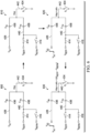
- FIG. 2 shows a schematic diagram of an AFE circuit 200.
- the AFE circuit 200 is an implementation of the AFE circuit 106.
- the AFE circuit 200 includes a programmable gain amplifier 202 and common mode amplifier 204 connected in a common mode loop.
- the programmable gain amplifier 202 is a differential amplifier having a non-inverting output 218, a non-inverting input 222, an inverting output 216, an inverting input 220, and a common mode input 214.
- the common mode input 214 is to receive a common mode output voltage to apply to the output signals produced at the inverting output 216 and the non-inverting output 218 of the programmable gain amplifier 202.
- the common mode amplifier 204 includes a non-inverting input 228, an inverting input 224, an inverting input 226, and an output 230.
- the inverting output 216 of the programmable gain amplifier 202 is coupled, via a first variable resistor 206, to the non-inverting input 222 of the programmable gain amplifier 202 and to the inverting input 224 of the common mode amplifier 204.
- the non-inverting output 218 of the programmable gain amplifier 202 is coupled, via a second variable resistor 206, to the inverting input 220 of the programmable gain amplifier 202 and to the inverting input 226 of the common mode amplifier 204.
- the resistance of the variable resistors 206 is variable to control the gain of the programmable gain amplifier 202.
- the AFE circuit 200 includes a signal input terminal 234 and a reference input terminal 232.
- the signal input terminal 234 is an example of the signal input terminal 114
- the reference input terminal 232 is an example of the reference input terminal 116.
- the signal input terminal 234 is coupled, via a first input resistor 210, to the inverting input 224 of the common mode amplifier 204, and to the non-inverting input 222 of the programmable gain amplifier 202.
- the reference input terminal 232 is coupled, via a second input resistor 210, to the inverting input 226 of the common mode amplifier 204, and to the inverting input 220 of the programmable gain amplifier 202.
- the resistor 210 has a resistance of about 1 megohm in some implementations of the AFE circuit 200. In other implementations of the AFE circuit 200, the resistor 210 has a different resistance value.
- the common mode input voltage terminal 212 of the AFE circuit 200 is connected to the non-inverting input 228 of the common mode amplifier 204.
- the common mode input voltage terminal 212 is to receive an input common mode voltage.
- the common mode amplifier 204 amplifies a difference of the input common mode voltage and an average of the signals received at the inverting input 224 and the inverting input 226.
- the average of the signals received at the inverting input 224 and the inverting input 226 is set equal to the input common mode voltage by the common mode feedback loop.
- the output 230 of the common mode amplifier 204 is coupled to the non-inverting input 222 of the programmable gain amplifier 202 by a resistor 208, and to the inverting input 220 of the programmable gain amplifier 202 by a resistor 208.
- the output 230 of the common mode amplifier 204 is also provided to the floating input detection circuitry 108 for use in detecting whether the signal input terminal 234 is floating. Signal provided by the common mode amplifier 204 on the output 230 is common mode and is rejected by the programmable gain amplifier 202.
- FIG. 3 shows an example a circuit equivalent to a portion (the common mode amplifier stage) of the AFE circuit 200.
- the equivalent circuit 300 includes an amplifier 304, a pair of resistors 310, a resistor 306, a resistor 308, a signal input terminal 334, a reference input terminal 332, an input common mode terminal 312, and an output common mode terminal 314.
- the input common mode terminal 312 is connected to the non-inverting input 328 of the amplifier 304.
- the resistor 308 couples the output signal input terminal 334 of the amplifier 304 to the inverting input 324 of the amplifier 304.
- the resistor 308 has resistance of one-half of the resistance of the resistor 208.
- the resistor 306 couples the output common mode terminal 314 to the inverting input 324 of the amplifier 304.
- the resistor 306 has resistance of one-half the resistance of the variable resistor 206.
- a first instance of the resistor 310 couples the signal input terminal 334 to the inverting input 324 of the amplifier 304.
- a second instance of the resistor 310 couples the reference input terminal 332 to the inverting input terminal 324 of the amplifier 304.
- the resistor 310 has the same resistance as the resistor 210.
- the signal at the output 330 of the amplifier 304 is the same as the signal at the output 230 of the amplifier 204.
- G F is the gain of the equivalent circuit 300 when the signal input terminal 234 is floating.
- Implementations of the data acquisition system 100 evaluate the gain of the equivalent circuit 300 (i.e., gain from V INCM to V X ) to determine whether the signal input terminal 114 is floating.
- the data acquisition system 100 evaluates the gain of the equivalent circuit 300 in the voltage domain by comparing a change in output voltage Vx ( ⁇ V X ) produced in response to a change in input common mode voltage V INCM ( ⁇ V INCM ) to a threshold voltage.
- the comparison of ⁇ V X to ⁇ V TH is referred to herein as fine float detection, which is further described below.
- FIG. 4 shows block diagram for an example of floating input detection circuitry 400 in accordance with this description.
- the floating input detection circuitry 400 is an implementation of the floating input detection circuitry 108.
- the floating input detection circuitry 400 includes coarse detection circuitry 428 and fine detection circuitry 430.
- the coarse detection circuitry 428 includes a digital-to-analog converter (DAC) 402, coarse comparator circuitry 404, and control circuitry 418.
- the fine detection circuitry 430 includes the DAC 402, a capacitive digital-to-analog converter (CDAC) 406, a fine comparator 408, reference voltage switching circuitry 444, a top plate switch 434, and the control circuitry 418.
- the reference voltage switching circuitry 444 includes a reference switch 414 and a reference switch 416.
- the reference switch 414 includes a first terminal 414A that is coupled to the bottom plate 438B of the capacitor 438 and a second terminal 414B that is coupled to a first reference voltage source 446.
- the reference switch 416 includes a first terminal 416A that is coupled to the bottom plate 438B of the capacitor 438 and a second terminal 416B that is coupled to a second reference voltage source 448.
- the top plate switch 434 includes a first terminal 434A that is coupled to the top plate 436T of the capacitor 436 and the top plate 438T of the capacitor 438, and a second terminal 434B that is coupled to ground.
- the fine comparator 408 includes a first input 408A that is coupled to the top plate 436T of the capacitor 436 and the top plate 438T of the capacitor 438, a second input 408B that is coupled to ground, and an output 408C that is coupled to an input 418E of the control circuitry 418.
- the control circuitry 418 is coupled to, and controls the operation of, the DAC 402, the coarse comparator circuitry 404, the reference switch 414, the reference switch 416, the top plate switch 434, and the fine comparator 408.
- the control circuitry 418 includes an output 418C that is coupled to an input 402D of the DAC 402, an output 418D that indicates whether the signal input terminal 114 is floating.
- the DAC 402 is a resistive DAC, a capacitive DAC, a current DAC, or other type of DAC in various implementations of the floating input detection circuitry 400. Outputs of the DAC 402 are connected to the AFE circuit 200 and the coarse comparator circuitry 404. The DAC 402 generates the common mode input voltage 420 provided to the AFE circuit 200. An output 402A of the DAC 402 is coupled to one of the programmable gain amplifier 202 or the common mode amplifier 204. The voltage of the common mode input voltage 420, generated by the DAC 402, is controlled by the control circuitry 418. The control circuitry 418 changes the voltage of the common mode input voltage 420 to evaluate the gain of the AFE circuit 200.
- the floating input detection circuitry 400 applies a coarse determination and a fine determination to identify the state of the signal input terminal 114.
- the coarse determination is provided by the coarse detection circuitry 428.
- the control circuitry 418 determines whether the signal input terminal 114 is driven by comparing the output signal 426 to two threshold values.
- the DAC 402 is coupled to the coarse comparator circuitry 404 and provides threshold voltage 422 and threshold voltage 424 to the coarse comparator circuitry 404.
- the coarse comparator circuitry 404 includes a comparator 410 and a comparator 412.
- the comparator 410 compares the output signal 426 generated by the common mode amplifier 204 to a high threshold voltage 422, provided by the DAC 402, and the comparator 412 compares the output signal 426 to a low threshold voltage 424 provided by the DAC 402.
- the comparator 410 includes a terminal 410A that is coupled to the output 230 of the common mode amplifier 204, and a terminal 410B that is coupled to an output 402B of the DAC 402.
- An output 410C of the comparator 410 is coupled to an input 418A of the control circuitry 418.
- the comparator 412 includes a terminal 412A that is coupled to the output 230 of the common mode amplifier 204, and a terminal 412B that is coupled to an output 402C of the DAC 402.
- An output 412C of the comparator 412 is coupled to an input 418B of the control circuitry 418.
- the output signal 426 will also have a large swing (e.g., from power supply rail to power supply rail). If the signal input terminal 234 is floating, then no current flows in the resistor 210 and the output signal 426 will be a predetermined voltage. Similarly, if the signal input terminal 234 is driven with a voltage that is the same as the input common mode voltage on the common mode input voltage terminal 212, then the output signal 426 will be the same predetermined voltage generated when the signal input terminal is floating.
- the threshold voltage 422 is higher than the predetermined voltage, and the threshold voltage 424 is lower than the predetermined.
- an output of the coarse comparator circuitry 404 indicates that the signal input terminal 234 is driven rather than floating. If the output signal 426 is not greater than the threshold voltage 422 or not less than the threshold voltage 424, then an output of the coarse comparator circuitry 404 indicates that the signal input terminal 234 is possibly floating.
- FIG. 5 shows an illustration of an example of coarse float detection in accordance with this description.
- the threshold voltage 422 and the threshold voltage 424 are set about the predetermined voltage 502. If the output signal 426 is greater than the threshold voltage 422 or less than the threshold voltage 424, then the output signal 426 falls in a first amplitude region 504 that indicates the signal input terminal 234 is not floating. However, if the output signal 426 is not greater than the threshold voltage 422 or less than the threshold voltage 424, then the output signal 426 falls in a second amplitude region 506 that indicates the signal input terminal 234 is possibly floating.
- Implementations of the floating input detection circuitry 400 first apply coarse determination to determine whether the signal input terminal 234 is not floating, and if the coarse determination is inconclusive, apply fine determination. Use of the two-state detection process (coarse determination followed by fine determination if coarse determination is inconclusive) allows for fast and low-power detection of floating inputs with a variety of input signals.
- the floating input detection circuitry 400 applies the fine detection circuitry 430 to determine whether the signal input terminal is driven.
- the control circuitry 418 determines whether the signal input terminal 114 is driven by evaluating the gain of common mode amplifier stage (i.e., the gain from V INCM to V X ) of the AFE circuit 200 or the equivalent circuit 300.
- the fine detection compares multiple samples of the output signal 426 to determine whether the signal input terminal 234 is floating or driven. Each sample of the output signal 426 is acquired with a different input common mode voltage 420 applied at the common mode input voltage terminal 212.
- the control circuitry 418 prior to acquiring a sample of the output signal 426, the control circuitry 418 generates control signals 432 that cause the DAC 402 to change the common mode input voltage 420 applied at the common mode input voltage terminal 212. Changing the common mode input voltage 420 does not affect the differential output of the AFE circuit 200 because the common mode input voltage 420 is rejected as common mode. In conjunction with setting the common mode input voltage 420, the control circuitry 418 closes one of the reference switch 414 and the reference switch 416 provide a reference voltage to the CDAC 406.
- the CDAC 406 includes a capacitor 436 and a capacitor 438.
- the capacitor 436 has a bottom plate 436B that is coupled to the output 230 of the common mode amplifier 204 and a top plate 436T that is coupled to the comparator 408.
- the capacitor 438 has a bottom plate 438B that is coupled to the reference voltage switching circuitry 444 and a top plate 438T that is coupled to the comparator 408 and the top plate 436T of the capacitor 436.
- the control circuitry 418 closes the top plate switch 434 (i.e., connects the top plate 436T of the first capacitor 436 and the top plate 438T of the second capacitor 438 to ground) to charge the capacitor 436 of the CDAC 406 to the voltage of the output signal 426 and to charge the capacitor 438 of the CDAC 406 to the reference voltage 440 provided via the reference switch 414 or the reference switch 416. Thereafter, the top plate switch 434 is opened, the common mode input voltage 420 is changed, and reference voltage 440 is changed by changing which of the reference switch 414 and the reference switch 416 is closed.
- the output (i.e., the top plate voltage 442) of the CDAC 406 is: ⁇ ⁇ V Xmeas ⁇ ⁇ V TH where: ⁇ is an attenuation factor;
- FIG. 6 shows an example of fine float detection in accordance with this description.
- configuration 600 the common mode input voltage 420 has been set, and the reference switch 414, the reference switch 416, and the top plate switch 434 are set to acquire a sample of the output signal 426 and the reference voltage 440. Selection of which of the reference switch 414 and the reference switch 416 are closed in the configuration 600 is based on the direction of change to be produced in the common mode input voltage 420 in configuration 620. If the voltage of the common mode input voltage 420 is to be increased in the configuration 620, then the reference switch 414 is closed and the reference switch 416 is open in the configuration 600. Similarly, if the voltage of the common mode input voltage 420 is to be decreased in the configuration 620, then the reference switch 416 is closed and the reference switch 414 is open in the configuration 600.
- the top plate switch 434 is opened to disconnect the top plate 436T of capacitor 436 and the top plate 438T of the capacitor 438 from ground.
- the common mode input voltage 420 is changed (e.g., increased). That is the control circuitry 418 provides the control signals 432 to the DAC 402 which changes the common mode input voltage 420, and in turn, changes the output signal 426.
- the top plate voltage 442 is: C IN C IN + C TH V X 2 ⁇ V X 1 where:
- the control circuitry 418 opens the reference switch 414 and closes the reference switch 416 to change the reference voltage 440 provided to the capacitor 438.
- the top plate voltage 442 is: C IN C IN + C TH V X 2 ⁇ V X 1 + C TH C IN + C TH V REFP ⁇ V REFM where:
- the fine comparator 408 compares the top plate voltage 442 to ground to determine whether the gain from V INCM to V X (in the AFE circuit 200 or the equivalent circuit 300) exceeds a predetermined gain value (e.g., a gain value corresponding to the gain from V INCM to Vx if the signal input terminal 234 is floating).
- a predetermined gain value e.g., a gain value corresponding to the gain from V INCM to Vx if the signal input terminal 234 is floating.
- the control circuitry 418 changes the common mode input voltage 420 pseudo-randomly and/or performs multiple iterations of comparison of two different values of the output signal 426 to ensure that changes in the common mode input voltage 420 does not follow any signal voltage that is present at the signal input terminal 234.
- the control circuitry 418 avoids false detection of the signal input terminal 234 as floating.
- FIG. 7 shows a flow diagram for a method 700 for floating input detection in accordance with this description. Though depicted sequentially as a matter of convenience, at least some of the actions shown can be performed in a different order and/or performed in parallel. Additionally, some implementations may perform only some of the actions shown. Operations of the method 700 may be performed by implementations of the data acquisition system 100.
- the floating input detection circuitry 108 is set to a base or reset state.
- a float indicator (e.g., a float flag bit) corresponding to the signal input terminal 234 is reset.
- a common mode input voltage 420 is provided to the common mode amplifier 204.
- the switches 414, 416, and 424 are set as per the configuration 600.
- An output signal 426 generated by the common mode amplifier 204 is provided to the coarse detection circuitry 428, the fine detection circuitry 430, the non-inverting input 222 of the programmable gain amplifier 202, and the inverting input 220 of the programmable gain amplifier 202.
- the floating input detection circuitry 108 performs a coarse detection to determine whether the signal input terminal 234 is driven.
- the coarse detection includes comparing the output signal 426 generated by the common mode amplifier 204 to a threshold voltage 422 and a threshold voltage 424.
- the control circuitry 418 continues floating input detection by going back to block 702.
- the signal input terminal 234 is determined to be driven if the output of the common mode amplifier 204 is greater than the threshold voltage 422 or less than the threshold voltage 424.
- the floating input detection circuitry 108 performs fine detection in block 708 to determine whether the common mode amplifier stage (e.g., the equivalent circuit 300) indicates that the signal input terminal 234 is floating.
- the fine detection includes repetitively acquiring a sample of the output signal 436 and a sample of a reference voltage 440 on the CDAC 406.
- the common mode input voltage 420 and the reference voltage 440 is changed for each iteration of the fine detection.
- the top plate voltage 442 of the CDAC 406 is compared to ground.
- control circuitry 418 continues floating input detection by going back to block 702.
- the floating input detection circuitry 108 determines whether the fine detection of block 708 has been executed a predetermined number of times. If the fine detection of block 708 has been executed a predetermined number of times, each time indicating that the signal input terminal 234 is floating, then the float indicator for the signal input terminal 234 is set in block 714. If the fine detection of block 708 has not been executed the predetermined number of times, then fine detection continues in block 708. Requiring that multiple consecutive fine detections indicate that the signal input terminal 234 is floating reduces false detection of a floating condition.
- FIG. 8 shows a schematic diagram of a second example of an AFE circuit 800 that is suitable for use in detecting a floating input in accordance with this description.
- the AFE circuit 800 is an implementation of the AFE circuit 106.
- the AFE circuit 800 includes a programmable gain amplifier 802 and common mode amplifier 804 connected in a common mode loop.
- the AFE circuit 800 senses the common mode voltage at the output of the programmable gain amplifier 802 and corrects the common mode voltage via the common mode loop.
- the transfer function difference from V INCM to V X is used by the floating input detection circuitry 400 determine whether the signal input terminal 234 is floating.
- the programmable gain amplifier 802 is a differential amplifier having a non-inverting output 818, a non-inverting input 822, an inverting output 816, an inverting input 820, and a common mode input 814.
- the common mode input 814 is to receive a common mode input voltage and is coupled to the common mode input 214.
- the common mode amplifier 804 includes a non-inverting input 828, an inverting input 824, and an output 830.
- the inverting output 816 of the programmable gain amplifier 802 is coupled, via a first variable resistor 806, to the non-inverting input 822 of the programmable gain amplifier 802 and, via a first resistor 826, to the non-inverting input 828 of the common mode amplifier 804.
- the non-inverting output 818 of the programmable gain amplifier 802 is coupled, via a second variable resistor 806, to the inverting input 820 of the programmable gain amplifier 802, and, via a second resistor 826, to the non-inverting input 828 of the common mode amplifier 804.
- the resistance of the variable resistors 806 is variable to control the gain of the programmable gain amplifier 802.
- the AFE circuit 800 includes a signal input terminal 234 and a reference input terminal 232.
- the signal input terminal 234 is an example of the signal input terminal 114
- the reference input terminal 232 is an example of the reference input terminal 116.
- the signal input terminal 234 is coupled, via a first input resistor 810, to the non-inverting input 822 of the programmable gain amplifier 802.
- the reference input terminal 232 is coupled, via a second input resistor 810, to the inverting input 820 of the programmable gain amplifier 802.
- the resistors 826 are coupled to the non-inverting input 828 of the common mode amplifier 804, and average signal received from the inverting output 816 and the non-inverting output 818 of the programmable gain amplifier 802.
- the common mode amplifier 804 amplifies a difference of the output common mode voltage received at the inverting input 824 and an average of the signals received from the programmable gain amplifier 802.
- the output 830 of the common mode amplifier 804 is coupled to the non-inverting input 822 of the programmable gain amplifier 802 by a resistor 808, and to the inverting input 820 of the programmable gain amplifier 802 by a resistor 808.
- the output 830 of the common mode amplifier 804 is also provided to the floating input detection circuitry 108 for use in detecting whether the signal input terminal 834 is floating. Signal provided by the common mode amplifier 804 on the output 830 is common mode and is rejected by the programmable gain amplifier 802.
- FIG. 9 shows a schematic diagram of a third example of an AFE circuit 900 that is suitable for use in detecting a floating input in accordance with this description.
- the AFE circuit 900 is an implementation of the AFE circuit 106.
- the AFE circuit 900 includes a programmable gain amplifier 902 and common mode amplifier 904 connected in a common mode loop.
- the AFE circuit 900 senses the common mode voltage at the input terminals 232 and 234 and corrects the common mode voltage via a feedforward path.
- the transfer function difference from V INCM to V X is used by the floating input detection circuitry 400 determine whether the signal input terminal 234 is floating.
- the programmable gain amplifier 902 is a differential amplifier having a non-inverting output 918, a non-inverting input 922, an inverting output 916, an inverting input 920, and a common mode input 914.
- the common mode input 914 is to receive a common mode output voltage to apply to the output signals produced at the inverting output 916 and the non-inverting output 918 of the programmable gain amplifier 902.
- the common mode amplifier 904 includes an inverting input 928, a non-inverting input 924, and an output 930.
- the inverting output 916 of the programmable gain amplifier 902 is coupled, via a first variable resistor 906, to the non-inverting input 922 of the programmable gain amplifier 902 and, via a resistor 926, to the inverting input 928 of the common mode amplifier 904.
- the non-inverting output 918 of the programmable gain amplifier 902 is coupled, via a second variable resistor 906, to the inverting input 920 of the programmable gain amplifier 902, and, via a second resistor 926, to the inverting input 928 of the common mode amplifier 904.
- the resistance of the variable resistors 906 is variable to control the gain of the programmable gain amplifier 902.
- the AFE circuit 900 includes a signal input terminal 234 and a reference input terminal 232.
- the signal input terminal 234 is an example of the signal input terminal 114
- the reference input terminal 232 is an example of the reference input terminal 116.
- the signal input terminal 234 is coupled, via a first input resistor 910, to the non-inverting input 922 of the programmable gain amplifier 902.
- the reference input terminal 232 is coupled, via a second input resistor 910, to the inverting input 920 of the programmable gain amplifier 902.
- the resistors 926 are coupled to the inverting input 928 of the common mode amplifier 904, and average signal at the signal input terminal 234 and the reference input terminal 232.
- the common mode amplifier 904 amplifies a difference of the output common mode voltage received at the non-inverting input 924 and an average of the signals received from the programmable gain amplifier 902.
- the output 930 of the common mode amplifier 904 is coupled to the inverting input 928 of the common mode amplifier 904 by a resistor 912, to the non-inverting input 922 of the programmable gain amplifier 902 by a resistor 908, and to the inverting input 920 of the programmable gain amplifier 902 by a resistor 908.
- the output 930 of the common mode amplifier 904 is also provided to the floating input detection circuitry 108 for use in detecting whether the signal input terminal 934 is floating. Signal provided by the common mode amplifier 904 on the output 930 is common mode and is rejected by the programmable gain amplifier 902.
Landscapes
- Engineering & Computer Science (AREA)
- Power Engineering (AREA)
- Physics & Mathematics (AREA)
- Nonlinear Science (AREA)
- Analogue/Digital Conversion (AREA)
- Manipulation Of Pulses (AREA)
- Amplifiers (AREA)
- General Physics & Mathematics (AREA)
Applications Claiming Priority (3)
| Application Number | Priority Date | Filing Date | Title |
|---|---|---|---|
| IN201841011581 | 2018-03-28 | ||
| US16/124,261 US10725118B2 (en) | 2018-03-28 | 2018-09-07 | Floating input detection |
| PCT/US2019/024500 WO2019191377A1 (en) | 2018-03-28 | 2019-03-28 | Floating input detection |
Publications (3)
| Publication Number | Publication Date |
|---|---|
| EP3776863A1 EP3776863A1 (en) | 2021-02-17 |
| EP3776863A4 EP3776863A4 (en) | 2021-06-09 |
| EP3776863B1 true EP3776863B1 (en) | 2024-03-13 |
Family
ID=68054883
Family Applications (1)
| Application Number | Title | Priority Date | Filing Date |
|---|---|---|---|
| EP19774325.5A Active EP3776863B1 (en) | 2018-03-28 | 2019-03-28 | Floating input detection |
Country Status (5)
| Country | Link |
|---|---|
| US (1) | US10725118B2 (https=) |
| EP (1) | EP3776863B1 (https=) |
| JP (1) | JP7597985B2 (https=) |
| CN (1) | CN111788775B (https=) |
| WO (1) | WO2019191377A1 (https=) |
Families Citing this family (3)
| Publication number | Priority date | Publication date | Assignee | Title |
|---|---|---|---|---|
| CN110703125A (zh) * | 2019-08-12 | 2020-01-17 | 苏州市职业大学 | 一种plc端子检测装置和检测方法 |
| US11621686B2 (en) * | 2021-01-26 | 2023-04-04 | Infineon Technologies Ag | Gray zone prevention circuit with indirect signal monitoring |
| TWI887012B (zh) * | 2024-06-21 | 2025-06-11 | 大陸商北京集創北方科技股份有限公司 | 晶片輸出電流設定電路、顯示驅動晶片及顯示器 |
Family Cites Families (31)
| Publication number | Priority date | Publication date | Assignee | Title |
|---|---|---|---|---|
| US4166243A (en) * | 1978-04-21 | 1979-08-28 | General Motors Corporation | Thermocouple failure detector |
| JPS63234756A (ja) * | 1987-03-24 | 1988-09-30 | Toshiba Corp | 端末インタフエ−ス回路 |
| US5161175A (en) | 1991-05-28 | 1992-11-03 | Motorola, Inc. | Circuit and method of detecting an invalid clock signal |
| KR950004637B1 (ko) | 1993-01-19 | 1995-05-03 | 삼성전자주식회사 | 플로우팅 감지 회로 |
| US5418453A (en) * | 1993-11-09 | 1995-05-23 | Delco Electronics Corporation | Method of measuring wheel speed sensor impedance |
| JPH1032439A (ja) * | 1996-07-17 | 1998-02-03 | Nippon Columbia Co Ltd | 平衡増幅回路 |
| JP3595483B2 (ja) | 2000-01-27 | 2004-12-02 | Necエレクトロニクス株式会社 | 電荷検出信号処理回路 |
| US6833759B2 (en) * | 2002-01-23 | 2004-12-21 | Broadcom Corporation | System and method for a programmable gain amplifier |
| US7233473B2 (en) * | 2002-11-18 | 2007-06-19 | Nxp B.V. | Protection circuit and method for floating power transfer device |
| JP3994912B2 (ja) * | 2003-05-09 | 2007-10-24 | 株式会社デンソー | センサ回路 |
| JP2008103793A (ja) * | 2006-10-17 | 2008-05-01 | Sony Corp | 撮像装置、信号処理装置、および信号処理方法、並びにコンピュータ・プログラム |
| JP5144704B2 (ja) * | 2010-03-25 | 2013-02-13 | 日本電信電話株式会社 | 差動トランスインピーダンス増幅器 |
| US8330537B1 (en) * | 2010-07-23 | 2012-12-11 | National Semiconductor Corporation | Low noise, high CMRR and PSRR input buffer |
| CN101917171A (zh) * | 2010-08-19 | 2010-12-15 | 华东师范大学 | 基于运算放大器的宽带可编程增益放大器 |
| US10473731B2 (en) * | 2010-11-26 | 2019-11-12 | Stmicroelectronics S.R.L. | Magnetic sensor reading device, system and method |
| US8390374B2 (en) * | 2011-01-25 | 2013-03-05 | Analog Devices, Inc. | Apparatus and method for amplification with high front-end gain in the presence of large DC offsets |
| US8686889B2 (en) * | 2011-09-16 | 2014-04-01 | Conexant Systems, Inc. | Analog frontend for CCD/CIS sensor |
| US8878570B2 (en) * | 2011-09-30 | 2014-11-04 | Silicon Laboratories Inc. | Configurable analog front end |
| US8587461B1 (en) | 2011-10-27 | 2013-11-19 | Maxim Integrated Products, Inc. | Data acquisition system with analog-to-digital converter having integrated multiplexer control |
| US8742968B2 (en) * | 2011-11-11 | 2014-06-03 | Microchip Technology Incorporated | Analog front end device with two-wire interface |
| JP5891811B2 (ja) * | 2012-01-24 | 2016-03-23 | セイコーエプソン株式会社 | 全差動増幅回路、コンパレーター回路、a/d変換回路、及び電子機器 |
| US9083892B2 (en) * | 2012-03-01 | 2015-07-14 | Nikon Corporation | A/D conversion circuit, and solid-state image pickup apparatus |
| JP5733276B2 (ja) * | 2012-07-13 | 2015-06-10 | 株式会社デンソー | 静電容量型センサの検出回路 |
| US10101403B2 (en) * | 2014-07-02 | 2018-10-16 | Intersil Americas LLC | Systems and methods for an open wire scan |
| CN104283519B (zh) * | 2014-10-24 | 2017-06-09 | 中国电子科技集团公司第十三研究所 | 电流复用型前馈补偿全差分运算放大器 |
| US9846569B1 (en) * | 2014-11-17 | 2017-12-19 | Seagate Technology Llc | Random values based on a random components of noise |
| CN104639168B (zh) * | 2015-02-15 | 2017-11-10 | 芯原微电子(上海)有限公司 | Sigma‑Delta型模数转换器模拟前端电路 |
| US9706269B2 (en) * | 2015-07-24 | 2017-07-11 | Hong Kong Applied Science and Technology Research Institute Company, Limited | Self-powered and battery-assisted CMOS wireless bio-sensing IC platform |
| DE102015116786A1 (de) * | 2015-10-02 | 2017-04-06 | Infineon Technologies Ag | Vorrichtungsverfahren zum Testen eines Analog-Digital Wandlers |
| CN106850055B (zh) * | 2016-12-28 | 2019-01-18 | 上海交通大学 | 一种用于光纤瞬断检测系统的宽带低噪声模拟前端电路 |
| CN106877830B (zh) * | 2017-04-06 | 2023-05-02 | 上海芯问科技有限公司 | 一种用于生理电势信号检测的模拟前端电路 |
-
2018
- 2018-09-07 US US16/124,261 patent/US10725118B2/en active Active
-
2019
- 2019-03-28 WO PCT/US2019/024500 patent/WO2019191377A1/en not_active Ceased
- 2019-03-28 JP JP2020552245A patent/JP7597985B2/ja active Active
- 2019-03-28 EP EP19774325.5A patent/EP3776863B1/en active Active
- 2019-03-28 CN CN201980016209.8A patent/CN111788775B/zh active Active
Also Published As
| Publication number | Publication date |
|---|---|
| US10725118B2 (en) | 2020-07-28 |
| JP7597985B2 (ja) | 2024-12-11 |
| JP2021520094A (ja) | 2021-08-12 |
| CN111788775B (zh) | 2024-05-14 |
| WO2019191377A1 (en) | 2019-10-03 |
| CN111788775A (zh) | 2020-10-16 |
| EP3776863A4 (en) | 2021-06-09 |
| US20190302163A1 (en) | 2019-10-03 |
| EP3776863A1 (en) | 2021-02-17 |
Similar Documents
| Publication | Publication Date | Title |
|---|---|---|
| EP3776863B1 (en) | Floating input detection | |
| US8884629B1 (en) | Background sensor diagnostic for multi-channel ADC | |
| US6940271B2 (en) | Pin electronics interface circuit | |
| EP1688750A1 (en) | Differential termination and attenuator network for a measurement probe having an automated common mode termination voltage generator | |
| US11249117B2 (en) | Autoranging ammeter with fast dynamic response | |
| DE112017000503T5 (de) | Kapazitäts-Messschaltung mit Sensorverdrahtungsdiagnose | |
| US10359449B2 (en) | Current measurement techniques to compensate for shunt drift | |
| EP1894302B1 (en) | Rapid response current measurement system and method | |
| CN105680864B (zh) | 逐次逼近模数转换器、模数转换方法和传感信号处理装置 | |
| CN111190047B (zh) | 一种电流采集诊断电路及其失效诊断方法 | |
| CN110118899B (zh) | 检测差分信号链的故障状况和信道不平衡的方法和设备 | |
| CN111175559B (zh) | 多级电流测量架构 | |
| JP3129820B2 (ja) | 粒子検出装置 | |
| WO2009020566A1 (en) | Voltage transformation circuit | |
| US20060273811A1 (en) | Using an active load as a high current output stage of a precision pin measurement unit in automatic test equipment systems | |
| US11402275B2 (en) | Sensor apparatus | |
| JPH0645909Y2 (ja) | Ic試験装置 | |
| US6766264B2 (en) | Method and apparatus for calibrating parameters to be used in a digital circuit simulation | |
| US20230266371A1 (en) | Impedance measurement | |
| JP3562703B2 (ja) | 計測装置 | |
| US11774469B2 (en) | Auto ranging ammeter with accurate measurement during range changes | |
| US12461131B2 (en) | Device inspection apparatus and device inspection method | |
| JP4310280B2 (ja) | インピーダンス変換回路、入出力回路及び半導体試験装置 | |
| Kasin | Is Your Data Inaccurate Because of Instrumentation Amplifier Settling Time? | |
| CN121008702A (zh) | 用于检测触摸显示面板损坏的方法 |
Legal Events
| Date | Code | Title | Description |
|---|---|---|---|
| STAA | Information on the status of an ep patent application or granted ep patent |
Free format text: STATUS: THE INTERNATIONAL PUBLICATION HAS BEEN MADE |
|
| PUAI | Public reference made under article 153(3) epc to a published international application that has entered the european phase |
Free format text: ORIGINAL CODE: 0009012 |
|
| STAA | Information on the status of an ep patent application or granted ep patent |
Free format text: STATUS: REQUEST FOR EXAMINATION WAS MADE |
|
| 17P | Request for examination filed |
Effective date: 20201028 |
|
| AK | Designated contracting states |
Kind code of ref document: A1 Designated state(s): AL AT BE BG CH CY CZ DE DK EE ES FI FR GB GR HR HU IE IS IT LI LT LU LV MC MK MT NL NO PL PT RO RS SE SI SK SM TR |
|
| AX | Request for extension of the european patent |
Extension state: BA ME |
|
| A4 | Supplementary search report drawn up and despatched |
Effective date: 20210507 |
|
| RIC1 | Information provided on ipc code assigned before grant |
Ipc: H03M 1/66 20060101AFI20210430BHEP Ipc: H03F 3/45 20060101ALI20210430BHEP Ipc: G01R 31/50 20200101ALI20210430BHEP |
|
| DAV | Request for validation of the european patent (deleted) | ||
| DAX | Request for extension of the european patent (deleted) | ||
| GRAP | Despatch of communication of intention to grant a patent |
Free format text: ORIGINAL CODE: EPIDOSNIGR1 |
|
| STAA | Information on the status of an ep patent application or granted ep patent |
Free format text: STATUS: GRANT OF PATENT IS INTENDED |
|
| INTG | Intention to grant announced |
Effective date: 20231006 |
|
| P01 | Opt-out of the competence of the unified patent court (upc) registered |
Effective date: 20231107 |
|
| GRAS | Grant fee paid |
Free format text: ORIGINAL CODE: EPIDOSNIGR3 |
|
| GRAA | (expected) grant |
Free format text: ORIGINAL CODE: 0009210 |
|
| STAA | Information on the status of an ep patent application or granted ep patent |
Free format text: STATUS: THE PATENT HAS BEEN GRANTED |
|
| AK | Designated contracting states |
Kind code of ref document: B1 Designated state(s): AL AT BE BG CH CY CZ DE DK EE ES FI FR GB GR HR HU IE IS IT LI LT LU LV MC MK MT NL NO PL PT RO RS SE SI SK SM TR |
|
| REG | Reference to a national code |
Ref country code: GB Ref legal event code: FG4D |
|
| REG | Reference to a national code |
Ref country code: CH Ref legal event code: EP |
|
| REG | Reference to a national code |
Ref country code: DE Ref legal event code: R096 Ref document number: 602019048251 Country of ref document: DE |
|
| REG | Reference to a national code |
Ref country code: IE Ref legal event code: FG4D |
|
| PG25 | Lapsed in a contracting state [announced via postgrant information from national office to epo] |
Ref country code: LT Free format text: LAPSE BECAUSE OF FAILURE TO SUBMIT A TRANSLATION OF THE DESCRIPTION OR TO PAY THE FEE WITHIN THE PRESCRIBED TIME-LIMIT Effective date: 20240313 |
|
| REG | Reference to a national code |
Ref country code: LT Ref legal event code: MG9D |
|
| PG25 | Lapsed in a contracting state [announced via postgrant information from national office to epo] |
Ref country code: GR Free format text: LAPSE BECAUSE OF FAILURE TO SUBMIT A TRANSLATION OF THE DESCRIPTION OR TO PAY THE FEE WITHIN THE PRESCRIBED TIME-LIMIT Effective date: 20240614 |
|
| REG | Reference to a national code |
Ref country code: NL Ref legal event code: MP Effective date: 20240313 |
|
| PG25 | Lapsed in a contracting state [announced via postgrant information from national office to epo] |
Ref country code: RS Free format text: LAPSE BECAUSE OF FAILURE TO SUBMIT A TRANSLATION OF THE DESCRIPTION OR TO PAY THE FEE WITHIN THE PRESCRIBED TIME-LIMIT Effective date: 20240613 Ref country code: HR Free format text: LAPSE BECAUSE OF FAILURE TO SUBMIT A TRANSLATION OF THE DESCRIPTION OR TO PAY THE FEE WITHIN THE PRESCRIBED TIME-LIMIT Effective date: 20240313 |
|
| PG25 | Lapsed in a contracting state [announced via postgrant information from national office to epo] |
Ref country code: ES Free format text: LAPSE BECAUSE OF FAILURE TO SUBMIT A TRANSLATION OF THE DESCRIPTION OR TO PAY THE FEE WITHIN THE PRESCRIBED TIME-LIMIT Effective date: 20240313 |
|
| PG25 | Lapsed in a contracting state [announced via postgrant information from national office to epo] |
Ref country code: RS Free format text: LAPSE BECAUSE OF FAILURE TO SUBMIT A TRANSLATION OF THE DESCRIPTION OR TO PAY THE FEE WITHIN THE PRESCRIBED TIME-LIMIT Effective date: 20240613 Ref country code: NO Free format text: LAPSE BECAUSE OF FAILURE TO SUBMIT A TRANSLATION OF THE DESCRIPTION OR TO PAY THE FEE WITHIN THE PRESCRIBED TIME-LIMIT Effective date: 20240613 Ref country code: LT Free format text: LAPSE BECAUSE OF FAILURE TO SUBMIT A TRANSLATION OF THE DESCRIPTION OR TO PAY THE FEE WITHIN THE PRESCRIBED TIME-LIMIT Effective date: 20240313 Ref country code: HR Free format text: LAPSE BECAUSE OF FAILURE TO SUBMIT A TRANSLATION OF THE DESCRIPTION OR TO PAY THE FEE WITHIN THE PRESCRIBED TIME-LIMIT Effective date: 20240313 Ref country code: GR Free format text: LAPSE BECAUSE OF FAILURE TO SUBMIT A TRANSLATION OF THE DESCRIPTION OR TO PAY THE FEE WITHIN THE PRESCRIBED TIME-LIMIT Effective date: 20240614 Ref country code: FI Free format text: LAPSE BECAUSE OF FAILURE TO SUBMIT A TRANSLATION OF THE DESCRIPTION OR TO PAY THE FEE WITHIN THE PRESCRIBED TIME-LIMIT Effective date: 20240313 Ref country code: ES Free format text: LAPSE BECAUSE OF FAILURE TO SUBMIT A TRANSLATION OF THE DESCRIPTION OR TO PAY THE FEE WITHIN THE PRESCRIBED TIME-LIMIT Effective date: 20240313 Ref country code: BG Free format text: LAPSE BECAUSE OF FAILURE TO SUBMIT A TRANSLATION OF THE DESCRIPTION OR TO PAY THE FEE WITHIN THE PRESCRIBED TIME-LIMIT Effective date: 20240313 |
|
| REG | Reference to a national code |
Ref country code: AT Ref legal event code: MK05 Ref document number: 1666715 Country of ref document: AT Kind code of ref document: T Effective date: 20240313 |
|
| PG25 | Lapsed in a contracting state [announced via postgrant information from national office to epo] |
Ref country code: SE Free format text: LAPSE BECAUSE OF FAILURE TO SUBMIT A TRANSLATION OF THE DESCRIPTION OR TO PAY THE FEE WITHIN THE PRESCRIBED TIME-LIMIT Effective date: 20240313 Ref country code: LV Free format text: LAPSE BECAUSE OF FAILURE TO SUBMIT A TRANSLATION OF THE DESCRIPTION OR TO PAY THE FEE WITHIN THE PRESCRIBED TIME-LIMIT Effective date: 20240313 |
|
| PG25 | Lapsed in a contracting state [announced via postgrant information from national office to epo] |
Ref country code: NL Free format text: LAPSE BECAUSE OF FAILURE TO SUBMIT A TRANSLATION OF THE DESCRIPTION OR TO PAY THE FEE WITHIN THE PRESCRIBED TIME-LIMIT Effective date: 20240313 |
|
| PG25 | Lapsed in a contracting state [announced via postgrant information from national office to epo] |
Ref country code: NL Free format text: LAPSE BECAUSE OF FAILURE TO SUBMIT A TRANSLATION OF THE DESCRIPTION OR TO PAY THE FEE WITHIN THE PRESCRIBED TIME-LIMIT Effective date: 20240313 |
|
| PG25 | Lapsed in a contracting state [announced via postgrant information from national office to epo] |
Ref country code: IS Free format text: LAPSE BECAUSE OF FAILURE TO SUBMIT A TRANSLATION OF THE DESCRIPTION OR TO PAY THE FEE WITHIN THE PRESCRIBED TIME-LIMIT Effective date: 20240713 |
|
| PG25 | Lapsed in a contracting state [announced via postgrant information from national office to epo] |
Ref country code: SM Free format text: LAPSE BECAUSE OF FAILURE TO SUBMIT A TRANSLATION OF THE DESCRIPTION OR TO PAY THE FEE WITHIN THE PRESCRIBED TIME-LIMIT Effective date: 20240313 Ref country code: PT Free format text: LAPSE BECAUSE OF FAILURE TO SUBMIT A TRANSLATION OF THE DESCRIPTION OR TO PAY THE FEE WITHIN THE PRESCRIBED TIME-LIMIT Effective date: 20240715 |
|
| PG25 | Lapsed in a contracting state [announced via postgrant information from national office to epo] |
Ref country code: CZ Free format text: LAPSE BECAUSE OF FAILURE TO SUBMIT A TRANSLATION OF THE DESCRIPTION OR TO PAY THE FEE WITHIN THE PRESCRIBED TIME-LIMIT Effective date: 20240313 Ref country code: EE Free format text: LAPSE BECAUSE OF FAILURE TO SUBMIT A TRANSLATION OF THE DESCRIPTION OR TO PAY THE FEE WITHIN THE PRESCRIBED TIME-LIMIT Effective date: 20240313 |
|
| PG25 | Lapsed in a contracting state [announced via postgrant information from national office to epo] |
Ref country code: AT Free format text: LAPSE BECAUSE OF FAILURE TO SUBMIT A TRANSLATION OF THE DESCRIPTION OR TO PAY THE FEE WITHIN THE PRESCRIBED TIME-LIMIT Effective date: 20240313 |
|
| PG25 | Lapsed in a contracting state [announced via postgrant information from national office to epo] |
Ref country code: PL Free format text: LAPSE BECAUSE OF FAILURE TO SUBMIT A TRANSLATION OF THE DESCRIPTION OR TO PAY THE FEE WITHIN THE PRESCRIBED TIME-LIMIT Effective date: 20240313 |
|
| PG25 | Lapsed in a contracting state [announced via postgrant information from national office to epo] |
Ref country code: SK Free format text: LAPSE BECAUSE OF FAILURE TO SUBMIT A TRANSLATION OF THE DESCRIPTION OR TO PAY THE FEE WITHIN THE PRESCRIBED TIME-LIMIT Effective date: 20240313 |
|
| PG25 | Lapsed in a contracting state [announced via postgrant information from national office to epo] |
Ref country code: SM Free format text: LAPSE BECAUSE OF FAILURE TO SUBMIT A TRANSLATION OF THE DESCRIPTION OR TO PAY THE FEE WITHIN THE PRESCRIBED TIME-LIMIT Effective date: 20240313 Ref country code: SK Free format text: LAPSE BECAUSE OF FAILURE TO SUBMIT A TRANSLATION OF THE DESCRIPTION OR TO PAY THE FEE WITHIN THE PRESCRIBED TIME-LIMIT Effective date: 20240313 Ref country code: RO Free format text: LAPSE BECAUSE OF FAILURE TO SUBMIT A TRANSLATION OF THE DESCRIPTION OR TO PAY THE FEE WITHIN THE PRESCRIBED TIME-LIMIT Effective date: 20240313 Ref country code: PT Free format text: LAPSE BECAUSE OF FAILURE TO SUBMIT A TRANSLATION OF THE DESCRIPTION OR TO PAY THE FEE WITHIN THE PRESCRIBED TIME-LIMIT Effective date: 20240715 Ref country code: PL Free format text: LAPSE BECAUSE OF FAILURE TO SUBMIT A TRANSLATION OF THE DESCRIPTION OR TO PAY THE FEE WITHIN THE PRESCRIBED TIME-LIMIT Effective date: 20240313 Ref country code: IS Free format text: LAPSE BECAUSE OF FAILURE TO SUBMIT A TRANSLATION OF THE DESCRIPTION OR TO PAY THE FEE WITHIN THE PRESCRIBED TIME-LIMIT Effective date: 20240713 Ref country code: EE Free format text: LAPSE BECAUSE OF FAILURE TO SUBMIT A TRANSLATION OF THE DESCRIPTION OR TO PAY THE FEE WITHIN THE PRESCRIBED TIME-LIMIT Effective date: 20240313 Ref country code: CZ Free format text: LAPSE BECAUSE OF FAILURE TO SUBMIT A TRANSLATION OF THE DESCRIPTION OR TO PAY THE FEE WITHIN THE PRESCRIBED TIME-LIMIT Effective date: 20240313 Ref country code: AT Free format text: LAPSE BECAUSE OF FAILURE TO SUBMIT A TRANSLATION OF THE DESCRIPTION OR TO PAY THE FEE WITHIN THE PRESCRIBED TIME-LIMIT Effective date: 20240313 |
|
| REG | Reference to a national code |
Ref country code: CH Ref legal event code: PL |
|
| PG25 | Lapsed in a contracting state [announced via postgrant information from national office to epo] |
Ref country code: LU Free format text: LAPSE BECAUSE OF NON-PAYMENT OF DUE FEES Effective date: 20240328 |
|
| PG25 | Lapsed in a contracting state [announced via postgrant information from national office to epo] |
Ref country code: LU Free format text: LAPSE BECAUSE OF NON-PAYMENT OF DUE FEES Effective date: 20240328 |
|
| PG25 | Lapsed in a contracting state [announced via postgrant information from national office to epo] |
Ref country code: IT Free format text: LAPSE BECAUSE OF FAILURE TO SUBMIT A TRANSLATION OF THE DESCRIPTION OR TO PAY THE FEE WITHIN THE PRESCRIBED TIME-LIMIT Effective date: 20240313 |
|
| REG | Reference to a national code |
Ref country code: DE Ref legal event code: R097 Ref document number: 602019048251 Country of ref document: DE Ref country code: BE Ref legal event code: MM Effective date: 20240331 |
|
| PG25 | Lapsed in a contracting state [announced via postgrant information from national office to epo] |
Ref country code: IT Free format text: LAPSE BECAUSE OF FAILURE TO SUBMIT A TRANSLATION OF THE DESCRIPTION OR TO PAY THE FEE WITHIN THE PRESCRIBED TIME-LIMIT Effective date: 20240313 |
|
| PG25 | Lapsed in a contracting state [announced via postgrant information from national office to epo] |
Ref country code: MC Free format text: LAPSE BECAUSE OF FAILURE TO SUBMIT A TRANSLATION OF THE DESCRIPTION OR TO PAY THE FEE WITHIN THE PRESCRIBED TIME-LIMIT Effective date: 20240313 |
|
| PG25 | Lapsed in a contracting state [announced via postgrant information from national office to epo] |
Ref country code: DK Free format text: LAPSE BECAUSE OF FAILURE TO SUBMIT A TRANSLATION OF THE DESCRIPTION OR TO PAY THE FEE WITHIN THE PRESCRIBED TIME-LIMIT Effective date: 20240313 |
|
| PG25 | Lapsed in a contracting state [announced via postgrant information from national office to epo] |
Ref country code: BE Free format text: LAPSE BECAUSE OF NON-PAYMENT OF DUE FEES Effective date: 20240331 |
|
| PLBE | No opposition filed within time limit |
Free format text: ORIGINAL CODE: 0009261 |
|
| STAA | Information on the status of an ep patent application or granted ep patent |
Free format text: STATUS: NO OPPOSITION FILED WITHIN TIME LIMIT |
|
| PG25 | Lapsed in a contracting state [announced via postgrant information from national office to epo] |
Ref country code: IE Free format text: LAPSE BECAUSE OF NON-PAYMENT OF DUE FEES Effective date: 20240328 |
|
| PG25 | Lapsed in a contracting state [announced via postgrant information from national office to epo] |
Ref country code: MC Free format text: LAPSE BECAUSE OF FAILURE TO SUBMIT A TRANSLATION OF THE DESCRIPTION OR TO PAY THE FEE WITHIN THE PRESCRIBED TIME-LIMIT Effective date: 20240313 Ref country code: IE Free format text: LAPSE BECAUSE OF NON-PAYMENT OF DUE FEES Effective date: 20240328 Ref country code: DK Free format text: LAPSE BECAUSE OF FAILURE TO SUBMIT A TRANSLATION OF THE DESCRIPTION OR TO PAY THE FEE WITHIN THE PRESCRIBED TIME-LIMIT Effective date: 20240313 Ref country code: BE Free format text: LAPSE BECAUSE OF NON-PAYMENT OF DUE FEES Effective date: 20240331 Ref country code: CH Free format text: LAPSE BECAUSE OF NON-PAYMENT OF DUE FEES Effective date: 20240331 |
|
| 26N | No opposition filed |
Effective date: 20241216 |
|
| PG25 | Lapsed in a contracting state [announced via postgrant information from national office to epo] |
Ref country code: SI Free format text: LAPSE BECAUSE OF FAILURE TO SUBMIT A TRANSLATION OF THE DESCRIPTION OR TO PAY THE FEE WITHIN THE PRESCRIBED TIME-LIMIT Effective date: 20240313 |
|
| PG25 | Lapsed in a contracting state [announced via postgrant information from national office to epo] |
Ref country code: CY Free format text: LAPSE BECAUSE OF FAILURE TO SUBMIT A TRANSLATION OF THE DESCRIPTION OR TO PAY THE FEE WITHIN THE PRESCRIBED TIME-LIMIT; INVALID AB INITIO Effective date: 20190328 |
|
| PG25 | Lapsed in a contracting state [announced via postgrant information from national office to epo] |
Ref country code: HU Free format text: LAPSE BECAUSE OF FAILURE TO SUBMIT A TRANSLATION OF THE DESCRIPTION OR TO PAY THE FEE WITHIN THE PRESCRIBED TIME-LIMIT; INVALID AB INITIO Effective date: 20190328 |
|
| PG25 | Lapsed in a contracting state [announced via postgrant information from national office to epo] |
Ref country code: TR Free format text: LAPSE BECAUSE OF FAILURE TO SUBMIT A TRANSLATION OF THE DESCRIPTION OR TO PAY THE FEE WITHIN THE PRESCRIBED TIME-LIMIT Effective date: 20240313 |
|
| PGFP | Annual fee paid to national office [announced via postgrant information from national office to epo] |
Ref country code: GB Payment date: 20260220 Year of fee payment: 8 |
|
| PGFP | Annual fee paid to national office [announced via postgrant information from national office to epo] |
Ref country code: DE Payment date: 20260219 Year of fee payment: 8 |
|
| PGFP | Annual fee paid to national office [announced via postgrant information from national office to epo] |
Ref country code: FR Payment date: 20260219 Year of fee payment: 8 |