EP3772820A1 - Transistor circuits and methods for source degeneration - Google Patents
Transistor circuits and methods for source degeneration Download PDFInfo
- Publication number
- EP3772820A1 EP3772820A1 EP19190431.7A EP19190431A EP3772820A1 EP 3772820 A1 EP3772820 A1 EP 3772820A1 EP 19190431 A EP19190431 A EP 19190431A EP 3772820 A1 EP3772820 A1 EP 3772820A1
- Authority
- EP
- European Patent Office
- Prior art keywords
- inductor
- transistor
- coupled
- source
- gate
- Prior art date
- Legal status (The legal status is an assumption and is not a legal conclusion. Google has not performed a legal analysis and makes no representation as to the accuracy of the status listed.)
- Withdrawn
Links
- 230000007850 degeneration Effects 0.000 title claims abstract description 59
- 238000000034 method Methods 0.000 title claims description 30
- 230000000694 effects Effects 0.000 claims abstract description 35
- 230000008878 coupling Effects 0.000 claims description 57
- 238000010168 coupling process Methods 0.000 claims description 57
- 238000005859 coupling reaction Methods 0.000 claims description 57
- 239000003990 capacitor Substances 0.000 claims description 20
- 230000005669 field effect Effects 0.000 description 26
- 238000012986 modification Methods 0.000 description 6
- 230000004048 modification Effects 0.000 description 6
- 239000004065 semiconductor Substances 0.000 description 6
- 238000004088 simulation Methods 0.000 description 6
- 238000004804 winding Methods 0.000 description 6
- 238000013459 approach Methods 0.000 description 5
- 238000010586 diagram Methods 0.000 description 5
- 238000007667 floating Methods 0.000 description 5
- 238000004519 manufacturing process Methods 0.000 description 5
- 239000000463 material Substances 0.000 description 5
- JMASRVWKEDWRBT-UHFFFAOYSA-N Gallium nitride Chemical compound [Ga]#N JMASRVWKEDWRBT-UHFFFAOYSA-N 0.000 description 3
- XUIMIQQOPSSXEZ-UHFFFAOYSA-N Silicon Chemical compound [Si] XUIMIQQOPSSXEZ-UHFFFAOYSA-N 0.000 description 3
- 229910052710 silicon Inorganic materials 0.000 description 3
- 239000010703 silicon Substances 0.000 description 3
- JBRZTFJDHDCESZ-UHFFFAOYSA-N AsGa Chemical compound [As]#[Ga] JBRZTFJDHDCESZ-UHFFFAOYSA-N 0.000 description 2
- 150000001875 compounds Chemical class 0.000 description 2
- 238000005516 engineering process Methods 0.000 description 2
- 230000001939 inductive effect Effects 0.000 description 2
- 230000010354 integration Effects 0.000 description 2
- 229910044991 metal oxide Inorganic materials 0.000 description 2
- 150000004706 metal oxides Chemical class 0.000 description 2
- 230000003071 parasitic effect Effects 0.000 description 2
- HBMJWWWQQXIZIP-UHFFFAOYSA-N silicon carbide Chemical compound [Si+]#[C-] HBMJWWWQQXIZIP-UHFFFAOYSA-N 0.000 description 2
- 229910002601 GaN Inorganic materials 0.000 description 1
- 230000006978 adaptation Effects 0.000 description 1
- 238000004891 communication Methods 0.000 description 1
- 230000003247 decreasing effect Effects 0.000 description 1
- 230000001419 dependent effect Effects 0.000 description 1
- 238000013461 design Methods 0.000 description 1
- 229910052751 metal Inorganic materials 0.000 description 1
- 239000002184 metal Substances 0.000 description 1
- 238000010295 mobile communication Methods 0.000 description 1
- 238000012545 processing Methods 0.000 description 1
- 238000000926 separation method Methods 0.000 description 1
Images





Classifications
-
- H—ELECTRICITY
- H03—ELECTRONIC CIRCUITRY
- H03F—AMPLIFIERS
- H03F3/00—Amplifiers with only discharge tubes or only semiconductor devices as amplifying elements
- H03F3/189—High-frequency amplifiers, e.g. radio frequency amplifiers
- H03F3/19—High-frequency amplifiers, e.g. radio frequency amplifiers with semiconductor devices only
- H03F3/195—High-frequency amplifiers, e.g. radio frequency amplifiers with semiconductor devices only in integrated circuits
-
- H—ELECTRICITY
- H03—ELECTRONIC CIRCUITRY
- H03F—AMPLIFIERS
- H03F1/00—Details of amplifiers with only discharge tubes, only semiconductor devices or only unspecified devices as amplifying elements
- H03F1/08—Modifications of amplifiers to reduce detrimental influences of internal impedances of amplifying elements
- H03F1/14—Modifications of amplifiers to reduce detrimental influences of internal impedances of amplifying elements by use of neutralising means
-
- H—ELECTRICITY
- H03—ELECTRONIC CIRCUITRY
- H03F—AMPLIFIERS
- H03F1/00—Details of amplifiers with only discharge tubes, only semiconductor devices or only unspecified devices as amplifying elements
- H03F1/34—Negative-feedback-circuit arrangements with or without positive feedback
- H03F1/342—Negative-feedback-circuit arrangements with or without positive feedback in field-effect transistor amplifiers
-
- H—ELECTRICITY
- H03—ELECTRONIC CIRCUITRY
- H03F—AMPLIFIERS
- H03F1/00—Details of amplifiers with only discharge tubes, only semiconductor devices or only unspecified devices as amplifying elements
- H03F1/34—Negative-feedback-circuit arrangements with or without positive feedback
- H03F1/347—Negative-feedback-circuit arrangements with or without positive feedback using transformers
-
- H—ELECTRICITY
- H03—ELECTRONIC CIRCUITRY
- H03F—AMPLIFIERS
- H03F1/00—Details of amplifiers with only discharge tubes, only semiconductor devices or only unspecified devices as amplifying elements
- H03F1/56—Modifications of input or output impedances, not otherwise provided for
- H03F1/565—Modifications of input or output impedances, not otherwise provided for using inductive elements
-
- H—ELECTRICITY
- H03—ELECTRONIC CIRCUITRY
- H03F—AMPLIFIERS
- H03F2200/00—Indexing scheme relating to amplifiers
- H03F2200/108—A coil being added in the drain circuit of a FET amplifier stage, e.g. for noise reducing purposes
-
- H—ELECTRICITY
- H03—ELECTRONIC CIRCUITRY
- H03F—AMPLIFIERS
- H03F2200/00—Indexing scheme relating to amplifiers
- H03F2200/181—A coil being added in the gate circuit of a FET amplifier stage, e.g. for noise reducing purposes
-
- H—ELECTRICITY
- H03—ELECTRONIC CIRCUITRY
- H03F—AMPLIFIERS
- H03F2200/00—Indexing scheme relating to amplifiers
- H03F2200/222—A circuit being added at the input of an amplifier to adapt the input impedance of the amplifier
-
- H—ELECTRICITY
- H03—ELECTRONIC CIRCUITRY
- H03F—AMPLIFIERS
- H03F2200/00—Indexing scheme relating to amplifiers
- H03F2200/294—Indexing scheme relating to amplifiers the amplifier being a low noise amplifier [LNA]
-
- H—ELECTRICITY
- H03—ELECTRONIC CIRCUITRY
- H03F—AMPLIFIERS
- H03F2200/00—Indexing scheme relating to amplifiers
- H03F2200/387—A circuit being added at the output of an amplifier to adapt the output impedance of the amplifier
-
- H—ELECTRICITY
- H03—ELECTRONIC CIRCUITRY
- H03F—AMPLIFIERS
- H03F2200/00—Indexing scheme relating to amplifiers
- H03F2200/451—Indexing scheme relating to amplifiers the amplifier being a radio frequency amplifier
-
- H—ELECTRICITY
- H03—ELECTRONIC CIRCUITRY
- H03F—AMPLIFIERS
- H03F2200/00—Indexing scheme relating to amplifiers
- H03F2200/492—A coil being added in the source circuit of a transistor amplifier stage as degenerating element
Definitions
- the present application relates to transistor circuits and to related methods.
- Transistors are used in many electronic devices for example to switch, control or amplify voltages or currents.
- a frequently used transistor type is a field effect transistor like a MOSFET (metal-oxide semiconductor field effect transistor), where essentially a resistance between source and drain terminals is controlled by a gate-source voltage of the field effect transistor.
- MOSFET metal-oxide semiconductor field effect transistor
- Such transistors may be based on various semiconductor materials including silicon (Si), silicon carbide (SiC), gallium arsenide (GaAs) or gallium nitride (GaN).
- RF radio frequency
- field effect transistors are used for example to implement amplifiers like low noise amplifiers (LNAs).
- LNAs low noise amplifiers
- source degeneration is a common approach to control the gain of the transistor or amplifier, to improve stability and/or to provide input matching and/or improve linearity.
- an element is coupled to a source terminal of a field effect transistor. In RF applications, this element is usually an inductor, whereas for low frequency applications also resistors may be used.
- This conventional source degeneration requires a floating source.
- a floating source may be undesirable in some applications or may not be available in some technologies.
- it may be difficult to define and select such an inductor coupled to the source accurately for example in cases where an inductance of a package of the device is part of the source degeneration, or when a single-ended circuit implementation is used where a ground return path of circuitry including the element coupled to the source terminal may be difficult to avoid, respectively design to a required value.
- a transistor circuit as defined in claim 1 and a method for manufacturing a transistor device as defined in claim 14 are provided.
- the dependent claims define further embodiments.
- a transistor circuit comprising:
- a method for operating a transistor circuit comprising:
- connections or couplings apart from couplings between inductors refer to electrical connections or couplings herein.
- a coupling between inductors as used herein refers to an inductive (magnetic) coupling unless noted otherwise.
- Such connections or couplings may be modified as long as the general purpose of the connection or coupling, for example to transmit a signal, a voltage and/or a current, or to provide a coupling, is essentially maintained.
- Embodiments herein use transistors, in particular field effect transistors like MOSFETs. Such transistors have source, drain and gate terminals. While field effect transistors are used as examples in the following, techniques discussed herein may be applied to various types of transistors, including various type of field effect transistors like MOSFETs (metal oxide semiconductor field effect transistors), JFETs (junction field effect transistors) or HEMTs (high electron mobility transistors), but also other transistors like BJTs (bipolar junction transistors) or IGBTs (insulated gate bipolar transistors).
- MOSFETs metal oxide semiconductor field effect transistors
- JFETs junction field effect transistors
- HEMTs high electron mobility transistors
- BJTs bipolar junction transistors
- IGBTs insulated gate bipolar transistors
- the term “gate” also includes the base of transistors like BJTs
- the term “source” also includes the emitter of transistors like BJTs and IGBTs
- the term “drain” also includes the collector of transistors like BJTs and IGBTs.
- the term “source degeneration” also includes an “emitter degeneration” for transistors having an emitter terminal.
- Transistors as used herein may be based on various semiconductor materials, for example group IV materials like silicon, group IV compounds like silicon carbide (SiC), or III-V compounds like gallium arsenide (GaAS)or gallium nitride (GaN).
- group IV materials like silicon, group IV compounds like silicon carbide (SiC), or III-V compounds like gallium arsenide (GaAS)or gallium nitride (GaN).
- Radio frequency may refer to frequencies above 100 kHz, for example in the Megahertz or even Gigahertz range.
- radio frequency may refer to signals having a frequency of above 1 GHz or above 10GHz.
- a source degeneration effect is achieved without providing an inductor or resistor to a source terminal of a transistor.
- inductors, resistors and other elements refer to elements specifically provided to generate an inductance, a resistance etc. which is above the inductance or resistance generated by usual electrical connections like wires or leads.
- simple electrical connections (which always have some amount of resistance and inductance) are not regarded as inductors or resistances in this context.
- inductors used herein may have an inductance of at least 50 pH (Picohenry), for example more than 100pH or more than 200pH.
- a source degeneration effect in the sense herein is an effect which causes the transistor to behave similar to a conventional source degeneration, for example as with an inductor in the above sense coupled to the source terminal, or according to a "negative" source degeneration explained further below where the transistor behaves as if a negative inductance were coupled to its source terminal.
- Fig. 1 is a circuit diagram illustrating a transistor circuit according to an embodiment.
- the transistor circuit of Fig. 1 comprises a field effect transistor 13, having a source terminal, a drain terminal and a gate terminal.
- Transistor 13 may for example be used in a radio frequency circuit like a low noise amplifier (LNA), but is not limited thereto.
- field effect transistor 13 may be a MOSFET transistor.
- transistor 13 may be based on a wide bandgap semiconductor material like gallium nitride. In other embodiments, other semiconductor materials like silicon may be used.
- Transistor 13 is controlled by a voltage source 10 having an impedance ZSOURCE and being coupled between the gate and source terminals of transistor 13 and therefore applying a gate-source voltage. Using the gate-source voltage, essentially a drain-source resistance and current of transistor 13 may be controlled. In some embodiments, also an operating point of transistor 13 may be set by DC biasing.
- the voltage generated by voltage source 10 may for example represent an RF signal to be amplified by a low noise amplifier.
- a gate inductor 11 is coupled to the gate terminal of transistor 13 between voltage source 10 and transistor 13. Moreover, a drain inductor 12 is coupled to the drain terminal of transistor 13. A dot at the inductors 11, 12 represents the winding direction. In the embodiment of Fig. 1 , inductors 11, 12 have the same winding direction and are arranged essentially parallel to each other, resulting in a positive coupling k>0.
- transistor 13 has a load 14 coupled between its drain and source terminals.
- the coupling of load 14 is merely an example, and various loads may be coupled in various manners to transistor 13.
- no inductor or relevant parasitic inductance is present between the source terminal of transistor 13 and ground.
- the source terminal of transistor 13 may be coupled to ground by a simple electrical connection like a lead or a wire.
- inductors 11 and 12 and the coupling therebetween provide a source degeneration effect, i.e. transistor 13 essentially behaves as if a source degeneration inductor were connected between its source terminal and ground.
- no floating source terminal and no specific source inductor is required.
- Inductance values of inductors 11, 12 may be selected to serve two purposes.
- the inductance of gate inductor 11 is represented as a sum of a component inductance L SD, DEG which serves for the coupling to drain inductor 12 for source degeneration and a component L G which serves for gate side (input side) impedance matching.
- an inductance of inductor 12 is represented as a sum of a component L SD, DEG for source degeneration and a component L D for drain side (output side) impedance matching.
- inductors 11, 12 may serve both for impedance matching and for providing a source degeneration effect.
- a source inductor is used for providing source degeneration, but nevertheless inductors have to be connected to gate and drain terminals for impedance matching.
- inductor 11 may have an inductance greater than 100 pH, for example greater than 200 pH or 300 pH.
- Drain inductor 12 may also have an inductance greater than 100 pH, for example greater than 200 pH or 300 pH.
- inductors 11 and 12 together with transistor 13 may be integrated on a same chip, which chip is indicated by reference numeral 15 in Fig. 1 . Further components may also be provided on this chip.
- inductors 11, 12 may be provided close to each other, which enables the provision of high coupling constants.
- inductors may be formed in one or more metal layers on the chip.
- I G denotes a gate current and I D denotes a drain current.
- a source current I S is the sum of gate current I G and drain current I D .
- Voltage source 10, load 14 and the source terminal of transistor 13 are coupled to a common ground, and no floating source terminal is necessary.
- a DC biasing on gate and drain side of transistor 13 may be provided, which will be explained later with respect to Fig. 4 , but is omitted in Figs. 1 and 2 .
- inductors for impedance matching and for providing the coupling to provide a source degeneration effect are combined in inductors 11, 12, in other embodiments separate inductors may be provided.
- inductor 11 is split into a first inductor 11A having an inductivity L G Match for gate side impedance matching and an inductor 11B having an inductivity L SG, DEG for providing the source degeneration effect.
- Inductor 12 of Fig. 1 is replaced by a first inductor 12A having an inductivity L D Match for drain side impedance matching and an inductor 12B having an inductivity L SD, DEG for providing the source degeneration effect.
- Inductors 11A, 12A are merely an example for impedance matching circuitry, and other circuitry conventionally used for impedance matching may also be employed. Similar to inductors 11, 12 of Fig. 1 , inductors 11B, 12B are arranged and dimensioned to have a positive coupling constant k to provide the source degeneration effect, for example a coupling constant as mentioned above with respect to Fig. 1 . In an ideal case, the coupling constant k may approach or be equal to 1, as shown in Fig. 2 .
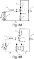
- Fig. 3A illustrates a conventional transistor circuit with source degeneration.
- the device of Fig. 3A comprises voltage source 10, transistor 13 and load 14.
- a gate inductor 31 is coupled to the gate terminal of transistor 13 having an inductance value L Gmatch for gate side impedance matching
- a drain inductor 32 is coupled to the drain terminal of transistor 13 having an inductance L Dmatch for drain side impedance matching.
- the transistor circuit of Fig. 3A comprises a source inductor L S, DEG , which provides source degeneration.
- the source terminal of transistor 13 may be floating.
- Fig. 3B illustrates a modification of the transistor circuit of Fig. 3A .
- Inductor 33A is provided in a "loop" between source and gate terminals of transistor 13, together with voltage source 10 and gate inductor 31, and inductor 33B is coupled in a "loop” between source and drain terminals of transistor 13 together with load 14 and inductor 32.
- This separation or source inductor 33 into inductors 33A and 33B separates the source current I S in Fig. 3A into the gate current (I G ) flowing through inductor 33A and the drain current I D flowing through inductor 33.
- inductors 33A, 33B may then be “moved” to a different position in the respective “loop", namely towards the gate terminal of transistor 13 in case of inductor 33A and towards the drain terminal of transistor 13 in case of inductor 33B, to thus arrive at the embodiment shown in Fig. 2 .
- a source degeneration effect similar to the effect provided by inductor 33 of Fig. 3A may be obtained.
- Fig. 4 illustrates a transistor circuit according to a further embodiment.
- the transistor circuit of Fig. 4 is based on the transistor circuit of Fig. 1 . Similar modifications as now described for Fig. 4 with respect to Fig. 1 may also be provided to other embodiments, for example the embodiment of Fig. 2 .
- DC biasing using a DC gate voltage V G and a DC drain voltage V D is used.
- Voltage V G is provided to gate inductor 11 via a resistor 41
- voltage V D is provided to drain inductor 12 via an inductor 42.
- Resistor 41 may have a resistance value R DC, G of between 50kOhm and 200kOhm, for example about 100kOhm
- inductor 42 may have an inductance value L D, D of between 5nH and 20nH, for example about 10nH.
- R DC resistance value
- L D inductance value
- DC decoupling capacitors 40 on the gate side and 43 on the drain side are provided to decouple DC voltages V G and V D from some circuit parts.
- Capacitor 40 is provided between voltage source 10 and resistor 41 as shown, and capacitor 43 is provided between inductor 42 and load 14, as shown in Fig. 4 .
- a transistor circuit as shown in Fig. 4 may for example be used in low noise amplifier.
- FIG. 5 illustrates the circuit schematic used for simulation.
- Transistor 52 in Fig. 5 corresponds to transistor 13
- inductor 50 corresponds to inductor 11
- inductor 51 corresponds to inductor 12.
- Capacitors 53, 54 correspond to capacitors 40, 43 of Fig. 4 , respectively.
- Drain side DC biasing is done via an inductor 55 corresponding to inductor 42
- gate side biasing is done via a circuit part 56, which includes circuitry comprising a current source and a diode-connected transistor to generate DC gate voltage V G .
- a similar circuit based on the conventional source degeneration using a source inductor as shown in Fig. 3 has been simulated.
- inductor 50 had an inductance of 500 pH and inductor 51 had an inductance of 400 pH.
- a coupling constant k between inductors 50 and 51 was 0.35.
- a source inductor of 250 pH was used.
- the simulation was done for a 28 nm technology at a frequency of 28 GHz, which is for example a typical frequency for 5G mobile communications applications.
- the quality factors used for the inductors in the simulation were set to 12, which is a typical number achievable at these frequencies. Both simulated circuits were tuned to have the same input matching.
- transformers may be used instead of using capacitors like capacitors 40 and 41 of Fig. 4 for DC decoupling.
- Example transistor circuits according to such embodiments are shown in Figs. 6 to 8 .
- both capacitors 40, 43 are replaced by transformers.
- gate inductor 11 coupled to the gate terminal of transistor 13 and drain inductor 12 coupled to the drain terminal of transistor 13 are provided to obtain a source degeneration effect.
- Inductor 11 is biased by DC voltage V G
- inductor 12 is biased by DC voltage V D .
- An inductor 60 forms an input coupling transformer together with gate inductor 11 to provide DC decoupling.
- the coupling constant between inductors 60 and 11 may be designed to be higher than the coupling constant k between inductors 11, 12.
- the coupling constant between inductors 60 and 11 may approximate 1, e.g. be between 0.6 and 0.9. In other embodiments, other values may be used.
- Inductor 60 is coupled to voltage source 10 as shown. Through the inductive coupling between inductors 60 and 11, the (AC) voltage generated by voltage source 10 is coupled to the gate terminal of transistor 13.
- an inductor 61 is provided coupled inductively with drain inductor 12 to form a transformer to provide DC decoupling.
- the coupling strength between inductors 12, 61 may be higher than the coupling strength between inductors 11, 12.
- the coupling strength between inductor 60 and 11 and/or the coupling strength between inductor 12 and inductor 61 may be close to 1.
- Inductor 61 is coupled to load 14.
- Through inductors 12, 61 an AC signal component of the drain current is coupled to load 14.
- the combination of inductors 60, 11, 12 and 61 may also be referred to as "quadfilar transformer".
- both capacitors 40, 43 of Fig. 4 have been replaced by transformers.
- only one of the capacitors is replaced by a transformer.
- Fig. 7 shows a transistor circuit according to an embodiment where capacitor 40 of Fig. 4 together with the biasing via resistor 41 remains, while capacitor 43 has been replaced by a transformer, which, as in Fig. 6 , is formed by drain inductor 12 and inductor 61.
- Fig. 8 shows a case where capacitor 43 and the drain side biasing via inductor 42 is implemented as in Fig. 4 , while capacitor 40 has been replaced by a transformer formed by inductor 60 and gate inductor 11, as in Fig. 6 .
- the inductors of Figs. 7 and 8 each may be regarded as forming a trifilar transformer.
- Fig. 9 essentially corresponds to the embodiment of Fig. 2 , with a negative coupling.
- an inductor 90A for gate side impedance matching corresponding to inductor of 11A is coupled, and to the drain terminal of transistor 13 an inductor 91A for drain side for drain side impedance matching is coupled, corresponding to inductor 12A of Fig. 2 .
- a gate inductor 90B is coupled, and to the drain terminal an inductor 91B is coupled, which apart from the sign of the coupling constant correspond to inductors 11B, 12B of Fig. 2 .
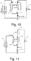
- Fig. 10 shows a transistor circuit according to a further embodiment, which apart from the negative coupling corresponds to the embodiment of Fig. 1 .
- a single gate inductor 90 coupled to the gate terminal and a single drain inductor 91 coupled to the drain terminal of transistor 13 are provided, which serve both for impedance matching and for providing the - in this case negative - coupling.
- the winding directions of inductors 90, 91 are opposite each other.
- the provision of two separate inductors at each of gate and drain terminals in Fig. 9 versus the provision of a single combined inductor for each of gate and drain terminals in Fig. 10 corresponds to the provision of separate inductors in Fig. 2 and the provision of single inductors in Fig.
- Fig. 11 shows a transistor circuit based on the embodiment of Fig. 9 , where an additional source inductor 1101 coupled to the source terminal of transistor 13 is provided.
- a transistor circuit according to an embodiment shown in Fig. 12 is based on the transistor circuit of Fig. 10 , with the additional source inductor 1101 provided.
- Source inductor 1101 in both cases causes conventional source degeneration.
- This conventional source degeneration is fully or partially counteracted by the negative source degeneration effect caused by inductors 90B, 91B of Fig. 11 or inductors 90, 91 of Fig.
- inductor 1101 may for example also be a parasitic inductor, which may be caused for example if a high line length of an electrical connection between the source terminal of transistor 13 and ground becomes necessary, which may lead to a correspondingly high inductance.
- Fig. 13 is a flow chart illustrating a method for manufacturing a transistor circuit according to an embodiment.
- the method of Fig. 13 may be used to manufacture the transistor circuits discussed with reference to Figs. 1, 2 and 4 to 12 above, but may also be used to manufacture other transistor circuits. To avoid repetitions and for ease of understanding, the method of Fig. 13 will be explained referring to the previous explanations of the transistor circuits according to various embodiments.
- Fig. 13 While the method of Fig. 13 is shown and described as a series of acts or events, the order in which these acts or events are presented is not to be construed as limiting, and the various acts or events may also be performed in different orders or also in parallel during device processing.
- the method comprises providing a field effect transistor like field effect transistor 13 of the embodiments discussed above.
- the method comprises providing an gate inductor coupled to a gate terminal of the field effect transistor, for example inductor 11, 11B, 90 or 90B of the above devices.
- the method comprises providing a drain inductor coupled to the drain terminal of the field effect transistor, for example one of inductors 12, 12B, 91 or 91B of the above embodiments.
- the inductors provided at 1302 and 1303 are provided in proximity to each other such that they exhibit a coupling, for example with an absolute value greater than 0.1 or 0.2 (positive or negative) or any of the couplings discussed above, to provide a source degeneration effect.
- the various modifications illustrated in the figures and described with respect therewith may also be implemented in the method accordingly.
- the field effect transistor at 1301 and the inductors at 1302 and 1303 may be provided on a same chip, decoupling capacitors as shown in Fig. 4 and/or transformers as shown in Figs. 6 to 8 etc. and corresponding DC biasing may be provided, etc. Therefore, it is obvious that a plurality of possible variations and modifications exist.
- Fig. 14 is a flowchart illustrating methods according to some further embodiments.
- the method of Fig. 14 may be used to operate the transistor circuits discussed with reference to Figs. 1, 2 and 4 to 12 above, but may also be used to operate other transistor circuits. To avoid repetitions and for ease of understanding, the method of Fig. 14 will be explained referring to the previous explanations of the transistor circuits according to various embodiments.
- Fig. 14 While the method of Fig. 14 is shown and described as a series of acts or events, the order in which these acts or events are presented is not to be construed as limiting, and the various acts or events may also be performed in different orders or also in parallel.
- the method comprises operating a field effect transistor, for example field effect transistor 13 of the embodiments discussed above.
- the method comprises using inductors coupled to gate and drain terminals of the field effect transistor to provide a source degeneration effect, for example as explained for inductors 11, 11B, 90 or 90B and inductors 12, 12B, 91 or 91B for the transistor circuits discussed above.
Landscapes
- Engineering & Computer Science (AREA)
- Power Engineering (AREA)
- Microelectronics & Electronic Packaging (AREA)
- Amplifiers (AREA)
- Semiconductor Integrated Circuits (AREA)
Abstract
Transistor circuits are provided including a transistor (13), a first inductor (11) coupled to the gate terminal of the transistor (13) and a second inductor (12) coupled to the drain terminal of the transistor. The first and second inductors (11, 12) are inductively coupled to provide a source degeneration effect.
Description
- The present application relates to transistor circuits and to related methods.
- Transistors are used in many electronic devices for example to switch, control or amplify voltages or currents. A frequently used transistor type is a field effect transistor like a MOSFET (metal-oxide semiconductor field effect transistor), where essentially a resistance between source and drain terminals is controlled by a gate-source voltage of the field effect transistor. Such transistors may be based on various semiconductor materials including silicon (Si), silicon carbide (SiC), gallium arsenide (GaAs) or gallium nitride (GaN).
- In radio frequency (RF) applications, such field effect transistors are used for example to implement amplifiers like low noise amplifiers (LNAs). In such RF applications, so-called source degeneration is a common approach to control the gain of the transistor or amplifier, to improve stability and/or to provide input matching and/or improve linearity. In conventional source degeneration, an element is coupled to a source terminal of a field effect transistor. In RF applications, this element is usually an inductor, whereas for low frequency applications also resistors may be used.
- This conventional source degeneration requires a floating source. However, a floating source may be undesirable in some applications or may not be available in some technologies. Moreover, sometimes it may be difficult to define and select such an inductor coupled to the source accurately, for example in cases where an inductance of a package of the device is part of the source degeneration, or when a single-ended circuit implementation is used where a ground return path of circuitry including the element coupled to the source terminal may be difficult to avoid, respectively design to a required value.
- A transistor circuit as defined in
claim 1 and a method for manufacturing a transistor device as defined inclaim 14 are provided. The dependent claims define further embodiments. - According to an embodiment, a transistor circuit is provided, comprising:
- a transistor,
- a first inductor coupled to a gate terminal of the field effect transistor, and
- a second inductor coupled to a drain terminal of the field effect transistor, wherein the first inductor and the second inductor are inductively coupled to provide a source degeneration effect for the field effect transistor.
- According to another embodiment, a method for operating a transistor circuit is provided, comprising:
- operating a transistor, and
- using a first inductor coupled to a gate terminal of the field effect transistor and a second inductor coupled to a drain terminal of the field effect transistor to provide a source degeneration effect for the field effect transistor.
- The above summary is merely intended to give a brief overview over some embodiments and is not to be construed as limiting, as other embodiments may include other features than the ones discussed above.
-
-
Fig. 1 is a circuit diagram of a transistor circuit according to an embodiment. -
Fig. 2 is a circuit diagram of a transistor circuit according to a further embodiment. -
Figs. 3A and 3B are explanatory diagrams of transistor circuits for illustrating how embodiments effect source degeneration. -
Figs. 4 to 12 are circuit diagrams of transistor circuits according to further embodiments. -
Fig. 13 is a flow chart illustrating a method according to some embodiments. -
Fig. 14 is a flow chart illustrating a method according to some further embodiments. - In the following, various embodiments will be described in detail referring to the attached drawings. These embodiments serve only illustrative purposes and are not to be construed as limiting. For example, while embodiments may be described as including a plurality of components, in other embodiments some of these components may be omitted and/or may be replaced by alternative components. In addition to the components explicitly shown and described, additional components may be provided, for example components conventionally used in transistor circuits or radio frequency (RF) circuits.
- Features or components from various embodiments may be combined to form further components. For example, in various embodiments various modifications or variations to other embodiments may be described separately. However, such modifications or variations from different embodiments and figures may also be combined unless noted otherwise.
- Connections or couplings, unless noted otherwise, apart from couplings between inductors refer to electrical connections or couplings herein. A coupling between inductors as used herein refers to an inductive (magnetic) coupling unless noted otherwise. Such connections or couplings may be modified as long as the general purpose of the connection or coupling, for example to transmit a signal, a voltage and/or a current, or to provide a coupling, is essentially maintained.
- Embodiments herein use transistors, in particular field effect transistors like MOSFETs. Such transistors have source, drain and gate terminals. While field effect transistors are used as examples in the following, techniques discussed herein may be applied to various types of transistors, including various type of field effect transistors like MOSFETs (metal oxide semiconductor field effect transistors), JFETs (junction field effect transistors) or HEMTs (high electron mobility transistors), but also other transistors like BJTs (bipolar junction transistors) or IGBTs (insulated gate bipolar transistors). As used herein, the term "gate" also includes the base of transistors like BJTs, the term "source" also includes the emitter of transistors like BJTs and IGBTs, and the term "drain" also includes the collector of transistors like BJTs and IGBTs. For example, the term "source degeneration" also includes an "emitter degeneration" for transistors having an emitter terminal.
- Transistors as used herein may be based on various semiconductor materials, for example group IV materials like silicon, group IV compounds like silicon carbide (SiC), or III-V compounds like gallium arsenide (GaAS)or gallium nitride (GaN).
- Some embodiments may be used in radio frequency (RF) applications. Radio frequency may refer to frequencies above 100 kHz, for example in the Megahertz or even Gigahertz range. For example, in some communication applications radio frequency may refer to signals having a frequency of above 1 GHz or above 10GHz.
- In some embodiments, a source degeneration effect is achieved without providing an inductor or resistor to a source terminal of a transistor. In this respect, unless noted otherwise, inductors, resistors and other elements refer to elements specifically provided to generate an inductance, a resistance etc. which is above the inductance or resistance generated by usual electrical connections like wires or leads. In other words, simple electrical connections (which always have some amount of resistance and inductance) are not regarded as inductors or resistances in this context. For example, inductors used herein may have an inductance of at least 50 pH (Picohenry), for example more than 100pH or more than 200pH. A source degeneration effect in the sense herein is an effect which causes the transistor to behave similar to a conventional source degeneration, for example as with an inductor in the above sense coupled to the source terminal, or according to a "negative" source degeneration explained further below where the transistor behaves as if a negative inductance were coupled to its source terminal.
- In the Figures, in order to avoid repetitions, like elements are designated with the same reference numerals and will not be described repeatedly. Instead, reference will be made to the description of previous figures.
-
Fig. 1 is a circuit diagram illustrating a transistor circuit according to an embodiment. The transistor circuit ofFig. 1 comprises afield effect transistor 13, having a source terminal, a drain terminal and a gate terminal.Transistor 13 may for example be used in a radio frequency circuit like a low noise amplifier (LNA), but is not limited thereto. In some embodiments,field effect transistor 13 may be a MOSFET transistor. In some radio frequency applications,transistor 13 may be based on a wide bandgap semiconductor material like gallium nitride. In other embodiments, other semiconductor materials like silicon may be used. -
Transistor 13 is controlled by avoltage source 10 having an impedance ZSOURCE and being coupled between the gate and source terminals oftransistor 13 and therefore applying a gate-source voltage. Using the gate-source voltage, essentially a drain-source resistance and current oftransistor 13 may be controlled. In some embodiments, also an operating point oftransistor 13 may be set by DC biasing. The voltage generated byvoltage source 10 may for example represent an RF signal to be amplified by a low noise amplifier. - A
gate inductor 11 is coupled to the gate terminal oftransistor 13 betweenvoltage source 10 andtransistor 13. Moreover, adrain inductor 12 is coupled to the drain terminal oftransistor 13. A dot at theinductors Fig. 1 ,inductors - Furthermore,
transistor 13 has aload 14 coupled between its drain and source terminals. The coupling ofload 14 is merely an example, and various loads may be coupled in various manners totransistor 13. - It should be noted that in the embodiment of
Fig. 1 , no inductor or relevant parasitic inductance is present between the source terminal oftransistor 13 and ground. For example, the source terminal oftransistor 13 may be coupled to ground by a simple electrical connection like a lead or a wire. Nevertheless, as will be explained further below with reference toFigs. 2 ,3A and 3B in more details,inductors transistor 13 essentially behaves as if a source degeneration inductor were connected between its source terminal and ground. However, in the embodiment ofFig. 1 , in contrast to conventional source degeneration, no floating source terminal and no specific source inductor is required. - Inductance values of
inductors Fig. 1 , the inductance ofgate inductor 11 is represented as a sum of a component inductance LSD, DEG which serves for the coupling to draininductor 12 for source degeneration and a component LG which serves for gate side (input side) impedance matching. Likewise, an inductance ofinductor 12 is represented as a sum of a component LSD, DEG for source degeneration and a component LD for drain side (output side) impedance matching. In this way, in someembodiments inductors - Due to the same winding direction, as mentioned, the coupling constant k is greater than 0. In some implementations,
inductor 11 may have an inductance greater than 100 pH, for example greater than 200 pH or 300 pH.Drain inductor 12 may also have an inductance greater than 100 pH, for example greater than 200 pH or 300 pH. Coupling constant k may be at least 0.1, for example 0.2 or more, for example between 0.3 and 0.5, and may approach a coupling constant k=1. - To provide a high coupling constant,
inductors transistor 13 may be integrated on a same chip, which chip is indicated byreference numeral 15 inFig. 1 . Further components may also be provided on this chip. By an integration on the same chip,inductors - In
Fig. 1 , IG denotes a gate current and ID denotes a drain current. A source current IS is the sum of gate current IG and drain current ID. Voltage source 10,load 14 and the source terminal oftransistor 13 are coupled to a common ground, and no floating source terminal is necessary. - In
Fig. 1 , additionally a DC biasing on gate and drain side oftransistor 13 may be provided, which will be explained later with respect toFig. 4 , but is omitted inFigs. 1 and 2 . - While in
Fig. 1 inductors for impedance matching and for providing the coupling to provide a source degeneration effect are combined ininductors Fig. 2 . InFig. 2 ,inductor 11 is split into afirst inductor 11A having an inductivity LG Match for gate side impedance matching and aninductor 11B having an inductivity LSG, DEG for providing the source degeneration effect.Inductor 12 ofFig. 1 is replaced by afirst inductor 12A having an inductivity LD Match for drain side impedance matching and aninductor 12B having an inductivity LSD, DEG for providing the source degeneration effect.Inductors inductors Fig. 1 ,inductors Fig. 1 . In an ideal case, the coupling constant k may approach or be equal to 1, as shown inFig. 2 . - This ideal case of k=1 will now be used to explain how by providing gate and drain inductors with an appropriate coupling a source degeneration effect may be achieved. For this explanation, reference is additionally made to
Figs. 3A and 3B . -
Fig. 3A illustrates a conventional transistor circuit with source degeneration. As inFig. 1 and 2 , the device ofFig. 3A comprisesvoltage source 10,transistor 13 andload 14. Agate inductor 31 is coupled to the gate terminal oftransistor 13 having an inductance value LGmatch for gate side impedance matching, and adrain inductor 32 is coupled to the drain terminal oftransistor 13 having an inductance LDmatch for drain side impedance matching. - Furthermore, the transistor circuit of
Fig. 3A comprises a source inductor LS, DEG, which provides source degeneration. To provide source degeneration, the source terminal oftransistor 13 may be floating. -
Fig. 3B illustrates a modification of the transistor circuit ofFig. 3A . Here,source inductor 33 is replaced by two perfectly coupled (k=1)source degeneration inductors Inductor 33A is provided in a "loop" between source and gate terminals oftransistor 13, together withvoltage source 10 andgate inductor 31, andinductor 33B is coupled in a "loop" between source and drain terminals oftransistor 13 together withload 14 andinductor 32. This separation orsource inductor 33 intoinductors Fig. 3A into the gate current (IG) flowing throughinductor 33A and the drain current ID flowing throughinductor 33. - These
inductors transistor 13 in case ofinductor 33A and towards the drain terminal oftransistor 13 in case ofinductor 33B, to thus arrive at the embodiment shown inFig. 2 . Based on this, it can be easily understood that by providing inductively coupled gate and drain inductors as inFigs. 1 and 2 , a source degeneration effect similar to the effect provided byinductor 33 ofFig. 3A may be obtained. -
Fig. 4 illustrates a transistor circuit according to a further embodiment. The transistor circuit ofFig. 4 is based on the transistor circuit ofFig. 1 . Similar modifications as now described forFig. 4 with respect toFig. 1 may also be provided to other embodiments, for example the embodiment ofFig. 2 . - In particular, in the embodiment of
Fig. 4 , DC biasing using a DC gate voltage VG and a DC drain voltage VD is used. Voltage VG is provided togate inductor 11 via aresistor 41, and voltage VD is provided to draininductor 12 via aninductor 42.Resistor 41 may have a resistance value RDC, G of between 50kOhm and 200kOhm, for example about 100kOhm, andinductor 42 may have an inductance value LD, D of between 5nH and 20nH, for example about 10nH. However, these values are merely examples, and other values may be used depending on the implementation. Furthermore,DC decoupling capacitors 40 on the gate side and 43 on the drain side are provided to decouple DC voltages VG and VD from some circuit parts.Capacitor 40 is provided betweenvoltage source 10 andresistor 41 as shown, andcapacitor 43 is provided betweeninductor 42 andload 14, as shown inFig. 4 . A transistor circuit as shown inFig. 4 may for example be used in low noise amplifier. - A circuit based on the transistor circuit of
Fig. 4 has been simulated and compared with a conventional device.Fig. 5 illustrates the circuit schematic used for simulation.Transistor 52 inFig. 5 corresponds totransistor 13,inductor 50 corresponds to inductor 11,inductor 51 corresponds toinductor 12.Capacitors capacitors Fig. 4 , respectively. Drain side DC biasing is done via aninductor 55 corresponding toinductor 42, and gate side biasing is done via acircuit part 56, which includes circuitry comprising a current source and a diode-connected transistor to generate DC gate voltage VG. For comparison, a similar circuit based on the conventional source degeneration using a source inductor as shown inFig. 3 has been simulated. - For the simulation of the circuit of
Fig. 5 ,inductor 50 had an inductance of 500 pH andinductor 51 had an inductance of 400 pH. A coupling constant k betweeninductors Fig. 3 , a source inductor of 250 pH was used. - The simulation was done for a 28 nm technology at a frequency of 28 GHz, which is for example a typical frequency for 5G mobile communications applications. The quality factors used for the inductors in the simulation were set to 12, which is a typical number achievable at these frequencies. Both simulated circuits were tuned to have the same input matching.
- According to the simulation results, the same input matching may be obtained, but in
Fig. 5 no additional inductor for input matching needs to be provided. Noise was improved compared to the conventional approach, and there was also an improvement in the gain attributed to a bulk connection oftransistor 52. Furthermore, effective losses were decreased to some extent through the use of two separate inductors with the same Q constants instead of inductor for source degeneration. - Instead of using capacitors like
capacitors Fig. 4 for DC decoupling, in other embodiments transformers may be used. Example transistor circuits according to such embodiments are shown inFigs. 6 to 8 . InFig. 6 , bothcapacitors Fig. 1 gate inductor 11 coupled to the gate terminal oftransistor 13 anddrain inductor 12 coupled to the drain terminal oftransistor 13 are provided to obtain a source degeneration effect.Inductor 11 is biased by DC voltage VG, andinductor 12 is biased by DC voltage VD. - An
inductor 60 forms an input coupling transformer together withgate inductor 11 to provide DC decoupling. The coupling constant betweeninductors inductors inductors Inductor 60 is coupled tovoltage source 10 as shown. Through the inductive coupling betweeninductors voltage source 10 is coupled to the gate terminal oftransistor 13. - Furthermore, instead of
capacitor 43, aninductor 61 is provided coupled inductively withdrain inductor 12 to form a transformer to provide DC decoupling. The coupling strength betweeninductors inductors inductor inductor 12 andinductor 61 may be close to 1.Inductor 61 is coupled to load 14. Throughinductors inductors - In
Fig. 6 , bothcapacitors Fig. 4 have been replaced by transformers. In other embodiments now discussed with reference toFigs. 7 and8 , only one of the capacitors is replaced by a transformer. - For example,
Fig. 7 shows a transistor circuit according to an embodiment wherecapacitor 40 ofFig. 4 together with the biasing viaresistor 41 remains, whilecapacitor 43 has been replaced by a transformer, which, as inFig. 6 , is formed bydrain inductor 12 andinductor 61. -
Fig. 8 shows a case wherecapacitor 43 and the drain side biasing viainductor 42 is implemented as inFig. 4 , whilecapacitor 40 has been replaced by a transformer formed byinductor 60 andgate inductor 11, as inFig. 6 . The inductors ofFigs. 7 and8 each may be regarded as forming a trifilar transformer. - In the embodiments thus discussed so far, a positive coupling between
inductors transistor 13, respectively, was used to provide a source degeneration effect, which corresponds to the conventional source degeneration effect. By using two inductors coupled to gate and drain terminals instead of an inductor coupled to the source terminal as in conventional solutions, instead of a positive coupling (k>0) also a negative coupling may be introduced. This, in effect, corresponds to coupling a "negative inductance" to the source terminal of the transistor and therefore leads to a "negative" source degeneration effect. This in some implementations may be used to increase the gain or may be used to compensate an unwanted source degeneration. This "negative" source degeneration effect is also a source degeneration effect in the sense used herein. Corresponding embodiments will now be discussed referring toFigs. 9 to 12 . - The embodiment of
Fig. 9 essentially corresponds to the embodiment ofFig. 2 , with a negative coupling. To the gate terminal oftransistor 13, aninductor 90A for gate side impedance matching corresponding to inductor of 11A is coupled, and to the drain terminal oftransistor 13 aninductor 91A for drain side for drain side impedance matching is coupled, corresponding toinductor 12A ofFig. 2 . - Moreover, to the gate terminal a
gate inductor 90B is coupled, and to the drain terminal aninductor 91B is coupled, which apart from the sign of the coupling constant correspond toinductors Fig. 2 . As seen by the dots inFig. 9 , in contrast toinductors 12B inductors Fig. 9 have opposite winding directions. This leads to a coupling constant k<0, which in an ideal case may be a coupling constant k=-1. -
Fig. 10 shows a transistor circuit according to a further embodiment, which apart from the negative coupling corresponds to the embodiment ofFig. 1 . Here, asingle gate inductor 90 coupled to the gate terminal and asingle drain inductor 91 coupled to the drain terminal oftransistor 13 are provided, which serve both for impedance matching and for providing the - in this case negative - coupling. Again, the winding directions ofinductors Fig. 9 versus the provision of a single combined inductor for each of gate and drain terminals inFig. 10 corresponds to the provision of separate inductors inFig. 2 and the provision of single inductors inFig. 1 for the case of a positive coupling. All explanations regarding inductances, magnitude of the coupling constants etc. made for the embodiments ofFig. 1 and 2 , with the exception of the opposite winding directions and therefore opposite signs of the coupling constants, and the provision on a single chip are also applicable to the embodiments ofFigs. 9 and10 . In other words, for example the absolute values of the coupling constants may be the same as explained for the embodiments ofFigs. 1 and 2 . Moreover, also DC biasing like explained with reference toFigs. 4 ,6 ,7 and8 may be provided in the embodiments ofFig. 9 and10 . - As briefly mentioned above, such a "negative" source degeneration effect may be used to compensate an unwanted source degeneration. This will be further explained referring to
Figs. 11 and12 .Fig. 11 shows a transistor circuit based on the embodiment ofFig. 9 , where anadditional source inductor 1101 coupled to the source terminal oftransistor 13 is provided. In a similar manner, a transistor circuit according to an embodiment shown inFig. 12 is based on the transistor circuit ofFig. 10 , with theadditional source inductor 1101 provided.Source inductor 1101 in both cases causes conventional source degeneration. This conventional source degeneration is fully or partially counteracted by the negative source degeneration effect caused byinductors Fig. 11 orinductors Fig. 12 . Such an approach may be of interest in cases where an unwanted source degeneration or a too high source degeneration is present e.g. due to layout/implementation restrictions that make the provision ofinductor 1101 unavoidable or highly desirable. In such cases,inductor 1101 may for example also be a parasitic inductor, which may be caused for example if a high line length of an electrical connection between the source terminal oftransistor 13 and ground becomes necessary, which may lead to a correspondingly high inductance. - However, the compensation of a conventional source degeneration of
Figs. 11 and12 is only one application for using the negative source degeneration effect explained above. -
Fig. 13 is a flow chart illustrating a method for manufacturing a transistor circuit according to an embodiment. The method ofFig. 13 may be used to manufacture the transistor circuits discussed with reference toFigs. 1, 2 and4 to 12 above, but may also be used to manufacture other transistor circuits. To avoid repetitions and for ease of understanding, the method ofFig. 13 will be explained referring to the previous explanations of the transistor circuits according to various embodiments. - While the method of
Fig. 13 is shown and described as a series of acts or events, the order in which these acts or events are presented is not to be construed as limiting, and the various acts or events may also be performed in different orders or also in parallel during device processing. - At 1301, the method comprises providing a field effect transistor like
field effect transistor 13 of the embodiments discussed above. At 1302, the method comprises providing an gate inductor coupled to a gate terminal of the field effect transistor, forexample inductor inductors - The inductors provided at 1302 and 1303 are provided in proximity to each other such that they exhibit a coupling, for example with an absolute value greater than 0.1 or 0.2 (positive or negative) or any of the couplings discussed above, to provide a source degeneration effect. The various modifications illustrated in the figures and described with respect therewith may also be implemented in the method accordingly. For example, the field effect transistor at 1301 and the inductors at 1302 and 1303 may be provided on a same chip, decoupling capacitors as shown in
Fig. 4 and/or transformers as shown inFigs. 6 to 8 etc. and corresponding DC biasing may be provided, etc. Therefore, it is obvious that a plurality of possible variations and modifications exist. -
Fig. 14 is a flowchart illustrating methods according to some further embodiments. - The method of
Fig. 14 may be used to operate the transistor circuits discussed with reference toFigs. 1, 2 and4 to 12 above, but may also be used to operate other transistor circuits. To avoid repetitions and for ease of understanding, the method ofFig. 14 will be explained referring to the previous explanations of the transistor circuits according to various embodiments. - While the method of
Fig. 14 is shown and described as a series of acts or events, the order in which these acts or events are presented is not to be construed as limiting, and the various acts or events may also be performed in different orders or also in parallel. - At 1401, the method comprises operating a field effect transistor, for example
field effect transistor 13 of the embodiments discussed above. - At 1402, the method comprises using inductors coupled to gate and drain terminals of the field effect transistor to provide a source degeneration effect, for example as explained for
inductors inductors - Some embodiments are defined by the following examples:
- Example 1. A transistor circuit, comprising:
- a transistor,
- a first inductor coupled to the gate terminal of the transistor, and
- a second inductor coupled to the drain terminal of the transistor, wherein the first inductor and the second inductor are inductively coupled to provide a source degeneration effect for the transistor.
- Example 2. The transistor circuit of example 1, wherein an absolute coupling strength between the first inductor and the second inductor is greater than 0.1.
- Example 3. The transistor circuit of example 2, wherein the absolute coupling strength is greater than 0.2.
- Example 4. The transistor circuit of any one of examples 1 to 3, wherein the transistor (13, 52), the first inductor and the second inductor are integrated on a same chip.
- Example 5. The transistor circuit of any one of examples 1 to 4, wherein the coupling is positive.
- Example 6. The transistor circuit of any one of examples 1 to 4, wherein the coupling is negative.
- Example 7. The transistor circuit of example 6, further comprising a third inductor coupled to a source terminal of the transistor, wherein the negative coupling at least partially compensates a source degeneration effect by the third inductor.
- Example 8. The transistor circuit of any one of examples 1 to 7, wherein the first inductor is dimensioned to provide gate side impedance matching.
- Example 9. The transistor circuit of any one of examples 1 to 8, further comprising a first compensation circuitry coupled to the gate terminal and dimensioned to provide gate side impedance matching.
- Example 10. The transistor circuit of any one of examples 1 to 9, wherein the second inductor is dimensioned to provide drain side impedance matching.
- Examples 11. The transistor circuit of any one of examples 1 to 9, further comprising a second compensation circuitry coupled to the drain terminal and dimensioned to provide drain side impedance matching.
- Example 12. The transistor circuit of any one of examples 1 to 11, further comprising a capacitor coupled to the first inductor to provide DC decoupling.
- Example 13. The transistor circuit of any one of examples 1 to 11, further comprising a fourth inductor inductively coupled to the first inductor to provide DC decoupling.
- Example 14. The transistor circuit of any one of examples 1 to 13, further comprising a capacitor coupled to the second inductor to provide DC decoupling.
- Example 15. The transistor circuit of any one of examples 1 to 13, further comprising a fifth inductor inductively coupled to the second inductor to provide DC decoupling.
- Example 16. A low noise amplifier, comprising the transistor circuit of any one of examples 1 to 15.
- Example 17. A method for providing a transistor circuit, comprising:
- providing a transistor,
- providing a first inductor coupled to a gate terminal of the transistor,
- providing a second inductor coupled to the drain terminal of the transistor,
- wherein the first inductor and the second inductor are arranged to be inductively coupled to provide a source degeneration effect.
- Example 18. The method of example 17, wherein the method is configured to manufacture the transistor circuit of any one of examples 1 to 15.
- Example 19. A method for operating a transistor circuit, comprising:
- operating a transistor, and
- using a first inductor coupled to a gate terminal of the transistor and a second inductor coupled to a drain terminal of the transistor to provide a source degeneration effect for the transistor.
- Example 20. The method of example 19, wherein the method is used to operate the transistor circuit of any one of examples 1 to 15.
- Although specific embodiments have been illustrated and described herein, it will be appreciated by those of ordinary skill in the art that a variety of alternate and/or equivalent implementations may be substituted for the specific embodiments shown and described without departing from the scope of the present invention. This application is intended to cover any adaptations or variations of the specific embodiments discussed herein. Therefore, it is intended that this invention be limited only by the claims and the equivalents thereof.
Claims (15)
- A transistor circuit, comprising:a transistor (13, 52),a first inductor (11; 11B; 90; 90B; 50) coupled to the gate terminal of the transistor (13), anda second inductor (12; 12B; 91; 91B; 51) coupled to the drain terminal of the transistor (13), wherein the first inductor (11; 11B; 90; 90B; 50) and the second inductor (12; 12B; 91; 91B; 51) are inductively coupled to provide a source degeneration effect for the transistor (13, 52).
- The transistor circuit of claim 1, wherein an absolute coupling strength between the first inductor (11; 11B; 90; 90B; 50) and the second inductor (12; 12B; 91; 91B; 51) is greater than 0.1.
- The transistor circuit of claim 1 or 2, wherein the transistor (13, 52), the first inductor (11; 11B; 90; 90B; 50) and the second inductor (12; 12B; 91; 91B; 51) are integrated on a same chip (15).
- The transistor circuit of any one of claims 1 to 3, wherein the coupling is positive.
- The transistor circuit of any one of claims 1 to 3, wherein the coupling is negative.
- The transistor circuit of claim 5, further comprising a third inductor (1101) coupled to a source terminal of the transistor (13, 52), wherein the negative coupling at least partially compensates a source degeneration effect by the third inductor.
- The transistor circuit of any one of claims 1 to 6, wherein the first inductor (11, 90) is dimensioned to provide gate side impedance matching.
- The transistor circuit of any one of claims 1 to 7, further comprising first compensation circuitry (11A; 90A) coupled to the gate terminal and dimensioned to provide gate side impedance matching.
- The transistor circuit of any one of claims 1 to 8, wherein the second inductor (12; 91) is dimensioned to provide drain side impedance matching.
- The transistor circuit of any one of claims 1 to 8, further comprising a second compensation circuitry (12A; 91A) coupled to the drain terminal and dimensioned to provide drain side impedance matching.
- The transistor circuit of any one of claims 1 to 10, further comprising one of a capacitor (40) coupled to the first inductor (11; 11B; 90; 90B; 50) to provide DC decoupling, or a fourth inductor (60) inductively coupled to the first inductor (11; 11B; 90; 90B; 50) to provide DC decoupling.
- The transistor circuit of any one of claims 1 to 11, further comprising one of a capacitor (43) coupled to the second inductor (12; 12B; 91; 91B; 51) to provide DC decoupling, or a fifth inductor (61) inductively coupled to the second inductor (12; 12B; 91; 91B; 51) to provide DC decoupling.
- A low noise amplifier, comprising the transistor circuit of any one of claims 1 to 12.
- A method for operating a transistor circuit, comprising:operating a transistor (13, 52), andusing a first inductor (11; 11B; 90; 90B; 50) coupled to a gate terminal of the transistor (13, 52) and a second inductor (12; 12B; 91; 91B; 51) coupled to a drain terminal of the transistor (13, 52) to provide a source degeneration effect for the transistor.
- The method of claim 14, wherein the method is used to operate the transistor circuit of any one of claims 1 to 12.
Priority Applications (1)
| Application Number | Priority Date | Filing Date | Title |
|---|---|---|---|
| EP19190431.7A EP3772820A1 (en) | 2019-08-07 | 2019-08-07 | Transistor circuits and methods for source degeneration |
Applications Claiming Priority (1)
| Application Number | Priority Date | Filing Date | Title |
|---|---|---|---|
| EP19190431.7A EP3772820A1 (en) | 2019-08-07 | 2019-08-07 | Transistor circuits and methods for source degeneration |
Publications (1)
| Publication Number | Publication Date |
|---|---|
| EP3772820A1 true EP3772820A1 (en) | 2021-02-10 |
Family
ID=67551237
Family Applications (1)
| Application Number | Title | Priority Date | Filing Date |
|---|---|---|---|
| EP19190431.7A Withdrawn EP3772820A1 (en) | 2019-08-07 | 2019-08-07 | Transistor circuits and methods for source degeneration |
Country Status (1)
| Country | Link |
|---|---|
| EP (1) | EP3772820A1 (en) |
Cited By (1)
| Publication number | Priority date | Publication date | Assignee | Title |
|---|---|---|---|---|
| CN116015221A (en) * | 2023-03-24 | 2023-04-25 | 安徽矽磊电子科技有限公司 | Radio frequency amplifier circuit based on negative feedback of transformer |
Citations (3)
| Publication number | Priority date | Publication date | Assignee | Title |
|---|---|---|---|---|
| WO2004086608A1 (en) * | 2003-03-28 | 2004-10-07 | Koninklijke Philips Electronics N.V. | Neutralization of feedback capacitance in amplifiers |
| US20120218041A1 (en) * | 2011-02-24 | 2012-08-30 | Fujitsu Limited | Amplifier circuit |
| US20140191800A1 (en) * | 2013-01-07 | 2014-07-10 | Analog Devices, Inc. | Multiple winding transformer coupled amplifier |
-
2019
- 2019-08-07 EP EP19190431.7A patent/EP3772820A1/en not_active Withdrawn
Patent Citations (3)
| Publication number | Priority date | Publication date | Assignee | Title |
|---|---|---|---|---|
| WO2004086608A1 (en) * | 2003-03-28 | 2004-10-07 | Koninklijke Philips Electronics N.V. | Neutralization of feedback capacitance in amplifiers |
| US20120218041A1 (en) * | 2011-02-24 | 2012-08-30 | Fujitsu Limited | Amplifier circuit |
| US20140191800A1 (en) * | 2013-01-07 | 2014-07-10 | Analog Devices, Inc. | Multiple winding transformer coupled amplifier |
Cited By (2)
| Publication number | Priority date | Publication date | Assignee | Title |
|---|---|---|---|---|
| CN116015221A (en) * | 2023-03-24 | 2023-04-25 | 安徽矽磊电子科技有限公司 | Radio frequency amplifier circuit based on negative feedback of transformer |
| CN116015221B (en) * | 2023-03-24 | 2023-05-26 | 安徽矽磊电子科技有限公司 | Radio frequency amplifier circuit based on negative feedback of transformer |
Similar Documents
| Publication | Publication Date | Title |
|---|---|---|
| US8970308B2 (en) | Input match network with RF bypass path | |
| US5486787A (en) | Monolithic microwave integrated circuit apparatus | |
| KR101697398B1 (en) | An input match network for a power circuit | |
| EP3662577B1 (en) | Broadband harmonic matching network | |
| CN110021583B (en) | Compensation devices for transistors | |
| US9118367B2 (en) | Wideband power efficient high transmission power radio frequency (RF) transmitter | |
| US20140022021A1 (en) | Power amplifier | |
| JP2008533899A (en) | RF transistor output matching method and system | |
| US10784825B2 (en) | RF power amplifier with frequency selective impedance matching network | |
| KR20200091867A (en) | RF power amplifier with combined baseband, fundamental and harmonic tuning network | |
| US20180167038A1 (en) | Fully depleted silicon on insulator power amplifier | |
| CN111884610B (en) | Microwave amplifiers resistant to electrical overstress | |
| US12212289B2 (en) | Group III nitride based depletion mode differential amplifiers and related RF transistor amplifier circuits | |
| CN109818580B (en) | Power amplifier and compound semiconductor device | |
| JP3130809B2 (en) | Semiconductor device | |
| US12068721B2 (en) | Monolithic microwave integrated circuits tolerant to electrical overstress | |
| US12028023B2 (en) | Amplifier | |
| JP7718120B2 (en) | Amplification circuit | |
| US9531334B1 (en) | Broadband circuit for an active device | |
| US20050104664A1 (en) | Intergrated power amplifier arrangement | |
| US12537486B2 (en) | Amplifier with output harmonic termination and output impedance network |
Legal Events
| Date | Code | Title | Description |
|---|---|---|---|
| PUAI | Public reference made under article 153(3) epc to a published international application that has entered the european phase |
Free format text: ORIGINAL CODE: 0009012 |
|
| STAA | Information on the status of an ep patent application or granted ep patent |
Free format text: STATUS: THE APPLICATION HAS BEEN PUBLISHED |
|
| AK | Designated contracting states |
Kind code of ref document: A1 Designated state(s): AL AT BE BG CH CY CZ DE DK EE ES FI FR GB GR HR HU IE IS IT LI LT LU LV MC MK MT NL NO PL PT RO RS SE SI SK SM TR |
|
| AX | Request for extension of the european patent |
Extension state: BA ME |
|
| STAA | Information on the status of an ep patent application or granted ep patent |
Free format text: STATUS: THE APPLICATION IS DEEMED TO BE WITHDRAWN |
|
| 18D | Application deemed to be withdrawn |
Effective date: 20210811 |