EP3772751B1 - Display module, display panel, and display apparatus - Google Patents
Display module, display panel, and display apparatus Download PDFInfo
- Publication number
- EP3772751B1 EP3772751B1 EP20180008.3A EP20180008A EP3772751B1 EP 3772751 B1 EP3772751 B1 EP 3772751B1 EP 20180008 A EP20180008 A EP 20180008A EP 3772751 B1 EP3772751 B1 EP 3772751B1
- Authority
- EP
- European Patent Office
- Prior art keywords
- display
- panel
- module
- frame
- boss
- Prior art date
- Legal status (The legal status is an assumption and is not a legal conclusion. Google has not performed a legal analysis and makes no representation as to the accuracy of the status listed.)
- Active
Links
Images




Classifications
-
- H—ELECTRICITY
- H10—SEMICONDUCTOR DEVICES; ELECTRIC SOLID-STATE DEVICES NOT OTHERWISE PROVIDED FOR
- H10H—INORGANIC LIGHT-EMITTING SEMICONDUCTOR DEVICES HAVING POTENTIAL BARRIERS
- H10H20/00—Individual inorganic light-emitting semiconductor devices having potential barriers, e.g. light-emitting diodes [LED]
- H10H20/80—Constructional details
- H10H20/81—Bodies
- H10H20/813—Bodies having a plurality of light-emitting regions, e.g. multi-junction LEDs or light-emitting devices having photoluminescent regions within the bodies
-
- G—PHYSICS
- G09—EDUCATION; CRYPTOGRAPHY; DISPLAY; ADVERTISING; SEALS
- G09F—DISPLAYING; ADVERTISING; SIGNS; LABELS OR NAME-PLATES; SEALS
- G09F9/00—Indicating arrangements for variable information in which the information is built-up on a support by selection or combination of individual elements
- G09F9/30—Indicating arrangements for variable information in which the information is built-up on a support by selection or combination of individual elements in which the desired character or characters are formed by combining individual elements
- G09F9/302—Indicating arrangements for variable information in which the information is built-up on a support by selection or combination of individual elements in which the desired character or characters are formed by combining individual elements characterised by the form or geometrical disposition of the individual elements
- G09F9/3026—Video wall, i.e. stackable semiconductor matrix display modules
-
- G—PHYSICS
- G09—EDUCATION; CRYPTOGRAPHY; DISPLAY; ADVERTISING; SEALS
- G09F—DISPLAYING; ADVERTISING; SIGNS; LABELS OR NAME-PLATES; SEALS
- G09F9/00—Indicating arrangements for variable information in which the information is built-up on a support by selection or combination of individual elements
- G09F9/30—Indicating arrangements for variable information in which the information is built-up on a support by selection or combination of individual elements in which the desired character or characters are formed by combining individual elements
- G09F9/33—Indicating arrangements for variable information in which the information is built-up on a support by selection or combination of individual elements in which the desired character or characters are formed by combining individual elements being semiconductor devices, e.g. diodes
-
- H—ELECTRICITY
- H05—ELECTRIC TECHNIQUES NOT OTHERWISE PROVIDED FOR
- H05K—PRINTED CIRCUITS; CASINGS OR CONSTRUCTIONAL DETAILS OF ELECTRIC APPARATUS; MANUFACTURE OF ASSEMBLAGES OF ELECTRICAL COMPONENTS
- H05K1/00—Printed circuits
- H05K1/02—Details
- H05K1/14—Structural association of two or more printed circuits
- H05K1/147—Structural association of two or more printed circuits at least one of the printed circuits being bent or folded, e.g. by using a flexible printed circuit
-
- H—ELECTRICITY
- H05—ELECTRIC TECHNIQUES NOT OTHERWISE PROVIDED FOR
- H05K—PRINTED CIRCUITS; CASINGS OR CONSTRUCTIONAL DETAILS OF ELECTRIC APPARATUS; MANUFACTURE OF ASSEMBLAGES OF ELECTRICAL COMPONENTS
- H05K1/00—Printed circuits
- H05K1/18—Printed circuits structurally associated with non-printed electric components
- H05K1/189—Printed circuits structurally associated with non-printed electric components characterised by the use of flexible or folded printed circuits
-
- H—ELECTRICITY
- H05—ELECTRIC TECHNIQUES NOT OTHERWISE PROVIDED FOR
- H05K—PRINTED CIRCUITS; CASINGS OR CONSTRUCTIONAL DETAILS OF ELECTRIC APPARATUS; MANUFACTURE OF ASSEMBLAGES OF ELECTRICAL COMPONENTS
- H05K7/00—Constructional details common to different types of electric apparatus
- H05K7/20—Modifications to facilitate cooling, ventilating, or heating
- H05K7/20954—Modifications to facilitate cooling, ventilating, or heating for display panels
-
- H—ELECTRICITY
- H10—SEMICONDUCTOR DEVICES; ELECTRIC SOLID-STATE DEVICES NOT OTHERWISE PROVIDED FOR
- H10H—INORGANIC LIGHT-EMITTING SEMICONDUCTOR DEVICES HAVING POTENTIAL BARRIERS
- H10H20/00—Individual inorganic light-emitting semiconductor devices having potential barriers, e.g. light-emitting diodes [LED]
- H10H20/80—Constructional details
- H10H20/85—Packages
- H10H20/8506—Containers
-
- H—ELECTRICITY
- H10—SEMICONDUCTOR DEVICES; ELECTRIC SOLID-STATE DEVICES NOT OTHERWISE PROVIDED FOR
- H10H—INORGANIC LIGHT-EMITTING SEMICONDUCTOR DEVICES HAVING POTENTIAL BARRIERS
- H10H20/00—Individual inorganic light-emitting semiconductor devices having potential barriers, e.g. light-emitting diodes [LED]
- H10H20/80—Constructional details
- H10H20/85—Packages
- H10H20/852—Encapsulations
-
- H—ELECTRICITY
- H10—SEMICONDUCTOR DEVICES; ELECTRIC SOLID-STATE DEVICES NOT OTHERWISE PROVIDED FOR
- H10H—INORGANIC LIGHT-EMITTING SEMICONDUCTOR DEVICES HAVING POTENTIAL BARRIERS
- H10H20/00—Individual inorganic light-emitting semiconductor devices having potential barriers, e.g. light-emitting diodes [LED]
- H10H20/80—Constructional details
- H10H20/85—Packages
- H10H20/857—Interconnections, e.g. lead-frames, bond wires or solder balls
-
- H—ELECTRICITY
- H10—SEMICONDUCTOR DEVICES; ELECTRIC SOLID-STATE DEVICES NOT OTHERWISE PROVIDED FOR
- H10H—INORGANIC LIGHT-EMITTING SEMICONDUCTOR DEVICES HAVING POTENTIAL BARRIERS
- H10H29/00—Integrated devices, or assemblies of multiple devices, comprising at least one light-emitting semiconductor element covered by group H10H20/00
- H10H29/10—Integrated devices comprising at least one light-emitting semiconductor component covered by group H10H20/00
- H10H29/14—Integrated devices comprising at least one light-emitting semiconductor component covered by group H10H20/00 comprising multiple light-emitting semiconductor components
- H10H29/142—Two-dimensional arrangements, e.g. asymmetric LED layout
-
- H—ELECTRICITY
- H05—ELECTRIC TECHNIQUES NOT OTHERWISE PROVIDED FOR
- H05K—PRINTED CIRCUITS; CASINGS OR CONSTRUCTIONAL DETAILS OF ELECTRIC APPARATUS; MANUFACTURE OF ASSEMBLAGES OF ELECTRICAL COMPONENTS
- H05K2201/00—Indexing scheme relating to printed circuits covered by H05K1/00
- H05K2201/10—Details of components or other objects attached to or integrated in a printed circuit board
- H05K2201/10007—Types of components
- H05K2201/10128—Display
-
- H—ELECTRICITY
- H10—SEMICONDUCTOR DEVICES; ELECTRIC SOLID-STATE DEVICES NOT OTHERWISE PROVIDED FOR
- H10W—GENERIC PACKAGES, INTERCONNECTIONS, CONNECTORS OR OTHER CONSTRUCTIONAL DETAILS OF DEVICES COVERED BY CLASS H10
- H10W90/00—Package configurations
Definitions
- Embodiments of the disclosure relate to a display module, a display panel, and a display apparatus, and more particularly, to a display apparatus including a display panel including a plurality of display modules formed by mounting a plurality of inorganic light emitting diodes.
- a display apparatus is a type of output device that visually displays data information, such as text or graphics, and images.
- a liquid crystal panel or an organic light emitting diode (OLED) panel that is formed by depositing an OLED on a substrate has been used for a display apparatus.
- the liquid crystal panel has difficulties such as a slow reaction time, and large power consumption.
- the liquid crystal panel has difficulties in the compact design because it does not emit light itself and thus requires a backlight.
- OLED panels have a short service life and poor production yield rates. Accordingly, as a new panel to replace the panels, a micro light emitting diode (micro LED or ⁇ LED) display panel that mounts an inorganic light emitting diode on a substrate and uses the inorganic light emitting diode itself as a pixel has been studied.
- the micro LED display panel is one of the flat panel display panels and composed of a plurality of inorganic light emitting diodes (inorganic LEDs) of 100 micrometers or less. In comparison with liquid crystal display (LCD) panels that require a backlight, the micro LED display panel provides better contrast, response time, and energy efficiency. Both organic light emitting diodes (OLEDs) and micro LEDs corresponding to inorganic light emitting diodes have good energy efficiency, but the micro LEDs have better brightness and luminous efficiency and a longer service life than the OLEDs.
- OLEDs organic light emitting diodes
- micro LEDs have good energy efficiency, but the micro LEDs have better brightness and luminous efficiency and a longer service life than the OLEDs.
- the micro LED display panel does not need a backlight and may have a minimized bezel, it is possible to implement compact and thin designs; and to have excellent brightness, resolution, power consumption, and durability.
- the micro LED display panel may be manufactured in various resolutions and sizes according to the customer's order and it is easy to implement a big screen by assembling unit panel modules.
- WO 2019/094287 discloses sub-displays with alignment structures and tiled displays fabricated from the sub-displays.
- GB 2 531 558 discloses a tiled microdisplay.
- US 2017/0159876 discloses a magnetically actuated fastener.
- US2019/0179592 discloses a display apparatus with display modules.
- a plate in the disclosure includes a thin film or sheet, comprehensively.
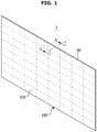
- FIG. 1 is a view illustrating an exterior of a display apparatus according to an embodiment of the disclosure.
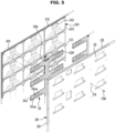
- FIG. 2 is an exploded view of main components of the display apparatus illustrated in FIG. 1 .
- FIG. 3 is a view illustrating a rear surface of one display module among the plurality of display modules illustrated in FIG. 2 .
- FIG. 4 is a view illustrating a state in which a panel board is mounted on the display panel illustrated in FIG. 2 .
- FIG. 5 is a view illustrating a state in which the panel board and a frame are mounted on the display panel illustrated in FIG. 2 .
- FIG. 6 is a view illustrating a part of a cross section along line A-A' of FIG. 1 .
- FIG. 7 is an enlarged view illustrating a part B of FIG. 6 .
- a display apparatus 1 is a device configured to display information, materials, data and the like with characters, figures, graphs, images, etc., and TV, personal computer (PC), mobile, and digital signage may be implemented with the display apparatus 1.
- the display apparatus 1 may be installed on the ground by a stand (not shown) or may be installed on the wall.
- the display apparatus 1 includes a display panel 100 on which an image is displayed, a frame 20 configured to support the display panel 100, and a rear cover 10 configured to accommodate the display panel 100 and the frame 20.
- the display panel 100 installed on the frame 20 may implement a screen of the display apparatus 1.
- the rear cover 10 forms a part of the exterior of the display apparatus 1.
- the rear cover 10 may form a rear exterior of the display apparatus 1.
- the rear cover 10 may be arranged to cover the rear of the frame 20.
- the rear cover 10 and the frame 20 may be formed of a metal or resin material to have rigidity, or a heat conductive material to rapidly diffuse and cool heat generated from the display panel 100.
- the frame 20 may have an approximately rectangular shape.
- the frame 20 may include a frame body 21 configured to cover the rear of the display panel 100 and an edge cover 22 arranged on an edge portion of the frame body 21.
- the edge cover 22 may extend toward the front of the display apparatus 1.
- the edge cover 22 may form an exterior of an upper surface, an exterior of a lower surface, and an exterior of a side surface of the display apparatus 1.
- the display apparatus 1 may include a device board 30 arranged between the frame 20 and the rear cover 10.
- the device board 30 may include a switching mode power supply configured to supply power required for driving the display apparatus 1.
- the device board 30 may include a printed circuit board (PCB) configured to control an image displayed on the display panel 100.
- the device board 30 may include a timing controller configured to adjust the amount of data transmitted to one or more panel boards 31 and configured to improve image quality.
- the device board 30 may include a signal processing board for data processing.
- the display apparatus 1 may include the panel boards 31 arranged between the frame 20 and the display panel 100.
- the panel boards 31 may be configured to control a plurality of display modules 110.
- the panel boards 31 may be electrically connected to each of the plurality of display modules 110. It is illustrated that eight panel boards 31 are provided, and each of the panel boards 31 is electrically connected to eight of the display modules 110, respectively, in this embodiment, but the electrical connection between the panel boards 31 and the plurality of display modules 110 is not limited thereto.
- the panel boards 31 may be electrically connected to the device board 30.
- the panel boards 31 may receive power or data from the device board 30.
- the frame 20 may include a board receiving portion 23 for accommodating the panel boards 31.
- the board receiving portion 23 may be provided in a size and / or shape corresponding to the panel boards 31.
- the board receiving portion 23 may be recessed from the front surface of the frame body 21. Because the panel boards 31 are accommodated in the board receiving portion 23, it is possible to reduce the thickness of the display apparatus 1.
- the display panel 100 includes the plurality of display modules 110 and a panel cover 101 arranged in front of the plurality of display modules 110.
- the display panel 100 may be implemented as a large screen by tiling the plurality of display modules 110 on the panel cover 101.
- the plurality of display modules 110 may be arranged in an M * N matrix to be vertically and horizontally adjacent to each other.
- 64 display modules 110 are installed in the frame 20 in an 8 * 8 matrix, but the number or arrangement of the plurality of display modules 110 is not limited thereto. Therefore, the number or arrangement of the plurality of display modules 110 may vary.
- the plurality of display modules 110 may have a flat shape or a curved shape and a curvature thereof may be variable.
- Each of the display modules 110 includes a substrate 111 and a plurality of inorganic light emitting elements mounted on a front surface of the substrate 111.
- the surface, on which the plurality of inorganic light emitting elements is mounted, may be referred to as a mounting surface 111a.
- the substrate 111 may be formed by including materials such as polyimide (PI), FR4, and glass.
- a driver layer (not shown) including a pixel electrode (not shown) and a Thin Film Transistor (TFT) may be formed on the mounting surface 111a of the substrate 111 on which the plurality of inorganic light emitting elements is mounted.
- the substrate 111 may include a glass substrate.
- the substrate 111 may include a Chip on Glass (COG) type substrate.
- COG Chip on Glass
- the inorganic light emitting element may include an inorganic Light Emitting Diodes (LEDs) 119a, 119b, and 119c.
- the inorganic LEDs 119a, 119b, and 119c may be formed of inorganic material such as silicon (Si), sapphire, or gallium nitride (GaN).
- the inorganic LEDs 119a, 119b, and 119c may be strong in oxygen and moisture and have a long service life and excellent power efficiency.
- the inorganic LEDs 119a, 119b, and 119c may be picked up from the source wafer and directly mounted on the substrate 111.
- the inorganic LEDs 119a, 119b, and 119c may be picked up and transferred through an electrostatic method using an electrostatic head or an adhesive method using elastic polymer materials such as polydimethylsiloxane (PDMS) or silicone as a head.
- a horizontal length, vertical length, and height of the inorganic LEDs 119a, 119b, and 119c may be several micrometers ( ⁇ m) to several hundred micrometers ( ⁇ m), respectively.
- the inorganic LEDs 119a, 119b, and 119c may include a p-n diode, a first contact electrode, and a second contact electrode.
- the inorganic LEDs 119a, 119b, and 119c may be a flip chip type in which the first contact electrode and the second contact electrode are arranged in the same direction.
- the first contact electrode and the second contact electrode of the inorganic LEDs 119a, 119b, and 119c may be connected to an electrode of the substrate 111 through soldering.
- the inorganic LEDs 119a, 119b, and 119c may be connected to an electrode of the substrate 111 through an anisotropic conductive film including fine conductive particles.
- the inorganic LEDs 119a, 119b, and 119c may be a lateral or vertical type, or may be connected to an electrode of the substrate through a wire.
- the inorganic LED 119a may be a red inorganic LED configured to generate red light
- the inorganic LED 119b may be a green inorganic LED configured to generate green light
- the inorganic LED 119c may be a blue inorganic LED configured to generate blue light.
- the inorganic LED 119a, the inorganic LED 119b, and the inorganic LED 119c may form a single LED group from among LED groups 119.
- the single LED group from among the LED groups 119 may form a single pixel. That is, the inorganic LED 119a, the inorganic LED 119b, and the inorganic LED 119c form a red sub-pixel, a green sub-pixel, and a blue sub-pixel, respectively, and the red sub-pixel, the green sub-pixel, and the blue sub-pixel may form a single pixel.
- the inorganic LED 119a, the inorganic LED 119b, and the inorganic LED 119c are arranged in a line, but an arrangement of the inorganic LEDs 119a, 119b, and 119c is not limited thereto. Therefore, the inorganic LED 119a, the inorganic LED 119b, and the inorganic LED 119c may be arranged in a triangular shape, or other various shapes.
- a distance between the LED groups 119 may be constant.
- the distance between the LED groups 119 may be variously selected according to the resolution and size of the display apparatus 1.
- a black layer may be formed on the substrate 111 to absorb light between the inorganic LEDs 119a, 119b, and 119c.
- An encapsulation layer (not shown) may be formed on the substrate 111 to protect the inorganic LEDs 119a, 119b, and 119c.
- the encapsulation layer may be formed on the substrate 111 to cover the inorganic LEDs 119a, 119b, and 119c.
- the encapsulation layer may be formed of a resin such as epoxy or silicone, or Optically Clear Adhesive (OCA), or Optically Clear Resin (OCR).
- the encapsulation layer may include a viscoelastic material in which viscoelasticity and curing degree change according to changes in temperature or pressure.
- the viscoelastic material may include at least one of ethylene-based, acetate-based, ethylene-vinyl acetate-based, olefin-based, and acrylic-based compounds.
- the panel cover 101 configured to protect and support the plurality of display modules 110 may be attached to the front surface of the plurality of display modules 110.
- the panel cover 101 may be formed by including glass.
- the plurality of display modules 110 are removably attached to the panel cover 101.
- An adhesive layer 102 formed of a transparent material (refer to FIG. 7 ) is arranged between the plurality of display modules 110 and the panel cover 101.
- the adhesive layer 102 may be provided to easily separate the plurality of display modules 110 from the panel cover 101.
- the panel cover 101 may include an optical film 103 (refer to FIG. 7 ) configured to improve optical performance.
- An optical film 103 (refer to FIG. 7 ) configured to improve optical performance.
- one of the display modules 110 includes a module plate 113 arranged on a surface opposite to the mounting surface 111a of the substrate 111.
- the module plate 113 may be manufactured in a thin film or sheet form, and then attached to the substrate 111 through an adhesive or heat dissipation tape.
- the module plate 113 is arranged in a direction opposite to a direction in which the inorganic LEDs emit light.
- the module plate 113 is formed by including a material having thermal conductivity for heat dissipation of a corresponding one of the display modules 110. Further, the module plate 113 may be formed by including a material having a predetermined stiffness or more to reinforce the strength of a respective one of the display modules 110 so as to prevent damage. The module plate 113 may be provided to prevent light leakage caused by the substrate 111 formed of a semi-transparent material. The visibility of the display apparatus 1 may be improved by the module plate 113.
- the module plate 113 may be formed by including aluminum (Al).
- the module plate 113 forms a boss mounting portion 115 on the substrate 111 when the module plate 113 is attached to the substrate 111.
- the module plate 113 may be formed to be thinner than the substrate 111.
- the module plate 113 may include an edge portion 114 formed on the upper left and right sides of the module plate 113.
- the edge portion 114 may be formed at a corner portion of the module plate 113.
- a boss 120 (refer to FIG. 4 ) may be removably mounted to the boss mounting portion 115.
- the boss mounting portion 115 is positioned on the rear surface of the substrate 111.
- the boss mounting portion 115 may be positioned on at least one corner of the substrate 111.
- the boss mounting portion 115 may be formed to correspond to the shape and/or size of a fixer 121 (see FIG. 6 ) of the boss 120.
- the boss 120 may be attached to one of the plurality of display modules 110 by the boss mounting portion 115.
- the boss 120 may be attached to the one display module of the plurality of display modules 110 corresponding to a separation target.
- Each of the display modules 110 includes a respective module PCB 112.
- One end 112a of the module PCB 112 is electrically connected to a surface opposite to the mounting surface 111a of the substrate 111.
- An other end 112b of the module PCB 112 may be electrically connected to one of the panel boards 31.
- the module PCB 112 may be provided as a flexible printed circuit board (FPCB). Through each module PCB 112, each of the display modules 110 may respectively receive power and data for driving.
- the module PCB 112 may be provided in plural.
- each of the panel boards 31 may include one or more of the connector 31a. It is illustrated that eight of the panel boards 31 are provided and each of the panel boards 31 include eight of the connector 31a in this embodiment, but the number of the panel boards 31 and the number of the connector 31a of the panel boards 31 are not limited thereto.
- Each connector 31a may be electrically connected to a respective one of the display modules 110.
- eight of the display modules 110 may be electrically connected to one of the panel boards 31 via the eight of the connector 31a of the one of the panel boards 31, respectively.
- Each connector 31a may be electrically connected to the module PCB 112 of a respective one of the display modules 110.
- a connection terminal 31aa may be provided in each connector 31a.
- the connection terminal 31aa may be electrically connected to the other end 112b of the module PCB 112. Due to this configuration, the panel boards 31 may supply power or transmit data to the display modules 110.
- the panel boards 31 each may include a board connector 31b.
- a wire (not shown) or a PCB (not shown) extending from the device board 30 may be electrically connected to the board connector 31b.
- Each of the panel boards 31 may be electrically connected to the device board 30 by the respective board connector 31b.
- the panel boards 31 may receive power or data from the device board 30 by the respective board connector 31b.
- the boss 120 is mounted on at least one of the plurality of display modules 110.
- the boss 120 may be configured to be screwed to a fastening member 136 (see FIG. 6 ).
- the boss 120 may include the fixer 121 fixed to one of the display modules 110 and a coupler 122 protruding from the fixer 121 and then coupled to the fastening member 136.
- the coupler 122 may include a thread formed to be screwed to the fastening member 136. In this embodiment, six of the boss 120 are provided, but the number of the boss 120 is not limited thereto.
- the fastening member 136 e.g. a fastener
- the boss 120 may be coupled to the fastening member 136 when the display panel 100 is mounted to the frame 20.
- the boss 120 may be mounted on the display panel 100, and a frame hole 24 may be formed on the frame 20.
- the frame hole 24 of the frame 20 may be positioned to correspond to the boss 120 of the display panel 100, and at this time, the fastening member 136 may be coupled to the frame hole 24 of the frame 20 and the boss 120.
- the display panel 100 may be fixed to the frame 20 by an adhesive member 131 and the fastening member 136.
- the adhesive member 131 may fix the edge portion of the display panel 100 to the frame 20, and the fastening member 136 may fix a part of an inside of the display panel 100 to the frame 20.
- the boss 120 is positioned in the inside of the rear surface of the display panel 100.
- the boss 120 may be mounted at any position inside the rear surface of the display panel 100.
- a coupling force between the boss 120 and the fastening member 136 may be applied to a part of the inside of the display panel 100 and the frame 20.
- the adhesive member 131 may be provided to fix the edge portion of the display panel 100 and the frame 20 to each other. Together with the boss 120 and the fastening member 136, the adhesive member 131 may provide a fixing force for fixing the display panel 100 to the frame 20.
- the adhesive member 131 may extend along a rear edge of the display panel 100.
- the adhesive member 131 may be arranged along an edge between the display panel 100 and the frame 20.
- the adhesive member 131 may fix the edge portion of the display panel 100 to the edge portion of the frame 20.
- An insulating double-sided tape is used as the adhesive member 131.
- an ultraviolet curing resin that is cured by ultraviolet rays may be used as the adhesive member 131.
- the adhesive member 131 is not limited thereto and thus any material having appropriate adhesive strength such as a thermosetting resin cured by heat may be used as the adhesive member 131.
- the display panel 100 may be mounted and fixed to the frame 20 by the adhesive member 131 and the fastening member 136. Therefore, when the display panel 100 is mounted to the frame 20, the frame body 21 may cover the rear of the display panel 100 and the edge cover 22 may cover the edge of the display panel 100. Because the display apparatus 1 includes the display panel 100 in which the plurality of display modules 110 is mounted on the panel cover 101, a front chassis configured to support the plurality of display modules 110 may be omitted, which is different from the conventional method. That is, because the frame 20 supports the panel cover 101 configured to support the plurality of display modules 110, the bezel may be minimized in the display apparatus 1 according to an embodiment of the disclosure. That is, the display apparatus 1 according to an embodiment of the disclosure may be implemented as a bezel-less display apparatus.
- the boss mounting portion 115 on which the boss 120 is mounted, is formed on one or more of the display modules 110 and a thickness of a part of the one or more of the display modules 110, in which the boss mounting portion 115 is formed, may be less than a thickness of other parts. Therefore, although the boss 120 configured to mount the display panel 100 to the frame 20 is mounted on the one or more of the display modules 110, the thickness of the display apparatus 1 may become relatively small.
- FIGS. 8 to 10 are views sequentially illustrating a process for replacing one display module among the plurality of display modules 110 of FIG. 2 .
- the display apparatus 1 is configured to easily replace a display module 110a among the plurality of display modules 110 when the display module 110a needs to be replaced.
- the operator may separate the fastening member 136 from the boss 120 to separate the frame 20 from the display panel 100.
- the operator may separate the panel board (e.g. one of the panel boards 31) connected to the display module 110a that needs to be replaced.
- the operator may separate the module PCB 112 of the display modules 110 and the connection terminal 31aa of each connector 31a connected to the panel board.
- the operator may mount a boss 120a, for separation of the display module 110a, to a boss mounting portion 115a of the display module 110a that needs to be replaced.
- the boss 120 and/or the boss 120a of the display apparatus 1 may be mounted to the display module (e.g. display module 110a) that needs to be replaced.
- the boss 120a may have a same or similar configuration as the boss 120.
- the operator may mount the boss 120a, for separation of the display module 110a, to the display module 110a that needs to be replaced. That is, the boss 120a may be mounted as an additional boss of the display panel 100.
- a display module 110b that needs to be replaced is a display module to which the boss 120 for coupling the display panel 100 to the frame 20 is already mounted
- the operator may not need to couple the boss 120a, for separation of the display module 110b, to the display module 110b that needs to be replaced. That is, an additional boss may not be needed to be coupled to the display module 110b.
- the operator may couple a fastening member 136a, for separation, to the boss 120a mounted on the display module 110a that needs to be replaced.
- the fastening member 136a for separation may be provided in the same manner as the fastening member 136 used for fixing the display panel 100 to the frame 20.
- the fastening member 136a may have a same or similar structure as the fastening member 136.
- the force applied to the fastening member 136a for separation may be a force applied in a rearward direction towards a rear of the display module 110a.
- the force may cause the fastening member 136a to pull the display module 110a away from other display modules of the plurality of display modules 110 in the rearward direction.
- the force may be applied to the fastening member 136a by a hand or a tool that pulls the fastening member 136a in the rearward direction.
- the boss mounting portion 115 to which the boss 120 or boss 120a is mounted, is formed at a corner portion, and accordingly, a force, which is to separate the display module 110a from the panel cover 101, is applied to the corner portion of the display module 110a that needs to be replaced. Therefore, by using a relative small amount of force, it is possible to separate the display module 110a that needs to be replaced. That is, the display module 110a that needs to be replaced may start to be separated from the corner portion thereof.
- the operator may re-couple the fastening member 136 to the boss 120 in a state in which the panel board (e.g. one of the panel boards 31) is separated from the display module 110b, and then the operator may separate the display module 110b, which needs to be replaced, from the panel cover 101 by applying the force to the fastening member 136 for separation.
- the force applied to the fastening member 136 for separation may be a force applied in a rearward direction towards a rear of the display module 110b.
- the force may cause the fastening member 136 to pull the display module 110b away from other display modules of the plurality of display modules 110 in the rearward direction.
- the force may be applied to the fastening member 136 by a hand or a tool that pulls the fastening member 136 in the rearward direction.
- the plurality of display modules is attached to a single panel cover with the adhesive, a separate bezel for assembling and/or mounting the plurality of display modules may be omitted.
- the plurality of display modules is attached to a single panel cover, thereby implementing the integration of the display panel, it is possible to minimize a step and/or a gap among the plurality of display modules.
- the boss mounting portion is provided in the display module, it is possible to easily replace a single display module among the plurality of display modules.
- the display module may be installed and applied to wearable devices, portable devices, handheld devices, and electronic products or electronic devices that need a display. Further, the plurality of display modules may be assembled in a matrix type and then applied to a display apparatus such as a PC monitor, a high definition TV, a digital signage, and an electronic display.
- a display apparatus such as a PC monitor, a high definition TV, a digital signage, and an electronic display.
Landscapes
- Engineering & Computer Science (AREA)
- Physics & Mathematics (AREA)
- General Physics & Mathematics (AREA)
- Theoretical Computer Science (AREA)
- Microelectronics & Electronic Packaging (AREA)
- Multimedia (AREA)
- Thermal Sciences (AREA)
- Devices For Indicating Variable Information By Combining Individual Elements (AREA)
- Liquid Crystal (AREA)
Description
- This application is based on and claims priority under 35 U.S.C. §119 to
Korean Patent Application No. 10-2019-0096851, filed on August 08, 2019 - Embodiments of the disclosure relate to a display module, a display panel, and a display apparatus, and more particularly, to a display apparatus including a display panel including a plurality of display modules formed by mounting a plurality of inorganic light emitting diodes.
- A display apparatus is a type of output device that visually displays data information, such as text or graphics, and images.
- A liquid crystal panel or an organic light emitting diode (OLED) panel that is formed by depositing an OLED on a substrate has been used for a display apparatus. However, the liquid crystal panel has difficulties such as a slow reaction time, and large power consumption. Further, the liquid crystal panel has difficulties in the compact design because it does not emit light itself and thus requires a backlight. In addition, OLED panels have a short service life and poor production yield rates. Accordingly, as a new panel to replace the panels, a micro light emitting diode (micro LED or µLED) display panel that mounts an inorganic light emitting diode on a substrate and uses the inorganic light emitting diode itself as a pixel has been studied.
- The micro LED display panel is one of the flat panel display panels and composed of a plurality of inorganic light emitting diodes (inorganic LEDs) of 100 micrometers or less. In comparison with liquid crystal display (LCD) panels that require a backlight, the micro LED display panel provides better contrast, response time, and energy efficiency. Both organic light emitting diodes (OLEDs) and micro LEDs corresponding to inorganic light emitting diodes have good energy efficiency, but the micro LEDs have better brightness and luminous efficiency and a longer service life than the OLEDs.
- Because the micro LED display panel does not need a backlight and may have a minimized bezel, it is possible to implement compact and thin designs; and to have excellent brightness, resolution, power consumption, and durability.
- In addition, because there is no complicated process, other than the process of picking up inorganic light emitting diodes from a wafer and transferring it to a substrate, the micro LED display panel may be manufactured in various resolutions and sizes according to the customer's order and it is easy to implement a big screen by assembling unit panel modules.
-
WO 2019/094287 discloses sub-displays with alignment structures and tiled displays fabricated from the sub-displays. -
GB 2 531 558 -
US 2017/0159876 discloses a magnetically actuated fastener. -
US2019/0179592 discloses a display apparatus with display modules. - Therefore, it is an aspect of the disclosure to provide a bezel-less display apparatus.
- It is another aspect of the disclosure to provide a display panel and a display apparatus capable of minimizing a step and/or gap among a plurality of display modules.
- It is another aspect of the disclosure to provide a display panel and a display apparatus capable of easily replacing one display module among a plurality of display modules.
- Additional aspects of the disclosure will be set forth in part in the description which follows and, in part, will be understood from the description, or may be learned by practice of the disclosure.
- The invention is set out in the appended claims.
- These and/or other aspects of the disclosure will become apparent and more readily appreciated from the following description of embodiments, taken in conjunction with the accompanying drawings of which:
-
FIG. 1 is a view illustrating an exterior of a display apparatus according to an embodiment of the disclosure; -
FIG. 2 is an exploded view of main components of the display apparatus illustrated inFIG. 1 ; -
FIG. 3 is a view illustrating a rear surface of one display module among the plurality of display modules illustrated inFIG. 2 ; -
FIG. 4 is a view illustrating a state in which a panel board is mounted on the display panel illustrated inFIG. 2 ; -
FIG. 5 is a view illustrating a state in which the panel board and a frame are mounted on the display panel illustrated inFIG. 2 ; -
FIG. 6 is a view illustrating a part of a cross section along line A-A' ofFIG. 1 ; -
FIG. 7 is an enlarged view illustrating a part B ofFIG. 6 ; -
FIG. 8 is a first view for sequentially illustrating a process for replacing one display module among the plurality of display modules ofFIG. 2 ; -
FIG. 9 is a second view for sequentially illustrating the process for replacing the one display module among the plurality of display modules ofFIG. 2 ; and -
FIG. 10 is a third view for sequentially illustrating the process for replacing the one display module among the plurality of display modules ofFIG. 2 . - Embodiments described in the disclosure and configurations shown in the drawings are merely examples of embodiments of the disclosure, and may be modified in various different ways at the time of filing of the present application to replace the described embodiments and drawings of the disclosure.
- The singular forms "a," "an" and "the" are intended to include the plural forms as well, unless the context clearly indicates otherwise. For a clear description, the shape and size of the elements may be emphasized in the drawings.
- In this disclosure, the terms "including", "having", and the like are used to specify features, numbers, steps, operations, elements, components, or combinations thereof, but do not preclude the presence or addition of one or more of the features, elements, steps, operations, elements, components, or combinations thereof.
- In addition, a plate in the disclosure includes a thin film or sheet, comprehensively.
- Embodiments of the disclosure will be described more fully hereinafter with reference to the accompanying drawings.
-
FIG. 1 is a view illustrating an exterior of a display apparatus according to an embodiment of the disclosure.FIG. 2 is an exploded view of main components of the display apparatus illustrated inFIG. 1 .FIG. 3 is a view illustrating a rear surface of one display module among the plurality of display modules illustrated inFIG. 2 .FIG. 4 is a view illustrating a state in which a panel board is mounted on the display panel illustrated inFIG. 2 .FIG. 5 is a view illustrating a state in which the panel board and a frame are mounted on the display panel illustrated inFIG. 2 .FIG. 6 is a view illustrating a part of a cross section along line A-A' ofFIG. 1 .FIG. 7 is an enlarged view illustrating a part B ofFIG. 6 . - Referring to
FIGS. 1 and2 , adisplay apparatus 1 is a device configured to display information, materials, data and the like with characters, figures, graphs, images, etc., and TV, personal computer (PC), mobile, and digital signage may be implemented with thedisplay apparatus 1. Thedisplay apparatus 1 may be installed on the ground by a stand (not shown) or may be installed on the wall. - According to an embodiment of the disclosure, the
display apparatus 1 includes adisplay panel 100 on which an image is displayed, aframe 20 configured to support thedisplay panel 100, and arear cover 10 configured to accommodate thedisplay panel 100 and theframe 20. Thedisplay panel 100 installed on theframe 20 may implement a screen of thedisplay apparatus 1. - The
rear cover 10 forms a part of the exterior of thedisplay apparatus 1. Therear cover 10 may form a rear exterior of thedisplay apparatus 1. Therear cover 10 may be arranged to cover the rear of theframe 20. - The
rear cover 10 and theframe 20 may be formed of a metal or resin material to have rigidity, or a heat conductive material to rapidly diffuse and cool heat generated from thedisplay panel 100. - The
frame 20 may have an approximately rectangular shape. Theframe 20 may include aframe body 21 configured to cover the rear of thedisplay panel 100 and anedge cover 22 arranged on an edge portion of theframe body 21. Theedge cover 22 may extend toward the front of thedisplay apparatus 1. Theedge cover 22 may form an exterior of an upper surface, an exterior of a lower surface, and an exterior of a side surface of thedisplay apparatus 1. - The
display panel 100 may be accommodated and supported by theframe 20. Details of coupling between theframe 20 and thedisplay panel 100 will be described later. - The
display apparatus 1 may include adevice board 30 arranged between theframe 20 and therear cover 10. Thedevice board 30 may include a switching mode power supply configured to supply power required for driving thedisplay apparatus 1. Thedevice board 30 may include a printed circuit board (PCB) configured to control an image displayed on thedisplay panel 100. Thedevice board 30 may include a timing controller configured to adjust the amount of data transmitted to one ormore panel boards 31 and configured to improve image quality. Thedevice board 30 may include a signal processing board for data processing. - The
display apparatus 1 may include thepanel boards 31 arranged between theframe 20 and thedisplay panel 100. Thepanel boards 31 may be configured to control a plurality ofdisplay modules 110. Thepanel boards 31 may be electrically connected to each of the plurality ofdisplay modules 110. It is illustrated that eightpanel boards 31 are provided, and each of thepanel boards 31 is electrically connected to eight of thedisplay modules 110, respectively, in this embodiment, but the electrical connection between thepanel boards 31 and the plurality ofdisplay modules 110 is not limited thereto. Thepanel boards 31 may be electrically connected to thedevice board 30. Thepanel boards 31 may receive power or data from thedevice board 30. - The
frame 20 may include aboard receiving portion 23 for accommodating thepanel boards 31. Theboard receiving portion 23 may be provided in a size and / or shape corresponding to thepanel boards 31. Theboard receiving portion 23 may be recessed from the front surface of theframe body 21. Because thepanel boards 31 are accommodated in theboard receiving portion 23, it is possible to reduce the thickness of thedisplay apparatus 1. - The
display panel 100 includes the plurality ofdisplay modules 110 and apanel cover 101 arranged in front of the plurality ofdisplay modules 110. Thedisplay panel 100 may be implemented as a large screen by tiling the plurality ofdisplay modules 110 on thepanel cover 101. - The plurality of
display modules 110 may be arranged in an M * N matrix to be vertically and horizontally adjacent to each other. In the embodiment, 64display modules 110 are installed in theframe 20 in an 8 * 8 matrix, but the number or arrangement of the plurality ofdisplay modules 110 is not limited thereto. Therefore, the number or arrangement of the plurality ofdisplay modules 110 may vary. The plurality ofdisplay modules 110 may have a flat shape or a curved shape and a curvature thereof may be variable. - The plurality of
display modules 110 may have the same configuration. Therefore, the description of any one of thedisplay modules 110 described below may be applied to allother display modules 110 in the same way. - Each of the
display modules 110 includes asubstrate 111 and a plurality of inorganic light emitting elements mounted on a front surface of thesubstrate 111. The surface, on which the plurality of inorganic light emitting elements is mounted, may be referred to as a mounting surface 111a. - The
substrate 111 may be formed by including materials such as polyimide (PI), FR4, and glass. A driver layer (not shown) including a pixel electrode (not shown) and a Thin Film Transistor (TFT) may be formed on the mounting surface 111a of thesubstrate 111 on which the plurality of inorganic light emitting elements is mounted. Thesubstrate 111 may include a glass substrate. Thesubstrate 111 may include a Chip on Glass (COG) type substrate. - The inorganic light emitting element may include an inorganic Light Emitting Diodes (LEDs) 119a, 119b, and 119c. The
inorganic LEDs inorganic LEDs - The
inorganic LEDs substrate 111. Theinorganic LEDs inorganic LEDs - The
inorganic LEDs inorganic LEDs inorganic LEDs substrate 111 through soldering. Alternatively, theinorganic LEDs substrate 111 through an anisotropic conductive film including fine conductive particles. In addition, theinorganic LEDs - The
inorganic LED 119a may be a red inorganic LED configured to generate red light, theinorganic LED 119b may be a green inorganic LED configured to generate green light, and theinorganic LED 119c may be a blue inorganic LED configured to generate blue light. - The
inorganic LED 119a, theinorganic LED 119b, and theinorganic LED 119c may form a single LED group from amongLED groups 119. The single LED group from among theLED groups 119 may form a single pixel. That is, theinorganic LED 119a, theinorganic LED 119b, and theinorganic LED 119c form a red sub-pixel, a green sub-pixel, and a blue sub-pixel, respectively, and the red sub-pixel, the green sub-pixel, and the blue sub-pixel may form a single pixel. - In
FIG. 2 , it is illustrated that theinorganic LED 119a, theinorganic LED 119b, and theinorganic LED 119c are arranged in a line, but an arrangement of theinorganic LEDs inorganic LED 119a, theinorganic LED 119b, and theinorganic LED 119c may be arranged in a triangular shape, or other various shapes. - A distance between the
LED groups 119 may be constant. The distance between theLED groups 119 may be variously selected according to the resolution and size of thedisplay apparatus 1. - A black layer (not shown) may be formed on the
substrate 111 to absorb light between theinorganic LEDs substrate 111 to protect theinorganic LEDs substrate 111 to cover theinorganic LEDs inorganic LEDs - The
panel cover 101 configured to protect and support the plurality ofdisplay modules 110 may be attached to the front surface of the plurality ofdisplay modules 110. Thepanel cover 101 may be formed by including glass. The plurality ofdisplay modules 110 are removably attached to thepanel cover 101. Anadhesive layer 102 formed of a transparent material (refer toFIG. 7 ) is arranged between the plurality ofdisplay modules 110 and thepanel cover 101. Theadhesive layer 102 may be provided to easily separate the plurality ofdisplay modules 110 from thepanel cover 101. - The
panel cover 101 may include an optical film 103 (refer toFIG. 7 ) configured to improve optical performance. A circularly polarized film, a linearly polarized film, a phase difference film, an AG / LR / AR / HC film, a Neutral Density (ND) film, which are used to improve image quality, are used alone as theoptical film 103 or alternatively, two or more films thereof may be laminated and then used as theoptical film 103. - Referring to
FIG. 3 , one of thedisplay modules 110 includes amodule plate 113 arranged on a surface opposite to the mounting surface 111a of thesubstrate 111. Themodule plate 113 may be manufactured in a thin film or sheet form, and then attached to thesubstrate 111 through an adhesive or heat dissipation tape. Between thesubstrate 111 and a module printed circuit board (PCB) 112 (hereinafter referred to as module PCB), themodule plate 113 is arranged in a direction opposite to a direction in which the inorganic LEDs emit light. - The
module plate 113 is formed by including a material having thermal conductivity for heat dissipation of a corresponding one of thedisplay modules 110. Further, themodule plate 113 may be formed by including a material having a predetermined stiffness or more to reinforce the strength of a respective one of thedisplay modules 110 so as to prevent damage. Themodule plate 113 may be provided to prevent light leakage caused by thesubstrate 111 formed of a semi-transparent material. The visibility of thedisplay apparatus 1 may be improved by themodule plate 113. Themodule plate 113 may be formed by including aluminum (Al). - The
module plate 113 forms aboss mounting portion 115 on thesubstrate 111 when themodule plate 113 is attached to thesubstrate 111. - The
module plate 113 may be formed to be thinner than thesubstrate 111. In order to form theboss mounting portion 115, themodule plate 113 may include anedge portion 114 formed on the upper left and right sides of themodule plate 113. Theedge portion 114 may be formed at a corner portion of themodule plate 113. When themodule plate 113 is mounted on thesubstrate 111, theboss mounting portion 115 may be exposed to face theframe 20 by theedge portion 114. - A boss 120 (refer to
FIG. 4 ) may be removably mounted to theboss mounting portion 115. Theboss mounting portion 115 is positioned on the rear surface of thesubstrate 111. Theboss mounting portion 115 may be positioned on at least one corner of thesubstrate 111. Theboss mounting portion 115 may be formed to correspond to the shape and/or size of a fixer 121 (seeFIG. 6 ) of theboss 120. - The
boss 120 may be attached to one of the plurality ofdisplay modules 110 by theboss mounting portion 115. When thedisplay panel 100 is fixed to theframe 20 or when one display module is separated from other display modules of the plurality ofdisplay modules 110, theboss 120 may be attached to the one display module of the plurality ofdisplay modules 110 corresponding to a separation target. - Each of the
display modules 110 includes arespective module PCB 112. Oneend 112a of themodule PCB 112 is electrically connected to a surface opposite to the mounting surface 111a of thesubstrate 111. Another end 112b of themodule PCB 112 may be electrically connected to one of thepanel boards 31. Themodule PCB 112 may be provided as a flexible printed circuit board (FPCB). Through eachmodule PCB 112, each of thedisplay modules 110 may respectively receive power and data for driving. Themodule PCB 112 may be provided in plural. - Referring to
FIGS. 4 and5 , each of thepanel boards 31 may include one or more of theconnector 31a. It is illustrated that eight of thepanel boards 31 are provided and each of thepanel boards 31 include eight of theconnector 31a in this embodiment, but the number of thepanel boards 31 and the number of theconnector 31a of thepanel boards 31 are not limited thereto. - Each
connector 31a may be electrically connected to a respective one of thedisplay modules 110. For example, eight of thedisplay modules 110 may be electrically connected to one of thepanel boards 31 via the eight of theconnector 31a of the one of thepanel boards 31, respectively. Eachconnector 31a may be electrically connected to themodule PCB 112 of a respective one of thedisplay modules 110. - A connection terminal 31aa may be provided in each
connector 31a. The connection terminal 31aa may be electrically connected to theother end 112b of themodule PCB 112. Due to this configuration, thepanel boards 31 may supply power or transmit data to thedisplay modules 110. - The
panel boards 31 each may include aboard connector 31b. A wire (not shown) or a PCB (not shown) extending from thedevice board 30 may be electrically connected to theboard connector 31b. Each of thepanel boards 31 may be electrically connected to thedevice board 30 by therespective board connector 31b. Thepanel boards 31 may receive power or data from thedevice board 30 by therespective board connector 31b. - The
boss 120 is mounted on at least one of the plurality ofdisplay modules 110. Theboss 120 may be configured to be screwed to a fastening member 136 (seeFIG. 6 ). Theboss 120 may include thefixer 121 fixed to one of thedisplay modules 110 and acoupler 122 protruding from thefixer 121 and then coupled to thefastening member 136. Thecoupler 122 may include a thread formed to be screwed to thefastening member 136. In this embodiment, six of theboss 120 are provided, but the number of theboss 120 is not limited thereto. The fastening member 136 (e.g. a fastener) may include screws and bolts. - Referring to
FIGS. 5 and6 , theboss 120 may be coupled to thefastening member 136 when thedisplay panel 100 is mounted to theframe 20. Particularly, for coupling thedisplay panel 100 to theframe 20, theboss 120 may be mounted on thedisplay panel 100, and aframe hole 24 may be formed on theframe 20. When thedisplay panel 100 is coupled to theframe 20, theframe hole 24 of theframe 20 may be positioned to correspond to theboss 120 of thedisplay panel 100, and at this time, thefastening member 136 may be coupled to theframe hole 24 of theframe 20 and theboss 120. - The
display panel 100 may be fixed to theframe 20 by anadhesive member 131 and thefastening member 136. Theadhesive member 131 may fix the edge portion of thedisplay panel 100 to theframe 20, and thefastening member 136 may fix a part of an inside of thedisplay panel 100 to theframe 20. - Particularly, the
boss 120 is positioned in the inside of the rear surface of thedisplay panel 100. Theboss 120 may be mounted at any position inside the rear surface of thedisplay panel 100. A coupling force between theboss 120 and thefastening member 136 may be applied to a part of the inside of thedisplay panel 100 and theframe 20. - The
adhesive member 131 may be provided to fix the edge portion of thedisplay panel 100 and theframe 20 to each other. Together with theboss 120 and thefastening member 136, theadhesive member 131 may provide a fixing force for fixing thedisplay panel 100 to theframe 20. Theadhesive member 131 may extend along a rear edge of thedisplay panel 100. Theadhesive member 131 may be arranged along an edge between thedisplay panel 100 and theframe 20. Theadhesive member 131 may fix the edge portion of thedisplay panel 100 to the edge portion of theframe 20. - An insulating double-sided tape is used as the
adhesive member 131. Alternatively, an ultraviolet curing resin that is cured by ultraviolet rays may be used as theadhesive member 131. However, theadhesive member 131 is not limited thereto and thus any material having appropriate adhesive strength such as a thermosetting resin cured by heat may be used as theadhesive member 131. - The
display panel 100 may be mounted and fixed to theframe 20 by theadhesive member 131 and thefastening member 136. Therefore, when thedisplay panel 100 is mounted to theframe 20, theframe body 21 may cover the rear of thedisplay panel 100 and theedge cover 22 may cover the edge of thedisplay panel 100. Because thedisplay apparatus 1 includes thedisplay panel 100 in which the plurality ofdisplay modules 110 is mounted on thepanel cover 101, a front chassis configured to support the plurality ofdisplay modules 110 may be omitted, which is different from the conventional method. That is, because theframe 20 supports thepanel cover 101 configured to support the plurality ofdisplay modules 110, the bezel may be minimized in thedisplay apparatus 1 according to an embodiment of the disclosure. That is, thedisplay apparatus 1 according to an embodiment of the disclosure may be implemented as a bezel-less display apparatus. - In addition, the
boss mounting portion 115, on which theboss 120 is mounted, is formed on one or more of thedisplay modules 110 and a thickness of a part of the one or more of thedisplay modules 110, in which theboss mounting portion 115 is formed, may be less than a thickness of other parts. Therefore, although theboss 120 configured to mount thedisplay panel 100 to theframe 20 is mounted on the one or more of thedisplay modules 110, the thickness of thedisplay apparatus 1 may become relatively small. -
FIGS. 8 to 10 are views sequentially illustrating a process for replacing one display module among the plurality ofdisplay modules 110 ofFIG. 2 . - A process of separating a
display module 110a from the plurality ofdisplay modules 110 will be described with reference toFIGS. 8 to 10 . Thedisplay apparatus 1 according to an embodiment of the disclosure is configured to easily replace adisplay module 110a among the plurality ofdisplay modules 110 when thedisplay module 110a needs to be replaced. - Particularly, referring to
FIG. 8 , when a defect occurs in thedisplay module 110a among the plurality ofdisplay modules 110 and replacement is needed, an operator may first separate therear cover 10 and thedevice board 30 of thedisplay apparatus 1. - After separating the
rear cover 10 from theframe 20 and separating thedevice board 30 connected to thepanel boards 31, the operator may separate thefastening member 136 from theboss 120 to separate theframe 20 from thedisplay panel 100. After separating theframe 20 from thedisplay panel 100, the operator may separate the panel board (e.g. one of the panel boards 31) connected to thedisplay module 110a that needs to be replaced. The operator may separate themodule PCB 112 of thedisplay modules 110 and the connection terminal 31aa of eachconnector 31a connected to the panel board. - Referring to
FIG. 9 , the operator may mount aboss 120a, for separation of thedisplay module 110a, to aboss mounting portion 115a of thedisplay module 110a that needs to be replaced. Not only when the operator intends to mount thedisplay panel 100 to theframe 20, but also when the operator intends to separate thedisplay module 110a from the plurality ofdisplay modules 110, theboss 120 and/or theboss 120a of thedisplay apparatus 1 according to an embodiment of the disclosure may be mounted to the display module (e.g. display module 110a) that needs to be replaced. According to an embodiment, theboss 120a may have a same or similar configuration as theboss 120. - Particularly, when the
display module 110a that needs to be replaced is a display module to which theboss 120 for coupling thedisplay panel 100 to theframe 20 is not mounted, the operator may mount theboss 120a, for separation of thedisplay module 110a, to thedisplay module 110a that needs to be replaced. That is, theboss 120a may be mounted as an additional boss of thedisplay panel 100. - On the other hand, when a
display module 110b that needs to be replaced is a display module to which theboss 120 for coupling thedisplay panel 100 to theframe 20 is already mounted, the operator may not need to couple theboss 120a, for separation of thedisplay module 110b, to thedisplay module 110b that needs to be replaced. That is, an additional boss may not be needed to be coupled to thedisplay module 110b. - Referring to
FIG. 10 , the operator may couple afastening member 136a, for separation, to theboss 120a mounted on thedisplay module 110a that needs to be replaced. By applying a force to thefastening member 136a for separation, the operator can separate thedisplay module 110a, which needs to be replaced, from thepanel cover 101. Thefastening member 136a for separation may be provided in the same manner as thefastening member 136 used for fixing thedisplay panel 100 to theframe 20. In an embodiment, thefastening member 136a may have a same or similar structure as thefastening member 136. In an embodiment, the force applied to thefastening member 136a for separation may be a force applied in a rearward direction towards a rear of thedisplay module 110a. For example, the force may cause thefastening member 136a to pull thedisplay module 110a away from other display modules of the plurality ofdisplay modules 110 in the rearward direction. In an embodiment, the force may be applied to thefastening member 136a by a hand or a tool that pulls thefastening member 136a in the rearward direction. - In at least one of the display modules 110 (
e.g. display module 110a) according to an embodiment of the disclosure, theboss mounting portion 115, to which theboss 120 orboss 120a is mounted, is formed at a corner portion, and accordingly, a force, which is to separate thedisplay module 110a from thepanel cover 101, is applied to the corner portion of thedisplay module 110a that needs to be replaced. Therefore, by using a relative small amount of force, it is possible to separate thedisplay module 110a that needs to be replaced. That is, thedisplay module 110a that needs to be replaced may start to be separated from the corner portion thereof. - Although not shown, when the display module that needs to be replaced is the
display module 110b to which theboss 120 is already mounted, the operator may re-couple thefastening member 136 to theboss 120 in a state in which the panel board (e.g. one of the panel boards 31) is separated from thedisplay module 110b, and then the operator may separate thedisplay module 110b, which needs to be replaced, from thepanel cover 101 by applying the force to thefastening member 136 for separation. In an embodiment, the force applied to thefastening member 136 for separation may be a force applied in a rearward direction towards a rear of thedisplay module 110b. For example, the force may cause thefastening member 136 to pull thedisplay module 110b away from other display modules of the plurality ofdisplay modules 110 in the rearward direction. In an embodiment, the force may be applied to thefastening member 136 by a hand or a tool that pulls thefastening member 136 in the rearward direction. - As is apparent from the above description, because the plurality of display modules is attached to a single panel cover with the adhesive, a separate bezel for assembling and/or mounting the plurality of display modules may be omitted.
- Because the plurality of display modules is attached to a single panel cover, thereby implementing the integration of the display panel, it is possible to minimize a step and/or a gap among the plurality of display modules.
- Because the boss mounting portion is provided in the display module, it is possible to easily replace a single display module among the plurality of display modules.
- As a single unit, the display module may be installed and applied to wearable devices, portable devices, handheld devices, and electronic products or electronic devices that need a display. Further, the plurality of display modules may be assembled in a matrix type and then applied to a display apparatus such as a PC monitor, a high definition TV, a digital signage, and an electronic display.
- Although a few embodiments of the disclosure have been shown and described, it would be appreciated by those skilled in the art that changes may be made in these embodiments as long as they fall within the scope of the invention as defined by the appended claims.
Claims (5)
- A display module (110) comprising:a substrate (111);a plurality of inorganic light emitting diodes (119a, 119b, 119c) mounted on a mounting surface of the substrate;a module plate (113) attached to a surface opposite to the mounting surface of the substrate;a boss mounting portion (115) formed by the module plate (113) mounted on the substrate of the display module and positioned on the surface opposite to the mounting surface of the substrate (111); anda module Printed Circuit Board, PCB, (112) electrically connected to the surface opposite to the mounting surface of the substrate (111),characterized in thatthe module plate (113) comprises an edge that exposes the boss mounting portion (115),a thickness of a first part of the display module (110), in which the boss mounting portion (115) is formed, is less than a thickness of a second part of the display module (110), in which the module plate (113) is arranged.the module plate (113) is arranged between the substrate (111) and the module PCB (112), andthe module plate (113) comprises a thermal conductive material having a thermal conductivity for heat dissipation corresponding to the display module.
- The display module (110) of claim 1, wherein
the boss mounting portion (115) is positioned on at least one corner of the substrate (111). - A display panel (100) comprising:a plurality of display modules (110) according to claim 1 or claim 2;a panel cover (101) arranged in front of the plurality of display modules (110) to protect and support plurality of display modules (110), and comprising glass and an optical film; andan adhesive layer (102) formed of a transparent material and arranged between the panel cover (101) and the plurality of display modules (110),wherein the plurality of display modules (110) is removably attached to the panel cover (101).
- The display panel of claim 3, wherein
the module plate (113) comprises aluminum. - A display apparatus (1) comprising:a display panel (100) according to claim 3 or claim 4;a frame (20) configured to support the display panel;at least one boss (120) mounted on at least one of the plurality of display modules, respectively;a fastening member (136) coupled to the frame and one of the at least one boss such as to fix the display panel to the frame;a double-sided tape extending along an edge of the display panel (100) between the display panel and the frame (20);a panel board (31) arranged between the display panel (100) and the frame (20), electrically connected to the plurality of display modules (110), and accommodated within the frame (20); anda rear cover (10) configured to accommodate the display panel (100) and the frame (20) and to form a rear exterior of the display apparatus (1).
Applications Claiming Priority (1)
| Application Number | Priority Date | Filing Date | Title |
|---|---|---|---|
| KR1020190096851A KR102793978B1 (en) | 2019-08-08 | 2019-08-08 | Display module, display panel, and display apparatus |
Publications (3)
| Publication Number | Publication Date |
|---|---|
| EP3772751A1 EP3772751A1 (en) | 2021-02-10 |
| EP3772751C0 EP3772751C0 (en) | 2025-04-30 |
| EP3772751B1 true EP3772751B1 (en) | 2025-04-30 |
Family
ID=71096589
Family Applications (1)
| Application Number | Title | Priority Date | Filing Date |
|---|---|---|---|
| EP20180008.3A Active EP3772751B1 (en) | 2019-08-08 | 2020-06-15 | Display module, display panel, and display apparatus |
Country Status (5)
| Country | Link |
|---|---|
| US (1) | US11728459B2 (en) |
| EP (1) | EP3772751B1 (en) |
| KR (1) | KR102793978B1 (en) |
| CN (1) | CN112349212B (en) |
| WO (1) | WO2021025273A1 (en) |
Families Citing this family (2)
| Publication number | Priority date | Publication date | Assignee | Title |
|---|---|---|---|---|
| EP4346342A4 (en) | 2021-11-30 | 2024-12-25 | Samsung Electronics Co., Ltd. | Display apparatus |
| KR20240115130A (en) * | 2023-01-18 | 2024-07-25 | 삼성전자주식회사 | Display apparatus |
Citations (1)
| Publication number | Priority date | Publication date | Assignee | Title |
|---|---|---|---|---|
| US20170159876A1 (en) * | 2014-12-29 | 2017-06-08 | Planar Systems, Inc. | Magnetically actuated fastener |
Family Cites Families (21)
| Publication number | Priority date | Publication date | Assignee | Title |
|---|---|---|---|---|
| JP4545281B2 (en) * | 2000-05-24 | 2010-09-15 | アビックス株式会社 | Panel type LED display module |
| JP3847532B2 (en) * | 2000-07-05 | 2006-11-22 | 株式会社日立製作所 | Liquid crystal module and liquid crystal monitor equipped with this liquid crystal module |
| TWI224293B (en) * | 2001-05-09 | 2004-11-21 | Sanyo Electric Co | Display module and display device |
| KR101535064B1 (en) * | 2008-01-17 | 2015-07-09 | 삼성디스플레이 주식회사 | Light source module for display device and display device including same |
| KR101239081B1 (en) * | 2011-09-19 | 2013-03-06 | 주식회사 케이엘씨플래닝 | Led display apparatus |
| KR102100234B1 (en) * | 2011-12-23 | 2020-05-18 | 삼성전자주식회사 | Display module and displyay apparatus having the same |
| KR101945890B1 (en) * | 2011-12-30 | 2019-02-12 | 삼성전자주식회사 | Display device |
| KR102009657B1 (en) * | 2012-10-31 | 2019-08-12 | 엘지디스플레이 주식회사 | Flexible display panel and fabricating method thereof, media display terminal |
| GB2531558B (en) * | 2014-10-22 | 2021-01-13 | Facebook Tech Llc | Display |
| KR102421771B1 (en) * | 2015-07-06 | 2022-07-18 | 삼성디스플레이 주식회사 | Anisotropic conductive film and method for manufacturing the same |
| US9997102B2 (en) * | 2016-04-19 | 2018-06-12 | X-Celeprint Limited | Wirelessly powered display and system |
| JP2017211556A (en) * | 2016-05-26 | 2017-11-30 | 大日本印刷株式会社 | LED display panel and LED information display device |
| KR101827877B1 (en) * | 2016-06-21 | 2018-02-12 | 주식회사 대한전광 | Case structure for huge screen |
| KR102639416B1 (en) * | 2016-07-24 | 2024-02-22 | 엘지전자 주식회사 | Display device |
| KR102009663B1 (en) * | 2016-07-26 | 2019-10-21 | 삼성전자주식회사 | Assemble structure of display apparatus and display apparatus |
| CN206224937U (en) * | 2016-11-11 | 2017-06-06 | 华南理工大学 | A kind of concealed LED display of integrated injection molding |
| KR102132344B1 (en) * | 2016-12-28 | 2020-07-09 | 삼성전자주식회사 | Panel module and display apparatus having the same |
| JP6707191B2 (en) * | 2017-05-10 | 2020-06-10 | 三菱電機株式会社 | Multi-display system, video display device and drawer mechanism |
| CN111448658B (en) * | 2017-11-09 | 2023-12-29 | 康宁公司 | Sub-display with alignment structure and shingle-like display made of sub-display |
| KR102415838B1 (en) * | 2017-11-28 | 2022-06-30 | 엘지디스플레이 주식회사 | Multi-panel display device |
| KR102407475B1 (en) * | 2017-12-08 | 2022-06-13 | 삼성전자주식회사 | Display apparatus and controlling method thereof |
-
2019
- 2019-08-08 KR KR1020190096851A patent/KR102793978B1/en active Active
-
2020
- 2020-05-29 WO PCT/KR2020/007014 patent/WO2021025273A1/en not_active Ceased
- 2020-06-15 EP EP20180008.3A patent/EP3772751B1/en active Active
- 2020-06-22 CN CN202010577098.2A patent/CN112349212B/en active Active
- 2020-06-24 US US16/910,546 patent/US11728459B2/en active Active
Patent Citations (1)
| Publication number | Priority date | Publication date | Assignee | Title |
|---|---|---|---|---|
| US20170159876A1 (en) * | 2014-12-29 | 2017-06-08 | Planar Systems, Inc. | Magnetically actuated fastener |
Also Published As
| Publication number | Publication date |
|---|---|
| EP3772751C0 (en) | 2025-04-30 |
| KR20210017498A (en) | 2021-02-17 |
| KR102793978B1 (en) | 2025-04-14 |
| CN112349212A (en) | 2021-02-09 |
| US11728459B2 (en) | 2023-08-15 |
| US20210043801A1 (en) | 2021-02-11 |
| WO2021025273A1 (en) | 2021-02-11 |
| EP3772751A1 (en) | 2021-02-10 |
| CN112349212B (en) | 2024-02-13 |
Similar Documents
| Publication | Publication Date | Title |
|---|---|---|
| KR101189135B1 (en) | LCD Display Module | |
| US11251333B2 (en) | Display apparatus | |
| US8508694B2 (en) | Display with dual-edge light-emitting-diode backlight | |
| US11545602B2 (en) | Display module, display panel, and display apparatus | |
| US20250342782A1 (en) | Display apparatus and manufacturing method thereof | |
| US11728459B2 (en) | Display module, display panel, and display apparatus | |
| EP3807934B1 (en) | Display panel and display apparatus including the same | |
| US10451920B2 (en) | Display device and method of manufacturing the same | |
| KR20110039092A (en) | LCD Display | |
| EP4401067A1 (en) | Display device | |
| KR101758254B1 (en) | Liquid crystal display device | |
| US20240203910A1 (en) | Display device including display module and method for manufacturing same | |
| US12557538B2 (en) | Display apparatus comprising display panel and heat-dissipating structure | |
| KR20080067875A (en) | Back light assembly and display device having same | |
| US20250306643A1 (en) | Display device | |
| US20240297159A1 (en) | Display appartus | |
| KR20250050207A (en) | Display apparatus and manufacturing method thereof | |
| KR101671521B1 (en) | Liquid crystal display | |
| EP4726779A1 (en) | Display apparatus and method of manufacturing same | |
| KR20070000829A (en) | Top chassis and liquid crystal display having the same |
Legal Events
| Date | Code | Title | Description |
|---|---|---|---|
| PUAI | Public reference made under article 153(3) epc to a published international application that has entered the european phase |
Free format text: ORIGINAL CODE: 0009012 |
|
| STAA | Information on the status of an ep patent application or granted ep patent |
Free format text: STATUS: REQUEST FOR EXAMINATION WAS MADE |
|
| 17P | Request for examination filed |
Effective date: 20200615 |
|
| AK | Designated contracting states |
Kind code of ref document: A1 Designated state(s): AL AT BE BG CH CY CZ DE DK EE ES FI FR GB GR HR HU IE IS IT LI LT LU LV MC MK MT NL NO PL PT RO RS SE SI SK SM TR |
|
| AX | Request for extension of the european patent |
Extension state: BA ME |
|
| STAA | Information on the status of an ep patent application or granted ep patent |
Free format text: STATUS: EXAMINATION IS IN PROGRESS |
|
| 17Q | First examination report despatched |
Effective date: 20220302 |
|
| GRAP | Despatch of communication of intention to grant a patent |
Free format text: ORIGINAL CODE: EPIDOSNIGR1 |
|
| STAA | Information on the status of an ep patent application or granted ep patent |
Free format text: STATUS: GRANT OF PATENT IS INTENDED |
|
| RIC1 | Information provided on ipc code assigned before grant |
Ipc: G09F 9/33 20060101ALI20250203BHEP Ipc: G09F 9/302 20060101ALI20250203BHEP Ipc: H01L 25/075 20060101AFI20250203BHEP |
|
| GRAS | Grant fee paid |
Free format text: ORIGINAL CODE: EPIDOSNIGR3 |
|
| GRAA | (expected) grant |
Free format text: ORIGINAL CODE: 0009210 |
|
| STAA | Information on the status of an ep patent application or granted ep patent |
Free format text: STATUS: THE PATENT HAS BEEN GRANTED |
|
| INTG | Intention to grant announced |
Effective date: 20250226 |
|
| RIN1 | Information on inventor provided before grant (corrected) |
Inventor name: CHOI, HYEONGYEOL Inventor name: KIM, KYUNGBAE Inventor name: JUNG, SUNGSOO Inventor name: LEE, KWANGJAE |
|
| AK | Designated contracting states |
Kind code of ref document: B1 Designated state(s): AL AT BE BG CH CY CZ DE DK EE ES FI FR GB GR HR HU IE IS IT LI LT LU LV MC MK MT NL NO PL PT RO RS SE SI SK SM TR |
|
| REG | Reference to a national code |
Ref country code: CH Ref legal event code: EP Ref country code: GB Ref legal event code: FG4D |
|
| REG | Reference to a national code |
Ref country code: IE Ref legal event code: FG4D |
|
| REG | Reference to a national code |
Ref country code: DE Ref legal event code: R096 Ref document number: 602020050299 Country of ref document: DE |
|
| U01 | Request for unitary effect filed |
Effective date: 20250508 |
|
| U07 | Unitary effect registered |
Designated state(s): AT BE BG DE DK EE FI FR IT LT LU LV MT NL PT RO SE SI Effective date: 20250515 |
|
| U20 | Renewal fee for the european patent with unitary effect paid |
Year of fee payment: 6 Effective date: 20250624 |
|
| PG25 | Lapsed in a contracting state [announced via postgrant information from national office to epo] |
Ref country code: ES Free format text: LAPSE BECAUSE OF FAILURE TO SUBMIT A TRANSLATION OF THE DESCRIPTION OR TO PAY THE FEE WITHIN THE PRESCRIBED TIME-LIMIT Effective date: 20250430 |
|
| PG25 | Lapsed in a contracting state [announced via postgrant information from national office to epo] |
Ref country code: NO Free format text: LAPSE BECAUSE OF FAILURE TO SUBMIT A TRANSLATION OF THE DESCRIPTION OR TO PAY THE FEE WITHIN THE PRESCRIBED TIME-LIMIT Effective date: 20250730 Ref country code: GR Free format text: LAPSE BECAUSE OF FAILURE TO SUBMIT A TRANSLATION OF THE DESCRIPTION OR TO PAY THE FEE WITHIN THE PRESCRIBED TIME-LIMIT Effective date: 20250731 |
|
| PG25 | Lapsed in a contracting state [announced via postgrant information from national office to epo] |
Ref country code: PL Free format text: LAPSE BECAUSE OF FAILURE TO SUBMIT A TRANSLATION OF THE DESCRIPTION OR TO PAY THE FEE WITHIN THE PRESCRIBED TIME-LIMIT Effective date: 20250430 |
|
| PG25 | Lapsed in a contracting state [announced via postgrant information from national office to epo] |
Ref country code: HR Free format text: LAPSE BECAUSE OF FAILURE TO SUBMIT A TRANSLATION OF THE DESCRIPTION OR TO PAY THE FEE WITHIN THE PRESCRIBED TIME-LIMIT Effective date: 20250430 |
|
| PG25 | Lapsed in a contracting state [announced via postgrant information from national office to epo] |
Ref country code: RS Free format text: LAPSE BECAUSE OF FAILURE TO SUBMIT A TRANSLATION OF THE DESCRIPTION OR TO PAY THE FEE WITHIN THE PRESCRIBED TIME-LIMIT Effective date: 20250731 |
|
| PG25 | Lapsed in a contracting state [announced via postgrant information from national office to epo] |
Ref country code: IS Free format text: LAPSE BECAUSE OF FAILURE TO SUBMIT A TRANSLATION OF THE DESCRIPTION OR TO PAY THE FEE WITHIN THE PRESCRIBED TIME-LIMIT Effective date: 20250830 |
|
| PG25 | Lapsed in a contracting state [announced via postgrant information from national office to epo] |
Ref country code: SM Free format text: LAPSE BECAUSE OF FAILURE TO SUBMIT A TRANSLATION OF THE DESCRIPTION OR TO PAY THE FEE WITHIN THE PRESCRIBED TIME-LIMIT Effective date: 20250430 |
|
| PG25 | Lapsed in a contracting state [announced via postgrant information from national office to epo] |
Ref country code: CZ Free format text: LAPSE BECAUSE OF FAILURE TO SUBMIT A TRANSLATION OF THE DESCRIPTION OR TO PAY THE FEE WITHIN THE PRESCRIBED TIME-LIMIT Effective date: 20250430 |
|
| PG25 | Lapsed in a contracting state [announced via postgrant information from national office to epo] |
Ref country code: SK Free format text: LAPSE BECAUSE OF FAILURE TO SUBMIT A TRANSLATION OF THE DESCRIPTION OR TO PAY THE FEE WITHIN THE PRESCRIBED TIME-LIMIT Effective date: 20250430 |
|
| REG | Reference to a national code |
Ref country code: CH Ref legal event code: H13 Free format text: ST27 STATUS EVENT CODE: U-0-0-H10-H13 (AS PROVIDED BY THE NATIONAL OFFICE) Effective date: 20260127 |
|
| PG25 | Lapsed in a contracting state [announced via postgrant information from national office to epo] |
Ref country code: MC Free format text: LAPSE BECAUSE OF FAILURE TO SUBMIT A TRANSLATION OF THE DESCRIPTION OR TO PAY THE FEE WITHIN THE PRESCRIBED TIME-LIMIT Effective date: 20250430 |
|
| PLBE | No opposition filed within time limit |
Free format text: ORIGINAL CODE: 0009261 |
|
| STAA | Information on the status of an ep patent application or granted ep patent |
Free format text: STATUS: NO OPPOSITION FILED WITHIN TIME LIMIT |
|
| REG | Reference to a national code |
Ref country code: CH Ref legal event code: L10 Free format text: ST27 STATUS EVENT CODE: U-0-0-L10-L00 (AS PROVIDED BY THE NATIONAL OFFICE) Effective date: 20260311 |
|
| GBPC | Gb: european patent ceased through non-payment of renewal fee |
Effective date: 20250730 |
|
| 26N | No opposition filed |
Effective date: 20260202 |
|
| PG25 | Lapsed in a contracting state [announced via postgrant information from national office to epo] |
Ref country code: GB Free format text: LAPSE BECAUSE OF NON-PAYMENT OF DUE FEES Effective date: 20250730 |
|
| PG25 | Lapsed in a contracting state [announced via postgrant information from national office to epo] |
Ref country code: IE Free format text: LAPSE BECAUSE OF NON-PAYMENT OF DUE FEES Effective date: 20250615 |
|
| PG25 | Lapsed in a contracting state [announced via postgrant information from national office to epo] |
Ref country code: CH Free format text: LAPSE BECAUSE OF NON-PAYMENT OF DUE FEES Effective date: 20250630 |