EP3772176A1 - Voltage controlled oscillator based on a distributed active transformer - Google Patents
Voltage controlled oscillator based on a distributed active transformer Download PDFInfo
- Publication number
- EP3772176A1 EP3772176A1 EP20186349.5A EP20186349A EP3772176A1 EP 3772176 A1 EP3772176 A1 EP 3772176A1 EP 20186349 A EP20186349 A EP 20186349A EP 3772176 A1 EP3772176 A1 EP 3772176A1
- Authority
- EP
- European Patent Office
- Prior art keywords
- oscillator
- coupled
- inductive
- common
- voltage controlled
- Prior art date
- Legal status (The legal status is an assumption and is not a legal conclusion. Google has not performed a legal analysis and makes no representation as to the accuracy of the status listed.)
- Granted
Links
Images


Classifications
-
- H—ELECTRICITY
- H03—ELECTRONIC CIRCUITRY
- H03B—GENERATION OF OSCILLATIONS, DIRECTLY OR BY FREQUENCY-CHANGING, BY CIRCUITS EMPLOYING ACTIVE ELEMENTS WHICH OPERATE IN A NON-SWITCHING MANNER; GENERATION OF NOISE BY SUCH CIRCUITS
- H03B5/00—Generation of oscillations using amplifier with regenerative feedback from output to input
- H03B5/08—Generation of oscillations using amplifier with regenerative feedback from output to input with frequency-determining element comprising lumped inductance and capacitance
- H03B5/12—Generation of oscillations using amplifier with regenerative feedback from output to input with frequency-determining element comprising lumped inductance and capacitance active element in amplifier being semiconductor device
- H03B5/1206—Generation of oscillations using amplifier with regenerative feedback from output to input with frequency-determining element comprising lumped inductance and capacitance active element in amplifier being semiconductor device using multiple transistors for amplification
- H03B5/1212—Generation of oscillations using amplifier with regenerative feedback from output to input with frequency-determining element comprising lumped inductance and capacitance active element in amplifier being semiconductor device using multiple transistors for amplification the amplifier comprising a pair of transistors, wherein an output terminal of each being connected to an input terminal of the other, e.g. a cross coupled pair
-
- H—ELECTRICITY
- H03—ELECTRONIC CIRCUITRY
- H03B—GENERATION OF OSCILLATIONS, DIRECTLY OR BY FREQUENCY-CHANGING, BY CIRCUITS EMPLOYING ACTIVE ELEMENTS WHICH OPERATE IN A NON-SWITCHING MANNER; GENERATION OF NOISE BY SUCH CIRCUITS
- H03B5/00—Generation of oscillations using amplifier with regenerative feedback from output to input
- H03B5/08—Generation of oscillations using amplifier with regenerative feedback from output to input with frequency-determining element comprising lumped inductance and capacitance
- H03B5/12—Generation of oscillations using amplifier with regenerative feedback from output to input with frequency-determining element comprising lumped inductance and capacitance active element in amplifier being semiconductor device
- H03B5/1206—Generation of oscillations using amplifier with regenerative feedback from output to input with frequency-determining element comprising lumped inductance and capacitance active element in amplifier being semiconductor device using multiple transistors for amplification
-
- H—ELECTRICITY
- H03—ELECTRONIC CIRCUITRY
- H03B—GENERATION OF OSCILLATIONS, DIRECTLY OR BY FREQUENCY-CHANGING, BY CIRCUITS EMPLOYING ACTIVE ELEMENTS WHICH OPERATE IN A NON-SWITCHING MANNER; GENERATION OF NOISE BY SUCH CIRCUITS
- H03B5/00—Generation of oscillations using amplifier with regenerative feedback from output to input
- H03B5/08—Generation of oscillations using amplifier with regenerative feedback from output to input with frequency-determining element comprising lumped inductance and capacitance
- H03B5/12—Generation of oscillations using amplifier with regenerative feedback from output to input with frequency-determining element comprising lumped inductance and capacitance active element in amplifier being semiconductor device
- H03B5/1237—Generation of oscillations using amplifier with regenerative feedback from output to input with frequency-determining element comprising lumped inductance and capacitance active element in amplifier being semiconductor device comprising means for varying the frequency of the generator
- H03B5/124—Generation of oscillations using amplifier with regenerative feedback from output to input with frequency-determining element comprising lumped inductance and capacitance active element in amplifier being semiconductor device comprising means for varying the frequency of the generator the means comprising a voltage dependent capacitance
- H03B5/1243—Generation of oscillations using amplifier with regenerative feedback from output to input with frequency-determining element comprising lumped inductance and capacitance active element in amplifier being semiconductor device comprising means for varying the frequency of the generator the means comprising a voltage dependent capacitance the means comprising voltage variable capacitance diodes
-
- H—ELECTRICITY
- H01—ELECTRIC ELEMENTS
- H01Q—ANTENNAS, i.e. RADIO AERIALS
- H01Q23/00—Antennas with active circuits or circuit elements integrated within them or attached to them
-
- H—ELECTRICITY
- H03—ELECTRONIC CIRCUITRY
- H03B—GENERATION OF OSCILLATIONS, DIRECTLY OR BY FREQUENCY-CHANGING, BY CIRCUITS EMPLOYING ACTIVE ELEMENTS WHICH OPERATE IN A NON-SWITCHING MANNER; GENERATION OF NOISE BY SUCH CIRCUITS
- H03B5/00—Generation of oscillations using amplifier with regenerative feedback from output to input
- H03B5/08—Generation of oscillations using amplifier with regenerative feedback from output to input with frequency-determining element comprising lumped inductance and capacitance
- H03B5/12—Generation of oscillations using amplifier with regenerative feedback from output to input with frequency-determining element comprising lumped inductance and capacitance active element in amplifier being semiconductor device
- H03B5/1237—Generation of oscillations using amplifier with regenerative feedback from output to input with frequency-determining element comprising lumped inductance and capacitance active element in amplifier being semiconductor device comprising means for varying the frequency of the generator
-
- H—ELECTRICITY
- H03—ELECTRONIC CIRCUITRY
- H03B—GENERATION OF OSCILLATIONS, DIRECTLY OR BY FREQUENCY-CHANGING, BY CIRCUITS EMPLOYING ACTIVE ELEMENTS WHICH OPERATE IN A NON-SWITCHING MANNER; GENERATION OF NOISE BY SUCH CIRCUITS
- H03B5/00—Generation of oscillations using amplifier with regenerative feedback from output to input
- H03B5/08—Generation of oscillations using amplifier with regenerative feedback from output to input with frequency-determining element comprising lumped inductance and capacitance
- H03B5/12—Generation of oscillations using amplifier with regenerative feedback from output to input with frequency-determining element comprising lumped inductance and capacitance active element in amplifier being semiconductor device
- H03B5/1296—Generation of oscillations using amplifier with regenerative feedback from output to input with frequency-determining element comprising lumped inductance and capacitance active element in amplifier being semiconductor device the feedback circuit comprising a transformer
-
- H—ELECTRICITY
- H03—ELECTRONIC CIRCUITRY
- H03F—AMPLIFIERS
- H03F3/00—Amplifiers with only discharge tubes or only semiconductor devices as amplifying elements
- H03F3/45—Differential amplifiers
- H03F3/45071—Differential amplifiers with semiconductor devices only
- H03F3/45076—Differential amplifiers with semiconductor devices only characterised by the way of implementation of the active amplifying circuit in the differential amplifier
- H03F3/45475—Differential amplifiers with semiconductor devices only characterised by the way of implementation of the active amplifying circuit in the differential amplifier using IC blocks as the active amplifying circuit
-
- H—ELECTRICITY
- H04—ELECTRIC COMMUNICATION TECHNIQUE
- H04B—TRANSMISSION
- H04B1/00—Details of transmission systems, not covered by a single one of groups H04B3/00 - H04B13/00; Details of transmission systems not characterised by the medium used for transmission
- H04B1/38—Transceivers, i.e. devices in which transmitter and receiver form a structural unit and in which at least one part is used for functions of transmitting and receiving
- H04B1/40—Circuits
-
- H—ELECTRICITY
- H03—ELECTRONIC CIRCUITRY
- H03B—GENERATION OF OSCILLATIONS, DIRECTLY OR BY FREQUENCY-CHANGING, BY CIRCUITS EMPLOYING ACTIVE ELEMENTS WHICH OPERATE IN A NON-SWITCHING MANNER; GENERATION OF NOISE BY SUCH CIRCUITS
- H03B2200/00—Indexing scheme relating to details of oscillators covered by H03B
- H03B2200/006—Functional aspects of oscillators
- H03B2200/0074—Locking of an oscillator by injecting an input signal directly into the oscillator
-
- H—ELECTRICITY
- H03—ELECTRONIC CIRCUITRY
- H03B—GENERATION OF OSCILLATIONS, DIRECTLY OR BY FREQUENCY-CHANGING, BY CIRCUITS EMPLOYING ACTIVE ELEMENTS WHICH OPERATE IN A NON-SWITCHING MANNER; GENERATION OF NOISE BY SUCH CIRCUITS
- H03B2200/00—Indexing scheme relating to details of oscillators covered by H03B
- H03B2200/006—Functional aspects of oscillators
- H03B2200/0088—Reduction of noise
- H03B2200/009—Reduction of phase noise
Definitions
- the present disclosure relates generally to the field of voltage controlled oscillators (VCO), and in particular to a distributed active transformer VCO.
- VCO voltage controlled oscillators
- Radio frequency wireless communications generally rely on VCOs for implementing the local oscillator at the transmitter and/or receiver, for example for generating carrier frequencies, clock generation, bit recovery, etc.
- VCOs for implementing the local oscillator at the transmitter and/or receiver
- phase noise in voltage controlled oscillators is not limited to the field of wireless communications, but is also pertinent in other fields such as integrated circuit clock generation, and also for sensing and radar applications.
- Phase noise generally corresponds to short term random frequency fluctuations of the sinusoidal waveform generated by the VCO.
- CMOS Complementary MOS
- BiCMOS Bipolar CMOS
- a voltage controlled oscillator comprising a plurality of oscillator cores magnetically coupled in series.
- the oscillator cores are coupled in series by electromagnetic induction, also known as inductive coupling, for example via a common inductive loop.
- each oscillator core comprises first and second inductive portions, the first and second inductive portions of each of the oscillator cores being magnetically coupled to a common inductive loop, a first end of each of the first and second conductive portions being coupled to an excitation circuit of the oscillator core, and a second end of each of the first and second conductive portions being coupled to a voltage supply rail.
- the plurality of oscillator cores comprise M oscillator cores, with M equal to 4 or more.
- each oscillator core comprises first and second inductive portions, the first and second inductive portions of each of the oscillator cores being magnetically coupled to a common inductive loop.
- the voltage controlled oscillator further comprises a first output line coupled to one end of the common inductive loop and a second output line coupled to the other end of the common inductive loop.
- the common inductive loop forms a regular polygon shape having at least four sides, and the first and second inductive portions are positioned adjacent to the sides of the common inductive loop.
- the oscillator core has its first inductive portion positioned adjacent to a first side of the common inductive loop and its second inductive portion positioned adjacent to a second side of the common inductive loop, a first end of each of the first and second conductive portions being coupled to an excitation circuit of the oscillator core.
- the common inductive loop comprises: a common mode voltage connection at a mid-point along a first of its sides or at a vertex between two of the sides; and the first and second differential output lines coupled to a second of its sides opposite to the first side.
- each oscillator core comprises a varactor and a differential amplifier having a first output node coupled to one end of the first inductive portion and a second output node coupled to one end of the second inductive portion, the varactor being coupled between the first and second output nodes.
- each oscillator core is capable of being selectively activated.
- a communications device comprising: an antenna circuit for driving one or more antennas; and the above voltage controlled oscillator.
- phase noise in a VCO has been proposed to reduce phase noise in a VCO by coupling several oscillator cores in parallel with each other. Indeed, the phase noise of a VCO has been shown to be proportional to its resistance, and by providing a plurality of oscillator cores arranged in parallel, this resistance can be reduced. The difficulty, however, is that the parallel coupling of several oscillator cores leads to particularly challenging or even insurmountable layout issues when the number of cores is equal to or greater than four.
- Figure 1 is a plan view illustrating a VCO 100 according to an example embodiment of the present disclosure, and based on distributed active transformer series-coupled oscillator cores (SDAT).
- SDAT distributed active transformer series-coupled oscillator cores
- the VCO 100 in the example of Figure 1 comprises four oscillator cores C1, C2, C3 and C4 that are magnetically coupled in series.
- the oscillator cores are coupled in series by electromagnetic induction, also known as inductive coupling, for example via a common inductive loop.
- Each oscillator core for example comprises an excitation circuit 102 receiving a control signal Vctrl on an input line 104, and having outputs 105 and 107. Furthermore, each oscillator core further comprises an inductive portion 106 coupled to the output 105 of the excitation circuit 102, and an inductive portion 108 coupled to the output 107 of the excitation circuit 102.
- the inductive portions 106, 108 are positioned adjacent to the sides of a common inductive loop 110.
- the inductive portions 106, 108 of the oscillator cores are for example arranged to form segments of a primary slab of a one-to-one transformer, and the common inductive loop forms a secondary slab of the one-to-one transformer.
- the common inductive loop 110 is square shaped, and each oscillator core has its inductive portions 106, 108 formed adjacent to different sides of the inductive loop 110.
- an inductive portion 106A of the oscillator core C1 is formed adjacent to a side 110A of the common inductive loop 110, and an inductive portion 108D of the oscillator core C1 is formed adjacent to a side 110D of the common inductive loop 110.
- an inductive portion 106B of the oscillator core C2 is formed adjacent to a side 110B of the common inductive loop 110, and an inductive portion 108A of the oscillator core C2 is formed adjacent to the side 110A of the common inductive loop 110;
- an inductive portion 106C of the oscillator core C3 is formed adjacent to a side 110C of the common inductive loop 110, and an inductive portion 108B of the oscillator core C3 is formed adjacent to the side 110B of the common inductive loop 110;
- an inductive portion 106D of the oscillator core C4 is formed adjacent to a side 110D of the common inductive loop 110, and an inductive portion 108C of the oscillator core C4 is formed adjacent to the side 110C of the common inductive loop 110.
- Each of the inductive portions 106, 108 for example has an inductance in the range 10 to 100 pH, and for example in the range 20 to 30 pH, for an oscillation frequency of around 50 GHz.
- Each pair of inductive portions 106A, 108A; 106B, 108B; 106C, 108C; and 106D, 108D, formed adjacent to a same side 110A to 110D of the square-shaped common inductive loop 110 for example has one end coupled to a corresponding excitation circuit 102, and its other end coupled to a supply voltage rail at a point 114, thereby providing a virtual AC ground.
- the points 114 are coupled to the supply voltage rail VDD.
- each pair of inductive portions is formed by a continuous strip of conductive track, the ends of each strip being coupled to the corresponding outputs of the excitation circuit 102 of a corresponding oscillator core, and the point 114 for example being the midpoint of each strip, which is for example coupled to the supply rail, such as VDD.
- Each continuous strip of conductive track forming a pair of the inductive portions 106, 108 for example has a total length of between 50 and 150 ⁇ m, and for example of around 80 ⁇ m.
- the common inductive loop 110 for example comprises a square-shaped strip of conductive track that is continuous except along the side 110A, where it has one end 116 coupled to an output line 118 of the VCO 100, and its other end 120 coupled to an output line 122 of the VCO 100, the output lines 118, 122 respectively providing differential output signals OUT+, OUT- of the VCO 100.
- the ends 116, 120 of the inductive loop 110 are for example separated from each other by a spacing 124 at around the mid-point of the side 110A of the common inductive loop.
- a point 126 at around the midpoint of the opposite side 110C of the common inductive loop 110 is for example coupled to a common-mode supply voltage Vcm, which imposes a common-mode level on the differential output signals OUT+, OUT-.
- Each of the oscillator cores C1 to C4 for example receives the same control voltage Vctrl, generated by a control circuit (CTRL) 128.
- CTRL control circuit
- the control circuit 128 forms part of a control loop and thus receives a feedback signal FB based on an evaluation of the frequency of the differential output signal OUT+, OUT-, and generates the control voltage Vctrl as a function of this feedback signal FB.
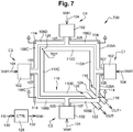
- FIG. 7 is a plan view illustrating a VCO 700 according to a further example embodiment of the present disclosure, and based on distributed active transformer series-coupled oscillator cores (SDAT).
- the VCO 700 has many features in common with the VCO 100 of Figure 1 , and like features have been referenced with like reference numerals and will not be described again in detail.
- the excitation circuits 102 of the oscillator cores C1 to C4 are positioned close to the mid-points of the sides of the square-shaped common inductive loop 110, and the inductive portions 106, 108 of a given oscillator core are formed adjacent to a same side of the square-shaped common inductive loop 110.
- the output lines 118, 122 are for example positioned at one corner of the common inductive loop 110
- the common-mode connection 126 is for example positioned at the opposite corner of the common inductive loop 110.
- oscillator cores in the embodiments of Figures 1 and 7 .
- a solution based on just two oscillator cores could be achieved by removing the cores C1 and C2, including their corresponding inductive portions 106A, 108D, 108A and 106B, or by removing the cores C3 and C4, including their corresponding inductive portions 106C, 108B, 108C and 106D.
- phase noise is proportional to the resonance tank resistance and inversely proportional to the square of the amplitude of the output signal.
- FIG 2 is a circuit diagram of the oscillator core C1 of Figures 1 and 7 according to an example embodiment.
- the other oscillator cores C2 to C4 are for example implemented by a similar circuit.
- the excitation circuit 102 for example comprises a varactor 202 controlled by the signal Vctrl, which is for example an analog control signal.
- the varactor 202 is coupled between the output lines 105, 107 of the excitation circuit 102.
- the circuit 102 also for example comprises a differential amplifier 206 (G m ) having its positive and negative differential outputs coupled to the output lines 105 and 107 respectively. Furthermore, the positive output of the amplifier 206 is coupled to its negative input, and the negative output of the amplifier 206 is coupled to its positive input.
- a resistor 204 shown by dashed lines in Figure 2 represents the tank resistance of the oscillator core, the resistances of the cores being presented in series in the embodiments of Figures 1 and 7 .
- the terminals of the varactor 202 may be short-circuited to VDD via switches 212, 214 respectively coupled between the lines 105, 107 and the VDD supply rail.
- the switches 212, 214 are implemented by relatively small MOS transistors, and are for example controlled by an enable signal EN, permitting the oscillator core to be selectively activated.
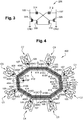
- FIG 3 is a circuit diagram of the differential amplifier 206 of the oscillator core of Figure 2 according to an example embodiment of the present disclosure.
- the differential amplifier 206 is implemented by a differential pair 304, 306, for example implemented by MOS or bipolar transistors, each coupled via its main current-conducting nodes between the output lines 105, 107 respectively and a ground voltage rail GND.
- the emitters or sources of the transistors 304, 306 may also be short-circuited to a common node in some embodiments, and the common node connected via a resistor or current source to the ground rail.
- the control nodes of the transistors 304, 306 are coupled together via resistors 308, 310.
- the control node of the transistor 304 is for example coupled to the output line 107 via a capacitor 312, and the control node of the transistor 306 is for example coupled to the output line 105 via a capacitor 314.
- Figure 3 provides merely one example implementation of the differential amplifier 206, there being many alternative circuits that could be used.
- the capacitors 312 and 314 could be replaced by short-circuits.
- Figures 1 and 7 are based on four oscillator cores, the shape of the common inductive loop can be adapted to more than four oscillator cores, as will now be described in more detail with reference to Figure 4 .
- FIG 4 schematically illustrates a VCO 400 according to a further example embodiment of the present disclosure, again based on distributed active transformer series-coupled oscillator cores (SDAT).
- the example of Figure 8 comprises eight oscillator cores C1 to C8 magnetically coupled in series, each oscillator core being implemented by a circuit similar to that of Figure 2 , including the excitation circuit 102.
- the oscillator cores C1 to C8 are coupled in series by electromagnetic induction, also known as inductive coupling, for example via a common inductive loop.
- Each oscillator core C1 to C8 of the VCO 400 has an inductive portion 406 coupled to the output line 105 of the excitation circuit 102, and an inductive portion 408 coupled to the output line 107 of the excitation circuit 102.
- the inductive portions 406, 408 are positioned adjacent to the sides of a common inductive loop 410.
- the common inductive loop 410 is octagon shaped, and each oscillator core C1 to C8 has its inductive portions 406, 408 formed adjacent to different sides of the inductive loop 410.
- the inductive portions 406, 408 of the oscillator cores are for example arranged to form segments of a primary slab of a one-to-one transformer, and the common inductive loop forms a secondary slab of the one-to-one transformer.
- an inductive portion 406A of the oscillator core C1 is formed adjacent to a side 410A of the common inductive loop 410
- an inductive portion 408H of the oscillator core C1 is formed adjacent to a side 410H of the common inductive loop 410
- the inductive portions 406B to 406H of the oscillator cores C2 to C8 are formed adjacent to sides 410B to 410H respectively of the common inductive loop 410
- the inductive portions 408A to 408G of the oscillator cores C2 to C8 are formed adjacent to the sides 410A to 410G respectively of the common inductive loop 410.
- Each of the inductive portions 406, 408 for example has an inductance in the range 10 to 100 pH, and for example 20 to 30 pH, for an oscillation frequency of around 50 GHz.
- Each pair of inductive portions 406A, 408A to 406H, 408H, formed adjacent to a same respective side 410A to 410H of the octagon-shaped common inductive loop 410 for example has one end coupled to a corresponding excitation circuit 102, and its other end coupled to a supply voltage rail at a point 414, thereby providing a virtual AC ground.
- the points 414 are coupled to the supply voltage rail VDD.
- each pair of inductive portions is formed by continuous strip of conductive track, the ends of each strip being coupled to the corresponding outputs of the corresponding excitation circuits 102 of a corresponding oscillator core, and the point 414 for example being the midpoint of each strip, which is for example coupled to the supply rail, such as VDD.
- Each continuous strip of conductive track forming a pair of the inductive portions 406, 408 for example has a length of between 50 and 150 ⁇ m, and for example of around 80 ⁇ m.
- the common inductive loop 410 for example comprises an octagon-shaped strip of conductive track that is continuous except along the side 410A, where it has one end 416 coupled to an output line 418 of the VCO 400, and its other end 420 coupled to an output line 422 of the VCO 400, the output lines 418, 422 respectively providing output signals OUT+, OUT- of the VCO 400.
- the ends 416, 420 of the inductive loop 110 are for example separated from each other by a spacing 424 at around the mid-point of the side 410A of the common inductive loop.
- a point 426 at around the midpoint of the opposite side 410E of the common inductive loop 410 is for example coupled to a common-mode supply voltage Vcm, which imposes a common-mode level on the differential output signals OUT+, OUT-.
- each of the oscillator cores C1 to C8 for example receives the same control voltage Vctrl, generated by a control circuit similar to the circuit 128 of Figure 1 .
- the excitation circuits 102 of the oscillator cores C1 to C8 of the VCO 400 could instead be positioned close to the mid-points of the sides of the octagon-shaped common inductive loop 410, and the inductive portions 406, 408 of a given oscillator core could be formed adjacent to a same side of the octagon-shaped common inductive loop 410.
- the output lines 418, 422 would for example be positioned at one of the vertices of the common inductive loop 410, and the common-mode connection 426 would for example be positioned at the opposite vertex, which is for example at exactly the middle of the common inductive loop 410.
- the embodiments of Figures 1 , 4 and 7 illustrate examples with four and eight oscillator cores respectively, more generally, there could be M cores, where M is equal to two or more. In some embodiments, M can be an odd integer.
- the gain in terms of phase noise reduction can be shown to be equal to 10 ⁇ Log 10 M dB when all cores are active.
- the common mode connection is for example coupled to the vertex opposite to the side on which the output lines of the VCO are formed and in particular at the middle of the inductive loop.
- Figure 8 illustrates an example of a VCO 800 based on five cores magnetically coupled in series via a pentagon-shaped inductive loop 110.
- the features of Figure 8 have been labelled with the same reference numerals as those of Figures 1 and 7 and will not be described again.
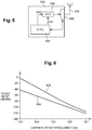
- FIG 5 schematically illustrates a wireless communications device 500 comprising a VCO 502 according to an example embodiment of the present disclosure.
- the VCO 502 is for example implemented by the circuit of Figure 1 , 4 , 7 or 8 or a similar circuit having M oscillator cores, wherein at least some of the cores can be selectively activated.
- the VCO 502 for example receives the control voltage Vctrl from a control circuit (CTRL) 504, and also an enable signal EN for each core capable of being selectively activated.
- An output signal from the VCO 502 is for example provided to an antenna circuit 506 coupled to an antenna 508. For example, this signal provides a carrier frequency for an RF transmission via the antenna 508.
- all of the oscillator cores of the VCO 502 are for example active, such that a signal having a relatively low phase noise is for example transmitted using the antenna 508.
- the control circuit 504 then for example evaluates the channel quality. For example, one or more frames or packets known to a receiver are transmitted to the receiver, which is thus able to evaluate the channel, and return the obtained channel estimation to the transmitter and in particular to the control circuit 504. If the quality is relatively high, the transmission for example continues based on the activation of all of the oscillator cores such that a relatively high transmission data rate can be obtained. If, however, the channel quality is found to be relatively poor, one or more of the oscillator cores is for example deactivated. Indeed, this can allow power consumption to be reduced in cases where reduced phase noise will not significantly improve channel bandwidth.
- Figure 6 is a graph representing single sideband phase noise (PHASE NOISE) spectral density in dBc/Hz, as a function of the offset from the carrier frequency in Hz, where dBc is the phase noise amplitude level referred to the carrier per 1 Hz bandwidth.
- a curve 602 illustrates an example based on a VCO having one core
- a curve 604 illustrates an example based on a VCO like the one of Figure 4 having 8 oscillator cores. In both cases, the VCOs were centered around the 60 GHz frequency range, and used BiCMOS transistor technology. It can be seen that 9 dB phase noise reduction is obtained at 1 MHz offset, where typically silicon based oscillators start to experience just the constant thermal noise effect (the curves of Figure 6 are nearly parallel).
- phase noise of a VCO is reduced while also providing a circuit arrangement that is feasible from a layout perspective. Furthermore, the addition of the oscillator core output signals leads to a differential output signal having relatively high amplitude, meaning in that in some cases amplification is not required. In some cases, an attenuator could be used to adjust the amplitude for a given application, while keeping the advantageously low phase noise.
- VCOs have been described in relation with Figures 1 , 4 , 7 and 8 based on regular polygon shaped transformers having 4, 5 and 8 sides, the principles described in relation with these figures could be extended to VCO with transformers having any regular polygon shape.
Landscapes
- Engineering & Computer Science (AREA)
- Power Engineering (AREA)
- Computer Networks & Wireless Communication (AREA)
- Signal Processing (AREA)
- Inductance-Capacitance Distribution Constants And Capacitance-Resistance Oscillators (AREA)
Abstract
Description
- This application claims the priority benefit of French patent application number
19/08586, filed on July 29, 2019 - The present disclosure relates generally to the field of voltage controlled oscillators (VCO), and in particular to a distributed active transformer VCO.
- Radio frequency wireless communications generally rely on VCOs for implementing the local oscillator at the transmitter and/or receiver, for example for generating carrier frequencies, clock generation, bit recovery, etc. The high growth in wireless communications, and the scarcity and license cost of reserving portions of the frequency spectrum, has increased the demand for the number of available frequency channels, particularly for mobile communications. This demand imposes increasingly stringent requirements on the amount of phase noise of the local oscillators. Indeed, phase noise strongly limits the frequency spectral efficiency of the communications over a wireless link.
- Furthermore, the importance of reducing phase noise in voltage controlled oscillators is not limited to the field of wireless communications, but is also pertinent in other fields such as integrated circuit clock generation, and also for sensing and radar applications.
- Phase noise generally corresponds to short term random frequency fluctuations of the sinusoidal waveform generated by the VCO.
- There is a need in the art for a VCO that can be implemented using silicon-based semiconductor technology, such as CMOS (Complementary MOS) or BiCMOS (Bipolar CMOS) technology, and which has relatively low phase noise.
- It is an aim of embodiments described herein to at least partially address one or needs in the prior art.
- According to one embodiment, there is provided a voltage controlled oscillator comprising a plurality of oscillator cores magnetically coupled in series. For example, the oscillator cores are coupled in series by electromagnetic induction, also known as inductive coupling, for example via a common inductive loop. For example, each oscillator core comprises first and second inductive portions, the first and second inductive portions of each of the oscillator cores being magnetically coupled to a common inductive loop, a first end of each of the first and second conductive portions being coupled to an excitation circuit of the oscillator core, and a second end of each of the first and second conductive portions being coupled to a voltage supply rail.
- According to one embodiment, the plurality of oscillator cores comprise M oscillator cores, with M equal to 4 or more.
- According to one embodiment, each oscillator core comprises first and second inductive portions, the first and second inductive portions of each of the oscillator cores being magnetically coupled to a common inductive loop.
- According to one embodiment, the voltage controlled oscillator further comprises a first output line coupled to one end of the common inductive loop and a second output line coupled to the other end of the common inductive loop.
- According to one embodiment, the common inductive loop forms a regular polygon shape having at least four sides, and the first and second inductive portions are positioned adjacent to the sides of the common inductive loop.
- According to one embodiment, the oscillator core has its first inductive portion positioned adjacent to a first side of the common inductive loop and its second inductive portion positioned adjacent to a second side of the common inductive loop, a first end of each of the first and second conductive portions being coupled to an excitation circuit of the oscillator core.
- According to one embodiment, the common inductive loop comprises: a common mode voltage connection at a mid-point along a first of its sides or at a vertex between two of the sides; and the first and second differential output lines coupled to a second of its sides opposite to the first side.
- According to one embodiment, each oscillator core comprises a varactor and a differential amplifier having a first output node coupled to one end of the first inductive portion and a second output node coupled to one end of the second inductive portion, the varactor being coupled between the first and second output nodes.
- According to one embodiment, each oscillator core is capable of being selectively activated.
- According to a further aspect, there is provided a communications device comprising: an antenna circuit for driving one or more antennas; and the above voltage controlled oscillator.
- The foregoing features and advantages, as well as others, will be described in detail in the following description of specific embodiments given by way of illustration and not limitation with reference to the accompanying drawings, in which:
- [
Fig. 1] Figure 1 is a plan view illustrating a VCO according to an example embodiment of the present disclosure; - [
Fig. 2] Figure 2 is a circuit diagram of an oscillator core ofFigure 1 according to an example embodiment; - [
Fig. 3] Figure 3 is a circuit diagram of a differential amplifier, corresponding to a Gm block of the oscillator core ofFigure 2 , according to an example embodiment of the present disclosure; - [
Fig. 4] Figure 4 schematically illustrates a VCO according to a further example embodiment of the present disclosure; - [
Fig. 5] Figure 5 schematically illustrates a wireless communications device comprising a VCO according to an example embodiment of the present disclosure; - [
Fig. 6] Figure 6 is a graph representing phase noise as a function of carrier offset frequency; - [
Fig. 7] Figure 7 schematically illustrates a VCO according to a further example embodiment of the present disclosure; and - [
Fig. 8] Figure 8 schematically illustrates a VCO according to yet a further example embodiment of the present disclosure. - Like features have been designated by like references in the various figures. In particular, the structural and/or functional features that are common among the various embodiments may have the same references and may dispose identical structural, dimensional and material properties.
- Unless indicated otherwise, when reference is made to two elements connected together, this signifies a direct connection without any intermediate elements other than conductors, and when reference is made to two elements linked or coupled together, this signifies that these two elements can be connected or they can be linked or coupled via one or more other elements.
- In the following disclosure, unless indicated otherwise, when reference is made to absolute positional qualifiers, such as the terms "front", "back", "top", "bottom", "left", "right", etc., or to relative positional qualifiers, such as the terms "above", "below", "higher", "lower", etc., or to qualifiers of orientation, such as "horizontal", "vertical", etc., reference is made to the orientation shown in the figures, or to a VCO as orientated during normal use.
- Unless specified otherwise, the expressions "around", "approximately", "substantially" and "in the order of" signify within 10 %, and preferably within 5 %.
- It has been proposed to reduce phase noise in a VCO by coupling several oscillator cores in parallel with each other. Indeed, the phase noise of a VCO has been shown to be proportional to its resistance, and by providing a plurality of oscillator cores arranged in parallel, this resistance can be reduced. The difficulty, however, is that the parallel coupling of several oscillator cores leads to particularly challenging or even insurmountable layout issues when the number of cores is equal to or greater than four.
-
Figure 1 is a plan view illustrating aVCO 100 according to an example embodiment of the present disclosure, and based on distributed active transformer series-coupled oscillator cores (SDAT). - The
VCO 100 in the example ofFigure 1 comprises four oscillator cores C1, C2, C3 and C4 that are magnetically coupled in series. For example, the oscillator cores are coupled in series by electromagnetic induction, also known as inductive coupling, for example via a common inductive loop. - Each oscillator core for example comprises an
excitation circuit 102 receiving a control signal Vctrl on aninput line 104, and havingoutputs output 105 of theexcitation circuit 102, and an inductive portion 108 coupled to theoutput 107 of theexcitation circuit 102. The inductive portions 106, 108 are positioned adjacent to the sides of a commoninductive loop 110. Thus, the inductive portions 106, 108 of the oscillator cores are for example arranged to form segments of a primary slab of a one-to-one transformer, and the common inductive loop forms a secondary slab of the one-to-one transformer. - In the example of
Figure 1 , the commoninductive loop 110 is square shaped, and each oscillator core has its inductive portions 106, 108 formed adjacent to different sides of theinductive loop 110. - For example, an
inductive portion 106A of the oscillator core C1 is formed adjacent to aside 110A of the commoninductive loop 110, and aninductive portion 108D of the oscillator core C1 is formed adjacent to aside 110D of the commoninductive loop 110. - Similarly: an
inductive portion 106B of the oscillator core C2 is formed adjacent to aside 110B of the commoninductive loop 110, and aninductive portion 108A of the oscillator core C2 is formed adjacent to theside 110A of the commoninductive loop 110; aninductive portion 106C of the oscillator core C3 is formed adjacent to aside 110C of the commoninductive loop 110, and aninductive portion 108B of the oscillator core C3 is formed adjacent to theside 110B of the commoninductive loop 110; and aninductive portion 106D of the oscillator core C4 is formed adjacent to aside 110D of the commoninductive loop 110, and aninductive portion 108C of the oscillator core C4 is formed adjacent to theside 110C of the commoninductive loop 110. - Each of the inductive portions 106, 108 for example has an inductance in the range 10 to 100 pH, and for example in the
range 20 to 30 pH, for an oscillation frequency of around 50 GHz. - Each pair of
inductive portions same side 110A to 110D of the square-shaped commoninductive loop 110 for example has one end coupled to acorresponding excitation circuit 102, and its other end coupled to a supply voltage rail at apoint 114, thereby providing a virtual AC ground. In the example ofFigure 1 , thepoints 114 are coupled to the supply voltage rail VDD. In some embodiments, each pair of inductive portions is formed by a continuous strip of conductive track, the ends of each strip being coupled to the corresponding outputs of theexcitation circuit 102 of a corresponding oscillator core, and thepoint 114 for example being the midpoint of each strip, which is for example coupled to the supply rail, such as VDD. Each continuous strip of conductive track forming a pair of the inductive portions 106, 108 for example has a total length of between 50 and 150 µm, and for example of around 80 µm. An advantage of coupling thepoints 114 to the supply voltage rail is that this provides a simple means for biasing each oscillator core, avoiding the use of DC decoupling capacitors. - The common
inductive loop 110 for example comprises a square-shaped strip of conductive track that is continuous except along theside 110A, where it has oneend 116 coupled to anoutput line 118 of theVCO 100, and itsother end 120 coupled to anoutput line 122 of theVCO 100, theoutput lines VCO 100. Theends inductive loop 110 are for example separated from each other by aspacing 124 at around the mid-point of theside 110A of the common inductive loop. Furthermore, apoint 126 at around the midpoint of theopposite side 110C of the commoninductive loop 110 is for example coupled to a common-mode supply voltage Vcm, which imposes a common-mode level on the differential output signals OUT+, OUT-. - Each of the oscillator cores C1 to C4 for example receives the same control voltage Vctrl, generated by a control circuit (CTRL) 128. For example, the
control circuit 128 forms part of a control loop and thus receives a feedback signal FB based on an evaluation of the frequency of the differential output signal OUT+, OUT-, and generates the control voltage Vctrl as a function of this feedback signal FB. - While, in the example of
Figure 1 , theexcitation circuits 102 of the oscillator cores C1 to C4 are positioned at corners of the square-shaped commoninductive loop 110, and the inductive portions 106, 108 are formed adjacent to different sides of the square-shaped commoninductive loop 110, other arrangements would be possible, as will now be described with reference toFigure 7 . -
Figure 7 is a plan view illustrating a VCO 700 according to a further example embodiment of the present disclosure, and based on distributed active transformer series-coupled oscillator cores (SDAT). The VCO 700 has many features in common with theVCO 100 ofFigure 1 , and like features have been referenced with like reference numerals and will not be described again in detail. In the VCO 700, theexcitation circuits 102 of the oscillator cores C1 to C4 are positioned close to the mid-points of the sides of the square-shaped commoninductive loop 110, and the inductive portions 106, 108 of a given oscillator core are formed adjacent to a same side of the square-shaped commoninductive loop 110. In this arrangement, theoutput lines inductive loop 110, and the common-mode connection 126 is for example positioned at the opposite corner of the commoninductive loop 110. - Furthermore, it would be possible to remove one or more oscillator cores in the embodiments of
Figures 1 and7 . For example, a solution based on just two oscillator cores could be achieved by removing the cores C1 and C2, including their correspondinginductive portions inductive portions - By providing oscillator cores magnetically coupled in series as shown in
Figures 1 and7 , the resistances of the cores will be added. However, the phase noise is still reduced. Indeed, it can be shown that phase noise is proportional to the resonance tank resistance and inversely proportional to the square of the amplitude of the output signal. By magnetically coupling a plurality of oscillator cores in series, their oscillations will sum up with each other, increasing the amplitude and allowing the phase noise to be reduced. -
Figure 2 is a circuit diagram of the oscillator core C1 ofFigures 1 and7 according to an example embodiment. The other oscillator cores C2 to C4 are for example implemented by a similar circuit. - The
excitation circuit 102 for example comprises avaractor 202 controlled by the signal Vctrl, which is for example an analog control signal. Thevaractor 202 is coupled between theoutput lines excitation circuit 102. Thecircuit 102 also for example comprises a differential amplifier 206 (Gm) having its positive and negative differential outputs coupled to theoutput lines amplifier 206 is coupled to its negative input, and the negative output of theamplifier 206 is coupled to its positive input. Aresistor 204 shown by dashed lines inFigure 2 represents the tank resistance of the oscillator core, the resistances of the cores being presented in series in the embodiments ofFigures 1 and7 . - While the
varactor 202 is shown connected between theoutput lines variant 210 shown inFigure 2 , the terminals of thevaractor 202, i.e. thelines switches 212, 214 respectively coupled between thelines switches 212, 214 are implemented by relatively small MOS transistors, and are for example controlled by an enable signal EN, permitting the oscillator core to be selectively activated. -
Figure 3 is a circuit diagram of thedifferential amplifier 206 of the oscillator core ofFigure 2 according to an example embodiment of the present disclosure. In the example ofFigure 3 , thedifferential amplifier 206 is implemented by adifferential pair output lines transistors transistors resistors transistor 304 is for example coupled to theoutput line 107 via acapacitor 312, and the control node of thetransistor 306 is for example coupled to theoutput line 105 via acapacitor 314. - Of course,
Figure 3 provides merely one example implementation of thedifferential amplifier 206, there being many alternative circuits that could be used. For example, in alternative embodiments, thecapacitors - While the examples of
Figures 1 and7 are based on four oscillator cores, the shape of the common inductive loop can be adapted to more than four oscillator cores, as will now be described in more detail with reference toFigure 4 . -
Figure 4 schematically illustrates aVCO 400 according to a further example embodiment of the present disclosure, again based on distributed active transformer series-coupled oscillator cores (SDAT). The example ofFigure 8 comprises eight oscillator cores C1 to C8 magnetically coupled in series, each oscillator core being implemented by a circuit similar to that ofFigure 2 , including theexcitation circuit 102. For example, the oscillator cores C1 to C8 are coupled in series by electromagnetic induction, also known as inductive coupling, for example via a common inductive loop. - Each oscillator core C1 to C8 of the
VCO 400 has an inductive portion 406 coupled to theoutput line 105 of theexcitation circuit 102, and an inductive portion 408 coupled to theoutput line 107 of theexcitation circuit 102. The inductive portions 406, 408 are positioned adjacent to the sides of a commoninductive loop 410. - In the example of
Figure 4 , the commoninductive loop 410 is octagon shaped, and each oscillator core C1 to C8 has its inductive portions 406, 408 formed adjacent to different sides of theinductive loop 410. Thus, the inductive portions 406, 408 of the oscillator cores are for example arranged to form segments of a primary slab of a one-to-one transformer, and the common inductive loop forms a secondary slab of the one-to-one transformer. - For example, an
inductive portion 406A of the oscillator core C1 is formed adjacent to aside 410A of the commoninductive loop 410, and an inductive portion 408H of the oscillator core C1 is formed adjacent to aside 410H of the commoninductive loop 410. Similarly, theinductive portions 406B to 406H of the oscillator cores C2 to C8 are formed adjacent to sides 410B to 410H respectively of the commoninductive loop 410, and theinductive portions 408A to 408G of the oscillator cores C2 to C8 are formed adjacent to thesides 410A to 410G respectively of the commoninductive loop 410. - Each of the inductive portions 406, 408 for example has an inductance in the range 10 to 100 pH, and for example 20 to 30 pH, for an oscillation frequency of around 50 GHz.
- Each pair of
inductive portions respective side 410A to 410H of the octagon-shaped commoninductive loop 410 for example has one end coupled to acorresponding excitation circuit 102, and its other end coupled to a supply voltage rail at apoint 414, thereby providing a virtual AC ground. In the example ofFigure 4 , thepoints 414 are coupled to the supply voltage rail VDD. In some embodiments, each pair of inductive portions is formed by continuous strip of conductive track, the ends of each strip being coupled to the corresponding outputs of the correspondingexcitation circuits 102 of a corresponding oscillator core, and thepoint 414 for example being the midpoint of each strip, which is for example coupled to the supply rail, such as VDD. Each continuous strip of conductive track forming a pair of the inductive portions 406, 408 for example has a length of between 50 and 150 µm, and for example of around 80 µm. An advantage of coupling thepoints 414 to the supply voltage rail is that this provides a simple means for biasing each oscillator core, avoiding the use of DC decoupling capacitors. - The common
inductive loop 410 for example comprises an octagon-shaped strip of conductive track that is continuous except along theside 410A, where it has one end 416 coupled to anoutput line 418 of theVCO 400, and itsother end 420 coupled to anoutput line 422 of theVCO 400, theoutput lines VCO 400. The ends 416, 420 of theinductive loop 110 are for example separated from each other by a spacing 424 at around the mid-point of theside 410A of the common inductive loop. Furthermore, apoint 426 at around the midpoint of theopposite side 410E of the commoninductive loop 410 is for example coupled to a common-mode supply voltage Vcm, which imposes a common-mode level on the differential output signals OUT+, OUT-. - While not shown in
Figure 4 , each of the oscillator cores C1 to C8 for example receives the same control voltage Vctrl, generated by a control circuit similar to thecircuit 128 ofFigure 1 . - Like for the embodiment of
Figure 7 , theexcitation circuits 102 of the oscillator cores C1 to C8 of theVCO 400 could instead be positioned close to the mid-points of the sides of the octagon-shaped commoninductive loop 410, and the inductive portions 406, 408 of a given oscillator core could be formed adjacent to a same side of the octagon-shaped commoninductive loop 410. In such an arrangement, theoutput lines inductive loop 410, and the common-mode connection 426 would for example be positioned at the opposite vertex, which is for example at exactly the middle of the commoninductive loop 410. - Furthermore, it would be possible to remove one or more oscillator cores from the
VCO 400. For example, a solution based on six oscillator cores could be achieved by removing the cores C1 and C2. - While the embodiments of
Figures 1 ,4 and7 illustrate examples with four and eight oscillator cores respectively, more generally, there could be M cores, where M is equal to two or more. In some embodiments, M can be an odd integer. The gain in terms of phase noise reduction can be shown to be equal to 10∗Log10M dB when all cores are active. Thus the gain in the example ofFigures 1 ,4 and7 with M=4 is for example 6 dB of phase noise reduction, and the gain in the example ofFigure 4 with M=8 is for example 9 dB of phase noise reduction. In the case of an odd number of cores, the common mode connection is for example coupled to the vertex opposite to the side on which the output lines of the VCO are formed and in particular at the middle of the inductive loop. -
Figure 8 illustrates an example of aVCO 800 based on five cores magnetically coupled in series via a pentagon-shapedinductive loop 110. The features ofFigure 8 have been labelled with the same reference numerals as those ofFigures 1 and7 and will not be described again. However, inFigure 8 , there areadditional references - Furthermore, it would also be possible, in the embodiments of
Figure 1 and4 , or more generally in embodiments with M oscillator cores magnetically coupled in series, to selectively activate only certain cores. For example some or all of the oscillator cores include thevariant 210 ofFigure 2 , as will now be described in more detail with reference toFigure 5 . -
Figure 5 schematically illustrates awireless communications device 500 comprising aVCO 502 according to an example embodiment of the present disclosure. TheVCO 502 is for example implemented by the circuit ofFigure 1 ,4 ,7 or8 or a similar circuit having M oscillator cores, wherein at least some of the cores can be selectively activated. TheVCO 502 for example receives the control voltage Vctrl from a control circuit (CTRL) 504, and also an enable signal EN for each core capable of being selectively activated. An output signal from theVCO 502 is for example provided to anantenna circuit 506 coupled to anantenna 508. For example, this signal provides a carrier frequency for an RF transmission via theantenna 508. - In operation, initially all of the oscillator cores of the
VCO 502 are for example active, such that a signal having a relatively low phase noise is for example transmitted using theantenna 508. Thecontrol circuit 504 then for example evaluates the channel quality. For example, one or more frames or packets known to a receiver are transmitted to the receiver, which is thus able to evaluate the channel, and return the obtained channel estimation to the transmitter and in particular to thecontrol circuit 504. If the quality is relatively high, the transmission for example continues based on the activation of all of the oscillator cores such that a relatively high transmission data rate can be obtained. If, however, the channel quality is found to be relatively poor, one or more of the oscillator cores is for example deactivated. Indeed, this can allow power consumption to be reduced in cases where reduced phase noise will not significantly improve channel bandwidth. -
Figure 6 is a graph representing single sideband phase noise (PHASE NOISE) spectral density in dBc/Hz, as a function of the offset from the carrier frequency in Hz, where dBc is the phase noise amplitude level referred to the carrier per 1 Hz bandwidth. Acurve 602 illustrates an example based on a VCO having one core, and acurve 604 illustrates an example based on a VCO like the one ofFigure 4 having 8 oscillator cores. In both cases, the VCOs were centered around the 60 GHz frequency range, and used BiCMOS transistor technology. It can be seen that 9 dB phase noise reduction is obtained at 1 MHz offset, where typically silicon based oscillators start to experience just the constant thermal noise effect (the curves ofFigure 6 are nearly parallel). - Advantages of the embodiments described herein is that the phase noise of a VCO is reduced while also providing a circuit arrangement that is feasible from a layout perspective. Furthermore, the addition of the oscillator core output signals leads to a differential output signal having relatively high amplitude, meaning in that in some cases amplification is not required. In some cases, an attenuator could be used to adjust the amplitude for a given application, while keeping the advantageously low phase noise.
- Various embodiments and variants have been described. Those skilled in the art will understand that certain features of these embodiments can be combined and other variants will readily occur to those skilled in the art. In particular, while embodiments have been described in which a differential amplifier of the excitation circuit is connected or coupled to a ground rail, and inductive portions of the oscillator cores are connected or coupled to a positive supply rail, in alternative embodiments the supply voltages of the oscillator cores could be inverted.
- Furthermore, while embodiments of VCOs have been described in relation with
Figures 1 ,4 ,7 and8 based on regular polygon shaped transformers having 4, 5 and 8 sides, the principles described in relation with these figures could be extended to VCO with transformers having any regular polygon shape. - Furthermore, while examples based on BiCMOS transistor technology have been described, it will be apparent to those skilled in the art that in alternative embodiments other transistor technologies, such as pure bipolar, or CMOS, could be used.
Claims (10)
- A voltage controlled oscillator comprising a plurality of oscillator cores (C1 to C8) magnetically coupled in series.
- The voltage controlled oscillator of claim 1, wherein the plurality of oscillator cores comprise M oscillator cores (C1 to C8), with M equal to 4 or more.
- The voltage controlled oscillator of claim 1 or 2, wherein each oscillator core (C1 to C8) comprises first and second inductive portions (106, 108, 406, 408), the first and second inductive portions of each of the oscillator cores being magnetically coupled to a common inductive loop (110, 410) .
- The voltage controlled oscillator of claim 3, further comprising a first output line (118, 418) coupled to one end (116, 416) of the common inductive loop (110, 410) and a second output line (122, 422) coupled to the other end (120) of the common inductive loop.
- The voltage controlled oscillator of claim 3 or 4, wherein the common inductive loop (110, 410) forms a regular polygon shape having at least four sides, and the first and second inductive portions (106, 108, 406, 408) are positioned adjacent to the sides of the common inductive loop.
- The voltage controlled oscillator of claim 5, wherein each oscillator core (C1 to C8) has its first inductive portion (106, 406) positioned adjacent to a first side of the common inductive loop (110, 410) and its second inductive portion (108, 408) positioned adjacent to a second side of the common inductive loop, a first end of each of the first and second conductive portions being coupled to an excitation circuit (102) of the oscillator core.
- The voltage controlled oscillator of claim 5 or 6, wherein the common inductive loop (110, 410) comprises:- a common mode voltage connection at a mid-point (126, 426) along a first of its sides (110C, 410E) or at a vertex between two of the sides; and- the first and second differential output lines (418, 422) coupled to a second of its sides opposite to the first side.
- The voltage controlled oscillator of any of claims 3 to 7, wherein each oscillator core (C1 to C8) comprises a varactor (202) and a differential amplifier having a first output node (105, 405) coupled to one end of the first inductive portion (106, 406) and a second output node (107, 407) coupled to one end of the second inductive portion (108, 408), the varactor (202) being coupled between the first and second output nodes.
- The voltage controlled oscillator of any of claims 1 to 8, wherein each oscillator core (C1 to C8) is capable of being selectively activated.
- A communications device comprising:- an antenna circuit (506) for driving one or more antennas (508); and- the voltage controlled oscillator of any preceding claim.
Applications Claiming Priority (1)
| Application Number | Priority Date | Filing Date | Title |
|---|---|---|---|
| FR1908586A FR3099667A1 (en) | 2019-07-29 | 2019-07-29 | Distributed active transformer voltage controlled oscillator |
Publications (2)
| Publication Number | Publication Date |
|---|---|
| EP3772176A1 true EP3772176A1 (en) | 2021-02-03 |
| EP3772176B1 EP3772176B1 (en) | 2024-03-06 |
Family
ID=68733296
Family Applications (1)
| Application Number | Title | Priority Date | Filing Date |
|---|---|---|---|
| EP20186349.5A Active EP3772176B1 (en) | 2019-07-29 | 2020-07-17 | Voltage controlled oscillator based on a distributed active transformer |
Country Status (4)
| Country | Link |
|---|---|
| US (1) | US11171600B2 (en) |
| EP (1) | EP3772176B1 (en) |
| CN (2) | CN212677126U (en) |
| FR (1) | FR3099667A1 (en) |
Families Citing this family (4)
| Publication number | Priority date | Publication date | Assignee | Title |
|---|---|---|---|---|
| FR3099667A1 (en) * | 2019-07-29 | 2021-02-05 | Stmicroelectronics S.R.L. | Distributed active transformer voltage controlled oscillator |
| US11837995B2 (en) * | 2021-05-25 | 2023-12-05 | Mediatek Inc. | One-coil multi-core inductor-capacitor oscillator |
| US12609653B2 (en) | 2024-07-22 | 2026-04-21 | Samsung Electronics Co., Ltd. | Multi-core VCO with robust unwanted mode suppression and circular coil topology |
| CN121036694B (en) * | 2025-07-17 | 2026-05-05 | 华南理工大学 | A tapped inductor, resonant cavity structure, oscillator structure, chip, and device. |
Citations (3)
| Publication number | Priority date | Publication date | Assignee | Title |
|---|---|---|---|---|
| US20040124931A1 (en) * | 2002-10-18 | 2004-07-01 | Seyed-Ali Hajimiri | Circular geometry oscillators |
| US20140070898A1 (en) * | 2012-09-11 | 2014-03-13 | Broadcom Corporation | Low Phase Noise Voltage Controlled Oscillators |
| EP3416284A1 (en) * | 2017-06-15 | 2018-12-19 | Commissariat à l'Energie Atomique et aux Energies Alternatives | Architecture for sharing voltage between two oscillators |
Family Cites Families (25)
| Publication number | Priority date | Publication date | Assignee | Title |
|---|---|---|---|---|
| EP1400012B1 (en) * | 2000-10-10 | 2011-08-31 | California Institute Of Technology | Distributed circular geometry power amplifier architecture |
| US6856199B2 (en) * | 2000-10-10 | 2005-02-15 | California Institute Of Technology | Reconfigurable distributed active transformers |
| SE0102420D0 (en) * | 2001-07-05 | 2001-07-05 | Ericsson Telefon Ab L M | Oscillator |
| TWI326967B (en) * | 2002-03-11 | 2010-07-01 | California Inst Of Techn | Differential amplifier |
| TW200520121A (en) * | 2003-08-28 | 2005-06-16 | Gct Semiconductor Inc | Integrated circuit package having an inductance loop formed from a multi-loop configuration |
| US7095283B2 (en) * | 2003-10-28 | 2006-08-22 | Axiom Microdevices, Inc. | Supply circuit for power amplifier drivers |
| WO2006127851A2 (en) * | 2005-05-24 | 2006-11-30 | The Trustees Of Columbia University In The City Of New York | Systems and methods for reducing circuit area |
| DE102007022999A1 (en) * | 2007-05-15 | 2008-11-27 | Atmel Duisburg Gmbh | oscillator |
| IT1392575B1 (en) * | 2008-12-30 | 2012-03-09 | St Microelectronics Rousset | AMPLIFIER WITH DIFFERENTIAL POWER COMBINATOR, WITH DISTRIBUTED ACTIVE TRANSFORMER |
| FR2947118B1 (en) * | 2009-06-19 | 2011-06-10 | St Ericsson Sa St Ericsson Ltd | FREQUENCY MULTIBAND OSCILLATOR DEVICE |
| US8183948B2 (en) * | 2009-09-13 | 2012-05-22 | International Business Machines Corporation | Ultra-compact PLL with wide tuning range and low noise |
| US8558625B1 (en) * | 2009-11-13 | 2013-10-15 | The United States Of America As Represented By The Secretary Of The Navy | Frequency tuning and phase shifting techniques using 1-dimensional coupled voltage-controlled-oscillator arrays for active antennas |
| US8797105B2 (en) * | 2011-10-04 | 2014-08-05 | Cornell University | Tunable signal source |
| US9130505B2 (en) * | 2011-11-10 | 2015-09-08 | Qualcomm Incorporated | Multi-frequency reconfigurable voltage controlled oscillator (VCO) and method of providing same |
| US9559702B1 (en) * | 2013-09-30 | 2017-01-31 | Marvell International Ltd. | Circuits and methods for flicker noise upconversion minimization in an oscillator |
| US9191014B2 (en) * | 2013-11-08 | 2015-11-17 | Taiwan Semiconductor Manufacturing Company, Ltd. | Method and apparatus of synchronizing oscillators |
| US9722537B2 (en) * | 2014-08-20 | 2017-08-01 | Short Circuit Technologies Llc | Fractional-N frequency synthesizer incorporating cyclic digital-to-time and time-to-digital circuit pair |
| US9425737B1 (en) * | 2015-03-16 | 2016-08-23 | Futurewei Technologies, Inc. | Tapped inductor voltage controlled oscillator |
| WO2016209287A1 (en) * | 2015-06-26 | 2016-12-29 | Olympus Corporation | Tuned offset phase-locked loop transmitter |
| US9543892B1 (en) * | 2015-07-16 | 2017-01-10 | Qualcomm Incorporated | Overlapping uncoupled inductors for low-cost multi-frequency voltage-controlled oscillators |
| US9356556B1 (en) * | 2015-08-06 | 2016-05-31 | Xilinx, Inc. | Circuits for and methods of implementing a dual-mode oscillator |
| US9831830B2 (en) * | 2015-08-21 | 2017-11-28 | International Business Machines Corporation | Bipolar junction transistor based switched capacitors |
| US9559667B1 (en) * | 2015-08-21 | 2017-01-31 | International Business Machines Corporation | Oscillator phase noise using active device stacking |
| ITUB20154230A1 (en) | 2015-10-08 | 2017-04-08 | St Microelectronics Srl | CIRCUIT OSCILLATOR, EQUIPMENT AND CORRESPONDENT PROCEDURE " |
| FR3099667A1 (en) * | 2019-07-29 | 2021-02-05 | Stmicroelectronics S.R.L. | Distributed active transformer voltage controlled oscillator |
-
2019
- 2019-07-29 FR FR1908586A patent/FR3099667A1/en not_active Ceased
-
2020
- 2020-07-17 EP EP20186349.5A patent/EP3772176B1/en active Active
- 2020-07-23 US US16/937,071 patent/US11171600B2/en active Active
- 2020-07-29 CN CN202021534398.4U patent/CN212677126U/en active Active
- 2020-07-29 CN CN202010746248.8A patent/CN112311330B/en active Active
Patent Citations (3)
| Publication number | Priority date | Publication date | Assignee | Title |
|---|---|---|---|---|
| US20040124931A1 (en) * | 2002-10-18 | 2004-07-01 | Seyed-Ali Hajimiri | Circular geometry oscillators |
| US20140070898A1 (en) * | 2012-09-11 | 2014-03-13 | Broadcom Corporation | Low Phase Noise Voltage Controlled Oscillators |
| EP3416284A1 (en) * | 2017-06-15 | 2018-12-19 | Commissariat à l'Energie Atomique et aux Energies Alternatives | Architecture for sharing voltage between two oscillators |
Also Published As
| Publication number | Publication date |
|---|---|
| FR3099667A1 (en) | 2021-02-05 |
| CN112311330B (en) | 2025-11-07 |
| US20210036659A1 (en) | 2021-02-04 |
| CN112311330A (en) | 2021-02-02 |
| CN212677126U (en) | 2021-03-09 |
| US11171600B2 (en) | 2021-11-09 |
| EP3772176B1 (en) | 2024-03-06 |
Similar Documents
| Publication | Publication Date | Title |
|---|---|---|
| EP3772176B1 (en) | Voltage controlled oscillator based on a distributed active transformer | |
| Bhat et al. | 26.3 A 25-to-38GHz, 195dB FoMT LC QVCO in 65nm LP CMOS using a 4-port dual-mode resonator for 5G radios | |
| EP2575259B1 (en) | Voltage-controlled oscillators and related systems | |
| US20100301955A1 (en) | Frequency divider using an injection-locking-range enhancement technique | |
| WO2012166502A1 (en) | Method and apparatus for local oscillation distribution | |
| US8742880B2 (en) | Single differential transformer core | |
| US20100171557A1 (en) | Voltage controlled oscillator, and pll circuit and wirless communication device each using the same | |
| KR100691281B1 (en) | Quadrature Voltage Controlled Oscillators | |
| US20050046500A1 (en) | Tunable frequency, low phase noise and low thermal drift oscillator | |
| KR20050053779A (en) | Circular geometry oscillators | |
| CN101212198B (en) | Voltage controlled oscillator | |
| US8717112B2 (en) | Inductance-capacitance (LC) oscillator | |
| CN207603629U (en) | Local oscillator equipment and transceiver system | |
| US11936339B2 (en) | Voltage controlled oscillator with series resonant circuit | |
| US20060033586A1 (en) | Low noise, hybrid tuned wideband voltage controlled oscillator | |
| US9099957B2 (en) | Voltage-controlled oscillators and related systems | |
| US6842081B2 (en) | Dual frequency voltage controlled oscillator circuit | |
| US7538630B2 (en) | Voltage controlled oscillator | |
| US6690244B2 (en) | Low phase-noise integrated voltage controlled oscillator | |
| US12057810B2 (en) | Voltage controlled oscillator for flipped and complementary low noise | |
| CN114073006B (en) | Ring oscillator with resonant circuit | |
| US7598817B2 (en) | Oscillator for outputting different oscillation frequencies | |
| KR19980063973A (en) | Oscillation Circuit | |
| EP2636145B1 (en) | An oscillator circuit with feedback | |
| EP1926207A1 (en) | Low noise, hybrid tuned wideband voltage controlled oscillator |
Legal Events
| Date | Code | Title | Description |
|---|---|---|---|
| PUAI | Public reference made under article 153(3) epc to a published international application that has entered the european phase |
Free format text: ORIGINAL CODE: 0009012 |
|
| STAA | Information on the status of an ep patent application or granted ep patent |
Free format text: STATUS: REQUEST FOR EXAMINATION WAS MADE |
|
| 17P | Request for examination filed |
Effective date: 20200717 |
|
| AK | Designated contracting states |
Kind code of ref document: A1 Designated state(s): AL AT BE BG CH CY CZ DE DK EE ES FI FR GB GR HR HU IE IS IT LI LT LU LV MC MK MT NL NO PL PT RO RS SE SI SK SM TR |
|
| AX | Request for extension of the european patent |
Extension state: BA ME |
|
| STAA | Information on the status of an ep patent application or granted ep patent |
Free format text: STATUS: EXAMINATION IS IN PROGRESS |
|
| 17Q | First examination report despatched |
Effective date: 20220317 |
|
| GRAP | Despatch of communication of intention to grant a patent |
Free format text: ORIGINAL CODE: EPIDOSNIGR1 |
|
| STAA | Information on the status of an ep patent application or granted ep patent |
Free format text: STATUS: GRANT OF PATENT IS INTENDED |
|
| RIC1 | Information provided on ipc code assigned before grant |
Ipc: H03B 5/12 20060101AFI20231018BHEP |
|
| INTG | Intention to grant announced |
Effective date: 20231117 |
|
| GRAS | Grant fee paid |
Free format text: ORIGINAL CODE: EPIDOSNIGR3 |
|
| GRAA | (expected) grant |
Free format text: ORIGINAL CODE: 0009210 |
|
| STAA | Information on the status of an ep patent application or granted ep patent |
Free format text: STATUS: THE PATENT HAS BEEN GRANTED |
|
| AK | Designated contracting states |
Kind code of ref document: B1 Designated state(s): AL AT BE BG CH CY CZ DE DK EE ES FI FR GB GR HR HU IE IS IT LI LT LU LV MC MK MT NL NO PL PT RO RS SE SI SK SM TR |
|
| REG | Reference to a national code |
Ref country code: CH Ref legal event code: EP |
|
| REG | Reference to a national code |
Ref country code: IE Ref legal event code: FG4D |
|
| REG | Reference to a national code |
Ref country code: DE Ref legal event code: R096 Ref document number: 602020026689 Country of ref document: DE |
|
| REG | Reference to a national code |
Ref country code: LT Ref legal event code: MG9D |
|
| PG25 | Lapsed in a contracting state [announced via postgrant information from national office to epo] |
Ref country code: LT Free format text: LAPSE BECAUSE OF FAILURE TO SUBMIT A TRANSLATION OF THE DESCRIPTION OR TO PAY THE FEE WITHIN THE PRESCRIBED TIME-LIMIT Effective date: 20240306 |
|
| REG | Reference to a national code |
Ref country code: NL Ref legal event code: MP Effective date: 20240306 |
|
| PG25 | Lapsed in a contracting state [announced via postgrant information from national office to epo] |
Ref country code: GR Free format text: LAPSE BECAUSE OF FAILURE TO SUBMIT A TRANSLATION OF THE DESCRIPTION OR TO PAY THE FEE WITHIN THE PRESCRIBED TIME-LIMIT Effective date: 20240607 |
|
| PG25 | Lapsed in a contracting state [announced via postgrant information from national office to epo] |
Ref country code: HR Free format text: LAPSE BECAUSE OF FAILURE TO SUBMIT A TRANSLATION OF THE DESCRIPTION OR TO PAY THE FEE WITHIN THE PRESCRIBED TIME-LIMIT Effective date: 20240306 Ref country code: RS Free format text: LAPSE BECAUSE OF FAILURE TO SUBMIT A TRANSLATION OF THE DESCRIPTION OR TO PAY THE FEE WITHIN THE PRESCRIBED TIME-LIMIT Effective date: 20240606 |
|
| PG25 | Lapsed in a contracting state [announced via postgrant information from national office to epo] |
Ref country code: ES Free format text: LAPSE BECAUSE OF FAILURE TO SUBMIT A TRANSLATION OF THE DESCRIPTION OR TO PAY THE FEE WITHIN THE PRESCRIBED TIME-LIMIT Effective date: 20240306 |
|
| PG25 | Lapsed in a contracting state [announced via postgrant information from national office to epo] |
Ref country code: RS Free format text: LAPSE BECAUSE OF FAILURE TO SUBMIT A TRANSLATION OF THE DESCRIPTION OR TO PAY THE FEE WITHIN THE PRESCRIBED TIME-LIMIT Effective date: 20240606 Ref country code: NO Free format text: LAPSE BECAUSE OF FAILURE TO SUBMIT A TRANSLATION OF THE DESCRIPTION OR TO PAY THE FEE WITHIN THE PRESCRIBED TIME-LIMIT Effective date: 20240606 Ref country code: LT Free format text: LAPSE BECAUSE OF FAILURE TO SUBMIT A TRANSLATION OF THE DESCRIPTION OR TO PAY THE FEE WITHIN THE PRESCRIBED TIME-LIMIT Effective date: 20240306 Ref country code: HR Free format text: LAPSE BECAUSE OF FAILURE TO SUBMIT A TRANSLATION OF THE DESCRIPTION OR TO PAY THE FEE WITHIN THE PRESCRIBED TIME-LIMIT Effective date: 20240306 Ref country code: GR Free format text: LAPSE BECAUSE OF FAILURE TO SUBMIT A TRANSLATION OF THE DESCRIPTION OR TO PAY THE FEE WITHIN THE PRESCRIBED TIME-LIMIT Effective date: 20240607 Ref country code: FI Free format text: LAPSE BECAUSE OF FAILURE TO SUBMIT A TRANSLATION OF THE DESCRIPTION OR TO PAY THE FEE WITHIN THE PRESCRIBED TIME-LIMIT Effective date: 20240306 Ref country code: ES Free format text: LAPSE BECAUSE OF FAILURE TO SUBMIT A TRANSLATION OF THE DESCRIPTION OR TO PAY THE FEE WITHIN THE PRESCRIBED TIME-LIMIT Effective date: 20240306 Ref country code: BG Free format text: LAPSE BECAUSE OF FAILURE TO SUBMIT A TRANSLATION OF THE DESCRIPTION OR TO PAY THE FEE WITHIN THE PRESCRIBED TIME-LIMIT Effective date: 20240306 |
|
| REG | Reference to a national code |
Ref country code: AT Ref legal event code: MK05 Ref document number: 1664524 Country of ref document: AT Kind code of ref document: T Effective date: 20240306 |
|
| PG25 | Lapsed in a contracting state [announced via postgrant information from national office to epo] |
Ref country code: SE Free format text: LAPSE BECAUSE OF FAILURE TO SUBMIT A TRANSLATION OF THE DESCRIPTION OR TO PAY THE FEE WITHIN THE PRESCRIBED TIME-LIMIT Effective date: 20240306 Ref country code: LV Free format text: LAPSE BECAUSE OF FAILURE TO SUBMIT A TRANSLATION OF THE DESCRIPTION OR TO PAY THE FEE WITHIN THE PRESCRIBED TIME-LIMIT Effective date: 20240306 |
|
| PG25 | Lapsed in a contracting state [announced via postgrant information from national office to epo] |
Ref country code: NL Free format text: LAPSE BECAUSE OF FAILURE TO SUBMIT A TRANSLATION OF THE DESCRIPTION OR TO PAY THE FEE WITHIN THE PRESCRIBED TIME-LIMIT Effective date: 20240306 |
|
| PG25 | Lapsed in a contracting state [announced via postgrant information from national office to epo] |
Ref country code: NL Free format text: LAPSE BECAUSE OF FAILURE TO SUBMIT A TRANSLATION OF THE DESCRIPTION OR TO PAY THE FEE WITHIN THE PRESCRIBED TIME-LIMIT Effective date: 20240306 |
|
| PG25 | Lapsed in a contracting state [announced via postgrant information from national office to epo] |
Ref country code: IS Free format text: LAPSE BECAUSE OF FAILURE TO SUBMIT A TRANSLATION OF THE DESCRIPTION OR TO PAY THE FEE WITHIN THE PRESCRIBED TIME-LIMIT Effective date: 20240706 |
|
| PG25 | Lapsed in a contracting state [announced via postgrant information from national office to epo] |
Ref country code: PT Free format text: LAPSE BECAUSE OF FAILURE TO SUBMIT A TRANSLATION OF THE DESCRIPTION OR TO PAY THE FEE WITHIN THE PRESCRIBED TIME-LIMIT Effective date: 20240708 Ref country code: SM Free format text: LAPSE BECAUSE OF FAILURE TO SUBMIT A TRANSLATION OF THE DESCRIPTION OR TO PAY THE FEE WITHIN THE PRESCRIBED TIME-LIMIT Effective date: 20240306 |
|
| PG25 | Lapsed in a contracting state [announced via postgrant information from national office to epo] |
Ref country code: EE Free format text: LAPSE BECAUSE OF FAILURE TO SUBMIT A TRANSLATION OF THE DESCRIPTION OR TO PAY THE FEE WITHIN THE PRESCRIBED TIME-LIMIT Effective date: 20240306 Ref country code: CZ Free format text: LAPSE BECAUSE OF FAILURE TO SUBMIT A TRANSLATION OF THE DESCRIPTION OR TO PAY THE FEE WITHIN THE PRESCRIBED TIME-LIMIT Effective date: 20240306 |
|
| PG25 | Lapsed in a contracting state [announced via postgrant information from national office to epo] |
Ref country code: AT Free format text: LAPSE BECAUSE OF FAILURE TO SUBMIT A TRANSLATION OF THE DESCRIPTION OR TO PAY THE FEE WITHIN THE PRESCRIBED TIME-LIMIT Effective date: 20240306 |
|
| PG25 | Lapsed in a contracting state [announced via postgrant information from national office to epo] |
Ref country code: PL Free format text: LAPSE BECAUSE OF FAILURE TO SUBMIT A TRANSLATION OF THE DESCRIPTION OR TO PAY THE FEE WITHIN THE PRESCRIBED TIME-LIMIT Effective date: 20240306 |
|
| PG25 | Lapsed in a contracting state [announced via postgrant information from national office to epo] |
Ref country code: SK Free format text: LAPSE BECAUSE OF FAILURE TO SUBMIT A TRANSLATION OF THE DESCRIPTION OR TO PAY THE FEE WITHIN THE PRESCRIBED TIME-LIMIT Effective date: 20240306 |
|
| PG25 | Lapsed in a contracting state [announced via postgrant information from national office to epo] |
Ref country code: SM Free format text: LAPSE BECAUSE OF FAILURE TO SUBMIT A TRANSLATION OF THE DESCRIPTION OR TO PAY THE FEE WITHIN THE PRESCRIBED TIME-LIMIT Effective date: 20240306 Ref country code: SK Free format text: LAPSE BECAUSE OF FAILURE TO SUBMIT A TRANSLATION OF THE DESCRIPTION OR TO PAY THE FEE WITHIN THE PRESCRIBED TIME-LIMIT Effective date: 20240306 Ref country code: RO Free format text: LAPSE BECAUSE OF FAILURE TO SUBMIT A TRANSLATION OF THE DESCRIPTION OR TO PAY THE FEE WITHIN THE PRESCRIBED TIME-LIMIT Effective date: 20240306 Ref country code: PT Free format text: LAPSE BECAUSE OF FAILURE TO SUBMIT A TRANSLATION OF THE DESCRIPTION OR TO PAY THE FEE WITHIN THE PRESCRIBED TIME-LIMIT Effective date: 20240708 Ref country code: PL Free format text: LAPSE BECAUSE OF FAILURE TO SUBMIT A TRANSLATION OF THE DESCRIPTION OR TO PAY THE FEE WITHIN THE PRESCRIBED TIME-LIMIT Effective date: 20240306 Ref country code: IS Free format text: LAPSE BECAUSE OF FAILURE TO SUBMIT A TRANSLATION OF THE DESCRIPTION OR TO PAY THE FEE WITHIN THE PRESCRIBED TIME-LIMIT Effective date: 20240706 Ref country code: EE Free format text: LAPSE BECAUSE OF FAILURE TO SUBMIT A TRANSLATION OF THE DESCRIPTION OR TO PAY THE FEE WITHIN THE PRESCRIBED TIME-LIMIT Effective date: 20240306 Ref country code: CZ Free format text: LAPSE BECAUSE OF FAILURE TO SUBMIT A TRANSLATION OF THE DESCRIPTION OR TO PAY THE FEE WITHIN THE PRESCRIBED TIME-LIMIT Effective date: 20240306 Ref country code: AT Free format text: LAPSE BECAUSE OF FAILURE TO SUBMIT A TRANSLATION OF THE DESCRIPTION OR TO PAY THE FEE WITHIN THE PRESCRIBED TIME-LIMIT Effective date: 20240306 |
|
| PG25 | Lapsed in a contracting state [announced via postgrant information from national office to epo] |
Ref country code: IT Free format text: LAPSE BECAUSE OF FAILURE TO SUBMIT A TRANSLATION OF THE DESCRIPTION OR TO PAY THE FEE WITHIN THE PRESCRIBED TIME-LIMIT Effective date: 20240306 |
|
| REG | Reference to a national code |
Ref country code: DE Ref legal event code: R097 Ref document number: 602020026689 Country of ref document: DE |
|
| PG25 | Lapsed in a contracting state [announced via postgrant information from national office to epo] |
Ref country code: IT Free format text: LAPSE BECAUSE OF FAILURE TO SUBMIT A TRANSLATION OF THE DESCRIPTION OR TO PAY THE FEE WITHIN THE PRESCRIBED TIME-LIMIT Effective date: 20240306 |
|
| PLBE | No opposition filed within time limit |
Free format text: ORIGINAL CODE: 0009261 |
|
| STAA | Information on the status of an ep patent application or granted ep patent |
Free format text: STATUS: NO OPPOSITION FILED WITHIN TIME LIMIT |
|
| PG25 | Lapsed in a contracting state [announced via postgrant information from national office to epo] |
Ref country code: DK Free format text: LAPSE BECAUSE OF FAILURE TO SUBMIT A TRANSLATION OF THE DESCRIPTION OR TO PAY THE FEE WITHIN THE PRESCRIBED TIME-LIMIT Effective date: 20240306 |
|
| PG25 | Lapsed in a contracting state [announced via postgrant information from national office to epo] |
Ref country code: DK Free format text: LAPSE BECAUSE OF FAILURE TO SUBMIT A TRANSLATION OF THE DESCRIPTION OR TO PAY THE FEE WITHIN THE PRESCRIBED TIME-LIMIT Effective date: 20240306 |
|
| PG25 | Lapsed in a contracting state [announced via postgrant information from national office to epo] |
Ref country code: MC Free format text: LAPSE BECAUSE OF FAILURE TO SUBMIT A TRANSLATION OF THE DESCRIPTION OR TO PAY THE FEE WITHIN THE PRESCRIBED TIME-LIMIT Effective date: 20240306 |
|
| 26N | No opposition filed |
Effective date: 20241209 |
|
| REG | Reference to a national code |
Ref country code: CH Ref legal event code: PL |
|
| PG25 | Lapsed in a contracting state [announced via postgrant information from national office to epo] |
Ref country code: LU Free format text: LAPSE BECAUSE OF NON-PAYMENT OF DUE FEES Effective date: 20240717 |
|
| GBPC | Gb: european patent ceased through non-payment of renewal fee |
Effective date: 20240717 |
|
| PG25 | Lapsed in a contracting state [announced via postgrant information from national office to epo] |
Ref country code: LU Free format text: LAPSE BECAUSE OF NON-PAYMENT OF DUE FEES Effective date: 20240717 |
|
| PG25 | Lapsed in a contracting state [announced via postgrant information from national office to epo] |
Ref country code: SI Free format text: LAPSE BECAUSE OF FAILURE TO SUBMIT A TRANSLATION OF THE DESCRIPTION OR TO PAY THE FEE WITHIN THE PRESCRIBED TIME-LIMIT Effective date: 20240306 Ref country code: CH Free format text: LAPSE BECAUSE OF NON-PAYMENT OF DUE FEES Effective date: 20240731 Ref country code: BE Free format text: LAPSE BECAUSE OF NON-PAYMENT OF DUE FEES Effective date: 20240731 |
|
| PG25 | Lapsed in a contracting state [announced via postgrant information from national office to epo] |
Ref country code: FR Free format text: LAPSE BECAUSE OF NON-PAYMENT OF DUE FEES Effective date: 20240731 |
|
| PG25 | Lapsed in a contracting state [announced via postgrant information from national office to epo] |
Ref country code: GB Free format text: LAPSE BECAUSE OF NON-PAYMENT OF DUE FEES Effective date: 20240717 |
|
| REG | Reference to a national code |
Ref country code: BE Ref legal event code: MM Effective date: 20240731 |
|
| PG25 | Lapsed in a contracting state [announced via postgrant information from national office to epo] |
Ref country code: IE Free format text: LAPSE BECAUSE OF NON-PAYMENT OF DUE FEES Effective date: 20240717 |
|
| PGFP | Annual fee paid to national office [announced via postgrant information from national office to epo] |
Ref country code: DE Payment date: 20250620 Year of fee payment: 6 |
|
| PG25 | Lapsed in a contracting state [announced via postgrant information from national office to epo] |
Ref country code: CY Free format text: LAPSE BECAUSE OF FAILURE TO SUBMIT A TRANSLATION OF THE DESCRIPTION OR TO PAY THE FEE WITHIN THE PRESCRIBED TIME-LIMIT; INVALID AB INITIO Effective date: 20200717 |
|
| PG25 | Lapsed in a contracting state [announced via postgrant information from national office to epo] |
Ref country code: HU Free format text: LAPSE BECAUSE OF FAILURE TO SUBMIT A TRANSLATION OF THE DESCRIPTION OR TO PAY THE FEE WITHIN THE PRESCRIBED TIME-LIMIT; INVALID AB INITIO Effective date: 20200717 |