EP3772167A1 - Multi-phase high conversion ratio switched capacitor power converter - Google Patents
Multi-phase high conversion ratio switched capacitor power converter Download PDFInfo
- Publication number
- EP3772167A1 EP3772167A1 EP20185787.7A EP20185787A EP3772167A1 EP 3772167 A1 EP3772167 A1 EP 3772167A1 EP 20185787 A EP20185787 A EP 20185787A EP 3772167 A1 EP3772167 A1 EP 3772167A1
- Authority
- EP
- European Patent Office
- Prior art keywords
- bottom plate
- top plate
- phase
- output
- input
- Prior art date
- Legal status (The legal status is an assumption and is not a legal conclusion. Google has not performed a legal analysis and makes no representation as to the accuracy of the status listed.)
- Granted
Links
Images





Classifications
-
- H—ELECTRICITY
- H02—GENERATION; CONVERSION OR DISTRIBUTION OF ELECTRIC POWER
- H02M—APPARATUS FOR CONVERSION BETWEEN AC AND AC, BETWEEN AC AND DC, OR BETWEEN DC AND DC, AND FOR USE WITH MAINS OR SIMILAR POWER SUPPLY SYSTEMS; CONVERSION OF DC OR AC INPUT POWER INTO SURGE OUTPUT POWER; CONTROL OR REGULATION THEREOF
- H02M3/00—Conversion of DC power input into DC power output
- H02M3/02—Conversion of DC power input into DC power output without intermediate conversion into AC
- H02M3/04—Conversion of DC power input into DC power output without intermediate conversion into AC by static converters
- H02M3/06—Conversion of DC power input into DC power output without intermediate conversion into AC by static converters using resistors or capacitors, e.g. potential divider
-
- H—ELECTRICITY
- H02—GENERATION; CONVERSION OR DISTRIBUTION OF ELECTRIC POWER
- H02M—APPARATUS FOR CONVERSION BETWEEN AC AND AC, BETWEEN AC AND DC, OR BETWEEN DC AND DC, AND FOR USE WITH MAINS OR SIMILAR POWER SUPPLY SYSTEMS; CONVERSION OF DC OR AC INPUT POWER INTO SURGE OUTPUT POWER; CONTROL OR REGULATION THEREOF
- H02M3/00—Conversion of DC power input into DC power output
- H02M3/02—Conversion of DC power input into DC power output without intermediate conversion into AC
- H02M3/04—Conversion of DC power input into DC power output without intermediate conversion into AC by static converters
- H02M3/06—Conversion of DC power input into DC power output without intermediate conversion into AC by static converters using resistors or capacitors, e.g. potential divider
- H02M3/07—Conversion of DC power input into DC power output without intermediate conversion into AC by static converters using resistors or capacitors, e.g. potential divider using capacitors charged and discharged alternately by semiconductor devices with control electrode, e.g. charge pumps
-
- H—ELECTRICITY
- H02—GENERATION; CONVERSION OR DISTRIBUTION OF ELECTRIC POWER
- H02M—APPARATUS FOR CONVERSION BETWEEN AC AND AC, BETWEEN AC AND DC, OR BETWEEN DC AND DC, AND FOR USE WITH MAINS OR SIMILAR POWER SUPPLY SYSTEMS; CONVERSION OF DC OR AC INPUT POWER INTO SURGE OUTPUT POWER; CONTROL OR REGULATION THEREOF
- H02M3/00—Conversion of DC power input into DC power output
- H02M3/02—Conversion of DC power input into DC power output without intermediate conversion into AC
- H02M3/04—Conversion of DC power input into DC power output without intermediate conversion into AC by static converters
- H02M3/06—Conversion of DC power input into DC power output without intermediate conversion into AC by static converters using resistors or capacitors, e.g. potential divider
- H02M3/07—Conversion of DC power input into DC power output without intermediate conversion into AC by static converters using resistors or capacitors, e.g. potential divider using capacitors charged and discharged alternately by semiconductor devices with control electrode, e.g. charge pumps
- H02M3/072—Conversion of DC power input into DC power output without intermediate conversion into AC by static converters using resistors or capacitors, e.g. potential divider using capacitors charged and discharged alternately by semiconductor devices with control electrode, e.g. charge pumps adapted to generate an output voltage whose value is lower than the input voltage
Definitions
- This disclosure relates generally to power conversion, and more specifically to switched capacitor power conversion with a reduced number of floating capacitors.
- SCPC Switched Capacitor Power Converter
- the main disadvantage of the SCPC stems from the fact that the possible voltage conversion ratios are discrete and limited by the number of capacitors, unlike inductive converters where the conversion ratio is a continuous function of the duty ratio of the switching signal.
- the efficiency of the SCPC can be raised by using the right voltage conversion ratio, hence a higher number of capacitors will eventually enable a higher power efficiency.
- the number of capacitors and switches is less of a concern if the SCPC is completely integrated (e.g., both the switches and the capacitors are on chip), because in an integrated implementation the number of components is less important than their size.
- the size of the required capacitor scales with the required output power precluding complete integration in higher power applications.
- the package size as well as the number of external capacitors are limiting factors to integration density.
- the number of package pins also increases with the number of external floating capacitors, thus adding to the cost and area of the integrated solution.
- Embodiments described herein provide for a novel SCPC topology with a wide conversion ratio using a four-phase conversion cycle with three floating capacitors.
- An SCPC requires several floating capacitors for a given conversion ratio (e.g., a ratio of an output voltage to the SCPC divided by an input voltage of the SCPC).
- the number of capacitors can be especially limiting if their respective capacitive values are relatively large (e.g., several tens of nF).
- Large capacitors are often required to be implemented as discrete components, external to a monolithic integrated circuit (IC), thus undesirably increasing a pin count of the IC.
- the requirement for large capacitors is determined by the power level required to be converted by the SCPC.
- FIG. 1 shows an example embodiment 10 of an SCPC in accordance with the present disclosure.
- the embodiment 10 converts an input voltage on an input 12 to an output voltage on an output 14, wherein both the input voltage and the output voltage are referenced to a ground potential on a ground 16.
- the ground potential is zero volts, however this disclosure is adaptable to other ground potential values.
- the embodiment 10 includes a first capacitor 20, having a first top plate 22 and a first bottom plate 24.
- the embodiment 10 includes a second capacitor 30, having a second top plate 32 and a second bottom plate 34.
- the embodiment 10 includes a third capacitor 40, having a third top plate 42 and a third bottom plate 44.
- the embodiment 10 includes a plurality of switches to transfer charge, (and thus convert the input voltage to the output voltage), between the input 12 the output 14.
- This charge transfer occurs by sequentially configuring connections between two or more of the three capacitors 20, 30 and 40 the input, the output and the ground, using four sequential timing phases (e.g. "phases").
- the plurality of switches are named by the two nodes that the respective switch connects.
- a switch S1pvin connects the input (Vin) to the first top plate 22 (or positive plate) of the first capacitor 20.
- An S1pvin switch 50 is connected between the input 12 and the first top plate 22.
- An S2pln switch 52 is connected between the first bottom plate 24 and a second top plate 32.
- An S3p2n switch 54 is connected between the second bottom plate 34 and the third top plate 42.
- An S3nG switch 56 is connected between the third bottom plate 44 and the ground 16.
- An S1p2p switch 60 is connected between the first top plate 22 and the second top plate 32.
- An S2nG switch 62 is connected between the second bottom plate 34 and the ground 16.
- An S3plp switch 64 is connected between the first top plate 22 the third top plate 42.
- An S3nvo switch 66 is connected between the output 14 and the third bottom plate 44.
- An S1nvo switch 70 is connected between the output 14 and the first bottom plate 24.
- An S1n3p switch 72 is connected between the first bottom plate 24 and the third top plate 42.
- An S2nvo switch 74 is connected between the output 14 and the second bottom plate 34.
- An S1nG switch 76 is connected between the first bottom plate 24 and the ground 16.
- FIG. 2 to FIG. 4 show the switch connections for each of the four phases to implement an SCPC configured to down-convert an input voltage of (e.g. 10V) by a factor of one tenth to form an output voltage (e.g. 1V).
- FIG. 2 shows a connectivity of the embodiment 10 of FIG. 1 for the first phase 80 (e.g., phase 1). Specifically, the output 14 is connected with the S1nVo switch 70 to the first bottom plate 24. The first top plate 22 is connected with the switch S1p2p 60 to the second top plate 32. The second bottom plate 34 is connected with the S2nG switch 62 to the ground 16.
- FIG. 3 shows the connectivity of the embodiment 10 of FIG. 1 for the second phase 82 (e.g., phase 2).
- the output 14 is connected with the S2nVo switch 74 to the second bottom plate 34.
- the second top plate 32 is connected with the switch S1p2p 60 to the first top plate 22.
- the first bottom plate 24 is connected with the S1n3p switch 72 to the third top plate 42.
- the third bottom plate 44 is connected with the S3nG switch 56 to the ground 16.
- FIG. 4 shows a connectivity of the embodiment 10 of FIG. 1 for the third phase 84 (e.g. phase 3).
- the output 14 is connected with the S3nVo switch 66 to the third bottom plate 44.
- the third top plate 42 is connected with the S3plp switch 64 to the first top plate 22.
- the first bottom plate 24 is connected with the S1nG switch 76 to the ground 16.
- FIG. 5 shows the connectivity of the embodiment 10 of FIG. 1 for the fourth phase 86 (e.g., phase 4).
- the output 14 is connected with the S3nVo switch 66 to the third bottom plate 44.
- the third top plate 42 is connected with the switch S3p2n 54 to the second bottom plate 34.
- the second top plate 32 is connected with the S2plp switch 52 to the first bottom plate 24.
- the first top plate 22 is connected with the SlpVin switch 50 to the input 12.
- the embodiment 10 of FIG. 1 is shown as a down-converter in FIG. 2 to FIG. 4 .
- the conversion ratio is 1/10 to covert the input of 10V to an output of 1V.
- the embodiment 10 becomes an up-converter configured to convert the output voltage on the output 14 to an input voltage on the input 12.
- each of the four phases 80, 82, 84 and 86 are non-overlapping phases with a switching frequency of 1MHz and having a phase duration less than 250ns.
- each of the capacitors 20, 30 and 40 have a nominal capacitance of one microfarad, and each switch has an "on" resistance of 1Ohm.
- the SCPC shown in FIG. 1 is a secondary power converter preceded by a primary power converter, wherein the primary power converter is configured to convert a mains voltage (e.g. 110Vac) to an intermediate voltage (e.g. 33Vdc). The SCPC converts the intermediate voltage of 33Vdc to 3.3Vdc, suitable for powering an IC.
- FIG. 6 further describes the example embodiment 10 of a SCPC configured as a down-converter with a conversion ration of 1/10.
- the output 14 is connected to the first bottom plate 24.
- the first top plate 22 is connected to the second top plate 32.
- the second bottom plate 34 is connected to the ground 16.
- a charge "q1" (not shown) is transferred from the ground 16 to the output 14.
- the output 14 is connected to the second bottom plate 34.
- the second top plate 32 is connected to the first top plate 22.
- the first bottom plate 24 is connected to the third top plate 42.
- the third bottom plate 44 is connected to the ground 16.
- a charge "q2" (not shown) is transferred from the ground 16 to the output 14.
- the output 14 is connected to the third bottom plate 44.
- the third top plate 42 is connected to the first top plate 22.
- the first bottom plate 24 is connected to the ground 16.
- a charge "q3" (not shown) is transferred from the ground 16 to the output 14.
- the output 14 is connected to the third bottom plate 44.
- the third top plate 42 is connected to the second bottom plate 34.
- the second top plate 32 is connected to the first bottom plate 24.
- the first top plate 22 is connected to the input 12.
- a charge "q4" (not shown) is transferred from the input 12 to the output 14.
- the voltages across each capacitor 20, 30 and 40 remains stable presuming the SCPC is light loaded or suitably buffered from it's load. In steady state, the voltages across each capacitor remains stable for each phase of the four phase cycle.
- the first capacitor 20 maintains 3V across the first top plate 22 and the first bottom plate 24.
- the second capacitor 30 maintains 4V across the second top plate 32 and the second bottom plate 34.
- the third capacitor 40 maintains 2V across the third top plate 42 and the third bottom plate 44.
- Kirchoff's Voltage Law is satisfied for each of the four phases 80, 82, 84 and 86.
- the voltage between the ground 16 and the second top plate 32, (or the first top plate 22), is minus 4V.
- the voltage between the first top plate 22 and the first bottom plate is plus 3V.
- charge balance means that there is no net charge pumping or degradation of any of the three capacitors 20, 30 and 40 between the four phase cycles.
- charge balance means that there is no net charge pumping or degradation of any of the three capacitors 20, 30 and 40 between the four phase cycles.
- each topology is inverted from being a step-down converter to being a step-up converter.
- k is one of 3, 7 or 9.
- k is one of 1, 2, 4, 5, 7 or 8.
- FIG. 8 and FIG. 9 Two variants of a step-down converter are shown in FIG. 8 and FIG. 9 , each having a conversion ratio (M) of 7/10, an input voltage of 10V and an output voltage of 7V.
- a controller (not shown) controls the embodiment 10 of FIG. 1 to generate the four timing phases and switching to dynamically adjust the conversion ratio.
- FIG. 8 further describes the example embodiment 10 of a SCPC configured as a down-converter with a conversion ration of 7/10.
- the output 14 is connected to the first bottom plate 24.
- the first top plate 22 is connected to the second bottom plate 34.
- the second top plate 32 is connected to the input 12.
- the output 14 is connected to the second top plate 32.
- the second bottom plate 34 is connected to the first top plate 22.
- the first bottom plate 24 is connected to the third bottom plate 44.
- the third top plate 42 is connected to the input 12.
- the output 14 is connected to the third top plate 42.
- the third bottom plate 44 is connected to the first top plate 22.
- the first bottom plate 24 is connected to the ground 16.
- the output 14 is connected to the first bottom plate 24.
- the first top plate 22 is connected to the third top plate 42.
- the third bottom plate 44 is connected to the second top plate 32.
- the second bottom plate 34 is connected to the ground 16.
- FIG. 9 further describes the example embodiment 10 of a SCPC configured as a down-converter with a conversion ration of 7/10.
- the output 14 is connected to the first bottom plate 24.
- the first top plate 22 is connected to the second bottom plate 34.
- the second top plate 32 is connected to the input 12.
- the output 14 is connected to the second top plate 32.
- the second bottom plate 34 is connected to the first top plate 22.
- the first bottom plate 24 is connected to the third top plate 42.
- the third bottom plate 44 is connected to the ground 16.
- the output 14 is connected to the third bottom plate 44.
- the third top plate 42 is connected to the first top plate 22.
- the first bottom plate 24 is connected to the input 12.
- the output 14 is connected to the third bottom plate 44.
- the third top plate 42 is connected to the second top plate 32.
- the second bottom plate 34 is connected to the first bottom plate 24.
- the first top plate 22 is connected to the input 12.
- FIG. 10 shows a method 90 for multi-phase power conversion with an SCPC having a high conversion ratio.
- four subcircuits e.g., see FIG. 2 to FIG. 5
- Each subcircuit comprises at most three capacitors (e.g., capacitors 20, 30 and 40).
- the input voltage is converted to the output voltage by sequentially connecting during each of the respective timing phases 80, 82, 84 and 86, one of the input 12, the output 14, a ground 16, the bottom plate 24, 34 or 44, or the top plate 22, 32 or 42 of a first one of the three capacitors, to one of a top plate 22, 32 or 42 or a bottom plate 24, 34 or 44 second one of the capacitors.
- an apparatus comprises a first capacitor comprising a first top plate and a first bottom plate.
- a second capacitor comprises a second top plate and a second bottom plate.
- a third capacitor comprises a third top plate and a third bottom plate.
- An input comprises an input voltage.
- An output comprises an output voltage.
- a plurality of switches comprises an SlpVin switch connected between the input and the first top plate.
- An S2pln switch is connected between the first bottom plate and the second top plate.
- An S3p2n switch is connected between the second bottom plate and the third top plate.
- An S3nG switch is connected between the third bottom plate and a ground.
- An S1p2p switch is connected between the first top plate and the second top plate.
- An S2nG switch is connected between the second bottom plate and the ground.
- An S3plp switch is connected between the first top plate the third top plate.
- An S3nVo switch is connected between the output and the third bottom plate.
- An S1nVo switch is connected between the output and the first bottom plate.
- An S1n3p switch is connected between the first bottom plate and the third top plate.
- An S2nVo switch is connected between the output and the second bottom plate.
- An S1nG switch is connected between the first bottom plate and the ground.
- Alternative embodiments of the apparatus include one of the following features, or any combination thereof.
- the output is connected to the first bottom plate, the first top plate is connected to the second top plate and the second bottom plate is connected to the ground
- the output is connected to the second bottom plate
- the second top plate is connected to the first top plate
- the first bottom plate is connected to the third top plate
- the third bottom plate is connected to the ground
- the output is connected to the third bottom plate
- the third top plate is connected to the first top plate and the first bottom plate is connected to the ground
- the output is connected to the third bottom plate
- the third top plate is connected to the second bottom plate
- the second top plate is connected to the first bottom plate
- the first top plate is connected to the input, wherein the output voltage is converted from the input voltage and the output voltage is one tenth of the input voltage.
- the third phase follows the fourth phase
- the second phase follows the third phase
- the first phase follows the second phase
- the first phase follows the second phase
- the input voltage is converted from the output voltage and the input voltage is ten times greater than the output voltage.
- the output is connected to the first bottom plate, the first top plate is connected to the second bottom plate and the second top plate is connected to the input
- the output is connected to the second top plate
- the second bottom plate is connected to the first top plate
- the first bottom plate is connected to the third bottom plate
- the third top plate is connected to the input
- the output is connected to the third top plate
- the third bottom plate is connected to the first top plate and the first bottom plate is connected to the ground
- the output is connected to the first bottom plate, the first top plate is connected to the third top plate, the third bottom plate is connected to the second top plate, and the second bottom plate is connected to the ground, wherein the output voltage is converted from the input voltage and output voltage is seven tenths of the input voltage.
- the output is connected to the first bottom plate, the first top plate is connected to the second bottom plate and the second top plate is connected to the input
- the output is connected to the second top plate
- the second bottom plate is connected to the first top plate
- the first bottom plate is connected to the third top plate
- the third bottom plate is connected to the ground
- the output is connected to the third bottom plate
- the third top plate is connected to the first top plate and the first bottom plate is connected to the input
- the output is connected to the third bottom plate
- the third top plate is connected to the second top plate
- the second bottom plate is connected to the first bottom plate
- the first top plate is connected to the input, wherein the output voltage is converted from the input voltage and the output voltage is seven tenths of the input voltage.
- the output voltage is converted from the input voltage with a conversion ratio defined by a numerator representing the output voltage and equal to one of 1, 3, 7 and 9, and a denominator representing the input voltage and equal to 10.
- the output voltage is converted from the input voltage with a conversion ratio defined by a numerator representing the output voltage and equal to one of 1, 2, 4, 5, 7 and 8, and a denominator representing the input voltage and equal to 9.
- a controller is configured to control a respective subset of the plurality of switches for each of four non-overlapping phases.
- Each of the plurality of switches is a field effect transistor.
- a gate of at least one of the plurality of switches is connected to a multiplexer configured to multiplex more than one timing phase signal from a controller.
- a method for multi-phase high conversion ratio switched capacitor power conversion comprises sequentially forming one of four subcircuits during a respective timing phase, wherein each subcircuit comprises at most three capacitors. Conversions occurs between an input voltage of an input and an output voltage of an output, by sequentially connecting for each respective timing phase, one of the input, the output, a ground, a top plate of a first one of the three capacitors and a bottom plate of the first one of the three capacitors to one of a top plate of a second one of the three capacitors and a bottom plate of the second one of the three capacitors.
- Alternative embodiments of the method for multi-phase high conversion ratio switched capacitor power conversion include one of the following features, or any combination thereof.
- the input voltage is converted to the output voltage, wherein the first subcircuit is formed with a first timing phase, the second subcircuit is formed with a second timing phase, the third subcircuit is formed with a third timing phase and the fourth subcircuit is formed with a fourth timing phase.
- the output voltage is converted to the input voltage, wherein the first subcircuit is formed with a fourth timing phase, the second subcircuit is formed with a third timing phase, the third subcircuit is formed with a second timing phase and the fourth subcircuit is formed with a first timing phase.
- the input voltage is converted to the output voltage with a conversion ratio defined by a numerator representing the output voltage and equal to one of 1, 3, 7 and 9, and a denominator representing the input voltage and equal to 10.
- the input voltage is converted to the output voltage with a conversion ratio defined by a numerator representing the output voltage and equal to one of 1, 2, 4, 5, 7 and 8, and a denominator representing the input voltage and equal to 9.
- Each of the respective timing phases is generated with a controller.
- a system comprises three capacitors.
- An input comprises an input voltage.
- An output comprises an output voltage converted from the input voltage.
- a controller is configured to sequentially form each of four subcircuits during a respective nonoverlapping timing phase, wherein each of the four subcircuits comprises one of a top plate of a first one of the three capacitors and a bottom plate of the first one of the three capacitors switchably connected to one of the input, the output, a ground, a top plate of a second one of the three capacitors and a bottom plate of the second one of the three capacitors.
- the system is a secondary switched capacitor power converter connected between a primary power converter configured to convert a mains voltage to the input voltage.
- the controller is configured to switchably connect two of the three capacitors together during a first timing phase and a third timing phase, and to switchably connect three of the three capacitors together during a second timing phase and a fourth timing phase.
- the controller is programmable and configured to switchably connect at least two of the three capacitors in each of four nonoverlapping timing phases to achieve one of a plurality of conversion ratios defined by the output voltage divided by the input voltage.
Landscapes
- Engineering & Computer Science (AREA)
- Power Engineering (AREA)
- Dc-Dc Converters (AREA)
- Inverter Devices (AREA)
Abstract
Description
- This disclosure relates generally to power conversion, and more specifically to switched capacitor power conversion with a reduced number of floating capacitors.
- A Switched Capacitor Power Converter (SCPC) is becoming a popular alternative to an inductive converter. The main advantage of the SCPC is that it uses only switches and capacitors in contrast to inductive converters, which require inductors. Inductors tend to be larger, more expensive and more difficult to integrate onto silicon, compared to converters based on capacitors. SCPC's are more attractive in a number of applications, especially those that require fully integrated or miniaturized solutions.
- The main disadvantage of the SCPC stems from the fact that the possible voltage conversion ratios are discrete and limited by the number of capacitors, unlike inductive converters where the conversion ratio is a continuous function of the duty ratio of the switching signal. The efficiency of the SCPC can be raised by using the right voltage conversion ratio, hence a higher number of capacitors will eventually enable a higher power efficiency. The number of capacitors and switches is less of a concern if the SCPC is completely integrated (e.g., both the switches and the capacitors are on chip), because in an integrated implementation the number of components is less important than their size. However, the size of the required capacitor scales with the required output power precluding complete integration in higher power applications. With external floating capacitors, the package size as well as the number of external capacitors are limiting factors to integration density. The number of package pins also increases with the number of external floating capacitors, thus adding to the cost and area of the integrated solution.
- The present invention is illustrated by way of example and is not limited by the accompanying figures, in which like references indicate similar elements. Elements in the figures are illustrated for simplicity and clarity and have not necessarily been drawn to scale.
-
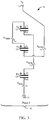
FIG. 1 is a schematic view of a Switched Capacitor Power Converter (SCPC), in accordance with an example embodiment of the present disclosure. -
FIG. 2 is a schematic view of the SCPC ofFIG. 1 during a first switching phase of a step-down conversion. -
FIG. 3 is a schematic view of the SCPC ofFIG. 1 during a second switching phase of a step-down conversion. -
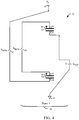
FIG. 4 is a schematic view of the SCPC ofFIG. 1 during a third switching phase of a step-down conversion. -
FIG. 5 is a schematic view of the SCPC ofFIG. 1 during a fourth switching phase of a step-down conversion. -
FIG. 6 is a schematic view of a state of the capacitors of the SCPC ofFIG. 1 during the four switching phases shown inFIG. 2 to FIG. 5 . -
FIG. 7 is a tabular view of the cumulative charging of the capacitors, input and output of the SCPC ofFIG. 1 during each of the four switching phases. -
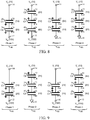
FIG. 8 is a schematic view of a state of the capacitors of the SCPC ofFIG. 1 during the four switching phases of a step-down conversion, in accordance with another example embodiment of the present disclosure. -
FIG. 9 is a schematic view of a state of the capacitors of the SCPC ofFIG. 1 during the four switching phases of a step-down conversion, in accordance with another example embodiment of the present disclosure. -
FIG. 10 is a flowchart representation of a method for multi-phase high conversion ratio switched capacitor power conversion in accordance with an example embodiment of the present disclosure. - Embodiments described herein provide for a novel SCPC topology with a wide conversion ratio using a four-phase conversion cycle with three floating capacitors. An SCPC requires several floating capacitors for a given conversion ratio (e.g., a ratio of an output voltage to the SCPC divided by an input voltage of the SCPC). The possible conversion ratios "M" of an SCPC, with "Nc" floating capacitors is given by the following equation (1), where "P" and "Q" are positive integers:

- In the case of a two phase SCPC topology, the number of capacitors can be especially limiting if their respective capacitive values are relatively large (e.g., several tens of nF). Large capacitors are often required to be implemented as discrete components, external to a monolithic integrated circuit (IC), thus undesirably increasing a pin count of the IC. In one example embodiment, the requirement for large capacitors is determined by the power level required to be converted by the SCPC.
- In one example of a two phase SCPC, with a conversion ratio of M=1/10 (e.g., the output voltage is 10 times lower than the input voltage), at least 5 floating capacitors are required, as determined by the Fibonacci limit. With more modern multi-phase SCPCs, this conversion ratio can be accomplished with 4 floating capacitors. With the novel 4-phase topology described herein, only 3 floating capacitors are required to provide comparable performance. In addition, the reduction of the number of floating capacitors to three also requires fewer component pins, thus resulting in a more compact solution in pin limited and/or component limited applications. The conversion ratio of M=1/10 is of particular utility as a secondary converter in a system operating from a 110V alternating mains, primarily stepped down to a 33V level, and then further converted to 3.3V with an SCPC for powering an IC. Furthermore, variants of the SCPC topology described herein, provide for increased granularity in multi-ratio SCPC based circuits.
-
FIG. 1 shows anexample embodiment 10 of an SCPC in accordance with the present disclosure. Theembodiment 10 converts an input voltage on aninput 12 to an output voltage on anoutput 14, wherein both the input voltage and the output voltage are referenced to a ground potential on aground 16. In one embodiment, the ground potential is zero volts, however this disclosure is adaptable to other ground potential values. Theembodiment 10 includes afirst capacitor 20, having a firsttop plate 22 and afirst bottom plate 24. Theembodiment 10 includes asecond capacitor 30, having a secondtop plate 32 and asecond bottom plate 34. Theembodiment 10 includes athird capacitor 40, having a thirdtop plate 42 and athird bottom plate 44. - The
embodiment 10 includes a plurality of switches to transfer charge, (and thus convert the input voltage to the output voltage), between theinput 12 theoutput 14. This charge transfer occurs by sequentially configuring connections between two or more of the threecapacitors first capacitor 20. - An
S1pvin switch 50 is connected between theinput 12 and the firsttop plate 22. AnS2pln switch 52 is connected between thefirst bottom plate 24 and a secondtop plate 32. AnS3p2n switch 54 is connected between thesecond bottom plate 34 and the thirdtop plate 42. AnS3nG switch 56 is connected between thethird bottom plate 44 and theground 16. AnS1p2p switch 60 is connected between the firsttop plate 22 and the secondtop plate 32. AnS2nG switch 62 is connected between thesecond bottom plate 34 and theground 16. AnS3plp switch 64 is connected between the firsttop plate 22 the thirdtop plate 42. An S3nvoswitch 66 is connected between theoutput 14 and thethird bottom plate 44. An S1nvoswitch 70 is connected between theoutput 14 and thefirst bottom plate 24. AnS1n3p switch 72 is connected between thefirst bottom plate 24 and the thirdtop plate 42. An S2nvoswitch 74 is connected between theoutput 14 and thesecond bottom plate 34. AnS1nG switch 76 is connected between thefirst bottom plate 24 and theground 16. -
FIG. 2 to FIG. 4 , with on-going reference toFIG. 1 show the switch connections for each of the four phases to implement an SCPC configured to down-convert an input voltage of (e.g. 10V) by a factor of one tenth to form an output voltage (e.g. 1V).FIG. 2 shows a connectivity of theembodiment 10 ofFIG. 1 for the first phase 80 (e.g., phase 1). Specifically, theoutput 14 is connected with theS1nVo switch 70 to thefirst bottom plate 24. The firsttop plate 22 is connected with theswitch S1p2p 60 to the secondtop plate 32. Thesecond bottom plate 34 is connected with theS2nG switch 62 to theground 16. -
FIG. 3 shows the connectivity of theembodiment 10 ofFIG. 1 for the second phase 82 (e.g., phase 2). Specifically, theoutput 14 is connected with theS2nVo switch 74 to thesecond bottom plate 34. The secondtop plate 32 is connected with theswitch S1p2p 60 to the firsttop plate 22. Thefirst bottom plate 24 is connected with theS1n3p switch 72 to the thirdtop plate 42. Thethird bottom plate 44 is connected with theS3nG switch 56 to theground 16. -
FIG. 4 shows a connectivity of theembodiment 10 ofFIG. 1 for the third phase 84 (e.g. phase 3). Specifically, theoutput 14 is connected with theS3nVo switch 66 to thethird bottom plate 44. The thirdtop plate 42 is connected with theS3plp switch 64 to the firsttop plate 22. Thefirst bottom plate 24 is connected with theS1nG switch 76 to theground 16. -
FIG. 5 shows the connectivity of theembodiment 10 ofFIG. 1 for the fourth phase 86 (e.g., phase 4). Specifically, theoutput 14 is connected with theS3nVo switch 66 to thethird bottom plate 44. The thirdtop plate 42 is connected with theswitch S3p2n 54 to thesecond bottom plate 34. The secondtop plate 32 is connected with theS2plp switch 52 to thefirst bottom plate 24. The firsttop plate 22 is connected with theSlpVin switch 50 to theinput 12. - It should be appreciated that the
embodiment 10 ofFIG. 1 is shown as a down-converter inFIG. 2 to FIG. 4 . In one embodiment, with reference to equation (1) above, the conversion ratio is 1/10 to covert the input of 10V to an output of 1V. By changing the order of the timing phases (e.g. phase 1,phase 2,phase 3 andphase 4 are replaced withphase 4,phase 3,phase 2 and phase 1), theembodiment 10 becomes an up-converter configured to convert the output voltage on theoutput 14 to an input voltage on theinput 12. In an example embodiment, each of the fourphases capacitors FIG. 1 is a secondary power converter preceded by a primary power converter, wherein the primary power converter is configured to convert a mains voltage (e.g. 110Vac) to an intermediate voltage (e.g. 33Vdc). The SCPC converts the intermediate voltage of 33Vdc to 3.3Vdc, suitable for powering an IC. -
FIG. 6 , with continued reference toFIG. 1 to FIG. 5 , further describes theexample embodiment 10 of a SCPC configured as a down-converter with a conversion ration of 1/10. During thefirst phase 80, theoutput 14 is connected to thefirst bottom plate 24. The firsttop plate 22 is connected to the secondtop plate 32. Thesecond bottom plate 34 is connected to theground 16. During thefirst phase 80, a charge "q1" (not shown) is transferred from theground 16 to theoutput 14. - During the
second phase 82, theoutput 14 is connected to thesecond bottom plate 34. The secondtop plate 32 is connected to the firsttop plate 22. Thefirst bottom plate 24 is connected to the thirdtop plate 42. Thethird bottom plate 44 is connected to theground 16. During thesecond phase 82, a charge "q2" (not shown) is transferred from theground 16 to theoutput 14. - During the
third phase 84, theoutput 14 is connected to thethird bottom plate 44. The thirdtop plate 42 is connected to the firsttop plate 22. Thefirst bottom plate 24 is connected to theground 16. During thethird phase 84, a charge "q3" (not shown) is transferred from theground 16 to theoutput 14. - During the
fourth phase 86, theoutput 14 is connected to thethird bottom plate 44. The thirdtop plate 42 is connected to thesecond bottom plate 34. The secondtop plate 32 is connected to thefirst bottom plate 24. The firsttop plate 22 is connected to theinput 12. During thefourth phase 86, a charge "q4" (not shown) is transferred from theinput 12 to theoutput 14. - For each of the four
phases capacitor FIG.6 , thefirst capacitor 20 maintains 3V across the firsttop plate 22 and thefirst bottom plate 24. Thesecond capacitor 30 maintains 4V across the secondtop plate 32 and thesecond bottom plate 34. Thethird capacitor 40 maintains 2V across the thirdtop plate 42 and thethird bottom plate 44. As shown byFIG. 6 , Kirchoff's Voltage Law is satisfied for each of the fourphases first phase 80, the voltage between theground 16 and the secondtop plate 32, (or the first top plate 22), is minus 4V. The voltage between the firsttop plate 22 and the first bottom plate is plus 3V. The voltage of theoutput 14 is plus IV, hence -4V+3V+1V=0V. - With reference to
FIG. 7 , and continued reference toFIG. 6 , the charge balance is also shown to be satisfied. More specifically, charge balance means that there is no net charge pumping or degradation of any of the threecapacitors phases FIG. 6 , for each capacitor and taking into account the polarity of each of the capacitor connections, one determines four equations with three unknowns. For a normalized analysis, we set q4 to 1 unit. For thefirst capacitor 20, the charge balance over the four respective phases is q1-q2-q3+q4=0. For example, during thefirst phase 80, q1 is positive because q1 flows from the firsttop plate 22 towards thefirst bottom plate 24. Conversely, during thesecond phase 82, q2 is negative because q2 flows from thefirst bottom plate 24 to the firsttop plate 22. Similar to the derivation for thefirst capacitor 20, the charge balance of thesecond capacitor 30 is given by -q1+q2+0+q4=0, and the charge balance of thethird capacitor 40 is given by 0-q2+q3+q4=0. Solving these four equations yields q4=1, q3=2, q2=3 and q1=4, as shown by the respective columns ofFIG. 7 defined by the fourphases capacitors yields 0 net charge difference between conversion cycles. Similarly,FIG. 7 shows a cumulated charge of 1 unit at theinput output 14. - Additional topologies are realizable compared to the step-down converter shown in
FIG. 1 to FIG. 6 . In one example, each topology is inverted from being a step-down converter to being a step-up converter. In other embodiments, for a conversion ratio of M=k/10, k is one of 3, 7 or 9. In other embodiments, for a conversion ratio of M=k/9, k is one of 1, 2, 4, 5, 7 or 8. Two variants of a step-down converter are shown inFIG. 8 and FIG. 9 , each having a conversion ratio (M) of 7/10, an input voltage of 10V and an output voltage of 7V. In one embodiment, a controller (not shown) controls theembodiment 10 ofFIG. 1 to generate the four timing phases and switching to dynamically adjust the conversion ratio. -
FIG. 8 , with continued reference toFIG. 1 , further describes theexample embodiment 10 of a SCPC configured as a down-converter with a conversion ration of 7/10. During thefirst phase 80, theoutput 14 is connected to thefirst bottom plate 24. The firsttop plate 22 is connected to thesecond bottom plate 34. The secondtop plate 32 is connected to theinput 12. - During the
second phase 82, theoutput 14 is connected to the secondtop plate 32. Thesecond bottom plate 34 is connected to the firsttop plate 22. Thefirst bottom plate 24 is connected to thethird bottom plate 44. The thirdtop plate 42 is connected to theinput 12. - During the
third phase 84, theoutput 14 is connected to the thirdtop plate 42. Thethird bottom plate 44 is connected to the firsttop plate 22. Thefirst bottom plate 24 is connected to theground 16. - During the
fourth phase 86, theoutput 14 is connected to thefirst bottom plate 24. The firsttop plate 22 is connected to the thirdtop plate 42. Thethird bottom plate 44 is connected to the secondtop plate 32. Thesecond bottom plate 34 is connected to theground 16. -
FIG. 9 , with continued reference toFIG. 1 , further describes theexample embodiment 10 of a SCPC configured as a down-converter with a conversion ration of 7/10. During thefirst phase 80, theoutput 14 is connected to thefirst bottom plate 24. The firsttop plate 22 is connected to thesecond bottom plate 34. The secondtop plate 32 is connected to theinput 12. - During the
second phase 82, theoutput 14 is connected to the secondtop plate 32. Thesecond bottom plate 34 is connected to the firsttop plate 22. Thefirst bottom plate 24 is connected to the thirdtop plate 42. Thethird bottom plate 44 is connected to theground 16. - During the
third phase 84, theoutput 14 is connected to thethird bottom plate 44. The thirdtop plate 42 is connected to the firsttop plate 22. Thefirst bottom plate 24 is connected to theinput 12. - During the
fourth phase 86, theoutput 14 is connected to thethird bottom plate 44. The thirdtop plate 42 is connected to the secondtop plate 32. Thesecond bottom plate 34 is connected to thefirst bottom plate 24. The firsttop plate 22 is connected to theinput 12. -
FIG. 10 shows amethod 90 for multi-phase power conversion with an SCPC having a high conversion ratio. At 92, four subcircuits (e.g., seeFIG. 2 to FIG. 5 ) are formed during arespective timing phase capacitors input 12, theoutput 14, aground 16, thebottom plate top plate top plate bottom plate - As will be appreciated, embodiments as disclosed include at least the following. In one embodiment, an apparatus comprises a first capacitor comprising a first top plate and a first bottom plate. A second capacitor comprises a second top plate and a second bottom plate. A third capacitor comprises a third top plate and a third bottom plate. An input comprises an input voltage. An output comprises an output voltage. A plurality of switches comprises an SlpVin switch connected between the input and the first top plate. An S2pln switch is connected between the first bottom plate and the second top plate. An S3p2n switch is connected between the second bottom plate and the third top plate. An S3nG switch is connected between the third bottom plate and a ground. An S1p2p switch is connected between the first top plate and the second top plate. An S2nG switch is connected between the second bottom plate and the ground. An S3plp switch is connected between the first top plate the third top plate. An S3nVo switch is connected between the output and the third bottom plate. An S1nVo switch is connected between the output and the first bottom plate. An S1n3p switch is connected between the first bottom plate and the third top plate. An S2nVo switch is connected between the output and the second bottom plate. An S1nG switch is connected between the first bottom plate and the ground.
- Alternative embodiments of the apparatus include one of the following features, or any combination thereof. During a first phase, the output is connected to the first bottom plate, the first top plate is connected to the second top plate and the second bottom plate is connected to the ground, during a second phase, the output is connected to the second bottom plate, the second top plate is connected to the first top plate, the first bottom plate is connected to the third top plate, and the third bottom plate is connected to the ground, during a third phase, the output is connected to the third bottom plate, the third top plate is connected to the first top plate and the first bottom plate is connected to the ground, and during a fourth phase, the output is connected to the third bottom plate, the third top plate is connected to the second bottom plate, the second top plate is connected to the first bottom plate, and the first top plate is connected to the input, wherein the output voltage is converted from the input voltage and the output voltage is one tenth of the input voltage. The third phase follows the fourth phase, the second phase follows the third phase, the first phase follows the second phase, wherein the input voltage is converted from the output voltage and the input voltage is ten times greater than the output voltage. During a first phase, the output is connected to the first bottom plate, the first top plate is connected to the second bottom plate and the second top plate is connected to the input, during a second phase, the output is connected to the second top plate, the second bottom plate is connected to the first top plate, the first bottom plate is connected to the third bottom plate, and the third top plate is connected to the input, during a third phase, the output is connected to the third top plate, the third bottom plate is connected to the first top plate and the first bottom plate is connected to the ground, and during a fourth phase, the output is connected to the first bottom plate, the first top plate is connected to the third top plate, the third bottom plate is connected to the second top plate, and the second bottom plate is connected to the ground, wherein the output voltage is converted from the input voltage and output voltage is seven tenths of the input voltage. During a first phase, the output is connected to the first bottom plate, the first top plate is connected to the second bottom plate and the second top plate is connected to the input, during a second phase, the output is connected to the second top plate, the second bottom plate is connected to the first top plate, the first bottom plate is connected to the third top plate, and the third bottom plate is connected to the ground, during a third phase, the output is connected to the third bottom plate, the third top plate is connected to the first top plate and the first bottom plate is connected to the input, and during a fourth phase, the output is connected to the third bottom plate, the third top plate is connected to the second top plate, the second bottom plate is connected to the first bottom plate, and the first top plate is connected to the input, wherein the output voltage is converted from the input voltage and the output voltage is seven tenths of the input voltage. The output voltage is converted from the input voltage with a conversion ratio defined by a numerator representing the output voltage and equal to one of 1, 3, 7 and 9, and a denominator representing the input voltage and equal to 10. The output voltage is converted from the input voltage with a conversion ratio defined by a numerator representing the output voltage and equal to one of 1, 2, 4, 5, 7 and 8, and a denominator representing the input voltage and equal to 9. A controller is configured to control a respective subset of the plurality of switches for each of four non-overlapping phases. Each of the plurality of switches is a field effect transistor. A gate of at least one of the plurality of switches is connected to a multiplexer configured to multiplex more than one timing phase signal from a controller.
- In another embodiment, a method for multi-phase high conversion ratio switched capacitor power conversion comprises sequentially forming one of four subcircuits during a respective timing phase, wherein each subcircuit comprises at most three capacitors. Conversions occurs between an input voltage of an input and an output voltage of an output, by sequentially connecting for each respective timing phase, one of the input, the output, a ground, a top plate of a first one of the three capacitors and a bottom plate of the first one of the three capacitors to one of a top plate of a second one of the three capacitors and a bottom plate of the second one of the three capacitors.
- Alternative embodiments of the method for multi-phase high conversion ratio switched capacitor power conversion include one of the following features, or any combination thereof. The input voltage is converted to the output voltage, wherein the first subcircuit is formed with a first timing phase, the second subcircuit is formed with a second timing phase, the third subcircuit is formed with a third timing phase and the fourth subcircuit is formed with a fourth timing phase. The output voltage is converted to the input voltage, wherein the first subcircuit is formed with a fourth timing phase, the second subcircuit is formed with a third timing phase, the third subcircuit is formed with a second timing phase and the fourth subcircuit is formed with a first timing phase. The input voltage is converted to the output voltage with a conversion ratio defined by a numerator representing the output voltage and equal to one of 1, 3, 7 and 9, and a denominator representing the input voltage and equal to 10. The input voltage is converted to the output voltage with a conversion ratio defined by a numerator representing the output voltage and equal to one of 1, 2, 4, 5, 7 and 8, and a denominator representing the input voltage and equal to 9. Each of the respective timing phases is generated with a controller.
- In another embodiment, a system comprises three capacitors. An input comprises an input voltage. An output comprises an output voltage converted from the input voltage. A controller is configured to sequentially form each of four subcircuits during a respective nonoverlapping timing phase, wherein each of the four subcircuits comprises one of a top plate of a first one of the three capacitors and a bottom plate of the first one of the three capacitors switchably connected to one of the input, the output, a ground, a top plate of a second one of the three capacitors and a bottom plate of the second one of the three capacitors.
- Alternative embodiments of the system include one of the following features, or any combination thereof. The system is a secondary switched capacitor power converter connected between a primary power converter configured to convert a mains voltage to the input voltage. The controller is configured to switchably connect two of the three capacitors together during a first timing phase and a third timing phase, and to switchably connect three of the three capacitors together during a second timing phase and a fourth timing phase. The controller is programmable and configured to switchably connect at least two of the three capacitors in each of four nonoverlapping timing phases to achieve one of a plurality of conversion ratios defined by the output voltage divided by the input voltage.
- Although the invention is described herein with reference to specific embodiments, various modifications and changes can be made without departing from the scope of the present invention as set forth in the claims below. Accordingly, the specification and figures are to be regarded in an illustrative rather than a restrictive sense, and all such modifications are intended to be included within the scope of the present invention. Any benefits, advantages, or solutions to problems that are described herein with regard to specific embodiments are not intended to be construed as a critical, required, or essential feature or element of any or all the claims.
- Unless stated otherwise, terms such as "first" and "second" are used to arbitrarily distinguish between the elements such terms describe. Thus, these terms are not necessarily intended to indicate temporal or other prioritization of such elements.
Claims (15)
- An apparatus comprising:a first capacitor comprising a first top plate and a first bottom plate;a second capacitor comprising a second top plate and a second bottom plate;a third capacitor comprising a third top plate and a third bottom plate;an input comprising an input voltage;an output comprising an output voltage; anda plurality of switches comprising an SlpVin switch connected between the input and the first top plate, an S2pln switch connected between the first bottom plate and the second top plate, an S3p2n switch connected between the second bottom plate and the third top plate, an S3nG switch connected between the third bottom plate and a ground, an S1p2p switch connected between the first top plate and the second top plate, an S2nG switch connected between the second bottom plate and the ground, an S3plp switch connected between the first top plate the third top plate, an S3nVo switch connected between the output and the third bottom plate, an S1nVo switch connected between the output and the first bottom plate, an S1n3p switch connected between the first bottom plate and the third top plate, an S2nVo switch connected between the output and the second bottom plate, and an S1nG switch connected between the first bottom plate and the ground.
- The apparatus of claim 1 wherein:during a first phase, the output is connected to the first bottom plate, the first top plate is connected to the second top plate and the second bottom plate is connected to the ground,during a second phase, the output is connected to the second bottom plate, the second top plate is connected to the first top plate, the first bottom plate is connected to the third top plate, and the third bottom plate is connected to the ground,during a third phase, the output is connected to the third bottom plate, the third top plate is connected to the first top plate and the first bottom plate is connected to the ground, andduring a fourth phase, the output is connected to the third bottom plate, the third top plate is connected to the second bottom plate, the second top plate is connected to the first bottom plate, and the first top plate is connected to the input, wherein the output voltage is converted from the input voltage and the output voltage is one tenth of the input voltage.
- The apparatus of claim 2 wherein the third phase follows the fourth phase, the second phase follows the third phase, the first phase follows the second phase, wherein the input voltage is converted from the output voltage and the input voltage is ten times greater than the output voltage.
- The apparatus of any preceding claim wherein:during a first phase, the output is connected to the first bottom plate, the first top plate is connected to the second bottom plate and the second top plate is connected to the input,during a second phase, the output is connected to the second top plate, the second bottom plate is connected to the first top plate, the first bottom plate is connected to the third bottom plate, and the third top plate is connected to the input,during a third phase, the output is connected to the third top plate, the third bottom plate is connected to the first top plate and the first bottom plate is connected to the ground, andduring a fourth phase, the output is connected to the first bottom plate, the first top plate is connected to the third top plate, the third bottom plate is connected to the second top plate, and the second bottom plate is connected to the ground, wherein the output voltage is converted from the input voltage and output voltage is seven tenths of the input voltage.
- The apparatus of any preceding claim wherein:during a first phase, the output is connected to the first bottom plate, the first top plate is connected to the second bottom plate and the second top plate is connected to the input,during a second phase, the output is connected to the second top plate, the second bottom plate is connected to the first top plate, the first bottom plate is connected to the third top plate, and the third bottom plate is connected to the ground,during a third phase, the output is connected to the third bottom plate, the third top plate is connected to the first top plate and the first bottom plate is connected to the input, andduring a fourth phase, the output is connected to the third bottom plate, the third top plate is connected to the second top plate, the second bottom plate is connected to the first bottom plate, and the first top plate is connected to the input, wherein the output voltage is converted from the input voltage and the output voltage is seven tenths of the input voltage.
- The apparatus of any preceding claim wherein the output voltage is converted from the input voltage with a conversion ratio defined by a numerator representing the output voltage and equal to one of 1, 3, 7 and 9, and a denominator representing the input voltage and equal to 10.
- The apparatus of any preceding claim wherein the output voltage is converted from the input voltage with a conversion ratio defined by a numerator representing the output voltage and equal to one of 1, 2, 4, 5, 7 and 8, and a denominator representing the input voltage and equal to 9.
- The apparatus of any preceding claim further comprising a controller configured to control a respective subset of the plurality of switches for each of four non-overlapping phases.
- The apparatus of any preceding claim wherein each of the plurality of switches is a field effect transistor.
- The apparatus of any preceding claim wherein a gate of at least one of the plurality of switches is connected to a multiplexer configured to multiplex more than one timing phase signal from a controller.
- A method for multi-phase high conversion ratio switched capacitor power conversion comprising:sequentially forming one of four subcircuits during a respective timing phase, wherein each subcircuit comprises at most three capacitors; andconverting between an input voltage of an input and an output voltage of an output, by sequentially connecting for each respective timing phase, one of the input, the output, a ground, a top plate of a first one of the three capacitors and a bottom plate of the first one of the three capacitors to one of a top plate of a second one of the three capacitors and a bottom plate of the second one of the three capacitors.
- The method of claim 11 wherein the input voltage is converted to the output voltage, wherein the first subcircuit is formed with a first timing phase, the second subcircuit is formed with a second timing phase, the third subcircuit is formed with a third timing phase and the fourth subcircuit is formed with a fourth timing phase.
- The method of claim 11 or 12 wherein the output voltage is converted to the input voltage, wherein the first subcircuit is formed with a fourth timing phase, the second subcircuit is formed with a third timing phase, the third subcircuit is formed with a second timing phase and the fourth subcircuit is formed with a first timing phase.
- The method of any of claims 11 to 13 further comprising converting the input voltage to the output voltage with a conversion ratio defined by a numerator representing the output voltage and equal to one of 1, 3, 7 and 9, and a denominator representing the input voltage and equal to 10.
- The method of any of claims 11 to 14 further comprising converting the input voltage to the output voltage with a conversion ratio defined by a numerator representing the output voltage and equal to one of 1, 2, 4, 5, 7 and 8, and a denominator representing the input voltage and equal to 9.
Applications Claiming Priority (1)
| Application Number | Priority Date | Filing Date | Title |
|---|---|---|---|
| US16/527,693 US10958161B2 (en) | 2019-07-31 | 2019-07-31 | Multi-phase high conversion ratio switched capacitor power converter |
Publications (2)
| Publication Number | Publication Date |
|---|---|
| EP3772167A1 true EP3772167A1 (en) | 2021-02-03 |
| EP3772167B1 EP3772167B1 (en) | 2025-06-25 |
Family
ID=71620193
Family Applications (1)
| Application Number | Title | Priority Date | Filing Date |
|---|---|---|---|
| EP20185787.7A Active EP3772167B1 (en) | 2019-07-31 | 2020-07-14 | Multi-phase high conversion ratio switched capacitor power converter |
Country Status (3)
| Country | Link |
|---|---|
| US (1) | US10958161B2 (en) |
| EP (1) | EP3772167B1 (en) |
| CN (1) | CN112311224B (en) |
Citations (3)
| Publication number | Priority date | Publication date | Assignee | Title |
|---|---|---|---|---|
| WO2009136368A1 (en) * | 2008-05-09 | 2009-11-12 | Nxp B.V. | Charge pump dc-dc converter |
| CN104410271A (en) * | 2014-12-17 | 2015-03-11 | 南京航空航天大学 | Multiphase interleaving technology for five-conversion-ratio charge pump by using three flying capacitors |
| WO2016138361A1 (en) * | 2015-02-27 | 2016-09-01 | President And Fellows Of Harvard College | Device and method for hybrid feedback control of a switch-capacitor multi-unit voltage regulator |
Family Cites Families (6)
| Publication number | Priority date | Publication date | Assignee | Title |
|---|---|---|---|---|
| FR2852748B1 (en) * | 2003-03-18 | 2005-06-03 | SYNCHRONOUS SWITCHING SERVER HOPPER AND LOW LOSSES | |
| DE102008056748A1 (en) * | 2008-11-11 | 2010-05-20 | Austriamicrosystems Ag | voltage converter |
| US8159091B2 (en) * | 2009-04-01 | 2012-04-17 | Chimei Innolux Corporation | Switch circuit of DC/DC converter configured to conduct various modes for charging/discharging |
| EP2846448B1 (en) | 2013-09-06 | 2018-11-14 | Nxp B.V. | Switched capacitor power converter |
| EP3396834B1 (en) * | 2017-04-28 | 2023-03-22 | Nxp B.V. | Switched capacitor power converter |
| US20190393782A1 (en) * | 2018-06-25 | 2019-12-26 | Mykhaylo Teplechuk | Combined inductive and switched capacitive power supply conversion |
-
2019
- 2019-07-31 US US16/527,693 patent/US10958161B2/en active Active
-
2020
- 2020-07-14 EP EP20185787.7A patent/EP3772167B1/en active Active
- 2020-07-28 CN CN202010741064.2A patent/CN112311224B/en active Active
Patent Citations (3)
| Publication number | Priority date | Publication date | Assignee | Title |
|---|---|---|---|---|
| WO2009136368A1 (en) * | 2008-05-09 | 2009-11-12 | Nxp B.V. | Charge pump dc-dc converter |
| CN104410271A (en) * | 2014-12-17 | 2015-03-11 | 南京航空航天大学 | Multiphase interleaving technology for five-conversion-ratio charge pump by using three flying capacitors |
| WO2016138361A1 (en) * | 2015-02-27 | 2016-09-01 | President And Fellows Of Harvard College | Device and method for hybrid feedback control of a switch-capacitor multi-unit voltage regulator |
Non-Patent Citations (1)
| Title |
|---|
| LARSEN DENNIS OLAND ET AL: "Dynamically Reconfigurable Gearbox Switched-Capacitor DC-DC Converter", 2018 IEEE NORDIC CIRCUITS AND SYSTEMS CONFERENCE (NORCAS): NORCHIP AND INTERNATIONAL SYMPOSIUM OF SYSTEM-ON-CHIP (SOC), IEEE, 30 October 2018 (2018-10-30), pages 1 - 5, XP033471595, DOI: 10.1109/NORCHIP.2018.8573520 * |
Also Published As
| Publication number | Publication date |
|---|---|
| US10958161B2 (en) | 2021-03-23 |
| EP3772167B1 (en) | 2025-06-25 |
| US20210036603A1 (en) | 2021-02-04 |
| CN112311224B (en) | 2025-12-02 |
| CN112311224A (en) | 2021-02-02 |
Similar Documents
| Publication | Publication Date | Title |
|---|---|---|
| US10574140B2 (en) | Charge balanced charge pump control | |
| US6198645B1 (en) | Buck and boost switched capacitor gain stage with optional shared rest state | |
| US10069408B2 (en) | Switched capacitor circuit modifying voltage on the inductor of a buck regulator | |
| US11936290B2 (en) | Switched capacitor converter and control method | |
| Zhu et al. | Switched-capacitor power supplies: DC voltage ratio, efficiency, ripple, regulation | |
| JP6685282B2 (en) | Shared bootstrap capacitor for multi-phase buck converter circuit and method | |
| US20150015225A1 (en) | Multi-phase buck dc converter | |
| US20040245972A1 (en) | Series chopper with synchronous switching | |
| EP2849323A1 (en) | Control circuit for multiple high side switches | |
| CN101990736A (en) | Adaptive Gain Boost/Buck Switched Capacitor DC/DC Converter | |
| US9570976B2 (en) | Switched capacitor power converter | |
| EP3355459A1 (en) | Voltage converter and method for voltage conversion | |
| Chen et al. | Dual-path hybrid Dickson converter for high-ratio conversions in point-of-load applications | |
| TWI504118B (en) | Dc-dc converter and method thereof | |
| CN107742978B (en) | Charge pump circuit with enhancing driving capability | |
| US9383761B2 (en) | Apparatus and method for multiphase SMPS interleaving | |
| JPH08205524A (en) | Voltage converter | |
| WO2010023595A1 (en) | Voltage converter | |
| US9780637B2 (en) | Buck converter with changeable relationship between output voltage and duty cycle, and buck converting apparatus using the same | |
| TW201828580A (en) | Switched capacitor dc-dc convertor circuit and generating method thereof | |
| EP3772167B1 (en) | Multi-phase high conversion ratio switched capacitor power converter | |
| Saif et al. | Comparison of charge pump and boost circuits for high voltage & low power voltage conversions | |
| Hua et al. | An auto-reconfigurable dual-output SC DC-DC regulator with sub-harmonic fixed on-time control for energy-harvesting applications | |
| Keramida et al. | A reconfigurable Buck-boost cross-coupled charge pump | |
| Terada et al. | Switched-capacitor (SC) DC-DC converter with fine tune control outputs |
Legal Events
| Date | Code | Title | Description |
|---|---|---|---|
| PUAI | Public reference made under article 153(3) epc to a published international application that has entered the european phase |
Free format text: ORIGINAL CODE: 0009012 |
|
| STAA | Information on the status of an ep patent application or granted ep patent |
Free format text: STATUS: THE APPLICATION HAS BEEN PUBLISHED |
|
| AK | Designated contracting states |
Kind code of ref document: A1 Designated state(s): AL AT BE BG CH CY CZ DE DK EE ES FI FR GB GR HR HU IE IS IT LI LT LU LV MC MK MT NL NO PL PT RO RS SE SI SK SM TR |
|
| AX | Request for extension of the european patent |
Extension state: BA ME |
|
| STAA | Information on the status of an ep patent application or granted ep patent |
Free format text: STATUS: REQUEST FOR EXAMINATION WAS MADE |
|
| 17P | Request for examination filed |
Effective date: 20210803 |
|
| RBV | Designated contracting states (corrected) |
Designated state(s): AL AT BE BG CH CY CZ DE DK EE ES FI FR GB GR HR HU IE IS IT LI LT LU LV MC MK MT NL NO PL PT RO RS SE SI SK SM TR |
|
| STAA | Information on the status of an ep patent application or granted ep patent |
Free format text: STATUS: EXAMINATION IS IN PROGRESS |
|
| 17Q | First examination report despatched |
Effective date: 20221212 |
|
| GRAP | Despatch of communication of intention to grant a patent |
Free format text: ORIGINAL CODE: EPIDOSNIGR1 |
|
| STAA | Information on the status of an ep patent application or granted ep patent |
Free format text: STATUS: GRANT OF PATENT IS INTENDED |
|
| INTG | Intention to grant announced |
Effective date: 20250313 |
|
| GRAS | Grant fee paid |
Free format text: ORIGINAL CODE: EPIDOSNIGR3 |
|
| GRAA | (expected) grant |
Free format text: ORIGINAL CODE: 0009210 |
|
| STAA | Information on the status of an ep patent application or granted ep patent |
Free format text: STATUS: THE PATENT HAS BEEN GRANTED |
|
| AK | Designated contracting states |
Kind code of ref document: B1 Designated state(s): AL AT BE BG CH CY CZ DE DK EE ES FI FR GB GR HR HU IE IS IT LI LT LU LV MC MK MT NL NO PL PT RO RS SE SI SK SM TR |
|
| REG | Reference to a national code |
Ref country code: GB Ref legal event code: FG4D |
|
| REG | Reference to a national code |
Ref country code: CH Ref legal event code: EP |
|
| REG | Reference to a national code |
Ref country code: CH Ref legal event code: EP |
|
| REG | Reference to a national code |
Ref country code: IE Ref legal event code: FG4D |
|
| REG | Reference to a national code |
Ref country code: DE Ref legal event code: R096 Ref document number: 602020053192 Country of ref document: DE |
|
| PG25 | Lapsed in a contracting state [announced via postgrant information from national office to epo] |
Ref country code: FI Free format text: LAPSE BECAUSE OF FAILURE TO SUBMIT A TRANSLATION OF THE DESCRIPTION OR TO PAY THE FEE WITHIN THE PRESCRIBED TIME-LIMIT Effective date: 20250625 |
|
| PGFP | Annual fee paid to national office [announced via postgrant information from national office to epo] |
Ref country code: DE Payment date: 20250724 Year of fee payment: 6 |
|
| REG | Reference to a national code |
Ref country code: LT Ref legal event code: MG9D |
|
| PG25 | Lapsed in a contracting state [announced via postgrant information from national office to epo] |
Ref country code: GR Free format text: LAPSE BECAUSE OF FAILURE TO SUBMIT A TRANSLATION OF THE DESCRIPTION OR TO PAY THE FEE WITHIN THE PRESCRIBED TIME-LIMIT Effective date: 20250926 Ref country code: NO Free format text: LAPSE BECAUSE OF FAILURE TO SUBMIT A TRANSLATION OF THE DESCRIPTION OR TO PAY THE FEE WITHIN THE PRESCRIBED TIME-LIMIT Effective date: 20250925 |
|
| PG25 | Lapsed in a contracting state [announced via postgrant information from national office to epo] |
Ref country code: BG Free format text: LAPSE BECAUSE OF FAILURE TO SUBMIT A TRANSLATION OF THE DESCRIPTION OR TO PAY THE FEE WITHIN THE PRESCRIBED TIME-LIMIT Effective date: 20250625 |
|
| PG25 | Lapsed in a contracting state [announced via postgrant information from national office to epo] |
Ref country code: HR Free format text: LAPSE BECAUSE OF FAILURE TO SUBMIT A TRANSLATION OF THE DESCRIPTION OR TO PAY THE FEE WITHIN THE PRESCRIBED TIME-LIMIT Effective date: 20250625 |
|
| PG25 | Lapsed in a contracting state [announced via postgrant information from national office to epo] |
Ref country code: RS Free format text: LAPSE BECAUSE OF FAILURE TO SUBMIT A TRANSLATION OF THE DESCRIPTION OR TO PAY THE FEE WITHIN THE PRESCRIBED TIME-LIMIT Effective date: 20250925 |
|
| PG25 | Lapsed in a contracting state [announced via postgrant information from national office to epo] |
Ref country code: LV Free format text: LAPSE BECAUSE OF FAILURE TO SUBMIT A TRANSLATION OF THE DESCRIPTION OR TO PAY THE FEE WITHIN THE PRESCRIBED TIME-LIMIT Effective date: 20250625 |
|
| REG | Reference to a national code |
Ref country code: NL Ref legal event code: MP Effective date: 20250625 |
|
| PG25 | Lapsed in a contracting state [announced via postgrant information from national office to epo] |
Ref country code: NL Free format text: LAPSE BECAUSE OF FAILURE TO SUBMIT A TRANSLATION OF THE DESCRIPTION OR TO PAY THE FEE WITHIN THE PRESCRIBED TIME-LIMIT Effective date: 20250625 |
|
| PG25 | Lapsed in a contracting state [announced via postgrant information from national office to epo] |
Ref country code: PT Free format text: LAPSE BECAUSE OF FAILURE TO SUBMIT A TRANSLATION OF THE DESCRIPTION OR TO PAY THE FEE WITHIN THE PRESCRIBED TIME-LIMIT Effective date: 20251027 |
|
| REG | Reference to a national code |
Ref country code: AT Ref legal event code: MK05 Ref document number: 1807642 Country of ref document: AT Kind code of ref document: T Effective date: 20250625 |
|
| PG25 | Lapsed in a contracting state [announced via postgrant information from national office to epo] |
Ref country code: IS Free format text: LAPSE BECAUSE OF FAILURE TO SUBMIT A TRANSLATION OF THE DESCRIPTION OR TO PAY THE FEE WITHIN THE PRESCRIBED TIME-LIMIT Effective date: 20251025 |
|
| PG25 | Lapsed in a contracting state [announced via postgrant information from national office to epo] |
Ref country code: AT Free format text: LAPSE BECAUSE OF FAILURE TO SUBMIT A TRANSLATION OF THE DESCRIPTION OR TO PAY THE FEE WITHIN THE PRESCRIBED TIME-LIMIT Effective date: 20250625 Ref country code: SM Free format text: LAPSE BECAUSE OF FAILURE TO SUBMIT A TRANSLATION OF THE DESCRIPTION OR TO PAY THE FEE WITHIN THE PRESCRIBED TIME-LIMIT Effective date: 20250625 |
|
| PG25 | Lapsed in a contracting state [announced via postgrant information from national office to epo] |
Ref country code: CZ Free format text: LAPSE BECAUSE OF FAILURE TO SUBMIT A TRANSLATION OF THE DESCRIPTION OR TO PAY THE FEE WITHIN THE PRESCRIBED TIME-LIMIT Effective date: 20250625 |
|
| PG25 | Lapsed in a contracting state [announced via postgrant information from national office to epo] |
Ref country code: PL Free format text: LAPSE BECAUSE OF FAILURE TO SUBMIT A TRANSLATION OF THE DESCRIPTION OR TO PAY THE FEE WITHIN THE PRESCRIBED TIME-LIMIT Effective date: 20250625 |
|
| PG25 | Lapsed in a contracting state [announced via postgrant information from national office to epo] |
Ref country code: EE Free format text: LAPSE BECAUSE OF FAILURE TO SUBMIT A TRANSLATION OF THE DESCRIPTION OR TO PAY THE FEE WITHIN THE PRESCRIBED TIME-LIMIT Effective date: 20250625 |
|
| PG25 | Lapsed in a contracting state [announced via postgrant information from national office to epo] |
Ref country code: SK Free format text: LAPSE BECAUSE OF FAILURE TO SUBMIT A TRANSLATION OF THE DESCRIPTION OR TO PAY THE FEE WITHIN THE PRESCRIBED TIME-LIMIT Effective date: 20250625 |
|
| PG25 | Lapsed in a contracting state [announced via postgrant information from national office to epo] |
Ref country code: ES Free format text: LAPSE BECAUSE OF FAILURE TO SUBMIT A TRANSLATION OF THE DESCRIPTION OR TO PAY THE FEE WITHIN THE PRESCRIBED TIME-LIMIT Effective date: 20250625 |
|
| REG | Reference to a national code |
Ref country code: CH Ref legal event code: H13 Free format text: ST27 STATUS EVENT CODE: U-0-0-H10-H13 (AS PROVIDED BY THE NATIONAL OFFICE) Effective date: 20260224 |
|
| PG25 | Lapsed in a contracting state [announced via postgrant information from national office to epo] |
Ref country code: LU Free format text: LAPSE BECAUSE OF NON-PAYMENT OF DUE FEES Effective date: 20250714 Ref country code: RO Free format text: LAPSE BECAUSE OF FAILURE TO SUBMIT A TRANSLATION OF THE DESCRIPTION OR TO PAY THE FEE WITHIN THE PRESCRIBED TIME-LIMIT Effective date: 20250625 |
|
| REG | Reference to a national code |
Ref country code: BE Ref legal event code: MM Effective date: 20250731 Ref country code: DE Ref legal event code: R097 Ref document number: 602020053192 Country of ref document: DE |
|
| PG25 | Lapsed in a contracting state [announced via postgrant information from national office to epo] |
Ref country code: MC Free format text: LAPSE BECAUSE OF FAILURE TO SUBMIT A TRANSLATION OF THE DESCRIPTION OR TO PAY THE FEE WITHIN THE PRESCRIBED TIME-LIMIT Effective date: 20250625 |
|
| PG25 | Lapsed in a contracting state [announced via postgrant information from national office to epo] |
Ref country code: DK Free format text: LAPSE BECAUSE OF FAILURE TO SUBMIT A TRANSLATION OF THE DESCRIPTION OR TO PAY THE FEE WITHIN THE PRESCRIBED TIME-LIMIT Effective date: 20250625 |
|
| PG25 | Lapsed in a contracting state [announced via postgrant information from national office to epo] |
Ref country code: BE Free format text: LAPSE BECAUSE OF NON-PAYMENT OF DUE FEES Effective date: 20250731 Ref country code: IT Free format text: LAPSE BECAUSE OF FAILURE TO SUBMIT A TRANSLATION OF THE DESCRIPTION OR TO PAY THE FEE WITHIN THE PRESCRIBED TIME-LIMIT Effective date: 20250625 |
|
| PG25 | Lapsed in a contracting state [announced via postgrant information from national office to epo] |
Ref country code: CH Free format text: LAPSE BECAUSE OF NON-PAYMENT OF DUE FEES Effective date: 20250731 |
|
| PLBE | No opposition filed within time limit |
Free format text: ORIGINAL CODE: 0009261 |
|
| STAA | Information on the status of an ep patent application or granted ep patent |
Free format text: STATUS: NO OPPOSITION FILED WITHIN TIME LIMIT |
|
| REG | Reference to a national code |
Ref country code: CH Ref legal event code: L10 Free format text: ST27 STATUS EVENT CODE: U-0-0-L10-L00 (AS PROVIDED BY THE NATIONAL OFFICE) Effective date: 20260507 |
|
| 26N | No opposition filed |
Effective date: 20260326 |
|
| PG25 | Lapsed in a contracting state [announced via postgrant information from national office to epo] |
Ref country code: LT Free format text: LAPSE BECAUSE OF FAILURE TO SUBMIT A TRANSLATION OF THE DESCRIPTION OR TO PAY THE FEE WITHIN THE PRESCRIBED TIME-LIMIT Effective date: 20250625 |
|
| PGFP | Annual fee paid to national office [announced via postgrant information from national office to epo] |
Ref country code: GB Payment date: 20260618 Year of fee payment: 7 |
|
| PG25 | Lapsed in a contracting state [announced via postgrant information from national office to epo] |
Ref country code: IE Free format text: LAPSE BECAUSE OF NON-PAYMENT OF DUE FEES Effective date: 20250714 |
|
| PGFP | Annual fee paid to national office [announced via postgrant information from national office to epo] |
Ref country code: FR Payment date: 20260619 Year of fee payment: 7 |
|
| PG25 | Lapsed in a contracting state [announced via postgrant information from national office to epo] |
Ref country code: CY Free format text: LAPSE BECAUSE OF FAILURE TO SUBMIT A TRANSLATION OF THE DESCRIPTION OR TO PAY THE FEE WITHIN THE PRESCRIBED TIME-LIMIT Effective date: 20250625 Ref country code: SE Free format text: LAPSE BECAUSE OF FAILURE TO SUBMIT A TRANSLATION OF THE DESCRIPTION OR TO PAY THE FEE WITHIN THE PRESCRIBED TIME-LIMIT Effective date: 20250625 |