EP3772100A1 - Semiconductor package structure including antenna - Google Patents
Semiconductor package structure including antenna Download PDFInfo
- Publication number
- EP3772100A1 EP3772100A1 EP20185395.9A EP20185395A EP3772100A1 EP 3772100 A1 EP3772100 A1 EP 3772100A1 EP 20185395 A EP20185395 A EP 20185395A EP 3772100 A1 EP3772100 A1 EP 3772100A1
- Authority
- EP
- European Patent Office
- Prior art keywords
- semiconductor package
- electrical connectors
- semiconductor die
- rdl
- semiconductor
- Prior art date
- Legal status (The legal status is an assumption and is not a legal conclusion. Google has not performed a legal analysis and makes no representation as to the accuracy of the status listed.)
- Granted
Links
Images


Classifications
-
- H—ELECTRICITY
- H10—SEMICONDUCTOR DEVICES; ELECTRIC SOLID-STATE DEVICES NOT OTHERWISE PROVIDED FOR
- H10W—GENERIC PACKAGES, INTERCONNECTIONS, CONNECTORS OR OTHER CONSTRUCTIONAL DETAILS OF DEVICES COVERED BY CLASS H10
- H10W90/00—Package configurations
-
- H—ELECTRICITY
- H01—ELECTRIC ELEMENTS
- H01Q—ANTENNAS, i.e. RADIO AERIALS
- H01Q1/00—Details of, or arrangements associated with, antennas
- H01Q1/12—Supports; Mounting means
- H01Q1/22—Supports; Mounting means by structural association with other equipment or articles
- H01Q1/2283—Supports; Mounting means by structural association with other equipment or articles mounted in or on the surface of a semiconductor substrate as a chip-type antenna or integrated with other components into an IC package
-
- H—ELECTRICITY
- H01—ELECTRIC ELEMENTS
- H01Q—ANTENNAS, i.e. RADIO AERIALS
- H01Q1/00—Details of, or arrangements associated with, antennas
- H01Q1/36—Structural form of radiating elements, e.g. cone, spiral, umbrella; Particular materials used therewith
- H01Q1/38—Structural form of radiating elements, e.g. cone, spiral, umbrella; Particular materials used therewith formed by a conductive layer on an insulating support
-
- H—ELECTRICITY
- H05—ELECTRIC TECHNIQUES NOT OTHERWISE PROVIDED FOR
- H05K—PRINTED CIRCUITS; CASINGS OR CONSTRUCTIONAL DETAILS OF ELECTRIC APPARATUS; MANUFACTURE OF ASSEMBLAGES OF ELECTRICAL COMPONENTS
- H05K1/00—Printed circuits
- H05K1/16—Printed circuits incorporating printed electric components, e.g. printed resistors, capacitors or inductors
- H05K1/165—Printed circuits incorporating printed electric components, e.g. printed resistors, capacitors or inductors incorporating printed inductors
-
- H—ELECTRICITY
- H05—ELECTRIC TECHNIQUES NOT OTHERWISE PROVIDED FOR
- H05K—PRINTED CIRCUITS; CASINGS OR CONSTRUCTIONAL DETAILS OF ELECTRIC APPARATUS; MANUFACTURE OF ASSEMBLAGES OF ELECTRICAL COMPONENTS
- H05K1/00—Printed circuits
- H05K1/18—Printed circuits structurally associated with non-printed electric components
- H05K1/181—Printed circuits structurally associated with non-printed electric components associated with surface mounted components
-
- H—ELECTRICITY
- H10—SEMICONDUCTOR DEVICES; ELECTRIC SOLID-STATE DEVICES NOT OTHERWISE PROVIDED FOR
- H10W—GENERIC PACKAGES, INTERCONNECTIONS, CONNECTORS OR OTHER CONSTRUCTIONAL DETAILS OF DEVICES COVERED BY CLASS H10
- H10W44/00—Electrical arrangements for controlling or matching impedance
- H10W44/20—Electrical arrangements for controlling or matching impedance at high-frequency [HF] or radio frequency [RF]
-
- H—ELECTRICITY
- H10—SEMICONDUCTOR DEVICES; ELECTRIC SOLID-STATE DEVICES NOT OTHERWISE PROVIDED FOR
- H10W—GENERIC PACKAGES, INTERCONNECTIONS, CONNECTORS OR OTHER CONSTRUCTIONAL DETAILS OF DEVICES COVERED BY CLASS H10
- H10W70/00—Package substrates; Interposers; Redistribution layers [RDL]
- H10W70/60—Insulating or insulated package substrates; Interposers; Redistribution layers
- H10W70/611—Insulating or insulated package substrates; Interposers; Redistribution layers for connecting multiple chips together
-
- H—ELECTRICITY
- H10—SEMICONDUCTOR DEVICES; ELECTRIC SOLID-STATE DEVICES NOT OTHERWISE PROVIDED FOR
- H10W—GENERIC PACKAGES, INTERCONNECTIONS, CONNECTORS OR OTHER CONSTRUCTIONAL DETAILS OF DEVICES COVERED BY CLASS H10
- H10W70/00—Package substrates; Interposers; Redistribution layers [RDL]
- H10W70/60—Insulating or insulated package substrates; Interposers; Redistribution layers
- H10W70/611—Insulating or insulated package substrates; Interposers; Redistribution layers for connecting multiple chips together
- H10W70/614—Insulating or insulated package substrates; Interposers; Redistribution layers for connecting multiple chips together the multiple chips being integrally enclosed
-
- H—ELECTRICITY
- H10—SEMICONDUCTOR DEVICES; ELECTRIC SOLID-STATE DEVICES NOT OTHERWISE PROVIDED FOR
- H10W—GENERIC PACKAGES, INTERCONNECTIONS, CONNECTORS OR OTHER CONSTRUCTIONAL DETAILS OF DEVICES COVERED BY CLASS H10
- H10W70/00—Package substrates; Interposers; Redistribution layers [RDL]
- H10W70/60—Insulating or insulated package substrates; Interposers; Redistribution layers
- H10W70/62—Insulating or insulated package substrates; Interposers; Redistribution layers characterised by their interconnections
- H10W70/65—Shapes or dispositions of interconnections
-
- H—ELECTRICITY
- H10—SEMICONDUCTOR DEVICES; ELECTRIC SOLID-STATE DEVICES NOT OTHERWISE PROVIDED FOR
- H10W—GENERIC PACKAGES, INTERCONNECTIONS, CONNECTORS OR OTHER CONSTRUCTIONAL DETAILS OF DEVICES COVERED BY CLASS H10
- H10W70/00—Package substrates; Interposers; Redistribution layers [RDL]
- H10W70/60—Insulating or insulated package substrates; Interposers; Redistribution layers
- H10W70/67—Insulating or insulated package substrates; Interposers; Redistribution layers characterised by their insulating layers or insulating parts
- H10W70/68—Shapes or dispositions thereof
- H10W70/685—Shapes or dispositions thereof comprising multiple insulating layers
-
- H—ELECTRICITY
- H10—SEMICONDUCTOR DEVICES; ELECTRIC SOLID-STATE DEVICES NOT OTHERWISE PROVIDED FOR
- H10W—GENERIC PACKAGES, INTERCONNECTIONS, CONNECTORS OR OTHER CONSTRUCTIONAL DETAILS OF DEVICES COVERED BY CLASS H10
- H10W74/00—Encapsulations, e.g. protective coatings
- H10W74/10—Encapsulations, e.g. protective coatings characterised by their shape or disposition
- H10W74/111—Encapsulations, e.g. protective coatings characterised by their shape or disposition the semiconductor body being completely enclosed
- H10W74/114—Encapsulations, e.g. protective coatings characterised by their shape or disposition the semiconductor body being completely enclosed by a substrate and the encapsulations
- H10W74/117—Encapsulations, e.g. protective coatings characterised by their shape or disposition the semiconductor body being completely enclosed by a substrate and the encapsulations the substrate having spherical bumps for external connection
-
- H—ELECTRICITY
- H10—SEMICONDUCTOR DEVICES; ELECTRIC SOLID-STATE DEVICES NOT OTHERWISE PROVIDED FOR
- H10W—GENERIC PACKAGES, INTERCONNECTIONS, CONNECTORS OR OTHER CONSTRUCTIONAL DETAILS OF DEVICES COVERED BY CLASS H10
- H10W90/00—Package configurations
- H10W90/401—Package configurations characterised by multiple insulating or insulated package substrates, interposers or RDLs
-
- H—ELECTRICITY
- H10—SEMICONDUCTOR DEVICES; ELECTRIC SOLID-STATE DEVICES NOT OTHERWISE PROVIDED FOR
- H10W—GENERIC PACKAGES, INTERCONNECTIONS, CONNECTORS OR OTHER CONSTRUCTIONAL DETAILS OF DEVICES COVERED BY CLASS H10
- H10W90/00—Package configurations
- H10W90/701—Package configurations characterised by the relative positions of pads or connectors relative to package parts
-
- H—ELECTRICITY
- H05—ELECTRIC TECHNIQUES NOT OTHERWISE PROVIDED FOR
- H05K—PRINTED CIRCUITS; CASINGS OR CONSTRUCTIONAL DETAILS OF ELECTRIC APPARATUS; MANUFACTURE OF ASSEMBLAGES OF ELECTRICAL COMPONENTS
- H05K2201/00—Indexing scheme relating to printed circuits covered by H05K1/00
- H05K2201/10—Details of components or other objects attached to or integrated in a printed circuit board
- H05K2201/10007—Types of components
- H05K2201/10098—Components for radio transmission, e.g. radio frequency identification [RFID] tag, printed or non-printed antennas
-
- H—ELECTRICITY
- H10—SEMICONDUCTOR DEVICES; ELECTRIC SOLID-STATE DEVICES NOT OTHERWISE PROVIDED FOR
- H10W—GENERIC PACKAGES, INTERCONNECTIONS, CONNECTORS OR OTHER CONSTRUCTIONAL DETAILS OF DEVICES COVERED BY CLASS H10
- H10W44/00—Electrical arrangements for controlling or matching impedance
- H10W44/20—Electrical arrangements for controlling or matching impedance at high-frequency [HF] or radio frequency [RF]
- H10W44/241—Electrical arrangements for controlling or matching impedance at high-frequency [HF] or radio frequency [RF] for passive devices or passive elements
-
- H—ELECTRICITY
- H10—SEMICONDUCTOR DEVICES; ELECTRIC SOLID-STATE DEVICES NOT OTHERWISE PROVIDED FOR
- H10W—GENERIC PACKAGES, INTERCONNECTIONS, CONNECTORS OR OTHER CONSTRUCTIONAL DETAILS OF DEVICES COVERED BY CLASS H10
- H10W44/00—Electrical arrangements for controlling or matching impedance
- H10W44/20—Electrical arrangements for controlling or matching impedance at high-frequency [HF] or radio frequency [RF]
- H10W44/241—Electrical arrangements for controlling or matching impedance at high-frequency [HF] or radio frequency [RF] for passive devices or passive elements
- H10W44/248—Electrical arrangements for controlling or matching impedance at high-frequency [HF] or radio frequency [RF] for passive devices or passive elements for antennas
-
- H—ELECTRICITY
- H10—SEMICONDUCTOR DEVICES; ELECTRIC SOLID-STATE DEVICES NOT OTHERWISE PROVIDED FOR
- H10W—GENERIC PACKAGES, INTERCONNECTIONS, CONNECTORS OR OTHER CONSTRUCTIONAL DETAILS OF DEVICES COVERED BY CLASS H10
- H10W70/00—Package substrates; Interposers; Redistribution layers [RDL]
- H10W70/60—Insulating or insulated package substrates; Interposers; Redistribution layers
-
- H—ELECTRICITY
- H10—SEMICONDUCTOR DEVICES; ELECTRIC SOLID-STATE DEVICES NOT OTHERWISE PROVIDED FOR
- H10W—GENERIC PACKAGES, INTERCONNECTIONS, CONNECTORS OR OTHER CONSTRUCTIONAL DETAILS OF DEVICES COVERED BY CLASS H10
- H10W70/00—Package substrates; Interposers; Redistribution layers [RDL]
- H10W70/60—Insulating or insulated package substrates; Interposers; Redistribution layers
- H10W70/62—Insulating or insulated package substrates; Interposers; Redistribution layers characterised by their interconnections
- H10W70/63—Vias, e.g. via plugs
-
- H—ELECTRICITY
- H10—SEMICONDUCTOR DEVICES; ELECTRIC SOLID-STATE DEVICES NOT OTHERWISE PROVIDED FOR
- H10W—GENERIC PACKAGES, INTERCONNECTIONS, CONNECTORS OR OTHER CONSTRUCTIONAL DETAILS OF DEVICES COVERED BY CLASS H10
- H10W70/00—Package substrates; Interposers; Redistribution layers [RDL]
- H10W70/60—Insulating or insulated package substrates; Interposers; Redistribution layers
- H10W70/62—Insulating or insulated package substrates; Interposers; Redistribution layers characterised by their interconnections
- H10W70/65—Shapes or dispositions of interconnections
- H10W70/652—Cross-sectional shapes
-
- H—ELECTRICITY
- H10—SEMICONDUCTOR DEVICES; ELECTRIC SOLID-STATE DEVICES NOT OTHERWISE PROVIDED FOR
- H10W—GENERIC PACKAGES, INTERCONNECTIONS, CONNECTORS OR OTHER CONSTRUCTIONAL DETAILS OF DEVICES COVERED BY CLASS H10
- H10W70/00—Package substrates; Interposers; Redistribution layers [RDL]
- H10W70/60—Insulating or insulated package substrates; Interposers; Redistribution layers
- H10W70/62—Insulating or insulated package substrates; Interposers; Redistribution layers characterised by their interconnections
- H10W70/65—Shapes or dispositions of interconnections
- H10W70/652—Cross-sectional shapes
- H10W70/6528—Cross-sectional shapes of the portions that connect to chips, wafers or package parts
-
- H—ELECTRICITY
- H10—SEMICONDUCTOR DEVICES; ELECTRIC SOLID-STATE DEVICES NOT OTHERWISE PROVIDED FOR
- H10W—GENERIC PACKAGES, INTERCONNECTIONS, CONNECTORS OR OTHER CONSTRUCTIONAL DETAILS OF DEVICES COVERED BY CLASS H10
- H10W72/00—Interconnections or connectors in packages
- H10W72/20—Bump connectors, e.g. solder bumps or copper pillars; Dummy bumps; Thermal bumps
- H10W72/241—Dispositions, e.g. layouts
-
- H—ELECTRICITY
- H10—SEMICONDUCTOR DEVICES; ELECTRIC SOLID-STATE DEVICES NOT OTHERWISE PROVIDED FOR
- H10W—GENERIC PACKAGES, INTERCONNECTIONS, CONNECTORS OR OTHER CONSTRUCTIONAL DETAILS OF DEVICES COVERED BY CLASS H10
- H10W72/00—Interconnections or connectors in packages
- H10W72/90—Bond pads, in general
- H10W72/941—Dispositions of bond pads
- H10W72/9413—Dispositions of bond pads on encapsulations
-
- H—ELECTRICITY
- H10—SEMICONDUCTOR DEVICES; ELECTRIC SOLID-STATE DEVICES NOT OTHERWISE PROVIDED FOR
- H10W—GENERIC PACKAGES, INTERCONNECTIONS, CONNECTORS OR OTHER CONSTRUCTIONAL DETAILS OF DEVICES COVERED BY CLASS H10
- H10W90/00—Package configurations
- H10W90/701—Package configurations characterised by the relative positions of pads or connectors relative to package parts
- H10W90/721—Package configurations characterised by the relative positions of pads or connectors relative to package parts of bump connectors
- H10W90/724—Package configurations characterised by the relative positions of pads or connectors relative to package parts of bump connectors between a chip and a stacked insulating package substrate, interposer or RDL
-
- Y—GENERAL TAGGING OF NEW TECHNOLOGICAL DEVELOPMENTS; GENERAL TAGGING OF CROSS-SECTIONAL TECHNOLOGIES SPANNING OVER SEVERAL SECTIONS OF THE IPC; TECHNICAL SUBJECTS COVERED BY FORMER USPC CROSS-REFERENCE ART COLLECTIONS [XRACs] AND DIGESTS
- Y02—TECHNOLOGIES OR APPLICATIONS FOR MITIGATION OR ADAPTATION AGAINST CLIMATE CHANGE
- Y02P—CLIMATE CHANGE MITIGATION TECHNOLOGIES IN THE PRODUCTION OR PROCESSING OF GOODS
- Y02P70/00—Climate change mitigation technologies in the production process for final industrial or consumer products
- Y02P70/50—Manufacturing or production processes characterised by the final manufactured product
Definitions
- the present invention relates to a package structure, and in particular to a fan-out semiconductor package structure that includes antennas.
- RF radio frequency
- SiP system-in-package
- a substrate based antenna is bonded with a chip. Since the substrate based antenna is thick, it is difficult to reduce the package size, and high chip to antenna loss is induced due to long trace length. Moreover, substrate based antenna provide a poor thermal performance due to the long heat-dissipation path of the chip bonded thereon.
- An exemplary embodiment of a semiconductor package structure includes an antenna device and semiconductor package.
- the antenna device includes a conductive pattern layer including a first antenna element, formed in an insulating substrate and adjacent to a first surface of the insulating substrate.
- the antenna device also includes a second antenna element formed on a second surface of the insulating substrate opposite the first surface.
- the semiconductor package includes a redistribution layer (RDL) structure bonded and electrically connected to the conductive pattern layer.
- the semiconductor package also includes a first semiconductor die electrically connected to the RDL structure, and an encapsulating layer formed on the RDL structure and surrounding the first semiconductor die.
- RDL redistribution layer
- a semiconductor package structure includes a redistribution (RDL) structure having a first surface and a second surface opposite the first surface, a first semiconductor die having an active surface formed on the first surface of the RDL structure, and a plurality of first electrical connectors formed on the second surface of the RDL structure.
- the semiconductor package structure also includes an insulating substrate having a first surface stacked on the second surface of the RDL structure.
- a conductive pattern layer including a first antenna element is formed in the insulating substrate and adjacent to the first surface of the insulating substrate.
- the semiconductor package structure further includes a second antenna element formed on a second surface of the insulating substrate opposite the first surface of the insulating substrate.
- the semiconductor package structure includes a plurality of second electrical connectors formed on the first surface of the insulating substrate and electrically connected to the first antenna element.
- a size of the plurality of second electrical connectors is greater than a size of the plurality of first electrical connectors.
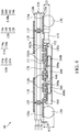
- FIG. 1 is a cross-sectional view of an exemplary semiconductor package structure 10 in accordance with some embodiments.
- the semiconductor package structure 10 is a wafer-level semiconductor package structure, and is a flip-chip semiconductor package structure.
- the semiconductor package structure 10 may be mounted on a base (not shown).
- the semiconductor package structure 10 may be a system-on-chip (SOC) package structure.
- the base may include a printed circuit board (PCB) and may be formed of polypropylene (PP).
- PCB printed circuit board
- PP polypropylene
- the base is a package substrate.
- the semiconductor package structure 10 is mounted onto the base by a bonding process.
- the semiconductor package structure 10 includes electrical connectors 150 that are mounted on and electrically coupled to the base by the bonding process.
- each of the electrical connectors 150 includes a conductive bump structure such as a copper bump or a solder ball, as shown in FIG. 1 .
- each of the electrical connectors 150 includes a conductive pillar structure, a conductive wire structure, or a conductive paste structure.
- the semiconductor package structure 10 further includes a semiconductor package 110a, electrical connectors 140, and an antenna device 130 stacked on and mounted onto the underlying semiconductor package 110a via the electrical connectors 140, as shown in FIG. 1 .
- each of the electrical connectors 140 includes a conductive bump structure such as a copper bump or a solder ball.
- each of the electrical connectors 140 includes a conductive pillar structure, a conductive wire structure, or a conductive paste structure.
- the electrical connectors 140 and the electrical connectors 150 are solder balls, and a ball size of electrical connectors is different than that of the plurality of first electrical connectors. For example, the height H1 of the electrical connectors 140 is lower than the height H2 of the electrical connectors 150, as shown in FIG. 1 .
- the semiconductor package 110a includes a semiconductor die 100.
- the semiconductor die 100 is a system-on-chip (SOC) die that may include a microcontroller (MCU), a microprocessor (MPU), a power management integrated circuit (PMIC), a global positioning system (GPS) device, or a radio frequency (RF) device or any combination thereof.
- SOC system-on-chip
- MCU microcontroller
- MPU microprocessor
- PMIC power management integrated circuit
- GPS global positioning system
- RF radio frequency
- the semiconductor die 100 has two opposing sides. More specifically, the semiconductor die 100 has an active surface 100a and a non-active surface 100b opposite to the active surface 100a.
- the non-active surface 100b may also be referred to as a rear surface and the active surface 100a may also be referred to as a front surface that is opposite to the rear surface.
- the semiconductor die 100 includes pads 101 that are disposed on the active surface 100a and electrically connected to one or more functional circuits (not shown) of the semiconductor die 100.
- the pads 101 of the semiconductor die 100 belong to the uppermost metal layer of the interconnection structure (not shown) of the semiconductor die 100.
- the semiconductor package 110a of the semiconductor package structure 10 includes a redistribution layer (RDL) structure 102 having a first surface 102a and a second surface 102b opposite the first surface 102a.
- the RDL structure 102 which is also referred to as a fan-out RDL structure.
- the RDL structure 102 is disposed on the active surface 100a of the semiconductor die 100 and electrically connected to the semiconductor die 100 through the pads 101 of the semiconductor die 100.
- the RDL structure 102 includes one or more conductive traces disposed in an inter-metal dielectric (IMD) layer.
- first conductive traces are disposed at a first layer-level of the IMD layer adjacent to the first surface 102a of the RDL structure 102. At least one of the first conductive traces is electrically coupled to the semiconductor die 100.
- second conductive traces are disposed at a second layer-level higher than the first layer-level of the IMD layer and adjacent to the second surface 102b of the RDL structure 102.
- at least one of the second conductive traces is bonded and electrically coupled to one or more electrical connectors 140, so that the electrical connectors 140 are electrically coupled to the semiconductor die 100 via the RDL structure 102.
- the IMD layer may include a first sub-dielectric layer and a second sub-dielectric layer successively stacked from the active surface 100a of the semiconductor die 100, such that the first conductive traces are formed in the first sub-dielectric layer and the second conductive traces are formed in the second sub-dielectric layer.
- the IMD layer is formed of an organic material, which includes a polymer base material, a non-organic material, which includes silicon nitride (SiNx), silicon oxide (SiO X ), graphene, or the like.
- the first sub-dielectric layers and the second sub-dielectric layer may be made of a polymer base material.
- the IMD layer is made of a high-k (k is the dielectric constant of the dielectric layer) dielectric layer.
- the number of conductive traces and the number of sub-dielectric layers of the RDL structure 102 shown in FIG. 1 are only an example and are not a limitation to that disclosed in the embodiment.
- the semiconductor package 110a of the semiconductor package structure 10 further includes an encapsulating layer 104 formed on the first surface 102a of the RDL structure 102.
- the encapsulating layer 104 surrounds the semiconductor die 100 and covers the non-active surface 100a of the semiconductor die 100.
- the encapsulating layer 104 has a sidewall (or edge) that is substantially aligned to (or level with) the sidewall (or edge) of the RDL structure 102.
- the encapsulating layer 104 and the semiconductor die 100 are separated from the electrical connectors 140 through the RDL structure 102.
- the electrical connectors 140 are free from contact with the encapsulating layer 104 and the semiconductor die 100.
- the encapsulating layer 104 may be made of a molding compound material, such as an epoxy, a resin, a moldable polymer, or the like.
- the molding compound material may be applied while substantially liquid, and then may be cured through a chemical reaction, such as in an epoxy or resin.
- the molding compound material may be an ultraviolet (UV) or thermally cured polymer applied as a gel or malleable solid capable of being disposed around the semiconductor die 100, and then is cured through a UV or thermal curing process.
- the molding compound material may be cured with a mold (not shown).
- the antenna device 130 includes an insulating substrate 120.
- the insulating substrate 120 has a first surface 120a and a second surface 120b opposite the first surface 120a.
- the first surface 120a of the insulating substrate 120 is adhered to the second surface RDL structure 102 via the electrical connectors 140.
- the insulating substrate 120 may be a single layer or a multi-layer structure and include any one of core insulating materials, for example, glass epoxy resin, bismaleimide-triazine (BT), or ABF.
- the insulating substrate 120 includes a first sub-dielectric layer 115a, a second sub-dielectric layer 115b, and a third sub-dielectric layer 115c successively stacked from the first surface 120a of the insulating substrate 120.
- the antenna device 130 includes a conductive pattern layer 116 including a first antenna element 116a and one or more conductive traces 116b, formed in the first sub-dielectric layer 115a of insulating substrate 120.
- the first antenna element 116a is bonded and electrically connected to one or more electrical connectors 150 and the conductive traces 116b are bonded and electrically connected to electrical connectors 140 and 150.
- the electrical connectors 140 bonded between the RDL structure 102 and the conductive pattern layer 116, so that the conductive pattern layer 116 is separated from the RDL structure 102 by a gap 141.
- the electrical connectors 150 are electrically connected to the first antenna element 116a of the conductive pattern layer 116 and surround the semiconductor package 110a.
- the antenna device 130 further includes a second antenna element 118 formed on the second surface 120b of the insulating substrate 120 (i.e., the top surface of the third sub-dielectric layer 115c) and one or more through-via structures 119 formed in the first sub-dielectric layer 115a, the second sub-dielectric layer 115b, and the third sub-dielectric layer 115c.
- the through-via structures 119 may be referred to as through insulator vias (TIVs) and are electrically connected between the first antenna element 116a and the second antenna element 118, so as to form an antenna in the antenna device 130.
- the conductive pattern layer 116, the second antenna element 118, and the through-via structures 119 are made of a metal material, such as copper or another suitable antenna material.
- the number of conductive pattern layers and the number of sub-dielectric layers of the insulating substrate shown in FIG. 1 are only an example and are not a limitation to that disclosed in the embodiment.
- FIG. 2 is a cross-sectional view of an exemplary semiconductor package structure 20 in accordance with some embodiments of the disclosure. Descriptions of elements of the embodiments hereinafter that are the same as or similar to those previously described with reference to FIG. 1 may be omitted for brevity.
- the semiconductor package structure 20 is similar to the semiconductor package structure 10 shown in FIG. 1 .
- the semiconductor package 110b of the semiconductor package structure 20 includes more than one semiconductor dies.
- the semiconductor package 110b includes semiconductor dies 200 and 300 electrically connected to the RDL structure 102 and surrounded by the encapsulating layer 104. More specifically, similar to the semiconductor die 100 shown in FIG.
- the semiconductor die 200 has an active surface 200a and a non-active surface 200b opposite to the active surface 200a.
- the semiconductor die 300 has an active surface 300a and a non-active surface 300b opposite to the active surface 300a.
- the RDL structure 102 is disposed on and bonded to the active surface 200a of the semiconductor die 200 and the active surface 300a of the semiconductor die 300, so that semiconductor die 100 through the pads 101 of the semiconductor die 100.
- a dimension of the semiconductor die 200 is different than a dimension of the semiconductor die 300.
- the dimension of the semiconductor die 200 is smaller than the dimension of the semiconductor die 300.
- FIG. 2 the number of semiconductor die shown in FIG. 2 is only an example and are not a limitation to that disclosed in the embodiment.
- a functional circuit of the semiconductor die 200 is different than that of the semiconductor die 300.
- the semiconductor die 200 and/or the semiconductor die 300 is a logic die including a central processing unit (CPU), a graphics processing unit (GPU), a dynamic random access memory (DRAM) controller or any combination thereof.
- the semiconductor die 200 and/or the semiconductor die 300 are a system-on-chip (SOC) die. In those cases, the semiconductor dies 200 and 300 can be formed by different technology nodes.
- FIG. 3 is a cross-sectional view of an exemplary semiconductor package structure 30 in accordance with some embodiments of the disclosure. Descriptions of elements of the embodiments hereinafter that are the same as or similar to those previously described with reference to FIG. 2 may be omitted for brevity.
- the semiconductor package structure 30 is similar to the semiconductor package structure 20 shown in FIG. 2 , except that the semiconductor package structure 30 further includes a passive device 170 formed in the gap 141 between the conductive pattern layer 116 and the RDL structure 102 and electrically connected to the RDL structure 102.
- the passive device 170 may be disposed between at least two electrical connectors 114, as shown in FIG. 3 .
- the passive device 170 includes a capacitor, an inductor, a resistor, or a combination thereof. In some embodiments, the passive device 170 is an integrated passive device (IPD). In some embodiments, passive device 170 may contact the second surface 120b of the insulating substrate 120.
- IPD integrated passive device
- FIG. 4 is a cross-sectional view of an exemplary semiconductor package structure 40 in accordance with some embodiments of the disclosure. Descriptions of elements of the embodiments hereinafter that are the same as or similar to those previously described with reference to FIG. 3 may be omitted for brevity.
- the semiconductor package structure 40 is similar to the semiconductor package structure 30 shown in FIG. 3 , except that the semiconductor package structure 40 further includes a passive device 172 that has a different dimension than that of the passive device 170.
- the passive device 172 is electrically connected to the conductive pattern layer 116 and between the semiconductor package 110b and at least one of the electrical connectors 150. In some embodiments, the passive device 172 has a greater dimension than that of the passive device 170.
- the passive device 172 has a dimension (e.g., a height H3) greater than that of the electrical connectors 140 and the passive device 170.
- the passive device 172 has the height H3 that is not less than 100um, and the passive device 170 has a height that is not greater than 100um.
- the height H3 of the passive device 172 is greater than the height of the passive deivce 170.
- a semiconductor package structure comprising: an antenna device, comprising: a conductive pattern layer comprising a first antenna element, formed in an insulating substrate and adjacent to a first surface of the insulating substrate; and a second antenna element formed on a second surface of the insulating substrate opposite the first surface; and a semiconductor package, comprising: a redistribution layer (RDL) structure bonded and electrically connected to the conductive pattern layer; a first semiconductor die electrically connected to the RDL structure; and an encapsulating layer formed on the RDL structure and surrounding the first semiconductor die.
- RDL redistribution layer
- the semiconductor package structure may further comprise: a plurality of first electrical connectors bonding the RDL structure to the conductive pattern layer, so that the conductive pattern layer is separated from the RDL structure by a gap; and a plurality of second electrical connectors electrically connected to the conductive pattern layer and surrounding the semiconductor package.
- the plurality of first electrical connectors and the plurality of second electrical connectors may be solder balls, and a ball size of the plurality of second electrical connectors may be different than a ball size of the plurality of first electrical connectors.
- the semiconductor package structure may further comprise: a passive device formed in the gap between the conductive pattern layer and the RDL structure and electrically connected to the RDL structure.
- the semiconductor package structure alternatively may further comprise: a passive device electrically connected to the conductive pattern layer and between the semiconductor package and at least one of the second electrical connectors.
- the plurality of first electrical connectors may have a height that is lower than a height of the passive device.
- the semiconductor package may further comprise: a second semiconductor die electrically connected to the RDL structure and surrounded by the encapsulating layer, wherein a dimension of the second semiconductor die is different than a dimension of the first semiconductor die.
- the semiconductor package alternatively may further comprise: a second semiconductor die electrically connected to the RDL structure and surrounded by the encapsulating layer, wherein a functional circuit of the second semiconductor die is different than a functional circuit of the first semiconductor die.
- the antenna device may further comprise: at least one through-via structure formed in the insulating substrate and electrically connected between the first antenna element and the second antenna element.
- a semiconductor package structure comprising: a redistribution (RDL) structure having a first surface and a second surface opposite the first surface; a first semiconductor die having an active surface formed on the first surface of the RDL structure; a plurality of first electrical connectors formed on the second surface of the RDL structure; an insulating substrate having a first surface stacked on the second surface of the RDL structure; a conductive pattern layer comprising a first antenna element, formed in the insulating substrate and adjacent to the first surface of the insulating substrate; a second antenna element formed on a second surface of the insulating substrate opposite the first surface of the insulating substrate; and a plurality of second electrical connectors formed on the first surface of the insulating substrate and electrically connected to the first antenna element, wherein a size of the plurality of second electrical connectors is greater than a size of the plurality of first electrical connectors.
- RDL redistribution
- the plurality of first electrical connectors and the plurality of second electrical connectors may be solder balls.
- the semiconductor package structure may further comprise: a passive device formed between two adjacent first electrical connectors of the first electrical connectors and electrically connected to the RDL structure.
- the semiconductor package structure alternatively may further comprise: a passive device electrically connected to the conductive pattern layer and between at least one of the first electrical connectors and at least one of the second electrical connectors.
- the plurality of first electrical connectors may have a height that is lower than the height of the passive device.
- the semiconductor package structure may further comprise: an encapsulating layer formed on the first surface of the RDL structure and surrounding the first semiconductor die.
- the semiconductor package structure may further comprise: a second semiconductor die having an active surface formed on the first surface of the RDL structure; and an encapsulating layer formed on the first surface of the RDL structure and between and surrounding the first semiconductor die and the second semiconductor die.
- a dimension of the second semiconductor die may be different than a dimension of the first semiconductor die.
- a functional circuit of the second semiconductor die also may be different than a functional circuit of the first semiconductor die.
- the semiconductor package structure may further comprise: at least one through-via structure formed in the insulating substrate and electrically connected between the first antenna element and the second antenna element.
- the plurality of first electrical connectors may be electrically connected between the RDL structure and the conductive pattern layer.
- the semiconductor package structure is designed to fabricate an antenna integrated into the semiconductor package structure.
- the antenna is formed in an insulating substrate which is bonded to an RDL structure of the semiconductor package by the use of bump structures (e.g., solder balls).
- bump structures e.g., solder balls.
- the thickness of the insulating substrate with the antenna can be reduced due to the fin pitch RDL structure of the underlying semiconductor package.
- the size of the semiconductor package structure and the die to antenna loss can be reduced.
- Compact to fan-out package integrated with an antenna the manufacturing cost of the semiconductor package structure can be reduced and the process for the fabrication of the semiconductor package structure can be simplified because the antenna is fabricated by a mature substrate technology.
- the thickness of the insulating substrate with the antenna therein is reduced to provide short heat-dissipation path of the semiconductor die in the semiconductor package, thermal performance can be improved.
- the antenna is formed in the insulating substrate that is separated from the semiconductor package having the semiconductor die therein, known good die package and known good antenna can be used during the fabrication of the semiconductor package structure, thereby preventing the yield loss and reducing the manufacturing cost of the semiconductor package structure further.
- the die partition can be enabled and the process for the fabrication of the semiconductor package can be simplified, thereby reducing the manufacturing cost of the semiconductor package.
Landscapes
- Engineering & Computer Science (AREA)
- Microelectronics & Electronic Packaging (AREA)
- Production Of Multi-Layered Print Wiring Board (AREA)
- Physics & Mathematics (AREA)
- Geometry (AREA)
Abstract
Description
- This application claims the benefit of
U.S. Provisional Application No. 62/881,437 filed on August 1, 2019 - The present invention relates to a package structure, and in particular to a fan-out semiconductor package structure that includes antennas.
- In order to ensure the continued miniaturization and multi-functionality of electronic products and communication devices, semiconductor packages must be small in size, support multi-pin connection, operate at high speeds, and have high functionality. Additionally, in a high-frequency application such as a radio frequency (RF) system-in-package (SiP) assembly, antennas are typically used for enabling wireless communication.
- When wireless communication packages with antennas are constructed, package designs need to provide good antenna properties (such as high efficiency, wide bandwidth, etc) while providing reliable and low-cost package solutions. In a conventional semiconductor package structure, a substrate based antenna is bonded with a chip. Since the substrate based antenna is thick, it is difficult to reduce the package size, and high chip to antenna loss is induced due to long trace length. Moreover, substrate based antenna provide a poor thermal performance due to the long heat-dissipation path of the chip bonded thereon.
- Thus, a novel semiconductor package structure is desirable.
- Semiconductor package structures are provided. An exemplary embodiment of a semiconductor package structure includes an antenna device and semiconductor package. The antenna device includes a conductive pattern layer including a first antenna element, formed in an insulating substrate and adjacent to a first surface of the insulating substrate. The antenna device also includes a second antenna element formed on a second surface of the insulating substrate opposite the first surface. The semiconductor package includes a redistribution layer (RDL) structure bonded and electrically connected to the conductive pattern layer. The semiconductor package also includes a first semiconductor die electrically connected to the RDL structure, and an encapsulating layer formed on the RDL structure and surrounding the first semiconductor die.
- Another exemplary embodiment of a semiconductor package structure includes a redistribution (RDL) structure having a first surface and a second surface opposite the first surface, a first semiconductor die having an active surface formed on the first surface of the RDL structure, and a plurality of first electrical connectors formed on the second surface of the RDL structure. The semiconductor package structure also includes an insulating substrate having a first surface stacked on the second surface of the RDL structure. A conductive pattern layer including a first antenna element is formed in the insulating substrate and adjacent to the first surface of the insulating substrate. The semiconductor package structure further includes a second antenna element formed on a second surface of the insulating substrate opposite the first surface of the insulating substrate. In addition, the semiconductor package structure includes a plurality of second electrical connectors formed on the first surface of the insulating substrate and electrically connected to the first antenna element. A size of the plurality of second electrical connectors is greater than a size of the plurality of first electrical connectors.
- A detailed description is given in the following embodiments with reference to the accompanying drawings.
- The present invention can be more fully understood by reading the subsequent detailed description and examples with references made to the accompanying drawings, wherein:
-
FIG. 1 is a cross-sectional view of an exemplary semiconductor package structure in accordance with some embodiments. -
FIG. 2 is a cross-sectional view of an exemplary semiconductor package structure in accordance with some embodiments. -
FIG. 3 is a cross-sectional view of an exemplary semiconductor package structure in accordance with some embodiments. -
FIG. 4 is a cross-sectional view of an exemplary semiconductor package structure in accordance with some embodiments. - The following description is of the best-contemplated mode of carrying out the invention. This description is made for the purpose of illustrating the general principles of the invention and should not be taken in a limiting sense. The scope of the invention is determined by reference to the appended claims.
- The present invention will be described with respect to particular embodiments and with reference to certain drawings, but the invention is not limited thereto and is only limited by the claims. The drawings described are only schematic and are non-limiting. In the drawings, the size of some of the elements may be exaggerated for illustrative purposes and not drawn to scale. The dimensions and the relative dimensions do not correspond to actual dimensions in the practice of the invention.
-
FIG. 1 is a cross-sectional view of an exemplarysemiconductor package structure 10 in accordance with some embodiments. In some embodiments, thesemiconductor package structure 10 is a wafer-level semiconductor package structure, and is a flip-chip semiconductor package structure. Thesemiconductor package structure 10 may be mounted on a base (not shown). For example, thesemiconductor package structure 10 may be a system-on-chip (SOC) package structure. Moreover, the base may include a printed circuit board (PCB) and may be formed of polypropylene (PP). - Alternatively, the base is a package substrate. The
semiconductor package structure 10 is mounted onto the base by a bonding process. For example, thesemiconductor package structure 10 includeselectrical connectors 150 that are mounted on and electrically coupled to the base by the bonding process. In some embodiments, each of theelectrical connectors 150 includes a conductive bump structure such as a copper bump or a solder ball, as shown inFIG. 1 . Alternatively, each of theelectrical connectors 150 includes a conductive pillar structure, a conductive wire structure, or a conductive paste structure. - In some embodiments, the
semiconductor package structure 10 further includes asemiconductor package 110a,electrical connectors 140, and anantenna device 130 stacked on and mounted onto theunderlying semiconductor package 110a via theelectrical connectors 140, as shown inFIG. 1 . In some embodiments, each of theelectrical connectors 140 includes a conductive bump structure such as a copper bump or a solder ball. Alternatively, each of theelectrical connectors 140 includes a conductive pillar structure, a conductive wire structure, or a conductive paste structure. In some embodiments, theelectrical connectors 140 and theelectrical connectors 150 are solder balls, and a ball size of electrical connectors is different than that of the plurality of first electrical connectors. For example, the height H1 of theelectrical connectors 140 is lower than the height H2 of theelectrical connectors 150, as shown inFIG. 1 . - In some embodiments, the
semiconductor package 110a includes asemiconductor die 100. For example, the semiconductor die 100 is a system-on-chip (SOC) die that may include a microcontroller (MCU), a microprocessor (MPU), a power management integrated circuit (PMIC), a global positioning system (GPS) device, or a radio frequency (RF) device or any combination thereof. - The semiconductor die 100 has two opposing sides. More specifically, the
semiconductor die 100 has anactive surface 100a and anon-active surface 100b opposite to theactive surface 100a. Thenon-active surface 100b may also be referred to as a rear surface and theactive surface 100a may also be referred to as a front surface that is opposite to the rear surface. In some embodiments, thesemiconductor die 100 includespads 101 that are disposed on theactive surface 100a and electrically connected to one or more functional circuits (not shown) of thesemiconductor die 100. In some embodiments, thepads 101 of the semiconductor die 100 belong to the uppermost metal layer of the interconnection structure (not shown) of thesemiconductor die 100. - In some embodiments, the
semiconductor package 110a of thesemiconductor package structure 10 includes a redistribution layer (RDL)structure 102 having afirst surface 102a and asecond surface 102b opposite thefirst surface 102a. TheRDL structure 102, which is also referred to as a fan-out RDL structure. In some embodiments, theRDL structure 102 is disposed on theactive surface 100a of thesemiconductor die 100 and electrically connected to the semiconductor die 100 through thepads 101 of the semiconductor die 100. - In some embodiments, the
RDL structure 102 includes one or more conductive traces disposed in an inter-metal dielectric (IMD) layer. For example, first conductive traces are disposed at a first layer-level of the IMD layer adjacent to thefirst surface 102a of theRDL structure 102. At least one of the first conductive traces is electrically coupled to the semiconductor die 100. Moreover, second conductive traces are disposed at a second layer-level higher than the first layer-level of the IMD layer and adjacent to thesecond surface 102b of theRDL structure 102. Moreover, at least one of the second conductive traces is bonded and electrically coupled to one or moreelectrical connectors 140, so that theelectrical connectors 140 are electrically coupled to the semiconductor die 100 via theRDL structure 102. - The IMD layer may include a first sub-dielectric layer and a second sub-dielectric layer successively stacked from the
active surface 100a of the semiconductor die 100, such that the first conductive traces are formed in the first sub-dielectric layer and the second conductive traces are formed in the second sub-dielectric layer. In some embodiments, the IMD layer is formed of an organic material, which includes a polymer base material, a non-organic material, which includes silicon nitride (SiNx), silicon oxide (SiOX), graphene, or the like. For example, the first sub-dielectric layers and the second sub-dielectric layer may be made of a polymer base material. In some other embodiments, the IMD layer is made of a high-k (k is the dielectric constant of the dielectric layer) dielectric layer. - It should be noted that the number of conductive traces and the number of sub-dielectric layers of the
RDL structure 102 shown inFIG. 1 are only an example and are not a limitation to that disclosed in the embodiment. - In some embodiments, the
semiconductor package 110a of thesemiconductor package structure 10 further includes anencapsulating layer 104 formed on thefirst surface 102a of theRDL structure 102. Theencapsulating layer 104 surrounds the semiconductor die 100 and covers thenon-active surface 100a of the semiconductor die 100. Theencapsulating layer 104 has a sidewall (or edge) that is substantially aligned to (or level with) the sidewall (or edge) of theRDL structure 102. - Moreover, the
encapsulating layer 104 and the semiconductor die 100 are separated from theelectrical connectors 140 through theRDL structure 102. In other words, theelectrical connectors 140 are free from contact with theencapsulating layer 104 and the semiconductor die 100. - The
encapsulating layer 104 may be made of a molding compound material, such as an epoxy, a resin, a moldable polymer, or the like. The molding compound material may be applied while substantially liquid, and then may be cured through a chemical reaction, such as in an epoxy or resin. For example, the molding compound material may be an ultraviolet (UV) or thermally cured polymer applied as a gel or malleable solid capable of being disposed around the semiconductor die 100, and then is cured through a UV or thermal curing process. The molding compound material may be cured with a mold (not shown). - In some embodiments, the
antenna device 130 includes an insulatingsubstrate 120. The insulatingsubstrate 120 has afirst surface 120a and asecond surface 120b opposite thefirst surface 120a. In some embodiments, thefirst surface 120a of the insulatingsubstrate 120 is adhered to the secondsurface RDL structure 102 via theelectrical connectors 140. - The insulating
substrate 120 may be a single layer or a multi-layer structure and include any one of core insulating materials, for example, glass epoxy resin, bismaleimide-triazine (BT), or ABF. In some embodiments, the insulatingsubstrate 120 includes a firstsub-dielectric layer 115a, a secondsub-dielectric layer 115b, and a thirdsub-dielectric layer 115c successively stacked from thefirst surface 120a of the insulatingsubstrate 120. - In some embodiments, the
antenna device 130 includes aconductive pattern layer 116 including afirst antenna element 116a and one or moreconductive traces 116b, formed in the firstsub-dielectric layer 115a of insulatingsubstrate 120. Thefirst antenna element 116a is bonded and electrically connected to one or moreelectrical connectors 150 and theconductive traces 116b are bonded and electrically connected toelectrical connectors - In those cases, the
electrical connectors 140 bonded between theRDL structure 102 and theconductive pattern layer 116, so that theconductive pattern layer 116 is separated from theRDL structure 102 by agap 141. Moreover, theelectrical connectors 150 are electrically connected to thefirst antenna element 116a of theconductive pattern layer 116 and surround thesemiconductor package 110a. - In some embodiments, the
antenna device 130 further includes asecond antenna element 118 formed on thesecond surface 120b of the insulating substrate 120 (i.e., the top surface of the thirdsub-dielectric layer 115c) and one or more through-viastructures 119 formed in the firstsub-dielectric layer 115a, the secondsub-dielectric layer 115b, and the thirdsub-dielectric layer 115c. The through-viastructures 119 may be referred to as through insulator vias (TIVs) and are electrically connected between thefirst antenna element 116a and thesecond antenna element 118, so as to form an antenna in theantenna device 130. In some embodiments, theconductive pattern layer 116, thesecond antenna element 118, and the through-viastructures 119 are made of a metal material, such as copper or another suitable antenna material. - It should be noted that the number of conductive pattern layers and the number of sub-dielectric layers of the insulating substrate shown in
FIG. 1 are only an example and are not a limitation to that disclosed in the embodiment. -
FIG. 2 is a cross-sectional view of an exemplarysemiconductor package structure 20 in accordance with some embodiments of the disclosure. Descriptions of elements of the embodiments hereinafter that are the same as or similar to those previously described with reference toFIG. 1 may be omitted for brevity. In the embodiment, thesemiconductor package structure 20 is similar to thesemiconductor package structure 10 shown inFIG. 1 . As shown inFIG. 2 , unlike thesemiconductor package 110a of thesemiconductor package structure 10, thesemiconductor package 110b of thesemiconductor package structure 20 includes more than one semiconductor dies. In some embodiments, thesemiconductor package 110b includes semiconductor dies 200 and 300 electrically connected to theRDL structure 102 and surrounded by theencapsulating layer 104. More specifically, similar to the semiconductor die 100 shown inFIG. 1 , the semiconductor die 200 has anactive surface 200a and anon-active surface 200b opposite to theactive surface 200a. The semiconductor die 300 has anactive surface 300a and anon-active surface 300b opposite to theactive surface 300a. Moreover, theRDL structure 102 is disposed on and bonded to theactive surface 200a of the semiconductor die 200 and theactive surface 300a of the semiconductor die 300, so that semiconductor die 100 through thepads 101 of the semiconductor die 100. - In some embodiments, a dimension of the semiconductor die 200 is different than a dimension of the semiconductor die 300. For example, the dimension of the semiconductor die 200 is smaller than the dimension of the semiconductor die 300.
- It should be noted that the number of semiconductor die shown in
FIG. 2 is only an example and are not a limitation to that disclosed in the embodiment. - In some other embodiments, a functional circuit of the semiconductor die 200 is different than that of the semiconductor die 300. For example, the semiconductor die 200 and/or the semiconductor die 300 is a logic die including a central processing unit (CPU), a graphics processing unit (GPU), a dynamic random access memory (DRAM) controller or any combination thereof. Alternatively, the semiconductor die 200 and/or the semiconductor die 300 are a system-on-chip (SOC) die. In those cases, the semiconductor dies 200 and 300 can be formed by different technology nodes.
-
FIG. 3 is a cross-sectional view of an exemplarysemiconductor package structure 30 in accordance with some embodiments of the disclosure. Descriptions of elements of the embodiments hereinafter that are the same as or similar to those previously described with reference toFIG. 2 may be omitted for brevity. In the embodiment, thesemiconductor package structure 30 is similar to thesemiconductor package structure 20 shown inFIG. 2 , except that thesemiconductor package structure 30 further includes apassive device 170 formed in thegap 141 between theconductive pattern layer 116 and theRDL structure 102 and electrically connected to theRDL structure 102. Thepassive device 170 may be disposed between at least two electrical connectors 114, as shown inFIG. 3 . In some embodiments, thepassive device 170 includes a capacitor, an inductor, a resistor, or a combination thereof. In some embodiments, thepassive device 170 is an integrated passive device (IPD). In some embodiments,passive device 170 may contact thesecond surface 120b of the insulatingsubstrate 120. -
FIG. 4 is a cross-sectional view of an exemplarysemiconductor package structure 40 in accordance with some embodiments of the disclosure. Descriptions of elements of the embodiments hereinafter that are the same as or similar to those previously described with reference toFIG. 3 may be omitted for brevity. In the embodiment, thesemiconductor package structure 40 is similar to thesemiconductor package structure 30 shown inFIG. 3 , except that thesemiconductor package structure 40 further includes apassive device 172 that has a different dimension than that of thepassive device 170. In some embodiments, thepassive device 172 is electrically connected to theconductive pattern layer 116 and between thesemiconductor package 110b and at least one of theelectrical connectors 150. In some embodiments, thepassive device 172 has a greater dimension than that of thepassive device 170. Moreover, thepassive device 172 has a dimension (e.g., a height H3) greater than that of theelectrical connectors 140 and thepassive device 170. As an example, thepassive device 172 has the height H3 that is not less than 100um, and thepassive device 170 has a height that is not greater than 100um. Moreover, the height H3 of thepassive device 172 is greater than the height of thepassive deivce 170. - According to one aspect, a semiconductor package structure is provided, comprising: an antenna device, comprising: a conductive pattern layer comprising a first antenna element, formed in an insulating substrate and adjacent to a first surface of the insulating substrate; and a second antenna element formed on a second surface of the insulating substrate opposite the first surface; and a semiconductor package, comprising: a redistribution layer (RDL) structure bonded and electrically connected to the conductive pattern layer; a first semiconductor die electrically connected to the RDL structure; and an encapsulating layer formed on the RDL structure and surrounding the first semiconductor die.
- The semiconductor package structure may further comprise: a plurality of first electrical connectors bonding the RDL structure to the conductive pattern layer, so that the conductive pattern layer is separated from the RDL structure by a gap; and a plurality of second electrical connectors electrically connected to the conductive pattern layer and surrounding the semiconductor package.
- The plurality of first electrical connectors and the plurality of second electrical connectors may be solder balls, and a ball size of the plurality of second electrical connectors may be different than a ball size of the plurality of first electrical connectors.
- The semiconductor package structure may further comprise: a passive device formed in the gap between the conductive pattern layer and the RDL structure and electrically connected to the RDL structure.
- The semiconductor package structure alternatively may further comprise: a passive device electrically connected to the conductive pattern layer and between the semiconductor package and at least one of the second electrical connectors.
- The plurality of first electrical connectors may have a height that is lower than a height of the passive device.
- The semiconductor package may further comprise: a second semiconductor die electrically connected to the RDL structure and surrounded by the encapsulating layer, wherein a dimension of the second semiconductor die is different than a dimension of the first semiconductor die.
- The semiconductor package alternatively may further comprise: a second semiconductor die electrically connected to the RDL structure and surrounded by the encapsulating layer, wherein a functional circuit of the second semiconductor die is different than a functional circuit of the first semiconductor die.
- The antenna device may further comprise: at least one through-via structure formed in the insulating substrate and electrically connected between the first antenna element and the second antenna element.
- According to a further aspect, a semiconductor package structure is provided, comprising: a redistribution (RDL) structure having a first surface and a second surface opposite the first surface; a first semiconductor die having an active surface formed on the first surface of the RDL structure; a plurality of first electrical connectors formed on the second surface of the RDL structure; an insulating substrate having a first surface stacked on the second surface of the RDL structure; a conductive pattern layer comprising a first antenna element, formed in the insulating substrate and adjacent to the first surface of the insulating substrate; a second antenna element formed on a second surface of the insulating substrate opposite the first surface of the insulating substrate; and a plurality of second electrical connectors formed on the first surface of the insulating substrate and electrically connected to the first antenna element, wherein a size of the plurality of second electrical connectors is greater than a size of the plurality of first electrical connectors.
- The plurality of first electrical connectors and the plurality of second electrical connectors may be solder balls.
- The semiconductor package structure may further comprise: a passive device formed between two adjacent first electrical connectors of the first electrical connectors and electrically connected to the RDL structure.
- The semiconductor package structure alternatively may further comprise: a passive device electrically connected to the conductive pattern layer and between at least one of the first electrical connectors and at least one of the second electrical connectors.
- The plurality of first electrical connectors may have a height that is lower than the height of the passive device.
- The semiconductor package structure may further comprise: an encapsulating layer formed on the first surface of the RDL structure and surrounding the first semiconductor die.
- The semiconductor package structure may further comprise: a second semiconductor die having an active surface formed on the first surface of the RDL structure; and an encapsulating layer formed on the first surface of the RDL structure and between and surrounding the first semiconductor die and the second semiconductor die.
- A dimension of the second semiconductor die may be different than a dimension of the first semiconductor die.
- A functional circuit of the second semiconductor die also may be different than a functional circuit of the first semiconductor die.
- The semiconductor package structure may further comprise: at least one through-via structure formed in the insulating substrate and electrically connected between the first antenna element and the second antenna element.
- The plurality of first electrical connectors may be electrically connected between the RDL structure and the conductive pattern layer.
- According to the foregoing embodiments, the semiconductor package structure is designed to fabricate an antenna integrated into the semiconductor package structure. In the semiconductor package structure, it allows that the antenna is formed in an insulating substrate which is bonded to an RDL structure of the semiconductor package by the use of bump structures (e.g., solder balls). Compare to a substrate based antenna bonded with a semiconductor die/chip, the thickness of the insulating substrate with the antenna can be reduced due to the fin pitch RDL structure of the underlying semiconductor package. As a result, the size of the semiconductor package structure and the die to antenna loss can be reduced. Compact to fan-out package integrated with an antenna, the manufacturing cost of the semiconductor package structure can be reduced and the process for the fabrication of the semiconductor package structure can be simplified because the antenna is fabricated by a mature substrate technology.
- According to the foregoing embodiments, since the thickness of the insulating substrate with the antenna therein is reduced to provide short heat-dissipation path of the semiconductor die in the semiconductor package, thermal performance can be improved.
- According to the foregoing embodiments, since the antenna is formed in the insulating substrate that is separated from the semiconductor package having the semiconductor die therein, known good die package and known good antenna can be used during the fabrication of the semiconductor package structure, thereby preventing the yield loss and reducing the manufacturing cost of the semiconductor package structure further.
- According to the foregoing embodiments, since the semiconductor dies can be formed by different technology nodes before placing those semiconductor dies in the semiconductor package, the die partition can be enabled and the process for the fabrication of the semiconductor package can be simplified, thereby reducing the manufacturing cost of the semiconductor package.
- According to the foregoing embodiments, since a passive device is integrated in the semiconductor package structure, the electrical performance can be improved.
- According to the foregoing embodiments, since passive devices with different dimensions can be integrated in semiconductor package structures, the electrical performance can be improved further. Moreover, the flexibility of integrating a large passive device into a semiconductor package structure can be increased.
- While the invention has been described by way of example and in terms of the preferred embodiments, it should be understood that the invention is not limited to the disclosed embodiments. On the contrary, it is intended to cover various modifications and similar arrangements (as would be apparent to those skilled in the art). Therefore, the scope of the appended claims should be accorded the broadest interpretation so as to encompass all such modifications and similar arrangements.
Claims (15)
- A semiconductor package structure, comprising:an antenna device, comprising:a conductive pattern layer comprising a first antenna element, formed in an insulating substrate and adjacent to a first surface of the insulating substrate; anda second antenna element formed on a second surface of the insulating substrate opposite the first surface; anda semiconductor package, comprising:a redistribution layer (RDL) structure bonded and electrically connected to the conductive pattern layer;a first semiconductor die electrically connected to the RDL structure.
- The semiconductor package structure as claimed in claim 1, further comprising:a plurality of first electrical connectors bonding the RDL structure to the conductive pattern layer, so that the conductive pattern layer is separated from the RDL structure by a gap; anda plurality of second electrical connectors electrically connected to the conductive pattern layer and surrounding the semiconductor package.
- The semiconductor package structure as claimed in claim 2, wherein the plurality of first electrical connectors and the plurality of second electrical connectors are solder balls, and a ball size of the plurality of second electrical connectors is different than a ball size of the plurality of first electrical connectors.
- The semiconductor package structure as claimed in claim 2 or 3, further comprising:a passive device formed in the gap between the conductive pattern layer and the RDL structure and electrically connected to the RDL structure; ora passive device electrically connected to the conductive pattern layer and between the semiconductor package and at least one of the second electrical connectors.
- The semiconductor package structure as claimed in one of the preceding claims, wherein the semiconductor package further comprises:
an encapsulating layer formed on the RDL structure and surrounding the first semiconductor die. - The semiconductor package structure as claimed in claim 5, further
comprising:a second semiconductor die electrically connected to the RDL structure and surrounded by the encapsulating layer, wherein a dimension of the second semiconductor die is different than a dimension of the first semiconductor die; ora second semiconductor die electrically connected to the RDL structure and surrounded by the encapsulating layer, wherein a functional circuit of the second semiconductor die is different than a functional circuit of the first semiconductor die. - The semiconductor package structure of claim 1, wherein:the redistribution (RDL) structure has a first surface and a second surface opposite the first surface;the first semiconductor die has an active surface formed on the first surface of the RDL structure;a plurality of first electrical connectors are formed on the second surface of the RDL structure;the insulating substrate has its first surface stacked on the second surface of the RDL structure;the conductive pattern layer is formed in the insulating substrate and adjacent to the first surface of the insulating substrate; anda plurality of second electrical connectors are formed on the first surface of the insulating substrate and electrically connected to the first antenna element, wherein a size of the plurality of second electrical connectors is greater than a size of the plurality of first electrical connectors.
- The semiconductor package structure as claimed in claim 7, wherein the plurality of first electrical connectors and the plurality of second electrical connectors are solder balls.
- The semiconductor package structure as claimed in claim 7 or 8, further comprising:a passive device formed between two adjacent first electrical connectors of the first electrical connectors and electrically connected to the RDL structure; ora passive device electrically connected to the conductive pattern layer and between at least one of the first electrical connectors and at least one of the second electrical connectors.
- The semiconductor package structure as claimed in claim 4 or 9, wherein the plurality of first electrical connectors has a height that is lower than the height of the passive device.
- The semiconductor package structure as claimed in one of claims 7 to 10, further comprising:
an encapsulating layer formed on the first surface of the RDL structure and surrounding the first semiconductor die. - The semiconductor package structure as claimed in one of claims 7 to 10, further comprising:a second semiconductor die having an active surface formed on the first surface of the RDL structure; andan encapsulating layer formed on the first surface of the RDL structure and between and surrounding the first semiconductor die and the second semiconductor die.
- The semiconductor package structure as claimed in claim 12, wherein a dimension of the second semiconductor die is different than a dimension of the first semiconductor die; and/or.
a functional circuit of the second semiconductor die is different than a functional circuit of the first semiconductor die. - The semiconductor package structure as claimed in one of claims 7 to 13, wherein the plurality of first electrical connectors is electrically connected between the RDL structure and the conductive pattern layer.
- The semiconductor package structure as claimed in one of the preceding claims, further comprising:
at least one through-via structure formed in the insulating substrate and electrically connected between the first antenna element and the second antenna element.
Applications Claiming Priority (2)
| Application Number | Priority Date | Filing Date | Title |
|---|---|---|---|
| US201962881437P | 2019-08-01 | 2019-08-01 | |
| US16/910,354 US11508678B2 (en) | 2019-08-01 | 2020-06-24 | Semiconductor package structure including antenna |
Publications (2)
| Publication Number | Publication Date |
|---|---|
| EP3772100A1 true EP3772100A1 (en) | 2021-02-03 |
| EP3772100B1 EP3772100B1 (en) | 2024-04-10 |
Family
ID=71614685
Family Applications (1)
| Application Number | Title | Priority Date | Filing Date |
|---|---|---|---|
| EP20185395.9A Active EP3772100B1 (en) | 2019-08-01 | 2020-07-13 | Semiconductor package structure including antenna |
Country Status (4)
| Country | Link |
|---|---|
| US (2) | US11508678B2 (en) |
| EP (1) | EP3772100B1 (en) |
| CN (1) | CN112310061B (en) |
| TW (1) | TWI738445B (en) |
Families Citing this family (8)
| Publication number | Priority date | Publication date | Assignee | Title |
|---|---|---|---|---|
| US11508678B2 (en) * | 2019-08-01 | 2022-11-22 | Mediatek Inc. | Semiconductor package structure including antenna |
| US11600932B2 (en) * | 2020-04-17 | 2023-03-07 | Texas Instruments Incorporated | Antenna-on-package including multiple types of antenna |
| KR102872412B1 (en) * | 2020-04-28 | 2025-10-17 | 삼성디스플레이 주식회사 | Fingerprint sensor and display device including the same |
| US12322856B2 (en) | 2020-12-30 | 2025-06-03 | Texas Instruments Incorporated | Antenna in package having antenna on package substrate |
| US11735830B2 (en) * | 2021-08-06 | 2023-08-22 | Advanced Semiconductor Engineering, Inc. | Antenna device and method for manufacturing the same |
| TWI790054B (en) * | 2021-12-17 | 2023-01-11 | 財團法人工業技術研究院 | Integrated antenna package structure |
| CN121282617A (en) * | 2024-07-03 | 2026-01-06 | 盛合晶微半导体(江阴)有限公司 | Antenna packaging structure and manufacturing method thereof |
| TWI912952B (en) * | 2024-09-27 | 2026-01-21 | 大陸商禮鼎半導體科技秦皇島有限公司 | Packaging substrate and manufacturing method of the same |
Citations (2)
| Publication number | Priority date | Publication date | Assignee | Title |
|---|---|---|---|---|
| US20170365587A1 (en) * | 2016-06-17 | 2017-12-21 | Taiwan Semiconductor Manufacturing Company Ltd. | Semiconductor package and manufacturing method of the same |
| US20190115310A1 (en) * | 2017-05-19 | 2019-04-18 | Samsung Electro-Mechanics Co., Ltd. | Composite antenna substrate and semiconductor package module |
Family Cites Families (15)
| Publication number | Priority date | Publication date | Assignee | Title |
|---|---|---|---|---|
| US9461355B2 (en) | 2013-03-29 | 2016-10-04 | Intel Corporation | Method apparatus and material for radio frequency passives and antennas |
| US20170040266A1 (en) * | 2015-05-05 | 2017-02-09 | Mediatek Inc. | Fan-out package structure including antenna |
| US11335651B2 (en) | 2015-12-22 | 2022-05-17 | Intel Corporation | Microelectronic devices designed with compound semiconductor devices and integrated on an inter die fabric |
| US10483211B2 (en) | 2016-02-22 | 2019-11-19 | Mediatek Inc. | Fan-out package structure and method for forming the same |
| DE112016006695B4 (en) | 2016-04-01 | 2026-01-29 | Intel Corporation | Housing on antenna housing and method for its manufacture |
| CN107393880A (en) | 2016-04-12 | 2017-11-24 | 联发科技股份有限公司 | Semiconductor packaging structure |
| KR102005349B1 (en) * | 2016-06-23 | 2019-07-31 | 삼성전자주식회사 | Fan-out semiconductor package module |
| US9935065B1 (en) | 2016-12-21 | 2018-04-03 | Infineon Technologies Ag | Radio frequency device packages and methods of formation thereof |
| TWI659518B (en) | 2017-05-18 | 2019-05-11 | Siliconware Precision Industries Co., Ltd. | Electronic package and its manufacturing method |
| KR102179166B1 (en) | 2017-05-19 | 2020-11-16 | 삼성전자주식회사 | Antenna substrate and semiconductor combined module |
| US10490880B2 (en) * | 2017-05-26 | 2019-11-26 | Qualcomm Incorporation | Glass-based antenna array package |
| US10847869B2 (en) | 2017-06-07 | 2020-11-24 | Mediatek Inc. | Semiconductor package having discrete antenna device |
| KR101942737B1 (en) * | 2017-08-04 | 2019-01-29 | 삼성전기 주식회사 | Connection system of semiconductor packages |
| TWI640066B (en) * | 2017-11-03 | 2018-11-01 | 矽品精密工業股份有限公司 | Electronic package and its manufacturing method |
| US11508678B2 (en) * | 2019-08-01 | 2022-11-22 | Mediatek Inc. | Semiconductor package structure including antenna |
-
2020
- 2020-06-24 US US16/910,354 patent/US11508678B2/en active Active
- 2020-07-13 EP EP20185395.9A patent/EP3772100B1/en active Active
- 2020-07-31 TW TW109126066A patent/TWI738445B/en active
- 2020-08-03 CN CN202010768717.6A patent/CN112310061B/en active Active
-
2022
- 2022-10-13 US US18/046,218 patent/US11824020B2/en active Active
Patent Citations (2)
| Publication number | Priority date | Publication date | Assignee | Title |
|---|---|---|---|---|
| US20170365587A1 (en) * | 2016-06-17 | 2017-12-21 | Taiwan Semiconductor Manufacturing Company Ltd. | Semiconductor package and manufacturing method of the same |
| US20190115310A1 (en) * | 2017-05-19 | 2019-04-18 | Samsung Electro-Mechanics Co., Ltd. | Composite antenna substrate and semiconductor package module |
Also Published As
| Publication number | Publication date |
|---|---|
| TWI738445B (en) | 2021-09-01 |
| US11508678B2 (en) | 2022-11-22 |
| CN112310061A (en) | 2021-02-02 |
| CN112310061B (en) | 2025-07-11 |
| US20210035930A1 (en) | 2021-02-04 |
| US20230056550A1 (en) | 2023-02-23 |
| EP3772100B1 (en) | 2024-04-10 |
| US11824020B2 (en) | 2023-11-21 |
| TW202107646A (en) | 2021-02-16 |
Similar Documents
| Publication | Publication Date | Title |
|---|---|---|
| EP3772100B1 (en) | Semiconductor package structure including antenna | |
| US11742564B2 (en) | Fan-out package structure with integrated antenna | |
| US11574881B2 (en) | Semiconductor package structure with antenna | |
| US11652273B2 (en) | Innovative air gap for antenna fan out package | |
| US11728292B2 (en) | Semiconductor package assembly having a conductive electromagnetic shield layer | |
| US20190252351A1 (en) | Semiconductor package structure having an antenna pattern electrically coupled to a first redistribution layer (rdl) | |
| US10692789B2 (en) | Stacked fan-out package structure | |
| EP3951870A1 (en) | Method for forming a fan-out package structure | |
| US11830851B2 (en) | Semiconductor package structure | |
| US10199318B2 (en) | Semiconductor package assembly | |
| US10515887B2 (en) | Fan-out package structure having stacked carrier substrates and method for forming the same | |
| EP3273475B1 (en) | Fan-out package structure | |
| US12021031B2 (en) | Semiconductor package structure | |
| US11670596B2 (en) | Semiconductor package structure | |
| US10147674B2 (en) | Semiconductor package assembly |
Legal Events
| Date | Code | Title | Description |
|---|---|---|---|
| PUAI | Public reference made under article 153(3) epc to a published international application that has entered the european phase |
Free format text: ORIGINAL CODE: 0009012 |
|
| STAA | Information on the status of an ep patent application or granted ep patent |
Free format text: STATUS: THE APPLICATION HAS BEEN PUBLISHED |
|
| AK | Designated contracting states |
Kind code of ref document: A1 Designated state(s): AL AT BE BG CH CY CZ DE DK EE ES FI FR GB GR HR HU IE IS IT LI LT LU LV MC MK MT NL NO PL PT RO RS SE SI SK SM TR |
|
| AX | Request for extension of the european patent |
Extension state: BA ME |
|
| RIN1 | Information on inventor provided before grant (corrected) |
Inventor name: CHI, YEN-YAO Inventor name: LIU, NAI-WEI Inventor name: LIN, TZU-HUNG |
|
| RIN1 | Information on inventor provided before grant (corrected) |
Inventor name: LIU, NAI-WEI Inventor name: CHI, YEN-YAO Inventor name: LIN, TZU-HUNG |
|
| STAA | Information on the status of an ep patent application or granted ep patent |
Free format text: STATUS: REQUEST FOR EXAMINATION WAS MADE |
|
| 17P | Request for examination filed |
Effective date: 20210726 |
|
| RBV | Designated contracting states (corrected) |
Designated state(s): AL AT BE BG CH CY CZ DE DK EE ES FI FR GB GR HR HU IE IS IT LI LT LU LV MC MK MT NL NO PL PT RO RS SE SI SK SM TR |
|
| STAA | Information on the status of an ep patent application or granted ep patent |
Free format text: STATUS: EXAMINATION IS IN PROGRESS |
|
| 17Q | First examination report despatched |
Effective date: 20220916 |
|
| P01 | Opt-out of the competence of the unified patent court (upc) registered |
Effective date: 20230607 |
|
| GRAP | Despatch of communication of intention to grant a patent |
Free format text: ORIGINAL CODE: EPIDOSNIGR1 |
|
| STAA | Information on the status of an ep patent application or granted ep patent |
Free format text: STATUS: GRANT OF PATENT IS INTENDED |
|
| RIC1 | Information provided on ipc code assigned before grant |
Ipc: H01L 25/10 20060101ALN20231025BHEP Ipc: H01L 25/065 20060101ALN20231025BHEP Ipc: H05K 1/18 20060101ALI20231025BHEP Ipc: H05K 1/16 20060101ALI20231025BHEP Ipc: H01Q 1/22 20060101ALI20231025BHEP Ipc: H01L 23/538 20060101ALI20231025BHEP Ipc: H01L 23/00 20060101ALI20231025BHEP Ipc: H01L 23/498 20060101ALI20231025BHEP Ipc: H01L 23/31 20060101ALI20231025BHEP Ipc: H01L 23/66 20060101AFI20231025BHEP |
|
| INTG | Intention to grant announced |
Effective date: 20231109 |
|
| RIC1 | Information provided on ipc code assigned before grant |
Ipc: H01L 25/10 20060101ALN20231027BHEP Ipc: H01L 25/065 20060101ALN20231027BHEP Ipc: H05K 1/18 20060101ALI20231027BHEP Ipc: H05K 1/16 20060101ALI20231027BHEP Ipc: H01Q 1/22 20060101ALI20231027BHEP Ipc: H01L 23/538 20060101ALI20231027BHEP Ipc: H01L 23/00 20060101ALI20231027BHEP Ipc: H01L 23/498 20060101ALI20231027BHEP Ipc: H01L 23/31 20060101ALI20231027BHEP Ipc: H01L 23/66 20060101AFI20231027BHEP |
|
| GRAS | Grant fee paid |
Free format text: ORIGINAL CODE: EPIDOSNIGR3 |
|
| GRAA | (expected) grant |
Free format text: ORIGINAL CODE: 0009210 |
|
| STAA | Information on the status of an ep patent application or granted ep patent |
Free format text: STATUS: THE PATENT HAS BEEN GRANTED |
|
| AK | Designated contracting states |
Kind code of ref document: B1 Designated state(s): AL AT BE BG CH CY CZ DE DK EE ES FI FR GB GR HR HU IE IS IT LI LT LU LV MC MK MT NL NO PL PT RO RS SE SI SK SM TR |
|
| REG | Reference to a national code |
Ref country code: GB Ref legal event code: FG4D |
|
| REG | Reference to a national code |
Ref country code: CH Ref legal event code: EP |
|
| REG | Reference to a national code |
Ref country code: DE Ref legal event code: R096 Ref document number: 602020028623 Country of ref document: DE |
|
| REG | Reference to a national code |
Ref country code: IE Ref legal event code: FG4D |
|
| REG | Reference to a national code |
Ref country code: LT Ref legal event code: MG9D |
|
| REG | Reference to a national code |
Ref country code: NL Ref legal event code: MP Effective date: 20240410 |
|
| REG | Reference to a national code |
Ref country code: AT Ref legal event code: MK05 Ref document number: 1675826 Country of ref document: AT Kind code of ref document: T Effective date: 20240410 |
|
| PG25 | Lapsed in a contracting state [announced via postgrant information from national office to epo] |
Ref country code: NL Free format text: LAPSE BECAUSE OF FAILURE TO SUBMIT A TRANSLATION OF THE DESCRIPTION OR TO PAY THE FEE WITHIN THE PRESCRIBED TIME-LIMIT Effective date: 20240410 |
|
| PG25 | Lapsed in a contracting state [announced via postgrant information from national office to epo] |
Ref country code: NL Free format text: LAPSE BECAUSE OF FAILURE TO SUBMIT A TRANSLATION OF THE DESCRIPTION OR TO PAY THE FEE WITHIN THE PRESCRIBED TIME-LIMIT Effective date: 20240410 |
|
| PG25 | Lapsed in a contracting state [announced via postgrant information from national office to epo] |
Ref country code: IS Free format text: LAPSE BECAUSE OF FAILURE TO SUBMIT A TRANSLATION OF THE DESCRIPTION OR TO PAY THE FEE WITHIN THE PRESCRIBED TIME-LIMIT Effective date: 20240810 |
|
| PG25 | Lapsed in a contracting state [announced via postgrant information from national office to epo] |
Ref country code: BG Free format text: LAPSE BECAUSE OF FAILURE TO SUBMIT A TRANSLATION OF THE DESCRIPTION OR TO PAY THE FEE WITHIN THE PRESCRIBED TIME-LIMIT Effective date: 20240410 |
|
| PG25 | Lapsed in a contracting state [announced via postgrant information from national office to epo] |
Ref country code: HR Free format text: LAPSE BECAUSE OF FAILURE TO SUBMIT A TRANSLATION OF THE DESCRIPTION OR TO PAY THE FEE WITHIN THE PRESCRIBED TIME-LIMIT Effective date: 20240410 Ref country code: FI Free format text: LAPSE BECAUSE OF FAILURE TO SUBMIT A TRANSLATION OF THE DESCRIPTION OR TO PAY THE FEE WITHIN THE PRESCRIBED TIME-LIMIT Effective date: 20240410 |
|
| PG25 | Lapsed in a contracting state [announced via postgrant information from national office to epo] |
Ref country code: GR Free format text: LAPSE BECAUSE OF FAILURE TO SUBMIT A TRANSLATION OF THE DESCRIPTION OR TO PAY THE FEE WITHIN THE PRESCRIBED TIME-LIMIT Effective date: 20240711 |
|
| PG25 | Lapsed in a contracting state [announced via postgrant information from national office to epo] |
Ref country code: PT Free format text: LAPSE BECAUSE OF FAILURE TO SUBMIT A TRANSLATION OF THE DESCRIPTION OR TO PAY THE FEE WITHIN THE PRESCRIBED TIME-LIMIT Effective date: 20240812 |
|
| PG25 | Lapsed in a contracting state [announced via postgrant information from national office to epo] |
Ref country code: ES Free format text: LAPSE BECAUSE OF FAILURE TO SUBMIT A TRANSLATION OF THE DESCRIPTION OR TO PAY THE FEE WITHIN THE PRESCRIBED TIME-LIMIT Effective date: 20240410 |
|
| PG25 | Lapsed in a contracting state [announced via postgrant information from national office to epo] |
Ref country code: AT Free format text: LAPSE BECAUSE OF FAILURE TO SUBMIT A TRANSLATION OF THE DESCRIPTION OR TO PAY THE FEE WITHIN THE PRESCRIBED TIME-LIMIT Effective date: 20240410 |
|
| PG25 | Lapsed in a contracting state [announced via postgrant information from national office to epo] |
Ref country code: PL Free format text: LAPSE BECAUSE OF FAILURE TO SUBMIT A TRANSLATION OF THE DESCRIPTION OR TO PAY THE FEE WITHIN THE PRESCRIBED TIME-LIMIT Effective date: 20240410 |
|
| PG25 | Lapsed in a contracting state [announced via postgrant information from national office to epo] |
Ref country code: LV Free format text: LAPSE BECAUSE OF FAILURE TO SUBMIT A TRANSLATION OF THE DESCRIPTION OR TO PAY THE FEE WITHIN THE PRESCRIBED TIME-LIMIT Effective date: 20240410 |
|
| PG25 | Lapsed in a contracting state [announced via postgrant information from national office to epo] |
Ref country code: PT Free format text: LAPSE BECAUSE OF FAILURE TO SUBMIT A TRANSLATION OF THE DESCRIPTION OR TO PAY THE FEE WITHIN THE PRESCRIBED TIME-LIMIT Effective date: 20240812 Ref country code: PL Free format text: LAPSE BECAUSE OF FAILURE TO SUBMIT A TRANSLATION OF THE DESCRIPTION OR TO PAY THE FEE WITHIN THE PRESCRIBED TIME-LIMIT Effective date: 20240410 Ref country code: NO Free format text: LAPSE BECAUSE OF FAILURE TO SUBMIT A TRANSLATION OF THE DESCRIPTION OR TO PAY THE FEE WITHIN THE PRESCRIBED TIME-LIMIT Effective date: 20240710 Ref country code: LV Free format text: LAPSE BECAUSE OF FAILURE TO SUBMIT A TRANSLATION OF THE DESCRIPTION OR TO PAY THE FEE WITHIN THE PRESCRIBED TIME-LIMIT Effective date: 20240410 Ref country code: IS Free format text: LAPSE BECAUSE OF FAILURE TO SUBMIT A TRANSLATION OF THE DESCRIPTION OR TO PAY THE FEE WITHIN THE PRESCRIBED TIME-LIMIT Effective date: 20240810 Ref country code: HR Free format text: LAPSE BECAUSE OF FAILURE TO SUBMIT A TRANSLATION OF THE DESCRIPTION OR TO PAY THE FEE WITHIN THE PRESCRIBED TIME-LIMIT Effective date: 20240410 Ref country code: GR Free format text: LAPSE BECAUSE OF FAILURE TO SUBMIT A TRANSLATION OF THE DESCRIPTION OR TO PAY THE FEE WITHIN THE PRESCRIBED TIME-LIMIT Effective date: 20240711 Ref country code: FI Free format text: LAPSE BECAUSE OF FAILURE TO SUBMIT A TRANSLATION OF THE DESCRIPTION OR TO PAY THE FEE WITHIN THE PRESCRIBED TIME-LIMIT Effective date: 20240410 Ref country code: ES Free format text: LAPSE BECAUSE OF FAILURE TO SUBMIT A TRANSLATION OF THE DESCRIPTION OR TO PAY THE FEE WITHIN THE PRESCRIBED TIME-LIMIT Effective date: 20240410 Ref country code: BG Free format text: LAPSE BECAUSE OF FAILURE TO SUBMIT A TRANSLATION OF THE DESCRIPTION OR TO PAY THE FEE WITHIN THE PRESCRIBED TIME-LIMIT Effective date: 20240410 Ref country code: AT Free format text: LAPSE BECAUSE OF FAILURE TO SUBMIT A TRANSLATION OF THE DESCRIPTION OR TO PAY THE FEE WITHIN THE PRESCRIBED TIME-LIMIT Effective date: 20240410 Ref country code: RS Free format text: LAPSE BECAUSE OF FAILURE TO SUBMIT A TRANSLATION OF THE DESCRIPTION OR TO PAY THE FEE WITHIN THE PRESCRIBED TIME-LIMIT Effective date: 20240710 |
|
| REG | Reference to a national code |
Ref country code: DE Ref legal event code: R097 Ref document number: 602020028623 Country of ref document: DE |
|
| PG25 | Lapsed in a contracting state [announced via postgrant information from national office to epo] |
Ref country code: DK Free format text: LAPSE BECAUSE OF FAILURE TO SUBMIT A TRANSLATION OF THE DESCRIPTION OR TO PAY THE FEE WITHIN THE PRESCRIBED TIME-LIMIT Effective date: 20240410 |
|
| PG25 | Lapsed in a contracting state [announced via postgrant information from national office to epo] |
Ref country code: EE Free format text: LAPSE BECAUSE OF FAILURE TO SUBMIT A TRANSLATION OF THE DESCRIPTION OR TO PAY THE FEE WITHIN THE PRESCRIBED TIME-LIMIT Effective date: 20240410 |
|
| PG25 | Lapsed in a contracting state [announced via postgrant information from national office to epo] |
Ref country code: CZ Free format text: LAPSE BECAUSE OF FAILURE TO SUBMIT A TRANSLATION OF THE DESCRIPTION OR TO PAY THE FEE WITHIN THE PRESCRIBED TIME-LIMIT Effective date: 20240410 |
|
| PG25 | Lapsed in a contracting state [announced via postgrant information from national office to epo] |
Ref country code: SK Free format text: LAPSE BECAUSE OF FAILURE TO SUBMIT A TRANSLATION OF THE DESCRIPTION OR TO PAY THE FEE WITHIN THE PRESCRIBED TIME-LIMIT Effective date: 20240410 Ref country code: RO Free format text: LAPSE BECAUSE OF FAILURE TO SUBMIT A TRANSLATION OF THE DESCRIPTION OR TO PAY THE FEE WITHIN THE PRESCRIBED TIME-LIMIT Effective date: 20240410 |
|
| PG25 | Lapsed in a contracting state [announced via postgrant information from national office to epo] |
Ref country code: SM Free format text: LAPSE BECAUSE OF FAILURE TO SUBMIT A TRANSLATION OF THE DESCRIPTION OR TO PAY THE FEE WITHIN THE PRESCRIBED TIME-LIMIT Effective date: 20240410 |
|
| PG25 | Lapsed in a contracting state [announced via postgrant information from national office to epo] |
Ref country code: SM Free format text: LAPSE BECAUSE OF FAILURE TO SUBMIT A TRANSLATION OF THE DESCRIPTION OR TO PAY THE FEE WITHIN THE PRESCRIBED TIME-LIMIT Effective date: 20240410 Ref country code: SK Free format text: LAPSE BECAUSE OF FAILURE TO SUBMIT A TRANSLATION OF THE DESCRIPTION OR TO PAY THE FEE WITHIN THE PRESCRIBED TIME-LIMIT Effective date: 20240410 Ref country code: RO Free format text: LAPSE BECAUSE OF FAILURE TO SUBMIT A TRANSLATION OF THE DESCRIPTION OR TO PAY THE FEE WITHIN THE PRESCRIBED TIME-LIMIT Effective date: 20240410 Ref country code: EE Free format text: LAPSE BECAUSE OF FAILURE TO SUBMIT A TRANSLATION OF THE DESCRIPTION OR TO PAY THE FEE WITHIN THE PRESCRIBED TIME-LIMIT Effective date: 20240410 Ref country code: DK Free format text: LAPSE BECAUSE OF FAILURE TO SUBMIT A TRANSLATION OF THE DESCRIPTION OR TO PAY THE FEE WITHIN THE PRESCRIBED TIME-LIMIT Effective date: 20240410 Ref country code: CZ Free format text: LAPSE BECAUSE OF FAILURE TO SUBMIT A TRANSLATION OF THE DESCRIPTION OR TO PAY THE FEE WITHIN THE PRESCRIBED TIME-LIMIT Effective date: 20240410 |
|
| PG25 | Lapsed in a contracting state [announced via postgrant information from national office to epo] |
Ref country code: IT Free format text: LAPSE BECAUSE OF FAILURE TO SUBMIT A TRANSLATION OF THE DESCRIPTION OR TO PAY THE FEE WITHIN THE PRESCRIBED TIME-LIMIT Effective date: 20240410 Ref country code: MC Free format text: LAPSE BECAUSE OF FAILURE TO SUBMIT A TRANSLATION OF THE DESCRIPTION OR TO PAY THE FEE WITHIN THE PRESCRIBED TIME-LIMIT Effective date: 20240410 |
|
| PLBE | No opposition filed within time limit |
Free format text: ORIGINAL CODE: 0009261 |
|
| STAA | Information on the status of an ep patent application or granted ep patent |
Free format text: STATUS: NO OPPOSITION FILED WITHIN TIME LIMIT |
|
| REG | Reference to a national code |
Ref country code: CH Ref legal event code: PL |
|
| PG25 | Lapsed in a contracting state [announced via postgrant information from national office to epo] |
Ref country code: LU Free format text: LAPSE BECAUSE OF NON-PAYMENT OF DUE FEES Effective date: 20240713 |
|
| 26N | No opposition filed |
Effective date: 20250113 |
|
| PG25 | Lapsed in a contracting state [announced via postgrant information from national office to epo] |
Ref country code: LU Free format text: LAPSE BECAUSE OF NON-PAYMENT OF DUE FEES Effective date: 20240713 |
|
| PG25 | Lapsed in a contracting state [announced via postgrant information from national office to epo] |
Ref country code: SI Free format text: LAPSE BECAUSE OF FAILURE TO SUBMIT A TRANSLATION OF THE DESCRIPTION OR TO PAY THE FEE WITHIN THE PRESCRIBED TIME-LIMIT Effective date: 20240410 Ref country code: CH Free format text: LAPSE BECAUSE OF NON-PAYMENT OF DUE FEES Effective date: 20240731 Ref country code: BE Free format text: LAPSE BECAUSE OF NON-PAYMENT OF DUE FEES Effective date: 20240731 |
|
| REG | Reference to a national code |
Ref country code: BE Ref legal event code: MM Effective date: 20240731 |
|
| PGFP | Annual fee paid to national office [announced via postgrant information from national office to epo] |
Ref country code: GB Payment date: 20250522 Year of fee payment: 6 |
|
| PGFP | Annual fee paid to national office [announced via postgrant information from national office to epo] |
Ref country code: FR Payment date: 20250508 Year of fee payment: 6 |
|
| PG25 | Lapsed in a contracting state [announced via postgrant information from national office to epo] |
Ref country code: IE Free format text: LAPSE BECAUSE OF NON-PAYMENT OF DUE FEES Effective date: 20240713 |
|
| PG25 | Lapsed in a contracting state [announced via postgrant information from national office to epo] |
Ref country code: SE Free format text: LAPSE BECAUSE OF FAILURE TO SUBMIT A TRANSLATION OF THE DESCRIPTION OR TO PAY THE FEE WITHIN THE PRESCRIBED TIME-LIMIT Effective date: 20240410 |
|
| PGFP | Annual fee paid to national office [announced via postgrant information from national office to epo] |
Ref country code: DE Payment date: 20250521 Year of fee payment: 6 |
|
| PG25 | Lapsed in a contracting state [announced via postgrant information from national office to epo] |
Ref country code: CY Free format text: LAPSE BECAUSE OF FAILURE TO SUBMIT A TRANSLATION OF THE DESCRIPTION OR TO PAY THE FEE WITHIN THE PRESCRIBED TIME-LIMIT; INVALID AB INITIO Effective date: 20200713 |
|
| REG | Reference to a national code |
Ref country code: DE Ref legal event code: R079 Ref document number: 602020028623 Country of ref document: DE Free format text: PREVIOUS MAIN CLASS: H01L0023660000 Ipc: H10W0044200000 |
|
| PG25 | Lapsed in a contracting state [announced via postgrant information from national office to epo] |
Ref country code: HU Free format text: LAPSE BECAUSE OF FAILURE TO SUBMIT A TRANSLATION OF THE DESCRIPTION OR TO PAY THE FEE WITHIN THE PRESCRIBED TIME-LIMIT; INVALID AB INITIO Effective date: 20200713 |