EP3771032A1 - Method for manufacturing electronic device - Google Patents
Method for manufacturing electronic device Download PDFInfo
- Publication number
- EP3771032A1 EP3771032A1 EP20183031.2A EP20183031A EP3771032A1 EP 3771032 A1 EP3771032 A1 EP 3771032A1 EP 20183031 A EP20183031 A EP 20183031A EP 3771032 A1 EP3771032 A1 EP 3771032A1
- Authority
- EP
- European Patent Office
- Prior art keywords
- cap
- substrate
- antenna
- matching circuitry
- electronic devices
- Prior art date
- Legal status (The legal status is an assumption and is not a legal conclusion. Google has not performed a legal analysis and makes no representation as to the accuracy of the status listed.)
- Granted
Links
Images






Classifications
-
- H—ELECTRICITY
- H01—ELECTRIC ELEMENTS
- H01Q—ANTENNAS, i.e. RADIO AERIALS
- H01Q1/00—Details of, or arrangements associated with, antennas
- H01Q1/40—Radiating elements coated with or embedded in protective material
-
- H—ELECTRICITY
- H05—ELECTRIC TECHNIQUES NOT OTHERWISE PROVIDED FOR
- H05K—PRINTED CIRCUITS; CASINGS OR CONSTRUCTIONAL DETAILS OF ELECTRIC APPARATUS; MANUFACTURE OF ASSEMBLAGES OF ELECTRICAL COMPONENTS
- H05K3/00—Apparatus or processes for manufacturing printed circuits
- H05K3/30—Assembling printed circuits with electric components, e.g. with resistors
- H05K3/303—Assembling printed circuits with electric components, e.g. with resistors with surface mounted components
-
- H—ELECTRICITY
- H01—ELECTRIC ELEMENTS
- H01Q—ANTENNAS, i.e. RADIO AERIALS
- H01Q1/00—Details of, or arrangements associated with, antennas
- H01Q1/12—Supports; Mounting means
- H01Q1/22—Supports; Mounting means by structural association with other equipment or articles
-
- H—ELECTRICITY
- H01—ELECTRIC ELEMENTS
- H01Q—ANTENNAS, i.e. RADIO AERIALS
- H01Q1/00—Details of, or arrangements associated with, antennas
- H01Q1/42—Housings not intimately mechanically associated with radiating elements, e.g. radome
-
- H—ELECTRICITY
- H05—ELECTRIC TECHNIQUES NOT OTHERWISE PROVIDED FOR
- H05K—PRINTED CIRCUITS; CASINGS OR CONSTRUCTIONAL DETAILS OF ELECTRIC APPARATUS; MANUFACTURE OF ASSEMBLAGES OF ELECTRICAL COMPONENTS
- H05K3/00—Apparatus or processes for manufacturing printed circuits
- H05K3/22—Secondary treatment of printed circuits
- H05K3/28—Applying non-metallic protective coatings
- H05K3/284—Applying non-metallic protective coatings for encapsulating mounted components
-
- H—ELECTRICITY
- H05—ELECTRIC TECHNIQUES NOT OTHERWISE PROVIDED FOR
- H05K—PRINTED CIRCUITS; CASINGS OR CONSTRUCTIONAL DETAILS OF ELECTRIC APPARATUS; MANUFACTURE OF ASSEMBLAGES OF ELECTRICAL COMPONENTS
- H05K1/00—Printed circuits
- H05K1/02—Details
- H05K1/0213—Electrical arrangements not otherwise provided for
- H05K1/0237—High frequency adaptations
- H05K1/0243—Printed circuits associated with mounted high frequency components
-
- H—ELECTRICITY
- H05—ELECTRIC TECHNIQUES NOT OTHERWISE PROVIDED FOR
- H05K—PRINTED CIRCUITS; CASINGS OR CONSTRUCTIONAL DETAILS OF ELECTRIC APPARATUS; MANUFACTURE OF ASSEMBLAGES OF ELECTRICAL COMPONENTS
- H05K2201/00—Indexing scheme relating to printed circuits covered by H05K1/00
- H05K2201/10—Details of components or other objects attached to or integrated in a printed circuit board
- H05K2201/10007—Types of components
- H05K2201/10098—Components for radio transmission, e.g. radio frequency identification [RFID] tag, printed or non-printed antennas
-
- H—ELECTRICITY
- H05—ELECTRIC TECHNIQUES NOT OTHERWISE PROVIDED FOR
- H05K—PRINTED CIRCUITS; CASINGS OR CONSTRUCTIONAL DETAILS OF ELECTRIC APPARATUS; MANUFACTURE OF ASSEMBLAGES OF ELECTRICAL COMPONENTS
- H05K2203/00—Indexing scheme relating to apparatus or processes for manufacturing printed circuits covered by H05K3/00
- H05K2203/13—Moulding and encapsulation; Deposition techniques; Protective layers
- H05K2203/1305—Moulding and encapsulation
- H05K2203/1316—Moulded encapsulation of mounted components
Definitions
- the present invention relates to the field of radio frequency engineering and more particularly to a method for manufacturing an electronic device.
- Radio frequency (RF) signals are required to emit RF signals within a specified frequency range according to an intended RF standard. If an RF electronic device operates outside its intended band of frequencies, it would cause interference and even be illegal. It is therefore desirable to provide a method for manufacturing an electronic device that performs consistently within an intended frequency range.
- RF radio frequency
- the present invention provides a method for manufacturing an electronic device.
- the method includes providing a substrate having a plurality of radio-frequency components provided thereon, the radio-frequency components including an antenna and a matching circuitry.
- a cap is attached to the substrate over the antenna and the matching circuitry and a molding operation is performed to encapsulate the cap and at least a portion of the substrate with a mold compound.
- the radio-frequency components include an antenna 16 and a matching circuitry 18.
- the substrate 12 and the radio-frequency components 14 are provided in the form of a radio frequency (RF) radio module with associated circuitry on a printed circuit board (PCB).
- the antenna 16 and the matching circuitry 18 are configured to transmit the RF signal.
- the matching circuitry 18 is formed of a set of electronic components that are used to fine tune a frequency at which the antenna 16 outputs.
- a cap or cover 20 is attached to the substrate 12 over the antenna 16 and the matching circuitry 18.
- the cap 20 is located in place using the locating pins 22 at each end of the cap 20 which are received in the matching holes 24 in the substrate 12.
- the pins 22 may be located at one or more corners of the cap 20.
- the cap 20 may then be heat staked to the substrate 12 by means of the pins 22. After heat staking, the heat staked pins 22 form respective rivets that help hold the cap 20 in place during subsequent processing steps and prevent seepage of mold compound into an air space beneath the cap 20. In this manner, the cap 20 may be anchored to the substrate 12.
- the substrate 12 is designed such that there are no open via holes in the area covered by the cap 20. This is so that mold compound cannot enter into the space under the cap 20 through an open via hole.
- the cap 20 may be bonded to the substrate 23 with an adhesive 26.
- the adhesive 26 may be a room temperature vulcanizing silicone.
- the adhesive 26 helps to seal the cap 20 and prevent mold compound from intruding into antenna area under the cap 20.
- the cap 20 is positioned to cover the antenna 16 and the matching circuitry 18 and serves to protect the antenna 16 and the matching circuitry 18 from an external environment, providing a sealed environment for the electronics within to operate.
- a transceiver (not shown) may also be covered by the cap 20.
- the pre-formed cap 20 may be machined from a polycarbonate material or may be made of another type of material that would allow RF to radiate through. In the present embodiment, the cap 20 is machined with the pins 22 on either side from polycarbonate to fit over the antenna 16 and the matching circuitry 18.
- a molding operation is performed to encapsulate the cap 20 and at least a portion of the substrate 12 with a mold compound 28.
- This may be by placing the substrate 12 with the antenna 16 and the matching circuitry 18 sealed by the cap 20 in a mold 30 and injecting the mold compound 28 into the mold 30 at an injection pressure of between about 1.02 kilograms per square centimetres (kg/cm 2 ) and about 61.2 kg/cm 2 and an injection temperature of between about 170 degrees Celsius (°C) and about 240 °C.
- the mold 30 in which the substrate 12 and the sealed cap 20 are enclosed may be designed for low pressure overmolding.
- the mold compound 28 protects the radio-frequency components 14 from the external environment and is of a type of material that would allow RF to radiate through.
- the mold compound 28 may be a hot melt polyamide material such as, for example, TECHNOMELT®, and may be injected into the mold 30 at a temperature of about 180 degrees Celsius (°C) and an injection pressure of about 2.5 kg/cm 2 for an injection period of about 8 seconds (s). The mold compound 28 may then be held in the mold 30 for a holding time of about 15 s before being cooled for a cooling period of about 80 s.
- a sealed environment is provided for the electronics within to operate.
- the electronic device 10 that is produced from the manufacturing method described above may then be removed from the mold 30 and is ready for testing.
- the matching circuitry 18 may be optimised against a plurality of reference parameters from an unencapsulated antenna before the step of attaching the cap 20 to the substrate 12 in order to adjust a frequency of transmission back to a frequency of interest.
- the reference parameters may be obtained by measuring the antenna performance of a reference sample of an unencapsulated RF radio with matching circuitry and storing the RF performance parameters obtained as a reference.
- the method 50 begins at step 52 by manufacturing a plurality of sample electronic devices. Several identical samples of the reference sample may be made and a first one of them may then be encapsulated using the manufacturing method described above with reference to FIGS. 1A through 1E , in particular, with the antenna and the matching circuitry covered by a cap before encapsulating the entire device.
- an antenna performance of successive ones of the sample electronic devices is compared against the reference parameters from the unencapsulated antenna.
- the first encapsulated sample may be measured to obtain the RF antenna and matching circuitry performance parameters. These parameters are then compared with the reference parameters.
- the successive ones of the sample electronic devices may be tuned to compensate for differences between the reference parameters from the unencapsulated antenna and the antenna performance of the successive ones of the sample electronic devices. Any shift in performance may be corrected by calculation and new matching circuitry values may be obtained by compensating for any shift in performance as measured in the encapsulated unit.
- the optimisation steps are repeated with new matching circuitry values used in each iteration until the performance of the encapsulated unit is equivalent to the reference sample.
- the matching circuitry 18 may then be tuned at step 58 in accordance with a plurality of matching circuitry values determined when the antenna performance of one of the sample electronic devices matches the reference parameters from the unencapsulated antenna. In this manner, the electronic devices 10 manufactured in accordance with the above described manufacturing method may be optimised for consistent performance despite being encapsulated.
- FIGS. 4A through 4C 5A through 5C also show that the three (3) devices with cap perform better in terms of return loss across the 2.4 GHz ISM band than those without caps.
- the present invention provides a method for manufacturing an electronic device that provides protection for the RF antenna against external contamination from the environment and external environmental stresses during the manufacturing process.
- this helps ensure the stability of operation of the RF antenna of the electronic device that is formed within an intended RF band.
- the manufacturing method of the present invention may be applied to electronic RF devices operating in any frequency such as, for example, the 2.4 GHz ISM band for Bluetooth beacons.
Landscapes
- Engineering & Computer Science (AREA)
- Manufacturing & Machinery (AREA)
- Microelectronics & Electronic Packaging (AREA)
- Variable-Direction Aerials And Aerial Arrays (AREA)
- Support Of Aerials (AREA)
- Details Of Aerials (AREA)
Abstract
Description
- The present invention relates to the field of radio frequency engineering and more particularly to a method for manufacturing an electronic device.
- Electronic devices that transmit radio frequency (RF) signals are required to emit RF signals within a specified frequency range according to an intended RF standard. If an RF electronic device operates outside its intended band of frequencies, it would cause interference and even be illegal. It is therefore desirable to provide a method for manufacturing an electronic device that performs consistently within an intended frequency range.
- Accordingly, in a first aspect, the present invention provides a method for manufacturing an electronic device. The method includes providing a substrate having a plurality of radio-frequency components provided thereon, the radio-frequency components including an antenna and a matching circuitry. A cap is attached to the substrate over the antenna and the matching circuitry and a molding operation is performed to encapsulate the cap and at least a portion of the substrate with a mold compound.
- Other aspects and advantages of the invention will become apparent from the following detailed description, taken in conjunction with the accompanying drawings, illustrating by way of example the principles of the invention.
- Embodiments of the invention will now be described, by way of example only, with reference to the accompanying drawings, in which:
-
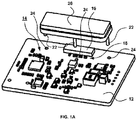
FIGS. 1A through 1E are schematic perspective views illustrating a method for manufacturing an electronic device in accordance with an embodiment of the present invention; -
FIG. 2 is a schematic flow diagram illustrating a method for optimising a matching circuitry of the electronic device in accordance with an embodiment of the present invention; -
FIG. 3 is a graph showing radio frequency (RF) performances of three (3) electronic devices manufactured in accordance with embodiments of the present invention as compared to three (3) electronic devices encapsulated without first attaching a cap over respective antennas and matching circuitry across the 2.4 GHz ISM band; -
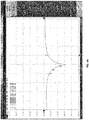
FIGS. 4A ,4B and4C are graphs showing return loss of three (3) electronic devices encapsulated without first attaching a cap over respective antennas and matching circuitry across the 2.4 GHz ISM band; and -
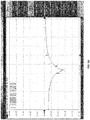
FIGS. 5A ,5B and5C are graphs showing return loss of three (3) electronic devices manufactured in accordance with embodiments of the present invention across the 2.4 GHz ISM band. - The detailed description set forth below in connection with the appended drawings is intended as a description of presently preferred embodiments of the invention, and is not intended to represent the only forms in which the present invention may be practiced. It is to be understood that the same or equivalent functions may be accomplished by different embodiments that are intended to be encompassed within the scope of the invention.
- A method for manufacturing an
electronic device 10 will now be described below with reference toFIGS. 1A through 1E . - Referring now to
FIG. 1A , asubstrate 12 having a plurality of radio-frequency components 14 provided thereon is provided as shown. The radio-frequency components include anantenna 16 and amatching circuitry 18. - In the embodiment shown, the
substrate 12 and the radio-frequency components 14 are provided in the form of a radio frequency (RF) radio module with associated circuitry on a printed circuit board (PCB). Theantenna 16 and thematching circuitry 18 are configured to transmit the RF signal. Thematching circuitry 18 is formed of a set of electronic components that are used to fine tune a frequency at which theantenna 16 outputs. - Referring now to
FIGS. 1A through 1C , a cap orcover 20 is attached to thesubstrate 12 over theantenna 16 and thematching circuitry 18. - This may involve aligning a plurality of
pins 22 of thecap 20 with corresponding ones of a plurality ofholes 24 in thesubstrate 12. In the present embodiment, thecap 20 is located in place using the locatingpins 22 at each end of thecap 20 which are received in the matchingholes 24 in thesubstrate 12. In an alternative embodiment, thepins 22 may be located at one or more corners of thecap 20. - The
cap 20 may then be heat staked to thesubstrate 12 by means of thepins 22. After heat staking, the heat stakedpins 22 form respective rivets that help hold thecap 20 in place during subsequent processing steps and prevent seepage of mold compound into an air space beneath thecap 20. In this manner, thecap 20 may be anchored to thesubstrate 12. - In the present embodiment, the
substrate 12 is designed such that there are no open via holes in the area covered by thecap 20. This is so that mold compound cannot enter into the space under thecap 20 through an open via hole. - In the same or a different embodiment, the
cap 20 may be bonded to the substrate 23 with anadhesive 26. Theadhesive 26 may be a room temperature vulcanizing silicone. Advantageously, theadhesive 26 helps to seal thecap 20 and prevent mold compound from intruding into antenna area under thecap 20. - The
cap 20 is positioned to cover theantenna 16 and thematching circuitry 18 and serves to protect theantenna 16 and thematching circuitry 18 from an external environment, providing a sealed environment for the electronics within to operate. A transceiver (not shown) may also be covered by thecap 20. Thepre-formed cap 20 may be machined from a polycarbonate material or may be made of another type of material that would allow RF to radiate through. In the present embodiment, thecap 20 is machined with thepins 22 on either side from polycarbonate to fit over theantenna 16 and thematching circuitry 18. - Referring now to
FIGS. 1D and 1E , a molding operation is performed to encapsulate thecap 20 and at least a portion of thesubstrate 12 with amold compound 28. This may be by placing thesubstrate 12 with theantenna 16 and thematching circuitry 18 sealed by thecap 20 in amold 30 and injecting themold compound 28 into themold 30 at an injection pressure of between about 1.02 kilograms per square centimetres (kg/cm2) and about 61.2 kg/cm2 and an injection temperature of between about 170 degrees Celsius (°C) and about 240 °C. - The
mold 30 in which thesubstrate 12 and the sealedcap 20 are enclosed may be designed for low pressure overmolding. - The
mold compound 28 protects the radio-frequency components 14 from the external environment and is of a type of material that would allow RF to radiate through. In one embodiment, themold compound 28 may be a hot melt polyamide material such as, for example, TECHNOMELT®, and may be injected into themold 30 at a temperature of about 180 degrees Celsius (°C) and an injection pressure of about 2.5 kg/cm2 for an injection period of about 8 seconds (s). Themold compound 28 may then be held in themold 30 for a holding time of about 15 s before being cooled for a cooling period of about 80 s. - By enclosing the radio-
frequency components 14 within a low pressure overmolded material, a sealed environment is provided for the electronics within to operate. - Further advantageously, by providing a sealed
cap 20 over theantenna 16 and thematching circuitry 18 before performing the molding operation, inconsistencies that may have arisen due to how molding material flows over theantenna 16 during the injection process and void formation within the overmold preventing theantenna 16 and thematching circuitry 18 from being evenly coated may be eliminated. - The
electronic device 10 that is produced from the manufacturing method described above may then be removed from themold 30 and is ready for testing. - To account for differences when the
antenna 16 is enclosed by themold compound 28 as opposed to air, thematching circuitry 18 may be optimised against a plurality of reference parameters from an unencapsulated antenna before the step of attaching thecap 20 to thesubstrate 12 in order to adjust a frequency of transmission back to a frequency of interest. The reference parameters may be obtained by measuring the antenna performance of a reference sample of an unencapsulated RF radio with matching circuitry and storing the RF performance parameters obtained as a reference. - Referring now to
FIG. 2 , amethod 50 for optimising thematching circuitry 16 of theelectronic device 10 will now be described. Themethod 50 begins atstep 52 by manufacturing a plurality of sample electronic devices. Several identical samples of the reference sample may be made and a first one of them may then be encapsulated using the manufacturing method described above with reference toFIGS. 1A through 1E , in particular, with the antenna and the matching circuitry covered by a cap before encapsulating the entire device. - At
step 54, an antenna performance of successive ones of the sample electronic devices is compared against the reference parameters from the unencapsulated antenna. The first encapsulated sample may be measured to obtain the RF antenna and matching circuitry performance parameters. These parameters are then compared with the reference parameters. - At
step 56, the successive ones of the sample electronic devices may be tuned to compensate for differences between the reference parameters from the unencapsulated antenna and the antenna performance of the successive ones of the sample electronic devices. Any shift in performance may be corrected by calculation and new matching circuitry values may be obtained by compensating for any shift in performance as measured in the encapsulated unit. - The optimisation steps are repeated with new matching circuitry values used in each iteration until the performance of the encapsulated unit is equivalent to the reference sample.
- The matching
circuitry 18 may then be tuned atstep 58 in accordance with a plurality of matching circuitry values determined when the antenna performance of one of the sample electronic devices matches the reference parameters from the unencapsulated antenna. In this manner, theelectronic devices 10 manufactured in accordance with the above described manufacturing method may be optimised for consistent performance despite being encapsulated. - Experiments were performed to study the RF performance and return loss of three (3)
electronic devices 10 formed in accordance with embodiments of the present invention and this was compared to that of three (3) electronic devices encapsulated using low pressure molding directly onto the electronic circuit without using a cap to cover the antenna and the matching circuitry as a control. The results of the experiments are shown inFIGS. 3 ,4A through 4C and5A through 5C . - As can be seen from
FIG. 3 , the antenna efficiency of the devices with caps is higher by between 5% and 20% compared to those without caps across the 2.4 GHz ISM band.FIGS. 4A through 4C 5A through 5C , also show that the three (3) devices with cap perform better in terms of return loss across the 2.4 GHz ISM band than those without caps. - As is evident from the foregoing discussion, the present invention provides a method for manufacturing an electronic device that provides protection for the RF antenna against external contamination from the environment and external environmental stresses during the manufacturing process. Advantageously, this helps ensure the stability of operation of the RF antenna of the electronic device that is formed within an intended RF band. Further advantageously, by optimising the matching circuitry of the electronic device against reference parameters from a reference sample before capping and encapsulation, consistency in RF performance may be achieved.
- While preferred embodiments of the invention have been illustrated and described, it will be clear that the invention is not limited to the described embodiments only. Numerous modifications, changes, variations, substitutions and equivalents will be apparent to those skilled in the art without departing from the scope of the invention as described in the claims. The manufacturing method of the present invention may be applied to electronic RF devices operating in any frequency such as, for example, the 2.4 GHz ISM band for Bluetooth beacons.
- Further, unless the context clearly requires otherwise, throughout the description and the claims, the words "comprise", "comprising" and the like are to be construed in an inclusive as opposed to an exclusive or exhaustive sense; that is to say, in the sense of "including, but not limited to".
Claims (11)
- A method for manufacturing an electronic device, comprising:providing a substrate having a plurality of radio-frequency components provided thereon, the radio-frequency components comprising an antenna and a matching circuitry;attaching a cap to the substrate over the antenna and the matching circuitry; andperforming a molding operation to encapsulate the cap and at least a portion of the substrate with a mold compound.
- The method of claim 1, further comprising optimising the matching circuitry against a plurality of reference parameters from an unencapsulated antenna before the step of attaching the cap to the substrate.
- The method of claim 2, wherein the step of optimising the matching circuitry comprises:manufacturing a plurality of sample electronic devices; andcomparing an antenna performance of successive ones of the sample electronic devices against the reference parameters from the unencapsulated antenna.
- The method of claim 3, wherein the step of optimising the matching circuitry further comprises:
tuning the successive ones of the sample electronic devices to compensate for differences between the reference parameters from the unencapsulated antenna and the antenna performance of the successive ones of the sample electronic devices. - The method of claim 4, wherein the step of optimising the matching circuitry further comprises:
tuning the matching circuitry in accordance with a plurality of matching circuitry values determined when the antenna performance of one of the sample electronic devices matches the reference parameters from the unencapsulated antenna. - The method of any one of the preceding claims, wherein the step of attaching the cap to the substrate comprises bonding the cap to the substrate with an adhesive.
- The method of claim 6, wherein the adhesive comprises a room temperature vulcanizing silicone.
- The method of any one of the preceding claims, wherein the step of attaching the cap to the substrate comprises aligning a plurality of pins of the cap with corresponding ones of a plurality of holes in the substrate.
- The method of claim 8, wherein the step of attaching the cap to the substrate further comprises heat staking the cap to the substrate by means of the pins.
- The method of any one of the preceding claims, further comprising machining the cap from a polycarbonate material.
- The method of any one of the preceding claims, wherein the step of performing the molding operation comprises:placing the substrate with the antenna and the matching circuitry sealed by the cap in a mold; andinjecting the mold compound into the mold at an injection pressure of between about 1.02 kilograms per square centimetres (kg/cm2) and about 61.2 kg/cm2.
Applications Claiming Priority (1)
| Application Number | Priority Date | Filing Date | Title |
|---|---|---|---|
| SG10201906867RA SG10201906867RA (en) | 2019-07-25 | 2019-07-25 | Method for manufacturing electronic device |
Publications (3)
| Publication Number | Publication Date |
|---|---|
| EP3771032A1 true EP3771032A1 (en) | 2021-01-27 |
| EP3771032B1 EP3771032B1 (en) | 2025-10-22 |
| EP3771032C0 EP3771032C0 (en) | 2025-10-22 |
Family
ID=71401685
Family Applications (1)
| Application Number | Title | Priority Date | Filing Date |
|---|---|---|---|
| EP20183031.2A Active EP3771032B1 (en) | 2019-07-25 | 2020-06-30 | Method for manufacturing electronic device |
Country Status (3)
| Country | Link |
|---|---|
| US (1) | US11464118B2 (en) |
| EP (1) | EP3771032B1 (en) |
| SG (1) | SG10201906867RA (en) |
Citations (3)
| Publication number | Priority date | Publication date | Assignee | Title |
|---|---|---|---|---|
| US20050078040A1 (en) * | 2003-09-29 | 2005-04-14 | Yokowo Co., Ltd. | Antenna structure |
| US20080309574A1 (en) * | 2007-06-12 | 2008-12-18 | Ethertronics Inc | System and method for preventing copying of electronic component designs |
| US20090295675A1 (en) * | 2008-05-27 | 2009-12-03 | Chia-Lun Tang | IC package antenna |
Family Cites Families (23)
| Publication number | Priority date | Publication date | Assignee | Title |
|---|---|---|---|---|
| DE4414005C2 (en) | 1993-04-22 | 2000-11-30 | Micron Technology Inc N D Ges | Process for encasing electronic components |
| JPH08276458A (en) | 1995-04-06 | 1996-10-22 | Dainippon Printing Co Ltd | Non-contact IC tag manufacturing method and non-contact IC tag |
| US6060342A (en) | 1998-04-06 | 2000-05-09 | P-Com, Incorporated | Circuit packaging for millimeter-wave components |
| DE19848712A1 (en) | 1998-10-22 | 2000-04-27 | Henkel Kgaa | Thermoplastics hot melt adhesive application for formation of smart card component layer or electronic transponder |
| JP3492533B2 (en) | 1998-12-16 | 2004-02-03 | Smk株式会社 | Helical antenna molding method |
| EP1052595B1 (en) | 1999-05-14 | 2001-09-19 | Sokymat Sa | Transponder and injection-moulded object and method for manufacturing the same |
| US6441741B1 (en) | 1999-05-17 | 2002-08-27 | Avid Identification Systems, Inc. | Overmolded transponder |
| ATE240195T1 (en) | 2000-02-11 | 2003-05-15 | Robert Virant | MOLDED, ELECTRICAL AND/OR ELECTRONIC COMPONENT AND METHOD FOR PRODUCTION |
| DE10162450B4 (en) | 2001-12-19 | 2008-06-05 | Giesecke & Devrient Gmbh | Portable data carrier and method and device for manufacturing |
| US6977187B2 (en) * | 2002-06-19 | 2005-12-20 | Foster-Miller, Inc. | Chip package sealing method |
| JP2008537215A (en) | 2005-03-23 | 2008-09-11 | カードエックスエックス インコーポレイテッド | A method of manufacturing a modern smart card with integrated electronics using an isotropic thermoset adhesive material having a high quality outer surface. |
| US20070171076A1 (en) | 2005-08-29 | 2007-07-26 | Visible Assets, Inc. | Low-frequency radio tag encapsulating system |
| US20080282540A1 (en) | 2007-05-14 | 2008-11-20 | Innovatier, Inc. | Method for making advanced smart cards with integrated electronics using isotropic thermoset adhesive materials with high quality exterior surfaces |
| US20100033400A1 (en) | 2008-08-05 | 2010-02-11 | Daniel Chang | Spray non-contact cutting type antenna and its fabrication method |
| US8325047B2 (en) | 2009-04-08 | 2012-12-04 | Sabic Innovative Plastics Ip B.V. | Encapsulated RFID tags and methods of making same |
| DE102011052501A1 (en) | 2011-08-08 | 2013-02-14 | Aesculap Ag | RFID tag |
| FR2990314B1 (en) | 2012-05-03 | 2014-06-06 | Commissariat Energie Atomique | MICROELECTRONIC DEVICE FOR WIRELESS TRANSMISSION |
| JP6373721B2 (en) * | 2014-01-15 | 2018-08-15 | 株式会社日立製作所 | Communication apparatus and manufacturing method thereof |
| JP6314705B2 (en) | 2014-07-04 | 2018-04-25 | 富士通株式会社 | High frequency module and manufacturing method thereof |
| DE102014223653B4 (en) | 2014-11-20 | 2023-08-03 | Zf Friedrichshafen Ag | Electrical circuit and method of making an electrical circuit for a vehicle |
| US10037951B2 (en) * | 2016-11-29 | 2018-07-31 | Cyntec Co., Ltd. | Semiconductor package with antenna |
| TWI609329B (en) | 2016-12-19 | 2017-12-21 | 韋僑科技股份有限公司 | Rfid device and method for making the same |
| US10263332B2 (en) * | 2017-09-18 | 2019-04-16 | Apple Inc. | Antenna arrays with etched substrates |
-
2019
- 2019-07-25 SG SG10201906867RA patent/SG10201906867RA/en unknown
-
2020
- 2020-06-30 EP EP20183031.2A patent/EP3771032B1/en active Active
- 2020-07-20 US US16/933,418 patent/US11464118B2/en active Active
Patent Citations (3)
| Publication number | Priority date | Publication date | Assignee | Title |
|---|---|---|---|---|
| US20050078040A1 (en) * | 2003-09-29 | 2005-04-14 | Yokowo Co., Ltd. | Antenna structure |
| US20080309574A1 (en) * | 2007-06-12 | 2008-12-18 | Ethertronics Inc | System and method for preventing copying of electronic component designs |
| US20090295675A1 (en) * | 2008-05-27 | 2009-12-03 | Chia-Lun Tang | IC package antenna |
Non-Patent Citations (1)
| Title |
|---|
| FRANK ONGKIEHONG AND STEVEN DUFRESNE: "Circuits Assembly Online Magazine - Low Pressure Molding: A Primer", 28 December 2005 (2005-12-28), XP055753845, Retrieved from the Internet <URL:https://www.circuitsassembly.com/ca/news/370-magazine-articles/2006-articles/11711-low-pressure-molding-a-primer.html> [retrieved on 20201125] * |
Also Published As
| Publication number | Publication date |
|---|---|
| EP3771032B1 (en) | 2025-10-22 |
| US20210029833A1 (en) | 2021-01-28 |
| US11464118B2 (en) | 2022-10-04 |
| EP3771032C0 (en) | 2025-10-22 |
| SG10201906867RA (en) | 2021-02-25 |
Similar Documents
| Publication | Publication Date | Title |
|---|---|---|
| US20180219281A1 (en) | Antenna device and method for manufacturing antenna device | |
| US10581157B2 (en) | Antenna-integrated wireless module and method for manufacturing antenna-integrated wireless module | |
| US10888040B2 (en) | Double-sided module with electromagnetic shielding | |
| CN110024223B (en) | Conduction type OTA test fixture | |
| US10978778B2 (en) | Wafer level package with integrated antennas and means for shielding | |
| US9570406B2 (en) | Wafer level fan-out with electromagnetic shielding | |
| KR20230088314A (en) | Packaged electronic device having integrated antenna and locking structure | |
| US7659604B2 (en) | Module component and method for manufacturing the same | |
| US7057564B2 (en) | Multilayer cavity slot antenna | |
| TWI652789B (en) | Components and methods related to packaging of radio frequency components on ceramic substrates | |
| US20190221531A1 (en) | On-Chip Antennas for Semiconductor Devices and Related Manufacturing Methods | |
| JP2001148603A (en) | Antenna package for radio communication equipment | |
| US20210351503A1 (en) | Antenna module and communication device | |
| US9230944B1 (en) | Techniques and configurations associated with a capductor assembly | |
| US7971350B2 (en) | Method of providing a RF shield of an electronic device | |
| US11131770B2 (en) | Vehicle radar | |
| US20180191051A1 (en) | Wafer level package with at least one integrated antenna element | |
| US20200303318A1 (en) | Shielded electronic modules and methods of forming the same utilizing plating and double-cut singulation | |
| US20120002381A1 (en) | Method for manufacturing a liquid-tight electronic device, and liquid-tight electronic device | |
| US20250183516A1 (en) | Microelectronic Device Package Including Antenna Horn and Semiconductor Device | |
| US11464118B2 (en) | Method for manufacturing electronic device | |
| US20220051908A1 (en) | Fan-out Packaging Method and Fan-out Packaging Plate | |
| US20230268304A1 (en) | Semiconductor device with open cavity and method therefor | |
| KR102230907B1 (en) | Plastic Patch Antenna and Method for Producing the Same | |
| US20210125021A1 (en) | Radio-frequency device with radio-frequency signal carrying element and associated production method |
Legal Events
| Date | Code | Title | Description |
|---|---|---|---|
| PUAI | Public reference made under article 153(3) epc to a published international application that has entered the european phase |
Free format text: ORIGINAL CODE: 0009012 |
|
| STAA | Information on the status of an ep patent application or granted ep patent |
Free format text: STATUS: THE APPLICATION HAS BEEN PUBLISHED |
|
| AK | Designated contracting states |
Kind code of ref document: A1 Designated state(s): AL AT BE BG CH CY CZ DE DK EE ES FI FR GB GR HR HU IE IS IT LI LT LU LV MC MK MT NL NO PL PT RO RS SE SI SK SM TR |
|
| AX | Request for extension of the european patent |
Extension state: BA ME |
|
| STAA | Information on the status of an ep patent application or granted ep patent |
Free format text: STATUS: REQUEST FOR EXAMINATION WAS MADE |
|
| 17P | Request for examination filed |
Effective date: 20210706 |
|
| RBV | Designated contracting states (corrected) |
Designated state(s): AL AT BE BG CH CY CZ DE DK EE ES FI FR GB GR HR HU IE IS IT LI LT LU LV MC MK MT NL NO PL PT RO RS SE SI SK SM TR |
|
| STAA | Information on the status of an ep patent application or granted ep patent |
Free format text: STATUS: EXAMINATION IS IN PROGRESS |
|
| 17Q | First examination report despatched |
Effective date: 20221013 |
|
| REG | Reference to a national code |
Ref country code: DE Ref legal event code: R079 Free format text: PREVIOUS MAIN CLASS: H01Q0001400000 Ipc: H01Q0001420000 Ref country code: DE Ref legal event code: R079 Ref document number: 602020060744 Country of ref document: DE Free format text: PREVIOUS MAIN CLASS: H01Q0001400000 Ipc: H01Q0001420000 |
|
| GRAP | Despatch of communication of intention to grant a patent |
Free format text: ORIGINAL CODE: EPIDOSNIGR1 |
|
| STAA | Information on the status of an ep patent application or granted ep patent |
Free format text: STATUS: GRANT OF PATENT IS INTENDED |
|
| RIC1 | Information provided on ipc code assigned before grant |
Ipc: H05K 1/02 20060101ALN20250417BHEP Ipc: H01Q 1/40 20060101ALI20250417BHEP Ipc: H05K 3/28 20060101ALI20250417BHEP Ipc: H01Q 1/42 20060101AFI20250417BHEP |
|
| RIC1 | Information provided on ipc code assigned before grant |
Ipc: H05K 1/02 20060101ALN20250428BHEP Ipc: H01Q 1/40 20060101ALI20250428BHEP Ipc: H05K 3/28 20060101ALI20250428BHEP Ipc: H01Q 1/42 20060101AFI20250428BHEP |
|
| INTG | Intention to grant announced |
Effective date: 20250514 |
|
| GRAS | Grant fee paid |
Free format text: ORIGINAL CODE: EPIDOSNIGR3 |
|
| GRAA | (expected) grant |
Free format text: ORIGINAL CODE: 0009210 |
|
| STAA | Information on the status of an ep patent application or granted ep patent |
Free format text: STATUS: THE PATENT HAS BEEN GRANTED |
|
| AK | Designated contracting states |
Kind code of ref document: B1 Designated state(s): AL AT BE BG CH CY CZ DE DK EE ES FI FR GB GR HR HU IE IS IT LI LT LU LV MC MK MT NL NO PL PT RO RS SE SI SK SM TR |
|
| REG | Reference to a national code |
Ref country code: CH Ref legal event code: F10 Free format text: ST27 STATUS EVENT CODE: U-0-0-F10-F00 (AS PROVIDED BY THE NATIONAL OFFICE) Effective date: 20251022 Ref country code: GB Ref legal event code: FG4D |
|
| REG | Reference to a national code |
Ref country code: DE Ref legal event code: R096 Ref document number: 602020060744 Country of ref document: DE |
|
| REG | Reference to a national code |
Ref country code: IE Ref legal event code: FG4D |
|
| U01 | Request for unitary effect filed |
Effective date: 20251121 |
|
| U07 | Unitary effect registered |
Designated state(s): AT BE BG DE DK EE FI FR IT LT LU LV MT NL PT RO SE SI Effective date: 20251128 |
|
| PG25 | Lapsed in a contracting state [announced via postgrant information from national office to epo] |
Ref country code: ES Free format text: LAPSE BECAUSE OF FAILURE TO SUBMIT A TRANSLATION OF THE DESCRIPTION OR TO PAY THE FEE WITHIN THE PRESCRIBED TIME-LIMIT Effective date: 20251022 |
|
| PG25 | Lapsed in a contracting state [announced via postgrant information from national office to epo] |
Ref country code: NO Free format text: LAPSE BECAUSE OF FAILURE TO SUBMIT A TRANSLATION OF THE DESCRIPTION OR TO PAY THE FEE WITHIN THE PRESCRIBED TIME-LIMIT Effective date: 20260122 |
|
| PG25 | Lapsed in a contracting state [announced via postgrant information from national office to epo] |
Ref country code: HR Free format text: LAPSE BECAUSE OF FAILURE TO SUBMIT A TRANSLATION OF THE DESCRIPTION OR TO PAY THE FEE WITHIN THE PRESCRIBED TIME-LIMIT Effective date: 20251022 |
|
| PG25 | Lapsed in a contracting state [announced via postgrant information from national office to epo] |
Ref country code: RS Free format text: LAPSE BECAUSE OF FAILURE TO SUBMIT A TRANSLATION OF THE DESCRIPTION OR TO PAY THE FEE WITHIN THE PRESCRIBED TIME-LIMIT Effective date: 20260122 |
|
| PG25 | Lapsed in a contracting state [announced via postgrant information from national office to epo] |
Ref country code: IS Free format text: LAPSE BECAUSE OF FAILURE TO SUBMIT A TRANSLATION OF THE DESCRIPTION OR TO PAY THE FEE WITHIN THE PRESCRIBED TIME-LIMIT Effective date: 20260222 |
|
| PG25 | Lapsed in a contracting state [announced via postgrant information from national office to epo] |
Ref country code: PL Free format text: LAPSE BECAUSE OF FAILURE TO SUBMIT A TRANSLATION OF THE DESCRIPTION OR TO PAY THE FEE WITHIN THE PRESCRIBED TIME-LIMIT Effective date: 20251022 |
|
| U1N | Appointed representative for the unitary patent procedure changed after the registration of the unitary effect |
Representative=s name: MARKS & CLERK LLP; GB |